WO2025028014A1 - 試験装置 - Google Patents
試験装置 Download PDFInfo
- Publication number
- WO2025028014A1 WO2025028014A1 PCT/JP2024/020532 JP2024020532W WO2025028014A1 WO 2025028014 A1 WO2025028014 A1 WO 2025028014A1 JP 2024020532 W JP2024020532 W JP 2024020532W WO 2025028014 A1 WO2025028014 A1 WO 2025028014A1
- Authority
- WO
- WIPO (PCT)
- Prior art keywords
- substrate
- test
- light
- test signal
- signal
- Prior art date
- Legal status (The legal status is an assumption and is not a legal conclusion. Google has not performed a legal analysis and makes no representation as to the accuracy of the status listed.)
- Pending
Links
Images




Classifications
-
- G—PHYSICS
- G01—MEASURING; TESTING
- G01R—MEASURING ELECTRIC VARIABLES; MEASURING MAGNETIC VARIABLES
- G01R15/00—Details of measuring arrangements of the types provided for in groups G01R17/00 - G01R29/00, G01R33/00 - G01R33/26 or G01R35/00
- G01R15/14—Adaptations providing voltage or current isolation, e.g. for high-voltage or high-current networks
- G01R15/24—Adaptations providing voltage or current isolation, e.g. for high-voltage or high-current networks using light-modulating devices
-
- G—PHYSICS
- G01—MEASURING; TESTING
- G01R—MEASURING ELECTRIC VARIABLES; MEASURING MAGNETIC VARIABLES
- G01R19/00—Arrangements for measuring currents or voltages or for indicating presence or sign thereof
-
- G—PHYSICS
- G01—MEASURING; TESTING
- G01R—MEASURING ELECTRIC VARIABLES; MEASURING MAGNETIC VARIABLES
- G01R29/00—Arrangements for measuring or indicating electric quantities not covered by groups G01R19/00 - G01R27/00
- G01R29/08—Measuring electromagnetic field characteristics
-
- G—PHYSICS
- G01—MEASURING; TESTING
- G01R—MEASURING ELECTRIC VARIABLES; MEASURING MAGNETIC VARIABLES
- G01R31/00—Arrangements for testing electric properties; Arrangements for locating electric faults; Arrangements for electrical testing characterised by what is being tested not provided for elsewhere
- G01R31/28—Testing of electronic circuits, e.g. by signal tracer
-
- G—PHYSICS
- G01—MEASURING; TESTING
- G01R—MEASURING ELECTRIC VARIABLES; MEASURING MAGNETIC VARIABLES
- G01R31/00—Arrangements for testing electric properties; Arrangements for locating electric faults; Arrangements for electrical testing characterised by what is being tested not provided for elsewhere
- G01R31/28—Testing of electronic circuits, e.g. by signal tracer
- G01R31/302—Contactless testing
- G01R31/308—Contactless testing using non-ionising electromagnetic radiation, e.g. optical radiation
- G01R31/309—Contactless testing using non-ionising electromagnetic radiation, e.g. optical radiation of printed or hybrid circuits or circuit substrates
-
- H—ELECTRICITY
- H05—ELECTRIC TECHNIQUES NOT OTHERWISE PROVIDED FOR
- H05K—PRINTED CIRCUITS; CASINGS OR CONSTRUCTIONAL DETAILS OF ELECTRIC APPARATUS; MANUFACTURE OF ASSEMBLAGES OF ELECTRICAL COMPONENTS
- H05K3/00—Apparatus or processes for manufacturing printed circuits
Definitions
- This disclosure relates to a testing device.
- An electromagnetic field imaging device that uses the Pockels effect is known as a device for non-contact detection of the electromagnetic field distribution of a substrate operating at a certain operating frequency.
- This electromagnetic field imaging device places an electro-optic element, whose birefringence changes with an electric field, near the substrate to be observed, applies a signal at the operating frequency of the substrate to the substrate, and irradiates the electro-optic element with laser light modulated at a modulation frequency set according to the operating frequency of the substrate.
- the imaging device captures, as an image, detection light that contains a difference frequency component between the modulation frequency and the operating frequency generated in the electro-optic element.
- a configuration for modulating the laser light such as a Mach-Zehnder modulator (MZM) or an electro-absorption (EA) modulator, is required.
- MZM Mach-Zehnder modulator
- EA electro-absorption
- This configuration for modulating the laser light is relatively expensive. Furthermore, because the power of the laser light is reduced by modulation, the S/N ratio of the image obtained by the imaging device also tends to be low.
- This disclosure provides a substrate testing device with a simple configuration and good S/N ratio.
- test device includes an electro-optical sensor, a test signal application unit, a light source, and a camera.
- the electro-optical sensor is placed near the substrate to be tested, and changes the birefringence characteristics when it receives an electric field from the substrate.
- the test signal application unit applies a modulated test signal to the substrate.
- the light source irradiates illumination light onto the electro-optical sensor.
- the camera captures an image of the return light of the illumination light emitted from the electro-optical sensor in response to the illumination light from the light source when the test signal is applied to the substrate.
- This disclosure provides a substrate testing device with a simple configuration and good S/N ratio.
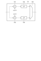
- FIG. 1 is a diagram showing an example of a configuration of a test apparatus according to an embodiment.
- FIG. 2 is a diagram illustrating an example of a configuration of the signal processing unit.
- FIG. 3 is a diagram illustrating an example of a configuration of a computer.
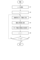
- FIG. 4 is a flow chart showing an example of a testing method using the testing device.
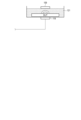
- FIG. 5 is a diagram showing a test in a state where the substrate is immersed in water.
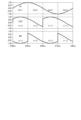
- FIG. 6 is a diagram conceptually showing quadrature demodulation of pixel signals of four frames when the cosine component pixel signals and the sine component pixel signals are out of phase with respect to the phase of the test signal.
- FIG. 1 is a diagram showing an example of a configuration of a test apparatus according to an embodiment.
- FIG. 2 is a diagram illustrating an example of a configuration of the signal processing unit.
- FIG. 3 is a diagram illustrating an example of a configuration of a computer.
- FIG. 4 is a flow chart
- FIG. 7 is a diagram conceptually showing quadrature demodulation of pixel signals of two frames when the phase of the test signal and the phase of the cosine component pixel signal match.
- FIG. 8 is a diagram showing an example of a configuration of a test apparatus according to the fourth modification.
- FIG. 9 is a diagram showing another example of the configuration of the signal processing unit according to the fourth modification.
- FIG. 1 is a diagram showing the configuration of an example of a test device according to the embodiments.
- the test device according to the embodiments is used to test a board that does not require the application of a signal of a specific operating frequency.
- a test of a board that does not require the application of a signal of a specific operating frequency is, for example, a continuity test of an interposer.
- the test device according to the embodiments can be used to test various boards other than interposers that do not require the application of a signal of a specific operating frequency.
- the test device 1 includes a laser device 101, a collimator lens 102, a quarter-wave plate 103, a half-wave plate 104, a polarizing beam splitter (PBS) 105, a quarter-wave plate 106, a half-wave plate 107, a mirror 108, an electro-optical (EO) sensor 109, an oscillator 110, a frequency divider/phase shifter 111, an amplitude modulator 112, a demultiplexer 113, an imaging lens 114, a camera 115, a signal processing unit 116, a computer 117, and probe electrodes 118, 119, and 120.
- the number of probe electrodes is described as three.
- the number of probe electrodes is not limited to three, and may be one or two, or may be four or more.
- the number of probe electrodes may be set appropriately according to, for example, the size of the substrate D and/or the number of connection pads.
- the laser device 101 is a light source that generates laser light as illumination light to be irradiated to the EO sensor 109.
- the laser device 101 irradiates the generated laser light to an object through, for example, an optical fiber.
- the laser light irradiated to the EO sensor 109 is, for example, a visible light laser.
- Collimator lens 102, 1/4 wavelength plate 103, 1/2 wavelength plate 104, PBS 105, 1/4 wavelength plate 106, 1/2 wavelength plate 107, and mirror 108 are disposed on the output optical path of laser device 101.
- Collimator lens 102, 1/4 wavelength plate 103, 1/2 wavelength plate 104, PBS 105, 1/4 wavelength plate 106, 1/2 wavelength plate 107, and mirror 108 can operate as a wavefront matching optical system for matching the wavefront of the output light of laser device 101 to the light irradiation surface of EO sensor 109.
- PBS 105, 1/4 wavelength plate 106, 1/2 wavelength plate 107, and mirror 108 can also operate as a detection optical system for converting the modulation of the polarization state output from EO sensor 109 into intensity modulation.
- Collimator lens 102 outputs the laser light incident from laser device 101 as parallel light.
- the laser light emitted from collimator lens 102 is circularly polarized by quarter-wave plate 103 and half-wave plate 104. This circularly polarized light travels straight through PBS 105, passes through quarter-wave plate 106 and half-wave plate 107, and then has its optical axis bent by mirror 108. The light with its optical axis bent is incident perpendicularly on EO sensor 109.
- the mirror 108 also reflects the light incident from the EO sensor 109 toward the half-wave plate 107.
- the EO sensor 109 is an electro-optical sensor that changes birefringence when an electric field is applied.
- the EO sensor 109 is made of an isotropic crystal plate such as ZnTe or LiNO3 .
- the EO sensor 109 is disposed near a device under test (DUT) D so that the EO sensor 109 can receive an electric field generated in the DUT D.
- DUT device under test
- the EO sensor 109 polarizes the incident light with a birefringence according to the strength of the electric field received from the DUT D, and emits the polarized light in the direction of the mirror 108.
- Oscillator 110 is an oscillator that generates a carrier wave.
- the carrier wave is, for example, a sine wave with a frequency fc.
- the frequency fc is a high frequency, for example, 10 GHz.
- the frequency divider/phase shifter 111 generates an amplitude modulated wave by dividing and phase shifting the carrier wave.
- the amplitude modulated wave is, for example, a sine wave with a modulation frequency fam.
- the modulation frequency fam is set to a frequency lower than the frame rate of the camera 115.
- the modulation frequency fam is set to a frequency equivalent to 1/4 of the frame rate of the camera 115.
- the amplitude modulator 112 which serves as a test signal application unit, generates a test signal by amplitude modulating a carrier wave with an amplitude modulated wave.
- the amplitude modulator 112 then applies the test signal to one of the probe electrodes 118, 119, or 120 via the demultiplexer 113.
- Figure 1 shows an example in which the amplitude modulator 112 applies the test signal to the probe electrode 119.
- demultiplexer 113 Based on instructions from computer 117, demultiplexer 113 selects the probe electrodes 118, 119, and 120 to which the test signal from amplitude modulator 112 is to be applied, and outputs the test signal to the selected probe electrode.
- the probe electrodes 118, 119, 120 are arranged on the surface of the substrate D opposite the surface facing the EO sensor 109, with a gap between them and the substrate D.
- the probe electrodes 118, 119, 120 are electrostatically coupled to the substrate D, and apply the test signal output from the amplitude modulator 112 to the substrate D in a non-contact manner.
- the substrate D is a substrate to which it is not necessary to apply a signal of a specific operating frequency, such as an interposer.
- the probe electrodes 118, 119, 120 are arranged near the respective connection pads of the interposer.
- the imaging lens 114 is disposed on the reflected light path of the PBS 105, and images the light incident from the PBS 105 onto the pixels of the camera 115.
- Camera 115 has an image sensor consisting of many pixels, and captures the light focused through imaging lens 114 to obtain a digital pixel signal.
- the image sensor is, for example, a CMOS image sensor. As will be explained later, camera 115 captures one frame at a frame rate equivalent to 4 fam input from amplitude modulator 112.
- the signal processing unit 116 is, for example, a digital signal processing unit (DSP), and performs signal processing on the pixel signals obtained by the camera 115.
- the signal processing includes processing for quadrature demodulation.
- the example of the signal processing unit 116 has a cosine component integrator 1161, a low pass filter (LPF) 1162, a sine component integrator 1163, a low pass filter (LPF) 1164, and a multiplexer 1165.
- the signal processing unit 116 may be configured integrally with the computer 117.
- the cosine component integrator 1161 multiplies the input signal by the cosine component cos2 ⁇ ft.
- f is a frequency and is equal to the modulation frequency fam.
- t is the time elapsed since the start of imaging by the camera 115.
- the cosine component integrator 1161 may multiply by a pseudo-cosine component.
- the pseudo-cosine component is a square wave approximating the cosine wave cos2 ⁇ ft with an amplitude of ⁇ 1.
- the cosine component integrator 1161 multiplies the input signal of the first frame by +1, the input signal of the second frame by +1, the input signal of the third frame by -1, and the input signal of the fourth frame by -1.
- an operation equivalent to that of the cosine component integrator 1161 may be performed by digital calculation.
- LPF 1162 removes harmonic components generated by the product of the input signal from camera 115 and the cosine component.
- FIR Finite Impulse Response
- IIR Infinite Impulse Response
- the sine component integrator 1163 multiplies the input signal by the sine component sin2 ⁇ ft.
- f is a frequency and is equal to the modulation frequency fam.
- t is the time elapsed since the start of imaging by the camera 115.
- the sine component integrator 1163 may multiply by a pseudo sine component.
- the pseudo sine component is an approximation of the sine wave sin2 ⁇ ft by a rectangular wave with an amplitude of ⁇ 1.
- the sine component integrator 1163 multiplies the input signal of the first frame by -1, the input signal of the second frame by +1, the input signal of the third frame by +1, and the input signal of the fourth frame by -1.
- an operation equivalent to that of the sine component integrator 1163 may be performed by digital calculation.
- LPF 1164 removes harmonic components that arise from the product of the input signal from camera 115 and the sine component.
- an FIR filter, an IIR filter, or the like an operation equivalent to that of LPF 1164 may be performed by digital calculation.
- the multiplexer 1165 combines the input signals from the LPFs 1162 and 1164 and outputs them to the computer 117.
- Computer 117 is a computer that controls the operation of test device 1.
- Computer 117 calculates the amplitude and phase of the return light that represents the change in birefringence of EO sensor 109 from the output of signal processing unit 116, for example.
- Computer 117 also displays the calculated amplitude and phase of the return light as an image.
- computer 117 can also control the operation of laser device 101 and oscillator 110.
- FIG. 3 is a diagram showing an example of the configuration of computer 117.
- Computer 117 is, for example, a personal computer, and has a processor 1171, memory 1172, storage 1173, input interface 1174, and output interface 1175 as hardware.
- Processor 1171, memory 1172, storage 1173, input interface 1174, and output interface 1175 are connected to a bus.
- Processor 1171 is a processor that controls the overall operation of computer 117. Processor 1171 can perform various processes by executing programs stored in storage 1173, for example. Processor 1171 is, for example, a CPU. Processor 1171 may be an MPU, a GPU, or the like. Also, an ASIC, an FPGA, or the like may be used instead of processor 1171. Processor 1171 may be a single CPU, or the like, or multiple CPUs, or the like.
- Memory 1172 includes ROM and RAM.
- ROM is a non-volatile memory. ROM stores the startup program of computer 117 and the like.
- RAM is a volatile memory. RAM is used, for example, as a working memory during processing in processor 1171.
- Storage 1173 is, for example, a storage such as a hard disk drive or a solid state drive. Storage 1173 stores various programs executed by processor 1171, such as test program 1173a. In addition, storage 1173 may store calculated amplitude and phase values of the return light and/or image data representing the same.
- the input interface 1174 is an input device such as a touch panel, keyboard, or mouse. When the input interface 1174 is operated, a signal corresponding to the operation is input to the processor 1171 via the bus. The processor 1171 performs various processes according to this signal.
- the input interface 1174 may be used by an operator operating the test device 1 to make various settings related to the test device 1.
- the various settings include, for example, settings of the carrier frequency fc and the modulation frequency fam.
- the output interface 1175 includes a display device such as a liquid crystal display or an organic electroluminescence display.
- the output interface 1175 may be used to display the calculated amplitude and phase values of the returned light and/or an image representing them.
- the output interface 1175 may also include an output device for various information such as a printer instead of or in addition to the display device.
- the display device of the output interface 1175 does not necessarily need to be provided in the computer 117, and may be an external display device capable of communicating with the computer 117.
- Figure 4 is a flowchart showing an example of a test method using the test device 1.
- the following test method will be described using an interposer continuity test as an example.
- step S1 the computer 117 irradiates the substrate D with laser light.
- step S2 the computer 117 assigns 1 to the probe electrode number n.
- step S3 the computer 117 sends a control signal to the demultiplexer 113 to select the probe electrode n and apply a test signal to the probe electrode n.
- step S4 the computer 117 starts imaging with the camera 115.
- the pixel signal of each pixel of the camera 115 is subjected to processing for quadrature demodulation in the signal processing unit 116.
- the processed pixel signal data is then stored in, for example, the memory 1172 of the computer 117.
- the processing of steps S3 and S4 may be performed simultaneously.
- step S5 the computer 117 calculates the amplitude and phase of the return light for the image corresponding to the probe electrode number n.
- step S1-S5 The processing of steps S1-S5 will be described in detail below.
- computer 117 controls oscillator 110 to start outputting the carrier wave.
- Amplitude modulator 112 generates a test signal by amplitude modulating the carrier wave with the amplitude modulation wave generated by frequency divider/phase shifter 111.
- the test signal generated by amplitude modulator 112 is applied to one connection pad provided on the back surface of the interposer in a non-contact manner via demultiplexer 113 and probe electrode with probe electrode number n, probe electrode 119 in FIG. 1.
- the laser light emitted from the laser device 101 is collimated by the collimator lens 102.
- the light that passes through the collimator lens 102 passes through the quarter-wave plate 103 and the half-wave plate 104 and becomes circularly polarized light.
- This circularly polarized light is separated by entering the PBS 105.
- the polarized light component that passes through the PBS 105 is polarized by the quarter-wave plate 106 and the half-wave plate 107, and is then reflected by the mirror 108 and enters the EO sensor 109.
- a test signal with a frequency of fc ⁇ fam is applied to board D.
- an electric field whose intensity varies with frequency fc ⁇ fam is generated on the surface of board D depending on the state of continuity of board D.
- an electric field whose intensity varies with frequency fc ⁇ fam is generated on the surface pad connected to the pad on the back side of the interposer to which an electric field is applied by the probe electrode, and if there is no continuity, no electric field is generated on the surface pad.
- an electric field is observed on a surface pad that is not actually connected to a pad on the back side, it is clear that the wiring inside the interposer is short-circuited.
- the EO sensor 109 is disposed near the substrate D so that it receives an electric field from the substrate D and changes its birefringence at a frequency of fc ⁇ fam. Therefore, when the reflected light from the mirror 108 enters the EO sensor 109, the reflected light undergoes local polarization state modulation according to the birefringence characteristics of the EO sensor 109. Therefore, the return light from the EO sensor 109 contains light components with frequencies of fc ⁇ fam in addition to the frequency components of the original laser light.
- the returning light from the EO sensor 109 is reflected by the mirror 108.
- the polarization state modulation of the returning light is then converted to intensity modulation by passing through the half-wave plate 107, the quarter-wave plate 106, and the PBS 105.
- This returning light is then imaged on the pixels of the camera 115 via the imaging lens 114. Since the camera 115 captures images at a frame rate equivalent to 4 fam, the light with the frequency fam component is captured by the camera 115.
- the light with the frequency fam component is light that reflects the birefringence characteristics of the EO sensor 109, i.e., the state of the electric field of the substrate D.
- the signal processing unit 116 After the camera 115 has completed capturing one frame, the signal processing unit 116 performs the following processes for orthogonal demodulation: multiplying the pixel signal of each pixel of the camera 115 by a cosine component or a pseudo cosine component to remove high frequency components, and multiplying the pixel signal by a sine component or a pseudo sine component to remove high frequency components.
- the signal processing unit 116 associates the cosine component pixel signals and sine component pixel signals obtained by these processes with the pixel positions and transfers them to the computer 117.
- the computer 117 stores the data transferred from the signal processing unit 116, for example, in the memory 1172.
- the camera 115 captures the return light at a frame rate equivalent to four times the modulation frequency fam. That is, four frames are required to capture one cycle of the return light.
- the computer 117 calculates the amplitude and phase of the return light for the probe electrode number n from the cosine component pixel signal and the sine component pixel signal obtained by the signal processing unit 116. Specifically, the computer 117 calculates the integral value of each of one cycle of the cosine component pixel signal and the sine component pixel signal.
- the computer 117 calculates the amplitude A of the return light from the sum of the squares of the integral value of one cycle of the cosine component pixel signal and the integral value of one cycle of the sine component pixel signal based on the following formula (1).
- the computer 117 calculates the phase P of the return light from the ratio of the integral value of one cycle of the cosine component pixel signal and the integral value of one cycle of the sine component pixel signal based on the following formula (2).
- M in formula (1) is the amplitude of the integrated cosine component pixel signal and the sine component pixel signal.
- step S6 the computer 117 adds +1 to the probe electrode number n.
- step S7 the computer 117 determines whether the probe electrode number n is nend. nend is a number representing the last probe electrode. In step S7, if the probe electrode number n is not the last probe electrode number nend, the process returns to step S3. In this case, the operations from steps S3 to S5 are performed on the next probe electrode. In step S7, if the probe electrode number n is the last probe electrode number nend, the process ends.
- the computer 117 may display the amplitude and phase information as a two-dimensional image on the display device by assigning pixel values according to the magnitude of the amplitude and phase to each of the amplitude and phase calculated for each pixel of the camera 115.
- the image representing the amplitude and phase information is an image representing the state of the electric field on the surface of the interposer as the substrate D.
- the conductive or non-conductive state of the interposer can be grasped from the distribution of the amplitude and phase.
- the computer 117 knows in advance from the interposer design data which positions of pads on the surface are expected to be detected when a test signal is applied to each probe electrode.
- the laser light is not modulated, and a modulated test signal is applied to the board.
- the modulation frequency of the test signal is not required. Therefore, the test device of the embodiment has a simple configuration that does not require an MZM or the like for modulating the laser light.
- modulation of the laser light is not required, there is no loss of power of the laser light due to modulation of the laser light. As a result, the S/N ratio of the image obtained by the camera can be improved.
- the test signal is applied without contact due to electrostatic coupling between the board and the probe electrode. Therefore, testing can be performed even in situations where it is difficult to make contact with the probe electrode due to reasons such as the small connection pads on the board. Furthermore, by using a modulated test signal, the test signal can be applied with low loss by increasing the carrier frequency even if the coupling capacitance between the board and the probe electrode is small.
- test signal is applied in a non-contact manner using capacitive coupling, but the test signal does not necessarily have to be applied in a non-contact manner.
- test 2 When the size of the substrate is large relative to the size of the EO sensor or when the angle of view of the camera is narrow, the test for the entire area of the substrate cannot be completed in one test. In this case, the test may be performed multiple times by changing the EO sensor and the irradiation position of the laser light.
- the embodiments do not specifically mention the medium between the probe electrode and the substrate and between the substrate and the EO sensor. If the test were to be performed in air, air would be present between the probe electrode and the substrate and between the substrate and the EO sensor. Since the dielectric constant of air is small, if air is present between the probe electrode and the substrate and between the substrate and the EO sensor, the loss at each location would be large.
- the coupling loss is inversely proportional to the coupling capacitance.
- the space between the probe electrode and the substrate and the space between the substrate and the EO sensor can be filled with a medium having a higher dielectric constant than air.
- the space can be filled with a medium having a relative dielectric constant greater than 1.
- the coupling loss can be reduced by performing the test while the substrate is immersed in a medium having a relative dielectric constant greater than 1, such as water 121.
- the camera captures images at a frame rate equivalent to 4fam, which is four times the modulation frequency fam. In this case, the camera captures images of 1/4 period of the return light in one frame.
- FIG. 6 is a conceptual diagram showing quadrature demodulation of pixel signals of four frames when the phases of the cosine component pixel signal and the sine component pixel signal are shifted from the phase of the test signal.
- 4m+1, 4m+2, 4m+3, and 4m+4 (m is an integer equal to or greater than 0) in FIG. 6 represent frame numbers.
- IN in FIG. 6 shows an example of a pixel signal input to the signal processing unit 116
- COS in FIG. 6 shows an example of a cosine component pixel signal corresponding to IN
- SIN in FIG. 6 shows an example of a sine component pixel signal corresponding to IN.
- the pixel signal, cosine component pixel signal, and sine component pixel signal are treated as digital values. Specifically, the digital value of the pixel signal in each frame is the average value of the intensity of light received in the same frame.
- the cosine component pixel signal and the sine component pixel signal will not be zero in any of the frames 4m+1, 4m+2, 4m+3, and 4m+4. In this case, four frames of imaging are required to demodulate the return light.
- FIG. 7 is a conceptual diagram showing orthogonal demodulation of pixel signals of two frames when the phase of the test signal and the phase of the cosine component pixel signal are the same.
- 2m+1, 2m+2, 2(m+1)+1, and 2(m+1)+2 (m is an integer equal to or greater than 0) in FIG. 7 represent frame numbers.
- IN in FIG. 7 indicates an example of a pixel signal input to the signal processing unit 116
- COS in FIG. 7 indicates an example of a cosine component pixel signal corresponding to IN
- SIN in FIG. 7 indicates an example of a sine component pixel signal corresponding to IN.
- the pixel signal, cosine component pixel signal, and sine component pixel signal are treated as digital values. Specifically, the digital value of the pixel signal in each frame is the average value of the intensity of light received in the same frame.
- ⁇ can be the phase P shown in equation (2).
- ⁇ can be found by repeatedly capturing the four frames described above while shifting the timing at which the camera 115 starts imaging, and finding the shift time at which either the cosine component pixel signal or the sine component pixel signal is at its maximum.
- FIG. 8 is a diagram showing an example of the configuration of a test device according to Modification 4.
- the configuration of the test device 1 according to Modification 4 is basically the same as the configuration of the test device 1 according to the embodiment shown in FIG. 1.
- the computer 117 notifies the frequency divider/phase shifter 111 of the value of the shift time ⁇ for the timing of the start of imaging by the camera 115.
- the camera 115 of Modification 4 performs imaging at the same frame rate equivalent to 4fam, delayed by ⁇ from the application of the test signal and the irradiation of the laser light.
- the modulation frequency of the test signal applied to the interposer can be improved to 2fam, twice that of the embodiment.
- the amplitude of the return light can be calculated by capturing two frames. This is expected to reduce the test time.
- the signal processing unit 116 only needs to include a frame memory 1166 consisting of frame memories A and B that store two frames' worth of pixel signals, and a difference calculation unit 1167 that calculates the difference between the pixel signals stored in frame memory A and the pixel signals stored in frame memory B.
- the configuration of the signal processing unit 116 can be simplified.
- the present invention is not limited to the above-described embodiments, and can be modified in various ways during implementation without departing from the gist of the invention.
- the embodiments may also be implemented in appropriate combination, in which case the combined effects can be obtained.
- the above-described embodiments include various inventions, and various inventions can be extracted by combinations selected from the multiple constituent elements disclosed. For example, if the problem can be solved and an effect can be obtained even if some constituent elements are deleted from all the constituent elements shown in the embodiments, the configuration from which these constituent elements are deleted can be extracted as an invention.
- Test device 101 Laser device, 102 Collimator lens, 103 1/4 wavelength plate, 104 1/2 wavelength plate, 104 Polarizing beam splitter (PBS), 106 1/4 wavelength plate, 107 1/2 wavelength plate, 109 Electro-optical (EO) sensor, 110 Oscillator, 111 Divider/phase shifter, 112 Amplitude modulator, 113 Demultiplexer, 114 Imaging lens, 115 Camera, 116 Signal processing unit, 117 Computer, 118, 119, 120 Probe electrode, 121 Water, 1161 Cosine component integrator, 1162 Low-pass filter (LPF), 1163 Sine component integrator, 1164 Low-pass filter (LPF), 1165 Multiplexer, 1171 Processor, 1172 Memory, 1173 Storage, 1174 input interface, 1175 output interface.
- LPF Low-pass filter
- LPF Low-pass filter
- LPF Low-pass filter
- LPF Low-pass filter
- 1165 Multiplexer 1171 Processor, 1172 Memory, 1173 Storage, 1174 input interface, 1175 output interface.
Landscapes
- Physics & Mathematics (AREA)
- Engineering & Computer Science (AREA)
- General Physics & Mathematics (AREA)
- Electromagnetism (AREA)
- General Engineering & Computer Science (AREA)
- Manufacturing & Machinery (AREA)
- Microelectronics & Electronic Packaging (AREA)
- Health & Medical Sciences (AREA)
- Computer Vision & Pattern Recognition (AREA)
- Toxicology (AREA)
- Tests Of Electronic Circuits (AREA)
- Electrochromic Elements, Electrophoresis, Or Variable Reflection Or Absorption Elements (AREA)
Abstract
試験装置は、電気光学センサと、試験信号印加部と、光源と、カメラとを備える。電気光学センサは、試験対象の基板の近傍に配置され、基板からの電界を受けて複屈折特性を変化させる。試験信号印加部は、基板に対して変調された試験信号を印加する。光源は、電気光学センサに対して照明光を照射する。カメラは、基板に対して試験信号が印加されているときの、光源からの照明光を受けて電気光学センサから出射された照明光の戻り光を撮像する。
Description
本開示は、試験装置に関する。
ある動作周波数で動作する基板の電磁界分布を非接触で検知する装置としてポッケルス効果を利用した電磁界撮像装置が知られている。この電磁界撮像装置は、電界により複屈折率が変化する電気光学素子を観察対象の基板の近傍に設置し、基板にその基板の動作周波数の信号を印加するとともに基板の動作周波数に応じて設定された変調周波数で変調されたレーザ光を電気光学素子に照射したときに電気光学素子に発生する変調周波数と動作周波数との差周波成分を含む検出光を撮像装置によって画像として捉えるものである。
変調されたレーザ光を電気光学素子に照射する構成の場合、マッハツェンダー変調器(MZM)、電界吸収型(EA)変調器等のレーザ光の変調のための構成が必要となる。このレーザ光の変調のための構成は、比較的に高コストである。さらには、変調によってレーザ光のパワーは減少するため、撮像装置によって得られる画像のS/Nも低くなる傾向にある。
本開示は、簡易な構成でかつS/Nのよい基板の試験装置を提供する。
一態様の試験装置は、電気光学センサと、試験信号印加部と、光源と、カメラとを備える。電気光学センサは、試験対象の基板の近傍に配置され、基板からの電界を受けて複屈折特性を変化させる。試験信号印加部は、基板に対して変調された試験信号を印加する。光源は、電気光学センサに対して照明光を照射する。カメラは、基板に対して試験信号が印加されているときの、光源からの照明光を受けて電気光学センサから出射された照明光の戻り光を撮像する。
本開示によれば、簡易な構成でかつS/Nのよい基板の試験装置が提供される。
以下、図面を参照して実施形態を説明する。図1は、実施形態に係る試験装置の一例の構成を示す図である。実施形態に係る試験装置は、特定の動作周波数の信号の印加の必要のない基板の試験に用いられる。特定の動作周波数の信号の印加の必要のない基板の試験とは、例えば、インターポーザの導通試験である。しかしながら、実施形態に係る試験装置は、インターポーザ以外の特定の動作周波数の信号の印加の必要のない各種の基板の試験に用いられ得る。
試験装置1は、レーザ装置101と、コリメータレンズ102と、1/4波長板103と、1/2波長板104と、偏光ビームスプリッタ(PBS)105と、1/4波長板106と、1/2波長板107と、ミラー108と、電気光学(EO)センサ109と、発振器110と、分周器/位相シフタ111と、振幅変調器112と、デマルチプレクサ113と、結像レンズ114と、カメラ115と、信号処理部116と、コンピュータ117と、プローブ電極118、119、120を有している。図1では、プローブ電極の数は3個として説明されている。プローブ電極の数は、3個に限らず、1個又は2個であってもよいし、4個以上であってもよい。プローブ電極の数は、例えば基板Dのサイズ及び/又は接続パッドの数に応じて適宜に設定されてよい。
レーザ装置101は、EOセンサ109に照射する照明光としてのレーザ光を発生させる光源である。レーザ装置101は、発生させたレーザ光を、例えば光ファイバを通して対象物に照射する。EOセンサ109に照射されるレーザ光は、例えば可視光レーザである。
コリメータレンズ102、1/4波長板103、1/2波長板104、PBS105、1/4波長板106、1/2波長板107、ミラー108は、レーザ装置101の出射光路上に配置されている。コリメータレンズ102、1/4波長板103、1/2波長板104、PBS105、1/4波長板106、1/2波長板107、ミラー108は、レーザ装置101の出力光の波面をEOセンサ109の光照射面に整合させるための波面整合光学系として動作し得る。また、PBS105、1/4波長板106、1/2波長板107、ミラー108は、EOセンサ109から出射される偏光状態の変調を強度変調に変換する検波光学系としても動作し得る。
コリメータレンズ102は、レーザ装置101から入射したレーザ光を平行光として出射する。コリメータレンズ102より射出されたレーザ光は、1/4波長板103及び1/2波長板104により円偏光となる。この円偏光は、PBS105を直進し、1/4波長板106及び1/2波長板107を経た後、ミラー108によりその光軸が曲げられる。光軸が曲げられた光は、EOセンサ109に垂直に入射される。
また、ミラー108は、EOセンサ109から入射した光を1/2波長板107の方向に反射する。
EOセンサ109は、電界が与えられたときに複屈折率を変化させる電気光学素子のセンサである。例えば、EOセンサ109は、ZnTe、LiNO3等の等方性結晶板によって構成される。EOセンサ109は、試験対象の基板(Device Under Test: DUT)Dに発生した電界を受けることができるように、基板Dの近傍に配置される。EOセンサ109に光が入射した場合、EOセンサ109は、基板Dから受ける電界の強度に応じた複屈折率で入射した光を偏光し、偏光した光をミラー108の方向に出射する。
発振器110は、搬送波を発生させる発振器である。搬送波は、周波数fcの例えば正弦波である。周波数fcは、例えば10GHzといった高周波数である。
分周器/位相シフタ111は、搬送波を分周及び位相シフトすることによって振幅変調波を生成する。振幅変調波は、変調周波数famの例えば正弦波である。変調周波数famは、カメラ115のフレームレートよりも低い周波数に設定される。例えば、変調周波数famは、カメラ115のフレームレートの1/4に相当する周波数に設定される。
試験信号印加部としての振幅変調器112は、搬送波を振幅変調波で振幅変調して試験信号を生成する。そして、振幅変調器112は、デマルチプレクサ113を介して試験信号をプローブ電極118、119、120の何れかに印加する。図1では、振幅変調器112が試験信号をプローブ電極119に印加している例が示されている。
デマルチプレクサ113は、コンピュータ117からの指示に基づいて振幅変調器112からの試験信号の印加先をプローブ電極118、119、120の中から選択し、選択したプローブ電極に対して試験信号を出力する。
プローブ電極118、119、120は、基板DのEOセンサ109の対向面と逆側の面に基板Dに対して間隔を空けるように配置される。プローブ電極118、119、120は、基板Dと静電結合され、振幅変調器112から出力された試験信号を非接触で基板Dに対して印加する。前述したように、基板Dは、特定の動作周波数の信号の印加の必要のない基板であって、例えばインターポーザである。この場合、プローブ電極118、119、120は、インターポーザのそれぞれの接続パッドの近傍に配置される。
結像レンズ114は、PBS105の反射光路上に配置され、PBS105から入射した光をカメラ115の画素に結像させる。
カメラ115は、多数の画素からなるイメージセンサを有し、結像レンズ114を介して結像した光を撮像してデジタル信号の画素信号を得る。イメージセンサは、例えばCMOSイメージセンサである。後で説明するように、カメラ115は、振幅変調器112から入力された4famに相当するフレームレートで1フレームの撮像を実施する。
信号処理部116は、例えばデジタル信号処理部(DSP)であり、カメラ115で得られた画素信号に対して信号処理をする。信号処理は、直交復調のための処理を含む。
図2は、信号処理部116の一例の構成を示す図である。信号処理部116の一例は、余弦成分積算器1161と、ローパスフィルタ(LPF)1162と、正弦成分積算器1163と、ローパスフィルタ(LPF)1164と、マルチプレクサ1165とを有する。ここで、信号処理部116は、コンピュータ117と一体的に構成されてもよい。
余弦成分積算器1161は、入力信号に対して余弦成分cos2πftを乗じる。fは周波数であって、変調周波数famと等しい。tはカメラ115の撮像開始からの経過時間である。余弦成分積算器1161は、余弦成分cos2πftを乗じる代わりに、擬似余弦成分を乗じてもよい。擬似余弦成分は、余弦波cos2πftを振幅が±1の矩形波で近似したものである。例えば、カメラ115で得られた1周期(4フレーム)の入力信号に対して擬似余弦成分を乗じる場合、余弦成分積算器1161は、1フレーム目の入力信号に対して+1を乗じ、2フレーム目の入力信号に対して+1を乗じ、3フレーム目の入力信号に対して-1を乗じ、4フレーム目の入力信号に対して-1を乗じる。ここで、余弦成分積算器1161と同等の動作がデジタル演算によって実施されてもよい。
LPF1162は、カメラ115からの入力信号と余弦成分との積によって生じる高調波成分を除去する。FIR(Finite Impulse Response)フィルタ及びIIR(Infinite Impulse Response)フィルタ等を利用することによってLPF1161と同等の動作がデジタル演算によって実施されてもよい。
正弦成分積算器1163は、入力信号に対して正弦成分sin2πftを乗じる。fは周波数であって、変調周波数famと等しい。tはカメラ115の撮像開始からの経過時間である。正弦成分積算器1163は、正弦成分sin2πftを乗じる代わりに、擬似正弦成分を乗じてもよい。擬似正弦成分は、正弦波sin2πftを振幅が±1の矩形波で近似したものである。例えば、カメラ115で得られた1周期(4フレーム)の入力信号に対して擬似正弦成分を乗じる場合、正弦成分積算器1163は、1フレーム目の入力信号に対して-1を乗じ、2フレーム目の入力信号に対して+1を乗じ、3フレーム目の入力信号に対して+1を乗じ、4フレーム目の入力信号に対して-1を乗じる。ここで、正弦成分積算器1163と同等の動作がデジタル演算によって実施されてもよい。
LPF1164は、カメラ115からの入力信号と正弦成分との積によって生じる高調波成分を除去する。FIRフィルタ及びIIRフィルタ等を利用することによってLPF1164と同等の動作がデジタル演算によって実施されてもよい。
マルチプレクサ1165は、LPF1162及びLPF1164からの入力信号をまとめてコンピュータ117に出力する。
コンピュータ117は、試験装置1の動作を制御するコンピュータである。コンピュータ117は、例えば信号処理部116の出力からEOセンサ109の複屈折率の変化を表す戻り光の振幅と位相を計算する。また、コンピュータ117は、計算した戻り光の振幅と位相を画像として表示する。この他、コンピュータ117は、レーザ装置101の動作制御及び発振器110の動作制御といったことも行い得る。
図3は、コンピュータ117の一例の構成を示す図である。コンピュータ117は、例えばパーソナルコンピュータであり、プロセッサ1171と、メモリ1172と、ストレージ1173と、入力インターフェース1174と、出力インターフェース1175とをハードウェアとして有している。プロセッサ1171と、メモリ1172と、ストレージ1173と、入力インターフェース1174と、出力インターフェース1175とは、バスに接続されている。
プロセッサ1171は、コンピュータ117の全体的な動作を制御するプロセッサである。プロセッサ1171は、例えばストレージ1173に記憶されているプログラムを実行することによって各種の処理を実施し得る。プロセッサ1171は、例えばCPUである。プロセッサ1171は、MPU、GPU等であってもよい。また、プロセッサ1171に代えてASIC、FPGA等が用いられてもよい。プロセッサ1171は、単一のCPU等であってもよいし、複数のCPU等であってもよい。
メモリ1172は、ROM及びRAMを含む。ROMは、不揮発性のメモリである。ROMは、コンピュータ117の起動プログラム等を記憶している。RAMは、揮発性のメモリである。RAMは、例えばプロセッサ1171における処理の際の作業メモリとして用いられる。
ストレージ1173は、例えばハードディスクドライブ、ソリッドステートドライブといったストレージである。ストレージ1173は、試験プログラム1173a等のプロセッサ1171によって実行される各種のプログラムを記憶している。この他、ストレージ1173は、計算された戻り光の振幅と位相の値及び/又はそれを表す画像のデータを記憶していてもよい。
入力インターフェース1174は、タッチパネル、キーボード、マウス等の入力装置である。入力インターフェース1174の操作がされた場合、操作内容に応じた信号がバスを介してプロセッサ1171に入力される。プロセッサ1171は、この信号に応じて各種の処理を行う。入力インターフェース1174は、試験装置1を操作するオペレータが試験装置1に関わる各種の設定をするために用いられてよい。各種の設定は、例えば搬送波周波数fc及び変調周波数famの設定を含む。
出力インターフェース1175は、液晶ディスプレイ、有機ELディスプレイ等の表示装置を含む。出力インターフェース1175は、計算された戻り光の振幅と位相の値及び/又はそれを表す画像を表示するために用いられてよい。また、出力インターフェース1175は、表示装置に代えて又は加えてプリンタといった各種の情報の出力装置を含んでいてもよい。ここで、出力インターフェース1175の表示装置等は、必ずしもコンピュータ117に設けられている必要はなく、コンピュータ117と通信可能な外部の表示装置等であってもよい。
次に、試験装置1の動作を説明する。図4は、試験装置1を用いた一例の試験方法を示すフローチャートである。ここで、以下の試験方法は、インターポーザの導通試験を例として説明する。
ステップS1において、コンピュータ117は、レーザ光を基板Dに照射する。ステップS2において、コンピュータ117は、プローブ電極番号nに1を代入する。ステップS3において、コンピュータ117は、デマルチプレクサ113に制御信号を送り、プローブ電極nを選択して、プローブ電極nに試験信号を印加する。ステップS4において、コンピュータ117は、カメラ115の撮像を開始させる。カメラ115の各画素の画素信号に対して信号処理部116において直交復調のための処理が施される。その後、処理された画素信号データは、コンピュータ117の例えばメモリ1172に記憶される。ステップS3及びS4の処理は同時に行われてよい。ステップS5において、コンピュータ117はプローブ電極番号nに対応する画像についての戻り光の振幅及び位相を計算する。
以下、ステップS1-S5の処理について具体的に説明する。まず、コンピュータ117は、発振器110を制御して搬送波の出力を開始させる。振幅変調器112は、搬送波を分周器/位相シフタ111で生成される振幅変調波で振幅変調することで試験信号を生成する。また、振幅変調器112は、カメラ115に対してフレームレート信号(=4fam)を送出する。振幅変調器112で生成された試験信号は、デマルチプレクサ113とプローブ電極番号nのプローブ電極、図1ではプローブ電極119を介して非接触でインターポーザの裏面に設けられた1つの接続パッドに印加される。
レーザ装置101から照射されたレーザ光は、コリメータレンズ102で平行光にされる。コリメータレンズ102を通過した光は、1/4波長板103及び1/2波長板104を通過して円偏光になる。この円偏光は、PBS105に入射することで分離される。PBS105を通過した偏光成分は、1/4波長板106及び1/2波長板107で偏光された後、ミラー108で反射されてEOセンサ109に入射する。
基板Dには周波数fc±famの試験信号が印加されている。このため、基板Dの導通の状態に応じて基板Dの表面には、周波数fc±famで強度が変化する電界が発生する。例えばインターポーザの導通試験であれば、プローブ電極により電界を印加されたインターポーザの裏面のパッドと接続されている表面のパッドに周波数fc±famで強度が変化する電界が発生し、導通していなければ、表面のパッドには電界が発生しない。また、本来裏面のパッドと接続されていない表面のパッドで電界が観測されれば、インターポーザ内の配線が短絡していることが分かる。
前述したように、EOセンサ109は、基板Dからの電界を受けて周波数fc±famで複屈折率を変化させるように基板Dの近傍に配置されている。したがって、ミラー108からの反射光がEOセンサ109に入射した場合、この反射光は、EOセンサ109の複屈折率特性に応じて局所的な偏光状態の変調を受ける。したがって、EOセンサ109からの戻り光は、元のレーザ光の周波数成分に加えて、周波数fc±famの成分の光を含むことになる。
EOセンサ109からの戻り光は、ミラー108で反射される。その後、戻り光における偏光状態の変調は、1/2波長板107及び1/4波長板106及びPBS105を通過することで強度変調に変換される。そして、この戻り光は、結像レンズ114を介してカメラ115の画素に結像する。カメラ115は4famに相当するフレームレートで撮像をしているので、カメラ115では周波数famの成分の光が撮像される。周波数famの成分の光は、EOセンサ109の複屈折率の特性、すなわち基板Dの電界の状態を反映した光である。
カメラ115による1フレームの撮像の完了後、信号処理部116は、直交復調のための処理として、カメラ115の各画素の画素信号に対して余弦成分又は擬似余弦成分を乗じてから高周波成分を除去する処理と、正弦成分又は擬似正弦成分を乗じてから高周波成分を除去する処理を行う。信号処理部116は、これらの処理によって得られる余弦成分画素信号及び正弦成分画素信号と画素の位置とを対応付けてコンピュータ117に転送する。コンピュータ117は、信号処理部116から転送されたデータを例えばメモリ1172に記憶する。
ここで、カメラ115は、変調周波数famの4倍に相当するフレームレートで戻り光の撮像を行っている。つまり、1周期分の戻り光の撮像をするためには4フレームを必要とする。4フレームの撮像が完了した後、コンピュータ117は、信号処理部116で得られた余弦成分画素信号及び正弦成分画素信号からプローブ電極番号nについての戻り光の振幅と位相を計算する。具体的には、コンピュータ117は、余弦成分画素信号及び正弦成分画素信号のそれぞれの1周期分の積分値を計算する。そして、コンピュータ117は、以下の式(1)に基づき、余弦成分画素信号の1周期分の積分値と正弦成分画素信号の1周期分の積分値との二乗和から戻り光の振幅Aを計算する。また、コンピュータ117は、以下の式(2)に基づき、余弦成分画素信号の1周期分の積分値と正弦成分画素信号の1周期分の積分値との比から戻り光の位相Pを計算する。ここで、式(1)のMは、積算された余弦成分画素信号及び正弦成分画素信号の振幅である。
ここで、図4の説明に戻る。ステップS6において、コンピュータ117は、プローブ電極番号nに+1を加える。ステップS7において、コンピュータ117は、プローブ電極番号nがnendであるか否かを判定する。nendは、最後のプローブ電極を表す番号である。ステップS7において、プローブ電極番号nが最後のプローブ電極番号nendでなければ、処理はステップS3に戻る。この場合、ステップS3からS5の動作が次のプローブ電極に対して行われる。ステップS7において、プローブ電極番号nが最後のプローブ電極番号nendであれば、処理は終了する。このとき、例えば、コンピュータ117は、カメラ115の画素毎に計算された振幅及び位相のそれぞれに振幅及び位相の大きさに応じた画素値を割り当てることによって振幅及び位相の情報を2次元画像として表示装置に表示してよい。前述したように、これらの振幅及び位相の情報を表す画像は、基板Dとしてのインターポーザの表面の電界の状態を表す画像である。この振幅及び位相の分布からインターポーザの導通又は非導通の状態が把握され得る。具体的には、コンピュータ117は、インターポーザの設計データから各プローブ電極に試験信号が印加された時、表面のどの位置のパッドが検出されるかの期待位置を予め認識している。各プローブ電極に電界が印加された場合のインターポーザの表面の電界振幅画像で電界の高い位置と期待位置が一致していればインターポーザ内の配線が正常に接続されていることが分かる。また、期待位置と一致していなければ、インターポーザ内の配線が断線しているか、インターポーザ内の配線どうしが短絡している事が分かる。
以上説明したように実施形態では、基板に特定の動作周波数の信号を印加する必要がない試験において、レーザ光に変調をかけず、変調がかけられた試験信号が基板に印加される。このときの試験信号の変調周波数をカメラのフレームレートよりも低い周波数とすることにより、試験信号の印加に伴う基板の電界の状態をカメラにおいて画像として捉えることができる。また、実施形態ではレーザ光の変調が不要である。したがって、実施形態の試験装置は、レーザ光の変調のためのMZM等が不要な簡易な構成を有する。さらに実施形態では、レーザ光の変調が不要であるのでレーザ光の変調によるレーザ光のパワーのロスがない。この結果、カメラにおいて得られる画像のS/Nが向上し得る。
また、実施形態では、基板とプローブ電極との静電結合により、非接触で試験信号の印加が行われる。このため、基板の接続パッドが小さい等の理由でプローブ電極を接触させることが困難な状況であっても試験が行われ得る。さらに、変調された試験信号が用いられることにより、基板とプローブ電極との間の結合容量が小さくても搬送波の周波数を高くすることで低損失での試験信号の印加が行われ得る。
(変形例)
以下、実施形態の変形例が説明される。
(変形例1)
実施形態では、試験信号の印加は静電結合を利用した非接触で行われている。しかしながら、試験信号の印加は必ずしも非接触で行われる必要はない。
以下、実施形態の変形例が説明される。
(変形例1)
実施形態では、試験信号の印加は静電結合を利用した非接触で行われている。しかしながら、試験信号の印加は必ずしも非接触で行われる必要はない。
(変形例2)
EOセンサのサイズに対して基板のサイズが大きい場合又はカメラの画角が狭い場合には基板の全範囲についての試験が一度の試験で完了しない。この場合、EOセンサ及びレーザ光の照射位置を変えて複数回の試験が行われてもよい。
EOセンサのサイズに対して基板のサイズが大きい場合又はカメラの画角が狭い場合には基板の全範囲についての試験が一度の試験で完了しない。この場合、EOセンサ及びレーザ光の照射位置を変えて複数回の試験が行われてもよい。
(変形例3)
また、実施形態ではプローブ電極と基板との間及び基板とEOセンサとの間の媒質については特に言及されていない。仮に、試験が空気中で行われるとするとプローブ電極と基板との間及び基板とEOセンサとの間には空気が介在することになる。空気の誘電率は小さいのでプローブ電極と基板との間及び基板とEOセンサとの間にそれぞれ空気が介在していると、それぞれの箇所における損失は大きくなる。
また、実施形態ではプローブ電極と基板との間及び基板とEOセンサとの間の媒質については特に言及されていない。仮に、試験が空気中で行われるとするとプローブ電極と基板との間及び基板とEOセンサとの間には空気が介在することになる。空気の誘電率は小さいのでプローブ電極と基板との間及び基板とEOセンサとの間にそれぞれ空気が介在していると、それぞれの箇所における損失は大きくなる。
ここで、結合損失は結合容量に反比例することが知られている。プローブ電極と基板との間の結合容量及び基板とEOセンサとの間の結合容量を小さくするためには、プローブ電極と基板との間及び基板とEOセンサとの間を空気よりも誘電率の大きい媒質で満たすことが挙げられる。具体的には、比誘電率が1よりも大きい媒質で満たされればよい。例えば、図5に示すように、基板を比誘電率が1よりも大きい媒質、例えば水121に含浸した状態で試験が行われることにより結合損失は小さくなる。
(変形例4)
また、実施形態では、カメラは、変調周波数famの4倍である4famに相当するフレームレートで撮像している。この場合、カメラは、1フレームにおいて1/4周期分の戻り光を撮像することになる。
また、実施形態では、カメラは、変調周波数famの4倍である4famに相当するフレームレートで撮像している。この場合、カメラは、1フレームにおいて1/4周期分の戻り光を撮像することになる。
図6は、試験信号の位相に対して余弦成分画素信号及び正弦成分画素信号の位相がずれている場合の4フレームの画素信号に対する直交復調を概念的に示した図である。図6の4m+1、4m+2、4m+3、4m+4(mは0以上の整数)は、フレームの番号を表す。また、図6のINは信号処理部116に入力される画素信号の例を示し、図6のCOSはINに対応した余弦成分画素信号の例を示し、図6のSINはINに対応した正弦成分画素信号の例を示している。実際には、画素信号、余弦成分画素信号及び正弦成分画素信号は、デジタル値として取り扱われる。具体的には、それぞれのフレームにおける画素信号のデジタル値は、同一フレームで受光された光の強度の平均値になる。
図6に示すように、試験信号の位相に対して余弦成分画素信号及び正弦成分画素信号の位相がずれている場合、4m+1、4m+2、4m+3、4m+4の何れのフレームにおいても余弦成分画素信号及び正弦成分画素信号はゼロにはならない。この場合、戻り光を復調するために4フレームの撮像が必要となる。
一方、試験信号の位相に対して余弦成分画素信号及び正弦成分画素信号の位相がずれていない場合、余弦成分画素信号と正弦成分画素信号の一方の振幅が最大であれば、他方の振幅はゼロにはなる。この場合、式(1)においてMcos(2πft)とMsin(2πft)の一方がゼロとなるので、戻り光の振幅は余弦成分画素信号と正弦成分画素信号のうちのゼロでないほうのみから求められ得る。このようなときには、4フレームの撮像ではなく2フレームの撮像で戻り光の振幅が求められ得る。
図7は、試験信号の位相と余弦成分画素信号の位相とが一致している場合の2フレームの画素信号に対する直交復調を概念的に示した図である。図7の2m+1、2m+2、2(m+1)+1、2(m+1)+2(mは0以上の整数)は、フレームの番号を表す。また、図7のINは信号処理部116に入力される画素信号の例を示し、図7のCOSはINに対応した余弦成分画素信号の例を示し、図7のSINはINに対応した正弦成分画素信号の例を示している。実際には、画素信号、余弦成分画素信号及び正弦成分画素信号は、デジタル値として取り扱われる。具体的には、それぞれのフレームにおける画素信号のデジタル値は、同一フレームで受光された光の強度の平均値になる。
図7に示すように、試験信号の位相と余弦成分画素信号の位相が一致している場合、2m+1、2m+2、2(m+1)+1、2(m+1)+2の何れのフレームにおいても余弦成分画素信号は最大値となり、正弦成分画素信号はゼロにはなる。したがって、式(1)から、戻り光の振幅AはMcos(2πft)となる。したがって、2フレームの撮像で電界の振幅を計算できる。
試験信号の位相と余弦成分画素信号又は正弦成分画素信号の位相とを一致させるためには、カメラ115の撮像開始のタイミングをφだけずらせばよい。このφは、式(2)で示した位相Pであり得る。または、φは、カメラ115の撮像開始のタイミングをずらしながら前述した4フレームの撮像を行うことを繰り返し、余弦成分画素信号又は正弦成分画素信号の何れかが最大となるずらし時間からも求められ得る。φの値が決められた後は、基本的にはφの調整の必要はない。これは、φの微小なずれが直交復調の結果に殆ど影響を与えないためである。
図8は、変形例4に係る試験装置の一例の構成を示す図である。変形例4に係る試験装置1の構成は、基本的には図1で示した実施形態に係る試験装置1の構成と同様である。変形例4では、コンピュータ117から分周器/位相シフタ111に対してカメラ115の撮像開始のタイミングのずらし時間φの値が通知される。変形例4のカメラ115は、試験信号の印加及びレーザ光の照射からφだけ遅れて同じ4famに相当するフレームレートで撮像を実行する。しかし、2フレームで撮像が完了するので、インターポーザに印加する試験信号の変調周波数を実施形態の2倍の2famに向上できる。
このように、変形例4では2フレームの撮像で戻り光の振幅が計算され得る。したがって、試験時間の短縮化が期待される。
ここで、変形例4においては必ずしも直交復調によって戻り光の振幅が求められる必要はない。具体的には、振幅は、2フレーム、すなわち1周期分の画素信号の差分から求められてもよい。このような構成が採用される場合、信号処理部116は、図9に示すように、2フレーム分の画素信号を蓄積するフレームメモリA及びBからなるフレームメモリ1166と、フレームメモリAに蓄積された画素信号とフレームメモリBに蓄積された画素信号の差分を演算する差分演算部1167とを備えていればよい。このような構成により、信号処理部116の構成は簡略化され得る。
本発明は、上記実施形態に限定されるものではなく、実施段階ではその要旨を逸脱しない範囲で種々に変形することが可能である。また、各実施形態は適宜組み合わせて実施してもよく、その場合組み合わせた効果が得られる。更に、上記実施形態には種々の発明が含まれており、開示される複数の構成要件から選択された組み合わせにより種々の発明が抽出され得る。例えば、実施形態に示される全構成要件からいくつかの構成要件が削除されても、課題が解決でき、効果が得られる場合には、この構成要件が削除された構成が発明として抽出され得る。
1 試験装置、101 レーザ装置、102 コリメータレンズ、103 1/4波長板、104 1/2波長板、104 偏光ビームスプリッタ(PBS)、106 1/4波長板、107 1/2波長板、109 電気光学(EO)センサ、110 発振器、111 分周器/位相シフタ、112 振幅変調器、113 デマルチプレクサ、114 結像レンズ、115 カメラ、116 信号処理部、117 コンピュータ、118,119,120 プローブ電極、121 水、1161 余弦成分積算器、1162 ローパスフィルタ(LPF)、1163 正弦成分積算器、1164 ローパスフィルタ(LPF)、1165 マルチプレクサ、1171 プロセッサ、1172 メモリ、1173 ストレージ、1174 入力インターフェース、1175 出力インターフェース。
Claims (7)
- 試験対象の基板の近傍に配置され、前記基板からの電界を受けて複屈折特性を変化させる電気光学センサと、
前記基板に対して変調された試験信号を印加する試験信号印加部と、
前記電気光学センサに対して照明光を照射する光源と、
前記基板に対して前記試験信号が印加されているときの、前記光源からの照明光を受けて前記電気光学センサから出射された前記照明光の戻り光を撮像するカメラと、
を具備する試験装置。 - 前記試験信号印加部は、搬送波を前記カメラのフレームレートよりも低い周波数の変調周波数を有する振幅変調波で変調して前記試験信号を生成する請求項1に記載の試験装置。
- 前記カメラは、前記変調周波数の4倍の周波数に相当するフレームレートで前記戻り光を撮像する請求項2に記載の試験装置。
- 前記カメラは、前記戻り光の位相分だけ撮像開始のタイミングをずらして前記変調周波数の2倍の周波数に相当するフレームレートで前記戻り光を撮像する請求項2に記載の試験装置。
- 前記試験信号印加部は、前記基板の近傍に配置され、前記基板で静電結合するプローブ電極から非接触で前記試験信号を印加する請求項1に記載の試験装置。
- 前記基板と前記電気光学センサとの間には、空気よりも比誘電率の大きい媒質が介在している請求項1に記載の試験装置。
- 前記基板と前記プローブ電極との間には、空気よりも比誘電率の大きい媒質が介在している請求項5に記載の試験装置。
Applications Claiming Priority (2)
| Application Number | Priority Date | Filing Date | Title |
|---|---|---|---|
| JP2023126480A JP2025022165A (ja) | 2023-08-02 | 2023-08-02 | 試験装置 |
| JP2023-126480 | 2023-08-02 |
Publications (1)
| Publication Number | Publication Date |
|---|---|
| WO2025028014A1 true WO2025028014A1 (ja) | 2025-02-06 |
Family
ID=94395040
Family Applications (1)
| Application Number | Title | Priority Date | Filing Date |
|---|---|---|---|
| PCT/JP2024/020532 Pending WO2025028014A1 (ja) | 2023-08-02 | 2024-06-05 | 試験装置 |
Country Status (3)
| Country | Link |
|---|---|
| JP (1) | JP2025022165A (ja) |
| TW (1) | TW202507308A (ja) |
| WO (1) | WO2025028014A1 (ja) |
Citations (8)
| Publication number | Priority date | Publication date | Assignee | Title |
|---|---|---|---|---|
| JPH04121673A (ja) * | 1990-09-12 | 1992-04-22 | Yokogawa Electric Corp | 光サンプリング装置 |
| JPH0547883A (ja) * | 1991-08-12 | 1993-02-26 | Nippon Telegr & Teleph Corp <Ntt> | 集積回路の回路試験装置および回路試験方法 |
| JPH076770U (ja) * | 1990-10-12 | 1995-01-31 | 横河電機株式会社 | 光サンプリング装置 |
| JPH1172524A (ja) * | 1997-08-28 | 1999-03-16 | Nec Corp | プリント基板検査装置およびその検査方法 |
| JP2983294B2 (ja) * | 1993-12-24 | 1999-11-29 | ヘキスト・アクチェンゲゼルシャフト | 配線基板の配線の欠陥を検出する装置 |
| JP2009264887A (ja) * | 2008-04-24 | 2009-11-12 | Azusa Tech Co | 容量結合型電極 |
| CN102207514A (zh) * | 2011-03-23 | 2011-10-05 | 吉林大学 | 一种基于流体电光材料的电光探头及用于探测电场的方法 |
| JP2012512419A (ja) * | 2008-12-17 | 2012-05-31 | ケーエルエー−テンカー・コーポレーション | 欠陥の検出及び応答 |
-
2023
- 2023-08-02 JP JP2023126480A patent/JP2025022165A/ja active Pending
-
2024
- 2024-06-05 WO PCT/JP2024/020532 patent/WO2025028014A1/ja active Pending
- 2024-06-07 TW TW113121204A patent/TW202507308A/zh unknown
Patent Citations (8)
| Publication number | Priority date | Publication date | Assignee | Title |
|---|---|---|---|---|
| JPH04121673A (ja) * | 1990-09-12 | 1992-04-22 | Yokogawa Electric Corp | 光サンプリング装置 |
| JPH076770U (ja) * | 1990-10-12 | 1995-01-31 | 横河電機株式会社 | 光サンプリング装置 |
| JPH0547883A (ja) * | 1991-08-12 | 1993-02-26 | Nippon Telegr & Teleph Corp <Ntt> | 集積回路の回路試験装置および回路試験方法 |
| JP2983294B2 (ja) * | 1993-12-24 | 1999-11-29 | ヘキスト・アクチェンゲゼルシャフト | 配線基板の配線の欠陥を検出する装置 |
| JPH1172524A (ja) * | 1997-08-28 | 1999-03-16 | Nec Corp | プリント基板検査装置およびその検査方法 |
| JP2009264887A (ja) * | 2008-04-24 | 2009-11-12 | Azusa Tech Co | 容量結合型電極 |
| JP2012512419A (ja) * | 2008-12-17 | 2012-05-31 | ケーエルエー−テンカー・コーポレーション | 欠陥の検出及び応答 |
| CN102207514A (zh) * | 2011-03-23 | 2011-10-05 | 吉林大学 | 一种基于流体电光材料的电光探头及用于探测电场的方法 |
Also Published As
| Publication number | Publication date |
|---|---|
| JP2025022165A (ja) | 2025-02-14 |
| TW202507308A (zh) | 2025-02-16 |
Similar Documents
| Publication | Publication Date | Title |
|---|---|---|
| US4913547A (en) | Optically phased-locked speckle pattern interferometer | |
| US10473452B2 (en) | Method for phase resolved heterodyne shearographic measurements | |
| US11073860B2 (en) | Optical system for performing complex fourier transforms | |
| US7193720B2 (en) | Optical vibration imager | |
| US12019160B2 (en) | Mechanically resonant photoelastic modulator for time-of-flight imaging | |
| Sun et al. | DCT single-pixel detecting for wavefront measurement | |
| JP2018061109A (ja) | 撮像装置および撮像方法 | |
| CN110198391B (zh) | 摄像装置、摄像方法和图像处理装置 | |
| KR20180119428A (ko) | 위상광학 이미지 획득 장치 및 방법 | |
| JP5347722B2 (ja) | 光学フィルタおよび画像撮影装置 | |
| KR102056063B1 (ko) | 인라인 스캐닝 홀로그램 장치 | |
| JP2025022165A (ja) | 試験装置 | |
| US10600837B2 (en) | Electric field imaging device | |
| JP2011043375A (ja) | 電磁界高速撮像装置 | |
| CN115326781A (zh) | 一种双频受激拉曼散射显微成像系统 | |
| JP6807286B2 (ja) | 撮像装置及び撮像方法 | |
| Maloney | Acoustooptical approaches to radar signal processing | |
| WO2004032722A2 (en) | Imaging systems | |
| JP6702335B2 (ja) | 撮像素子、計測装置および計測方法 | |
| EP3455961B1 (en) | Optical receiver for full-field optical quadrature demodulation | |
| US5040135A (en) | Method of fringe-freezing of images in hybrid-optical interferometric processors | |
| JP3495854B2 (ja) | 位相分布測定方法及びそれを用いた位相シフト電子モアレ装置 | |
| Chang et al. | A versatile heterodyne interferometer for vibration measurement and analysis of micro-structures | |
| JP7146698B2 (ja) | 撮像装置、撮像方法、撮像システムの送信装置、及び撮像システムの受信装置 | |
| JPH1114322A (ja) | 電子モアレ測定方法及びそれを用いた測定装置 |
Legal Events
| Date | Code | Title | Description |
|---|---|---|---|
| 121 | Ep: the epo has been informed by wipo that ep was designated in this application |
Ref document number: 24848675 Country of ref document: EP Kind code of ref document: A1 |
|
| NENP | Non-entry into the national phase |
Ref country code: DE |