WO2025018137A1 - 窒化物半導体装置 - Google Patents
窒化物半導体装置 Download PDFInfo
- Publication number
- WO2025018137A1 WO2025018137A1 PCT/JP2024/023790 JP2024023790W WO2025018137A1 WO 2025018137 A1 WO2025018137 A1 WO 2025018137A1 JP 2024023790 W JP2024023790 W JP 2024023790W WO 2025018137 A1 WO2025018137 A1 WO 2025018137A1
- Authority
- WO
- WIPO (PCT)
- Prior art keywords
- layer
- nitride semiconductor
- substrate
- high resistance
- semiconductor device
- Prior art date
- Legal status (The legal status is an assumption and is not a legal conclusion. Google has not performed a legal analysis and makes no representation as to the accuracy of the status listed.)
- Pending
Links
Images




Definitions
- the present invention relates to a nitride semiconductor device.
- HEMTs high electron mobility transistors
- GaN gallium nitride
- 2DEG two-dimensional electron gas
- Power devices using HEMTs are recognized as devices that enable lower on-resistance and faster, higher frequency operation than typical silicon (Si) power devices.
- the nitride semiconductor device described in Patent Document 1 includes a silicon substrate having an upper surface and a lower surface, an electron transit layer formed on the upper surface of the silicon substrate and composed of a gallium nitride (GaN) layer, and an electron supply layer formed on the electron transit layer and composed of an aluminum gallium nitride (AlGaN) layer.
- a 2DEG is formed in the electron transit layer near the interface of the heterojunction between the electron transit layer and the electron supply layer.
- the nitride semiconductor device of Patent Document 1 further includes a source electrode, a drain electrode, and a gate electrode formed on the electron supply layer, a back surface electrode formed on the lower surface of the silicon substrate, and a via penetrating the silicon substrate and connecting the source electrode and the back surface electrode. It is desired to reduce the cost required for manufacturing a nitride semiconductor having a via.
- a nitride semiconductor device includes a conductive substrate having a substrate upper surface, a high-resistance layer formed on the substrate upper surface and having a higher resistance than the conductive substrate, a nitride semiconductor layer formed on the high-resistance layer, a first electrode formed on the nitride semiconductor layer, and a via electrically connected to the first electrode, penetrating the nitride semiconductor layer and the high-resistance layer, and contacting the substrate upper surface.
- a nitride semiconductor device includes a substrate having a substrate upper surface and a substrate lower surface facing the opposite side to the substrate upper surface, a high-resistance layer formed on the substrate upper surface of the substrate and having a higher resistance than the substrate, a nitride semiconductor layer formed on the high-resistance layer, a first electrode formed on the nitride semiconductor layer, a second electrode formed below the substrate lower surface of the substrate, and a via extending through the nitride semiconductor layer, the high-resistance layer, and the substrate and electrically connecting the first electrode and the second electrode.
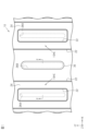
- FIG. 1 is a schematic plan view of an exemplary nitride semiconductor device according to the first embodiment.
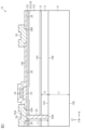
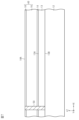
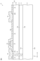
- FIG. 2 is a cross-sectional view taken along line 2-2 of FIG. 3A to 3C are schematic cross-sectional views illustrating exemplary manufacturing processes for the nitride semiconductor device according to the first embodiment.
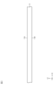
- FIG. 4 is a schematic cross-sectional view showing a manufacturing step subsequent to the step shown in FIG.
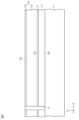
- FIG. 5 is a schematic cross-sectional view showing a manufacturing step subsequent to the step shown in FIG.
- FIG. 6 is a schematic cross-sectional view showing a manufacturing step subsequent to the step shown in FIG.
- FIG. 7 is a schematic cross-sectional view showing a manufacturing step subsequent to the step shown in FIG. FIG.
- FIG. 8 is a schematic cross-sectional view showing a manufacturing step subsequent to the step shown in FIG.
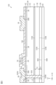
- FIG. 9 is a schematic cross-sectional view of an exemplary nitride semiconductor device according to the second embodiment.
- 10A to 10C are schematic cross-sectional views illustrating exemplary manufacturing processes for the nitride semiconductor device according to the second embodiment.
- FIG. 11 is a schematic cross-sectional view showing a manufacturing step subsequent to the step shown in FIG.
- FIG. 12 is a schematic cross-sectional view showing a manufacturing step subsequent to the step shown in FIG.
- FIG. 13 is a schematic cross-sectional view showing a manufacturing step subsequent to the step shown in FIG.
- FIG. 14 is a schematic cross-sectional view showing a manufacturing step subsequent to the step shown in FIG.
- 15A to 15C are schematic cross-sectional views showing a manufacturing process of a modified example subsequent to the process shown in FIG. 16A to 16C are schematic cross-sectional views showing a manufacturing process of the modified example subsequent to the process shown in FIG. 17A to 17C are schematic cross-sectional views showing a manufacturing process of the modified example subsequent to the process shown in FIG. 18A to 18C are schematic cross-sectional views showing a manufacturing process of the modified example subsequent to the process shown in FIG.
- FIG. 1 is a schematic plan view of an exemplary nitride semiconductor device 10 according to an embodiment.
- FIG. 2 is a schematic cross-sectional view of the nitride semiconductor device 10, taken along line 2-2 of FIG. 1.
- the term "plan view" used in the present disclosure refers to viewing the nitride semiconductor device 10 in the Z direction of the mutually orthogonal XYZ axes shown in FIG. 1 and FIG. 2.
- the +Z direction is defined as up, the -Z direction as down, the +X direction as right, and the -X direction as left in the nitride semiconductor device 10 shown in FIG. 1.
- the "plan view” refers to viewing the nitride semiconductor device 10 from above along the Z axis.
- the thickness refers to the dimension along the Z direction.
- the nitride semiconductor device 10 may be a HEMT using GaN.
- the cross-sectional structure of the nitride semiconductor device 10 will be described with reference to FIG. 2, and then the planar structure of the nitride semiconductor device 10 will be described with reference to FIG. 1.
- the nitride semiconductor device 10 includes a conductive substrate 12, a high-resistance layer 13 formed on the conductive substrate 12, a buffer layer 14 formed on the high-resistance layer 13, and a nitride semiconductor layer 40 formed on the buffer layer 14.
- the buffer layer 14 and the nitride semiconductor layer 40 are epitaxially grown on the upper surface 13A of the high-resistance layer 13.
- the nitride semiconductor layer 40 includes an electron transit layer 16 formed on the buffer layer 14, and an electron supply layer 18 formed on the electron transit layer 16.
- the conductive substrate 12 and the high-resistance layer 13 will be described in detail later.
- the buffer layer 14 is formed on the upper surface 13A of the high resistance layer 13.
- the buffer layer 14 may be located between the high resistance layer 13 and the electron transit layer 16.
- the buffer layer 14 may be made of any material that can facilitate epitaxial growth of the electron transit layer 16.
- the buffer layer 14 may include one or more nitride semiconductor layers.
- the thickness of the buffer layer 14 (when there are multiple buffer layers 14, the total thickness of the multiple buffer layers 14) is, for example, 50 nm or more and 1 ⁇ m or less.
- the buffer layer 14 may be omitted.
- the buffer layer 14 may include at least one of an aluminum nitride (AlN) layer, an aluminum gallium nitride (AlGaN) layer, and a graded AlGaN layer having different aluminum (Al) compositions.
- the buffer layer 14 may be composed of a single AlN layer, a single AlGaN layer, a layer having an AlGaN/GaN superlattice structure, a layer having an AlN/AlGaN superlattice structure, or a layer having an AlN/GaN superlattice structure.
- impurities may be introduced into a portion of the buffer layer 14 to make the buffer layer 14 semi-insulating.
- the impurity may be, for example, carbon (C) or iron (Fe), and the concentration of the impurity may be, for example, 4 ⁇ 10 16 cm ⁇ 3 or more.
- the electron travel layer 16 is made of a nitride semiconductor.
- the electron travel layer 16 is, for example, a GaN layer.
- the thickness of the electron travel layer 16 is, for example, 0.5 ⁇ m or more and 2 ⁇ m or less.
- an impurity may be introduced into a part of the electron travel layer 16 to make the electron travel layer 16 semi-insulating except for the surface layer region.
- the impurity is, for example, C
- the peak concentration of the impurity in the electron travel layer 16 is, for example, 1 ⁇ 10 19 cm ⁇ 3 or more.
- the electron supply layer 18 is made of a nitride semiconductor having a larger band gap than the electron transit layer 16.
- the electron supply layer 18 is, for example, an AlGaN layer.
- the electron supply layer 18 is made of Al x Ga 1-x N, where x is 0.1 ⁇ x ⁇ 0.4, and more preferably 0.2 ⁇ x ⁇ 0.3.
- the thickness of the electron supply layer 18 is, for example, 5 nm or more and 20 nm or less.
- the electron transit layer 16 and the electron supply layer 18 are composed of nitride semiconductors having different lattice constants. Therefore, the nitride semiconductor (e.g., GaN) constituting the electron transit layer 16 and the nitride semiconductor (e.g., AlGaN) constituting the electron supply layer 18 form a lattice-mismatched heterojunction.
- the energy level of the conduction band of the electron transit layer 16 near the heterojunction interface is lower than the Fermi level due to spontaneous polarization of the electron transit layer 16 and the electron supply layer 18 and piezoelectric polarization caused by stress experienced by the electron supply layer 18 near the heterojunction interface.
- 2DEG two-dimensional electron gas
- the nitride semiconductor device 10 further includes a gate layer 22 formed on the electron supply layer 18, a gate electrode 24 formed on the gate layer 22, and a passivation layer 26.
- the passivation layer 26 is formed on the electron supply layer 18, the gate layer 22, and the gate electrode 24, and includes a first opening 26A and a second opening 26B.
- the nitride semiconductor device 10 further includes a source electrode 28 that contacts the upper surface 18A of the electron supply layer 18 through the first opening 26A, a drain electrode 30 that contacts the upper surface 18A of the electron supply layer 18 through the second opening 26B, and a via 50.
- the via 50 will be described in detail later.
- the gate layer 22 is located between the first opening 26A and the second opening 26B of the passivation layer 26, and is spaced apart from each of the first opening 26A and the second opening 26B.
- the gate layer 22 is located closer to the first opening 26A than to the second opening 26B.
- the thickness of the gate layer 22 is, for example, 100 nm or more and 200 nm or less.
- the gate layer 22 has a smaller band gap than the electron supply layer 18 and is made of a nitride semiconductor containing acceptor-type impurities.
- the gate layer 22 can be made of any material that has a smaller band gap than the electron supply layer 18, which is, for example, an AlGaN layer.
- the gate layer 22 is a GaN layer doped with acceptor-type impurities (a p-type GaN layer).
- the acceptor-type impurities may include at least one of magnesium (Mg), zinc (Zn), and C.
- Mg magnesium
- Zn zinc
- C C
- Mg magnesium
- the maximum concentration of the acceptor-type impurities in the gate layer 22 is, for example, 1 ⁇ 10 18 cm ⁇ 3 or more, or 1 ⁇ 10 19 cm ⁇ 3 or more.
- the maximum concentration of the acceptor-type impurities in the gate layer 22 is, for example, 1 ⁇ 10 20 cm ⁇ 3 or less.
- the energy levels of the electron transit layer 16 and the electron supply layer 18 are raised by the inclusion of acceptor-type impurities in the gate layer 22. Therefore, in the region directly below the gate layer 22, the energy level of the conduction band of the electron transit layer 16 near the heterojunction interface between the electron transit layer 16 and the electron supply layer 18 is approximately the same as or higher than the Fermi level. Therefore, at zero bias when no voltage is applied to the gate electrode 24, 2DEG 20 is not formed in the electron transit layer 16 in the region directly below the gate layer 22. On the other hand, 2DEG 20 is formed in the electron transit layer 16 in regions other than the region directly below the gate layer 22.
- the presence of the gate layer 22 doped with acceptor-type impurities causes the 2DEG 20 to disappear in the region directly below the gate layer 22.
- the transistor operates normally off.
- an appropriate on-voltage is applied to the gate electrode 24, a channel is formed by the 2DEG 20 in the electron transit layer 16 in the region directly below the gate electrode 24, providing electrical continuity between the source and drain.
- the gate electrode 24 is composed of one or more metal layers.
- the gate electrode 24 is a titanium nitride (TiN) layer.
- the gate electrode 24 may be composed of a first metal layer formed of a material containing Ti and a second metal layer formed of a material containing TiN and stacked on the first metal layer.
- the gate electrode 24 can form a Schottky junction with the gate layer 22.
- the gate electrode 24 can be formed in an area smaller than the gate layer 22 in a plan view.
- the thickness of the gate electrode 24 is, for example, 50 nm or more and 200 nm or less.
- the passivation layer 26 is formed on the electron supply layer 18. It can be said that the passivation layer 26 covers the upper surface 18A of the electron supply layer 18.
- the passivation layer 26 can be made of a material containing any one of silicon nitride (SiN), silicon dioxide (SiO 2 ), silicon oxynitride (SiON), alumina (Al 2 O 3 ), AlN, and aluminum oxynitride (AlON).
- the passivation layer 26 is made of a material containing SiN.
- the portion of the passivation layer 26 covering the gate layer 22 and the gate electrode 24 has a non-flat surface because it is formed along the surfaces of the gate layer 22 and the gate electrode 24.
- the passivation layer 26 has a thickness of, for example, 200 nm or less.
- the thickness of the passivation layer 26 may be, for example, the thickness of the portion in contact with the electron supply layer 18, or the thickness of the portion in contact with the upper surface of the gate electrode 24.
- the source electrode 28 and the drain electrode 30 are disposed in the X direction on the upper surface 18A of the electron supply layer 18 so as to sandwich the gate layer 22.
- the source electrode 28 and the drain electrode 30 may be formed of one or more metal layers.
- the source electrode 28 and the drain electrode 30 may be formed of a combination of two or more metal layers selected from a group including a Ti layer, a TiN layer, an Al layer, an AlSiCu layer, and an AlCu layer.
- At least a portion of the source electrode 28 is filled in the first opening 26A and is in ohmic contact with the 2DEG 20 directly below the electron supply layer 18 through the first opening 26A.
- at least a portion of the drain electrode 30 is filled in the second opening 26B and is in ohmic contact with the 2DEG 20 directly below the electron supply layer 18 through the second opening 26B.
- the conductive substrate 12 has a substrate upper surface 12A and a substrate lower surface 12B facing the opposite side to the substrate upper surface 12A.
- the conductive substrate 12 has a resistance value of, for example, 2 ⁇ 10 ⁇ 2 ⁇ cm or less.
- An example of the conductive substrate 12 is a silicon carbide (SiC) substrate.
- the conductive substrate 12 may be doped with impurities.
- the impurities are, for example, nitrogen (N).
- the conductive substrate 12 is preferably polycrystalline, that is, a polycrystalline SiC substrate.
- the conductive substrate 12 may be doped with impurities or may be polycrystalline.
- the thickness T1 of the conductive substrate 12 is, for example, 50 ⁇ m or more, and preferably 100 ⁇ m or more.
- the thickness T1 of the conductive substrate 12 is, for example, 500 ⁇ m or less, and preferably 350 ⁇ m or less.
- the high resistance layer 13 has an upper surface 13A and a lower surface 13B facing the opposite side to the upper surface 13A.
- the lower surface 13B is a surface of the high resistance layer 13 facing the conductive substrate 12 side.
- the high resistance layer 13 is a layer for insulating between the conductive substrate 12 and the nitride semiconductor layer 40.
- the resistance value of the high resistance layer 13 is higher than the resistance value of the conductive substrate 12.
- the resistance value of the high resistance layer 13 is, for example, 1 ⁇ 10 5 ⁇ cm or more. In an example of a case where the buffer layer 14 is included, the resistance value of the high resistance layer 13 is higher than the resistance value of the buffer layer 14.
- the resistance value of the high resistance layer 13 is higher than the resistance value of the entire multiple buffer layers 14. In an example of a case where the buffer layer 14 is not included, the resistance value of the high resistance layer 13 is higher than the resistance value of the electron transit layer 16.
- the high resistance layer 13 can be formed of a semiconductor material such as Si, SiC, GaN, or sapphire.
- the high resistance layer 13 may be irradiated with an electron beam to achieve high resistance.
- An example of the high resistance layer 13 is a single crystal.
- the high resistance layer 13 is a single crystal SiC layer.
- An example of the high resistance layer 13 that is a single crystal SiC layer is a hexagonal SiC layer having an upper surface 13A that is inclined at an off angle of 2° to 6° with respect to the c-plane.
- the term "c-plane" is used to refer to the (0001) plane of a hexagonal SiC crystal.
- the off angle is preferably 3° to 5°, and more preferably 3.5° to 4.5°.
- the high-resistance layer 13 has a thermal expansion coefficient close to that of the conductive substrate 12.
- the difference between the thermal expansion coefficient of the conductive substrate 12 and the thermal expansion coefficient of the high-resistance layer 13 is 1 ⁇ 10 ⁇ 6 (1/° C.) or less. In this case, the occurrence of warping due to the difference in the thermal expansion coefficient between the high-resistance layer 13 and the conductive substrate 12 can be suppressed.
- a combination of a conductive substrate 12 and a high-resistance layer 13 made of the same material.
- Such combinations are, for example, a SiC substrate and a SiC layer, or a GaN substrate and a GaN layer.
- a combination of a conductive substrate 12 and a high-resistance layer 13 is a conductive substrate 12 that is a polycrystalline SiC substrate and a high-resistance layer 13 that is a single-crystalline SiC layer.
- the thickness T2 of the high resistance layer 13 is, for example, 100 ⁇ m or less, and preferably 20 ⁇ m or less. By reducing the thickness T2 of the high resistance layer 13, the length L1 of the via 50 described later can be shortened. Furthermore, the thickness T2 of the high resistance layer 13 is, for example, 3 ⁇ m or more. In one example, the thickness T2 of the high resistance layer 13 is thinner than the thickness T1 of the conductive substrate 12. The thickness T2 of the high resistance layer 13 may be thicker than the thickness T1 of the conductive substrate 12. Furthermore, in one example, the thickness T2 of the high resistance layer 13 is thinner than the thickness of the buffer layer 14 (if the buffer layer 14 is a multi-layer structure, the total thickness of the multi-layer structure). The thickness T2 of the high resistance layer 13 may be thicker than the thickness of the buffer layer 14.
- the via 50 is electrically connected to the source electrode 28, and also connects the source electrode 28 and the conductive substrate 12 in the Z direction.
- the electrode corresponding to the first electrode is the source electrode 28.
- a source voltage is applied to the conductive substrate 12 through the source electrode 28 and the via 50.
- the via 50 penetrates in the Z direction through the layers interposed between the source electrode 28 and the conductive substrate 12. More specifically, the via 50 penetrates in the Z direction through the high resistance layer 13, the buffer layer 14, the electron transit layer 16, and the electron supply layer 18.
- the lower end 50B of the via 50 contacts the substrate upper surface 12A of the conductive substrate 12.
- the upper end 50A of the via 50 contacts the source electrode 28.
- the shape and size of the via 50 are not particularly limited and can be changed as desired. Furthermore, the number of vias 50 is not particularly limited and may be either single or multiple.
- the length L1 of the via 50 is the total thickness (Z-direction dimension) of the layers interposed between the source electrode 28 and the conductive substrate 12 .
- the via 50 may be made of one or more conductive materials.
- the conductive material is, for example, a metal material including one or more appropriately selected from Ti, TiN, Au, Ag, Cu, Al, and W.
- One example of the via 50 is made of the same material as the source electrode 28. In this case, the via 50 and the source electrode 28 may be integrally formed, that is, may have no joint surface between them.
- FIG. 1 a planar structure of the nitride semiconductor device 10 will be described with reference to Fig. 1.
- the passivation layer 26 and the source electrode 28 are omitted, and a first opening 26A and a second opening 26B of the passivation layer 26 are depicted by dashed lines.
- the nitride semiconductor device 10 has, for example, active regions that contribute to transistor operation and inactive regions (not shown) that do not contribute to transistor operation.
- the active regions and inactive regions are arranged alternately in the Y direction.
- the source electrode 28 (see FIG. 2), the gate electrode 24, and the drain electrode 30 are arranged adjacent to each other in the X direction on the electron supply layer 18 (see FIG. 2).
- a combination of the source electrode 28, the gate electrode 24, and the drain electrode 30 adjacent to each other in the X direction constitutes one HEMT cell 10HC.
- two HEMT cells 10HC are arranged in the X direction in the active region. Note that in practice, more HEMT cells 10HC may be arranged in each active region.
- the manufacturing method of the nitride semiconductor device 10 includes a step of forming a conductive substrate 12 on a lower surface 13B of the high resistance layer 13.
- a plate-shaped member having a specific thickness and an upper surface 13A and a lower surface 13B is prepared as the high resistance layer 13.
- the member is, for example, a single crystal SiC substrate with an upper surface 13A inclined at an off angle of 2° or more and 6° or less with respect to the c-plane, and has a resistance value of 1 ⁇ 10 5 ⁇ cm or more.
- the conductive substrate 12 is, for example, a polycrystalline SiC substrate.
- the conductive substrate 12 can be formed on the high-resistance layer 13 using a chemical vapor deposition (CVD) method.
- CVD chemical vapor deposition
- a SiC film is formed on a layer containing one or both of graphene and hexagonal boron nitride on a substrate, and then the SiC film is peeled off from the substrate. The peeled off SiC film is used as the high-resistance layer 13, and a SiC layer constituting the conductive substrate 12 is formed on the surface of the SiC film.
- the temperature of the heat treatment can be determined according to the materials that make up the high resistance layer 13 and the semiconductor layer that will become the conductive substrate 12. For example, when the materials that make up the high resistance layer 13 and the semiconductor layer that will become the conductive substrate 12 are both SiC, the temperature of the heat treatment is 1500°C or higher, for example, about 1700°C.
- the method for manufacturing the nitride semiconductor device 10 includes the step of forming a buffer layer 14 and a nitride semiconductor layer 40 on the high-resistance layer 13 .
- a buffer layer 14, and an electron transit layer 16 and an electron supply layer 18 as a nitride semiconductor layer 40 are formed on an upper surface 13A of the high resistance layer 13.
- the electron transit layer 16 is formed on the buffer layer 14, and the electron supply layer 18 is formed on the electron transit layer 16.
- the buffer layer 14, the electron transit layer 16, and the electron supply layer 18 can be epitaxially grown on the high resistance layer 13 using the metal organic chemical vapor deposition (MOCVD) method.
- MOCVD metal organic chemical vapor deposition
- These layers are made of nitride semiconductors with relatively close lattice constants, so they can be epitaxially grown continuously.
- the buffer layer 14 is a multi-layer buffer layer, in which an AlN layer (first buffer layer) is formed on the high resistance layer 13, and then a graded AlGaN layer (second buffer layer) is formed on the AlN layer.
- the graded AlGaN layer is formed, for example, by stacking three AlGaN layers with Al compositions of 75%, 50%, and 25%, in that order, from the side closest to the AlN layer.
- the method for manufacturing the nitride semiconductor device 10 includes the step of forming a via 50 in the high-resistance layer 13, the buffer layer 14, and the nitride semiconductor layer 40.
- the step of forming the via 50 includes the step of forming a through hole 51 that penetrates the high-resistance layer 13, the buffer layer 14, and the nitride semiconductor layer 40, and the step of filling the through hole 51 with a conductive material.
- the through hole 51 is formed so as to penetrate the high resistance layer 13, the buffer layer 14, and the nitride semiconductor layer 40 and open to the upper surface of the nitride semiconductor layer 40 (upper surface 18A of the electron supply layer 18) and the lower surface 13B of the high resistance layer 13.
- the through hole 51 is formed by grinding the high resistance layer 13, the buffer layer 14, and the nitride semiconductor layer 40.
- the through hole 51 is formed by selectively removing a part of the high resistance layer 13, the buffer layer 14, and the nitride semiconductor layer 40 by lithography and etching.
- the through hole 51 is formed from the upper surface (upper surface 18A of the electron supply layer 18) side of the nitride semiconductor layer 40.
- the upper surface of the conductive substrate 12 is exposed to the through hole 51.
- a conductive material is filled in the through hole 51 to form a via 50.
- the method for manufacturing the nitride semiconductor device 10 includes the steps of forming a gate layer 22, forming a gate electrode 24, forming a passivation layer 26, forming a source electrode 28, and forming a drain electrode 30.
- the step of forming the source electrode 28 is a step of forming a first electrode on the nitride semiconductor layer 40.
- the gate layer 22 is formed by selectively removing a nitride semiconductor layer (not shown) formed on the electron supply layer 18 by lithography and etching.
- the nitride semiconductor layer can be epitaxially grown on the electron supply layer 18 by MOCVD.
- a doping gas is introduced into the growth chamber.
- Mg is doped as an acceptor-type impurity during the epitaxial growth of the nitride semiconductor layer. This allows the gate layer 22 containing the acceptor-type impurity to be formed.
- the gate electrode 24 is formed on the gate layer 22.
- the gate electrode 24 is formed by selectively removing a metal layer (not shown) formed on the nitride semiconductor layer 40 by lithography and etching.
- the passivation layer 26 is formed on the electron supply layer 18, the gate layer 22, and the gate electrode 24.
- the passivation layer 26 is formed so as to cover a portion of the electron supply layer 18, the gate layer 22, and the gate electrode 24.
- the passivation layer 26 can be formed using a low-pressure chemical vapor deposition (LPCVD) method.
- LPCVD low-pressure chemical vapor deposition
- a first opening 26A is formed to expose the electron supply layer 18 and the via 50, and a second opening 26B is formed to expose the electron supply layer 18.
- the first opening 26A and the second opening 26B are formed so that the gate layer 22 is located between the first opening 26A and the second opening 26B.
- the first opening 26A and the second opening 26B are formed by selectively removing a portion of the formed passivation layer 26 by lithography and etching.
- the source electrode 28 is formed so as to contact the upper surface 18A of the electron supply layer 18 exposed in the first opening 26A of the passivation layer 26 and the upper end 50A of the via 50.
- the drain electrode 30 is formed so as to contact the upper surface 18A of the electron supply layer 18 exposed in the second opening 26B of the passivation layer 26.
- the source electrode 28 and the drain electrode 30 are formed by selectively removing a metal layer (not shown) formed to cover the passivation layer 26 by lithography and etching. By going through each of the above steps, the nitride semiconductor device 10 can be obtained.
- the conductive substrate 12 has a low resistance value, and therefore functions as a back electrode to which a source voltage is applied through the source electrode 28 and the via 50.
- the high resistance layer 13 functions as an insulating layer that insulates the conductive substrate 12 from the nitride semiconductor layer 40 and the HEMT formed using the nitride semiconductor layer 40.
- the via 50 does not need to have a shape that penetrates the conductive substrate 12, but only needs to have a shape that contacts the conductive substrate 12.
- the length L1 of the via 50 can be shortened by the thickness of the conductive substrate 12. As a result of the shortening of the length L1 of the via 50, the cost, such as the amount of work and time required for forming the via 50, can be reduced.
- the stress of the nitride semiconductor layer 40 can be borne by the conductive substrate 12 and the high resistance layer 13. Therefore, even if the high resistance layer 13 is formed thin in order to shorten the length L1 of the via 50, it is easy to ensure the strength to resist the stress of the nitride semiconductor layer 40.
- the nitride semiconductor device 10 includes a conductive substrate 12 having a substrate upper surface 12A, a high resistance layer 13, a nitride semiconductor layer 40 formed on the high resistance layer 13, a first electrode (source electrode 28) formed on the nitride semiconductor layer 40, and a via 50.
- the high resistance layer 13 is formed on the substrate upper surface 12A and is a layer having a higher resistance value than the conductive substrate 12.
- the via 50 is electrically connected to the first electrode (source electrode 28), is provided penetrating the nitride semiconductor layer 40 and the high resistance layer 13, and is in contact with the substrate upper surface 12A.
- the length L1 of the via 50 can be shortened by the thickness of the conductive substrate 12.
- the cost such as the amount of work and time required to form the via 50
- the shortening of the length L1 of the via 50 reduces the contact area between the via 50 and the high resistance layer 13 and the nitride semiconductor layer 40. This makes it possible to reduce the ground inductance of the via 50. As a result, the effect of reducing deterioration of the nitride semiconductor device 10 can also be obtained.
- the difference between the thermal expansion coefficient of the conductive substrate 12 and the thermal expansion coefficient of the high resistance layer 13 is 1 ⁇ 10 ⁇ 6 (1/° C.) or less. In this case, the occurrence of warping due to the difference in the thermal expansion coefficient between the high resistance layer 13 and the conductive substrate 12 can be suppressed.
- the thickness T2 of the high resistance layer 13 is smaller than the thickness (T1) of the conductive substrate 12. In this case, the length of the via 50 penetrating the high resistance layer 13 in the thickness direction can be shortened. Therefore, the effect of (1-1) above can be obtained more significantly.
- the high-resistance layer 13 has an upper surface 13A facing the nitride semiconductor layer 40.
- the high-resistance layer 13 is a hexagonal single crystal SiC layer.
- the upper surface 13A of the high-resistance layer 13 is inclined at an off angle of 2° to 6° with respect to the c-plane. Since SiC substrates are generally expensive, the manufacturing cost of a nitride semiconductor device using a SiC substrate can be relatively high. Among SiC substrates, SiC substrates with an off angle are available relatively inexpensively.
- the nitride semiconductor device 100 of the second embodiment differs from the first embodiment in the configurations of the substrate 120, the high resistance layer 130, and the via 500.
- the nitride semiconductor device 100 of the second embodiment further includes a second electrode 60.
- the other configurations are similar to those of the first embodiment. In the following, a description of the components similar to those of the first embodiment will be omitted, and only components different from those of the first embodiment will be described.
- the substrate 120 has a substrate upper surface 120A and a substrate lower surface 120B facing the opposite side to the substrate upper surface 120A.
- the substrate 120 differs from the conductive substrate 12 of the first embodiment in terms of its configuration with respect to conductivity and thickness, but is otherwise similar in configuration to the conductive substrate 12.
- the substrate 120 may or may not be conductive.
- the resistance value of the substrate 120 may be 2 ⁇ 10 ⁇ 2 ⁇ cm or less, or may exceed 2 ⁇ 10 ⁇ 2 ⁇ cm.
- An example of the substrate 120 is a semiconductor substrate such as a Si substrate, a SiC substrate, a GaN substrate, or a sapphire substrate.
- the thickness T3 of the substrate 120 is, for example, 1 ⁇ m or more, and preferably 3 ⁇ m or more.
- the thickness T3 of the substrate 120 is, for example, 50 ⁇ m or less, and preferably 10 ⁇ m or less.
- the high resistance layer 130 has an upper surface 130A and a lower surface 130B facing the opposite side to the upper surface 130A.
- the lower surface 130B is the surface of the high resistance layer 130 facing the substrate 120.
- the resistance value of the high resistance layer 130 is higher than the resistance value of the substrate 120.
- the resistance value of the high resistance layer 130 is, for example, 1 ⁇ 10 5 ⁇ cm or more.
- the resistance value of the high resistance layer 130 is higher than the resistance value of the buffer layer 14.
- the resistance value of the high resistance layer 130 is higher than the overall resistance value of the multiple buffer layers 14.
- the resistance value of the high resistance layer 130 is higher than the resistance value of the electron transit layer 16.
- the thickness T4 of the high resistance layer 130 is, for example, 3 ⁇ m or more, and preferably 5 ⁇ m or more.
- the thickness T4 of the high resistance layer 130 is, for example, 100 ⁇ m or less, and preferably 20 ⁇ m or less.
- the length L2 of the via 500 described below can be shortened.
- the thickness T4 of the high resistance layer 130 is thicker than the thickness T3 of the substrate 120.
- the thickness T4 of the high resistance layer 130 may be thinner than the thickness T3 of the substrate 120.
- the thickness T4 of the high resistance layer 130 is thicker than the thickness of the buffer layer 14.
- the thickness T4 of the high resistance layer 130 may be thinner than the thickness of the buffer layer 14.
- the sum of the thickness T3 of the substrate 120 and the thickness T4 of the high resistance layer 130 is, for example, 4 ⁇ m or more, and preferably 8 ⁇ m or more.
- the sum of the thickness T3 of the substrate 120 and the thickness T4 of the high resistance layer 130 is, for example, 150 ⁇ m or less, and preferably 30 ⁇ m or less.
- the configuration of the high resistance layer 130 is the same as that of the high resistance layer 13 of the first embodiment.
- the second electrode 60 is formed on the bottom surface 120B of the substrate 120.
- the second electrode 60 has a top surface 60A and a bottom surface 60B facing the opposite side to the top surface 60A.
- the top surface 60A of the second electrode 60 faces the substrate 120.
- the second electrode 60 is electrically connected to the source electrode 28 through a via 500 described below.
- the second electrode 60 may be composed of one or more metal layers.
- the second electrode 60 may be composed of a combination of two or more metal layers selected from the group including, for example, a Ti layer, a TiN layer, an Au layer, an Al layer, an AlSiCu layer, and an AlCu layer.
- the thickness of the second electrode 60 is, for example, 3 ⁇ m or more and 50 ⁇ m or less.
- the via 500 is electrically connected to the source electrode 28 and also connects the source electrode 28 and the second electrode 60 in the Z direction.
- a source voltage is applied to the second electrode 60 through the source electrode 28 and the via 50.
- the via 500 penetrates the layer interposed between the source electrode 28 and the second electrode 60 in the Z direction.
- the via 500 penetrates the substrate 120, the high resistance layer 130, the buffer layer 14, the electron transit layer 16, and the electron supply layer 18 in the Z direction.
- the lower end 500B of the via 500 contacts the upper surface 60A of the second electrode 60.
- the upper end 500A of the via 500 contacts the source electrode 28.
- the shape and size of the via 500 are not particularly limited and can be changed as desired.
- the number of vias 500 is not particularly limited and may be either single or multiple.
- the length L2 of the via 500 is the total thickness (Z-direction dimension) of the layers interposed between the source electrode 28 and the second electrode 60.
- the configuration regarding the material constituting the via 500 is similar to that of the via 50 of the first embodiment.
- One example of the via 500 is made of the same material as one or both of the source electrode 28 and the second electrode 60.
- the via 500 may be formed integrally with one or both of the source electrode 28 and the second electrode 60 made of the same material, that is, the via 500 may be configured to have no joint surface between them.
- the method for manufacturing the nitride semiconductor device 100 includes a step of forming a buffer layer 14 and a nitride semiconductor layer 40 on the high-resistance layer 130. This step is the same as that of the first embodiment, except that the high-resistance layer 13 is changed to the high-resistance layer 130.
- the method for manufacturing the nitride semiconductor device 100 includes a step of forming a substrate 120 on the lower surface 130B of the high resistance layer 130.
- the method for forming the substrate 120 is the same as the method for forming the conductive substrate 12 in the first embodiment. Since it is easy to adjust the thickness of the substrate 120, it is preferable to form the substrate 120 by depositing a film using a CVD method.
- the method for manufacturing the nitride semiconductor device 100 includes the steps of forming a via 500 in the substrate 120, the high resistance layer 130, the buffer layer 14, and the nitride semiconductor layer 40.
- the step of forming the via 500 includes the steps of forming a through hole 510 that penetrates the substrate 120, the high resistance layer 130, the buffer layer 14, and the nitride semiconductor layer 40, and filling the through hole 510 with a conductive material.
- the through hole 510 is formed so as to penetrate the substrate 120, the high resistance layer 130, the buffer layer 14, and the nitride semiconductor layer 40, and to open to the upper surface of the nitride semiconductor layer 40 (upper surface 18A of the electron supply layer 18) and the substrate lower surface 120B of the substrate 120.
- the through hole 510 is formed by grinding the substrate 120, the high resistance layer 130, the buffer layer 14, and the nitride semiconductor layer 40.
- the through hole 510 is formed by selectively removing a part of the substrate 120, the high resistance layer 130, the buffer layer 14, and the nitride semiconductor layer 40 by lithography and etching.
- the through hole 510 may be formed from the substrate lower surface 120B side of the substrate 120, or from the upper surface of the nitride semiconductor layer 40 (upper surface 18A of the electron supply layer 18).
- a via 500 is formed by filling the through hole 510 with a conductive material.
- the method for manufacturing the nitride semiconductor device 100 includes a step of forming a second electrode 60 on the substrate underside 120B of the substrate 120.
- the second electrode 60 can be formed by forming a metal layer that becomes the second electrode 60 on the substrate underside 120B of the substrate 120.
- the method for manufacturing the nitride semiconductor device 100 includes the steps of forming a gate layer 22, forming a gate electrode 24, forming a passivation layer 26, forming a source electrode 28, and forming a drain electrode 30. Each of these steps is the same as in the first embodiment. By going through each of the above steps, the nitride semiconductor device 100 can be obtained.
- the substrate 120 and the high resistance layer 130 are interposed between the second electrode 60 connected to the source electrode 28 through the via 500 and the nitride semiconductor layer 40.
- the via 500 is formed to penetrate both the substrate 120 and the high resistance layer 130.
- interlayer thickness the thickness of the layer interposed between the second electrode 60 and the nitride semiconductor layer 40 (hereinafter referred to as interlayer thickness) can be easily adjusted.
- a HEMT is formed using the nitride semiconductor layer 40 and the nitride semiconductor layer 40 using a substrate that is thicker than the specified interlayer thickness. After that, the substrate is cut to obtain the specified interlayer thickness. Therefore, the interlayer thickness is adjusted by cutting the substrate.
- the substrate 120 having the second specified thickness is bonded to the lower surface 130B of the high resistance layer 130 having the first specified thickness, or the substrate 120 is formed by film deposition up to the second specified thickness. Therefore, the interlayer thickness (first specified thickness + second specified thickness) is adjusted by the work of newly forming the substrate 120. Adjusting the interlayer thickness by the work of newly forming the substrate 120 requires less work and shorter work time than adjusting the interlayer thickness by cutting the substrate. As a result, the cost required for manufacturing the nitride semiconductor device 100 having the via 500 can be reduced.
- the nitride semiconductor device 100 of the second embodiment has the same effects as those of (1-2) and (1-3) above. Furthermore, the nitride semiconductor device 100 of the second embodiment has the following effects.
- the nitride semiconductor device 100 includes a substrate 120 having a substrate upper surface 120A and a substrate lower surface 120B, a high resistance layer 130, a nitride semiconductor layer 40 formed on the high resistance layer 130, a source electrode 28 formed on the nitride semiconductor layer 40, a second electrode 60 formed under the substrate lower surface 120B of the substrate 120, and a via 500.
- the high resistance layer 130 is formed on the substrate upper surface 120A and has a higher resistance value than the substrate 120.
- the via 500 is provided penetrating the nitride semiconductor layer 40, the high resistance layer 130, and the substrate 120, and electrically connects the source electrode 28 and the second electrode 60.
- the cost required for adjusting the thickness (interlayer thickness) of the layer interposed between the second electrode 60 and the nitride semiconductor layer 40 can be reduced.
- the thickness T4 of the high resistance layer 130 is greater than the thickness T3 of the substrate 120. In this case, the time required for the process of forming the substrate 120 by film deposition on the lower surface 130B of the high resistance layer 130 can be further shortened. Therefore, the effect of (2-1) described above can be obtained more significantly.
- the first electrode connected to the conductive substrate 12 through the via 50 is not limited to the source electrode 28.
- the via 50 may be configured to electrically connect the drain electrode 30 and the conductive substrate 12.
- the first electrode is the drain electrode 30.
- a drain voltage is applied to the conductive substrate 12 through the drain electrode 30 and the via 50. The same applies to the via 500 of the nitride semiconductor device 100 of the second embodiment.
- the nitride semiconductor device 10 of the first embodiment may be a normally-on type that does not have the gate layer 22.
- the conductive substrate 12 of the nitride semiconductor device 10 of the first embodiment may be a metal substrate instead of a semiconductor substrate.
- the conductive substrate 12 is, for example, a Cu substrate, a molybdenum (Mo) substrate, a tantalum (Ta) substrate, a Ti substrate, a niobium (Nb) substrate, or a compound substrate including one or more of these substrates.
- the order of the steps is not limited to the order described in the embodiment, and can be changed as desired.
- the nitride semiconductor device 10 can be manufactured in the order shown in Figures 15 to 18.
- FIG. 15 shows a process subsequent to FIG. 3, in which a buffer layer 14 and a nitride semiconductor layer 40 are formed on the high-resistance layer 13.
- the buffer layer 14, and the electron transit layer 16 and the electron supply layer 18 as the nitride semiconductor layer 40 are formed on the upper surface 13A of the high-resistance layer 13.
- FIG. 16 and 17 show the process following FIG. 15, which is the process of forming a via 50.
- a through hole 51 is formed penetrating the high resistance layer 13, the buffer layer 14, and the nitride semiconductor layer 40.
- the through hole 51 may be formed from the lower surface 13B side of the high resistance layer 13, or from the upper surface (upper surface 18A of the electron supply layer 18) side of the nitride semiconductor layer 40.
- a conductive material is embedded in the through hole 51 to form the via 50.
- FIG. 18 shows a process following FIG. 17, in which a conductive substrate 12 is formed on the lower surface 13B of the high resistance layer 13.
- the process of forming the gate layer 22, the process of forming the gate electrode 24, the process of forming the passivation layer 26, the process of forming the source electrode 28, and the process of forming the drain electrode 30 are performed.
- the process of forming the conductive substrate 12 may be performed after the process of forming the gate layer 22, the process of forming the gate electrode 24, the process of forming the passivation layer 26, the process of forming the source electrode 28, and the process of forming the drain electrode 30.
- the conductive substrate 12 is a polycrystalline SiC substrate
- the process of filling the through hole 51 with a conductive material and the process of filling the source electrode 28 may be performed as a single process.
- the order of the steps may be changed.
- the step of forming the via 500 may be performed after the step of forming the second electrode 60.
- the step of forming the second electrode 60 may be performed after the steps of forming the gate layer 22, the step of forming the gate electrode 24, the step of forming the passivation layer 26, the step of forming the source electrode 28, and the step of forming the drain electrode 30.
- the process of filling the through hole 510 with a conductive material and the process of forming the source electrode 28 may be performed as a single process. Also, if the material constituting the via 500 is the same as the material constituting the second electrode 60, the process of filling the through hole 510 with a conductive material and the process of forming the second electrode 60 may be performed as a single process.
- a first layer is formed on a second layer is intended to mean that in some embodiments, the first layer may be placed directly on the second layer in contact with the second layer, while in other embodiments, the first layer may be placed above the second layer without contacting the second layer. In other words, the term “on” does not exclude a structure in which another layer is formed between the first and second layers.
- the Z direction used in this disclosure does not necessarily have to be the vertical direction, nor does it have to completely coincide with the vertical direction.
- the various structures according to this disclosure are not limited to the "up” and “down” of the Z direction described in this specification being “up” and “down” in the vertical direction.
- the X direction may be the vertical direction
- the Y direction may be the vertical direction.
- the conductive substrate (12) is a SiC substrate, The nitride semiconductor device (10) according to any one of appendices 1 to 3, wherein the high resistance layer (13) is a SiC layer.
- a buffer layer (14) is provided between the high resistance layer (13) and the nitride semiconductor layer (40), The nitride semiconductor device (10) according to any one of appendices 1 to 5, wherein the high resistance layer (13) has a resistance value higher than that of the buffer layer (14).
- a nitride semiconductor device (100) comprising:
- the substrate (120) is a SiC substrate;
- a buffer layer (14) is provided between the high resistance layer (130) and the nitride semiconductor layer (40), The nitride semiconductor device (100) according to any one of claims 9 to 12, wherein the high resistance layer (130) has a resistance value higher than that of the buffer layer (14).
- the high resistance layer (13, 130) has an upper surface (13A, 130A) facing the nitride semiconductor layer (40),
- the high resistance layer (13, 130) is a hexagonal single crystal SiC layer,
- the nitride semiconductor device (10, 100) according to any one of appendices 1 to 14, wherein the upper surface (13A, 130A) of the high resistance layer (13, 130) is inclined at an off angle of 2° or more and 6° or less with respect to a c-plane.
- the nitride semiconductor layer (40) is An electron transit layer (16) made of a nitride semiconductor; an electron supply layer (18) formed on the electron transit layer (16) and made of a nitride semiconductor having a band gap larger than that of the electron transit layer (16); a gate electrode (24), a source electrode (28), and a drain electrode (30) formed on the electron supply layer (18); Including, The nitride semiconductor device (10, 100) according to any one of appendices 1 to 15, wherein the via (50, 500) is electrically connected to the source electrode (28) as the first electrode.
Landscapes
- Junction Field-Effect Transistors (AREA)
Priority Applications (1)
| Application Number | Priority Date | Filing Date | Title |
|---|---|---|---|
| JP2025533950A JPWO2025018137A1 (https=) | 2023-07-18 | 2024-07-01 |
Applications Claiming Priority (2)
| Application Number | Priority Date | Filing Date | Title |
|---|---|---|---|
| JP2023-116837 | 2023-07-18 | ||
| JP2023116837 | 2023-07-18 |
Publications (1)
| Publication Number | Publication Date |
|---|---|
| WO2025018137A1 true WO2025018137A1 (ja) | 2025-01-23 |
Family
ID=94281880
Family Applications (1)
| Application Number | Title | Priority Date | Filing Date |
|---|---|---|---|
| PCT/JP2024/023790 Pending WO2025018137A1 (ja) | 2023-07-18 | 2024-07-01 | 窒化物半導体装置 |
Country Status (2)
| Country | Link |
|---|---|
| JP (1) | JPWO2025018137A1 (https=) |
| WO (1) | WO2025018137A1 (https=) |
Citations (4)
| Publication number | Priority date | Publication date | Assignee | Title |
|---|---|---|---|---|
| JP2004363563A (ja) * | 2003-05-15 | 2004-12-24 | Matsushita Electric Ind Co Ltd | 半導体装置 |
| JP2008536332A (ja) * | 2005-04-11 | 2008-09-04 | クリー インコーポレイテッド | 厚い半絶縁性または絶縁性エピタキシャル窒化ガリウム層およびそれを組み込んだデバイス |
| WO2022215583A1 (ja) * | 2021-04-08 | 2022-10-13 | ローム株式会社 | 窒化物半導体装置 |
| WO2023127520A1 (ja) * | 2021-12-27 | 2023-07-06 | ローム株式会社 | 窒化物半導体装置およびその製造方法 |
-
2024
- 2024-07-01 JP JP2025533950A patent/JPWO2025018137A1/ja active Pending
- 2024-07-01 WO PCT/JP2024/023790 patent/WO2025018137A1/ja active Pending
Patent Citations (4)
| Publication number | Priority date | Publication date | Assignee | Title |
|---|---|---|---|---|
| JP2004363563A (ja) * | 2003-05-15 | 2004-12-24 | Matsushita Electric Ind Co Ltd | 半導体装置 |
| JP2008536332A (ja) * | 2005-04-11 | 2008-09-04 | クリー インコーポレイテッド | 厚い半絶縁性または絶縁性エピタキシャル窒化ガリウム層およびそれを組み込んだデバイス |
| WO2022215583A1 (ja) * | 2021-04-08 | 2022-10-13 | ローム株式会社 | 窒化物半導体装置 |
| WO2023127520A1 (ja) * | 2021-12-27 | 2023-07-06 | ローム株式会社 | 窒化物半導体装置およびその製造方法 |
Also Published As
| Publication number | Publication date |
|---|---|
| JPWO2025018137A1 (https=) | 2025-01-23 |
Similar Documents
| Publication | Publication Date | Title |
|---|---|---|
| JP4525894B2 (ja) | 半導体素子形成用板状基体及びこの製造方法及びこれを使用した半導体素子 | |
| JP4381380B2 (ja) | 半導体装置及びその製造方法 | |
| US9954087B2 (en) | Field effect transistor, and multilayered epitaxial film for use in preparation of field effect transistor | |
| JP4744109B2 (ja) | 半導体装置とその製造方法 | |
| US8592823B2 (en) | Compound semiconductor device and method for manufacturing the same | |
| US9911842B2 (en) | Nitride semiconductor device, production method thereof, diode, and field effect transistor | |
| US12176430B2 (en) | Semiconductor structure and semiconductor device | |
| US20070210329A1 (en) | Warp-free semiconductor wafer, and devices using the same | |
| WO2010064362A1 (ja) | 電界効果トランジスタ | |
| JP2007059595A (ja) | 窒化物半導体素子 | |
| WO2013005372A1 (ja) | 半導体装置 | |
| JPWO2005015642A1 (ja) | 半導体装置及びその製造方法 | |
| JP2003059948A (ja) | 半導体装置及びその製造方法 | |
| JP2011166067A (ja) | 窒化物半導体装置 | |
| JP2012227456A (ja) | 半導体装置 | |
| JPWO2020174956A1 (ja) | 窒化物半導体装置 | |
| JP7216523B2 (ja) | 窒化物半導体装置 | |
| WO2023276972A1 (ja) | 窒化物半導体装置 | |
| US20240162165A1 (en) | Nitride semiconductor device and method for manufacturing the same | |
| JP2011108712A (ja) | 窒化物半導体装置 | |
| KR101172857B1 (ko) | 인헨스먼트 노멀리 오프 질화물 반도체 소자 및 그 제조방법 | |
| US20240347603A1 (en) | Nitride semiconductor device and method for manufacturing the same | |
| JP5415668B2 (ja) | 半導体素子 | |
| WO2025018137A1 (ja) | 窒化物半導体装置 | |
| US12336207B2 (en) | Semi-conductor structure and manufacturing method thereof |
Legal Events
| Date | Code | Title | Description |
|---|---|---|---|
| ENP | Entry into the national phase |
Ref document number: 2025533950 Country of ref document: JP Kind code of ref document: A |
|
| WWE | Wipo information: entry into national phase |
Ref document number: 2025533950 Country of ref document: JP |
|
| NENP | Non-entry into the national phase |
Ref country code: DE |