WO2025017437A1 - 処理装置及び表示システム - Google Patents
処理装置及び表示システム Download PDFInfo
- Publication number
- WO2025017437A1 WO2025017437A1 PCT/IB2024/056780 IB2024056780W WO2025017437A1 WO 2025017437 A1 WO2025017437 A1 WO 2025017437A1 IB 2024056780 W IB2024056780 W IB 2024056780W WO 2025017437 A1 WO2025017437 A1 WO 2025017437A1
- Authority
- WO
- WIPO (PCT)
- Prior art keywords
- circuit
- memory
- image data
- function
- memory cell
- Prior art date
- Legal status (The legal status is an assumption and is not a legal conclusion. Google has not performed a legal analysis and makes no representation as to the accuracy of the status listed.)
- Pending
Links
Images





































Classifications
-
- G—PHYSICS
- G06—COMPUTING OR CALCULATING; COUNTING
- G06F—ELECTRIC DIGITAL DATA PROCESSING
- G06F12/00—Accessing, addressing or allocating within memory systems or architectures
-
- G—PHYSICS
- G09—EDUCATION; CRYPTOGRAPHY; DISPLAY; ADVERTISING; SEALS
- G09F—DISPLAYING; ADVERTISING; SIGNS; LABELS OR NAME-PLATES; SEALS
- G09F9/00—Indicating arrangements for variable information in which the information is built-up on a support by selection or combination of individual elements
-
- G—PHYSICS
- G09—EDUCATION; CRYPTOGRAPHY; DISPLAY; ADVERTISING; SEALS
- G09F—DISPLAYING; ADVERTISING; SIGNS; LABELS OR NAME-PLATES; SEALS
- G09F9/00—Indicating arrangements for variable information in which the information is built-up on a support by selection or combination of individual elements
- G09F9/30—Indicating arrangements for variable information in which the information is built-up on a support by selection or combination of individual elements in which the desired character or characters are formed by combining individual elements
-
- G—PHYSICS
- G09—EDUCATION; CRYPTOGRAPHY; DISPLAY; ADVERTISING; SEALS
- G09G—ARRANGEMENTS OR CIRCUITS FOR CONTROL OF INDICATING DEVICES USING STATIC MEANS TO PRESENT VARIABLE INFORMATION
- G09G3/00—Control arrangements or circuits, of interest only in connection with visual indicators other than cathode-ray tubes
- G09G3/20—Control arrangements or circuits, of interest only in connection with visual indicators other than cathode-ray tubes for presentation of an assembly of a number of characters, e.g. a page, by composing the assembly by combination of individual elements arranged in a matrix no fixed position being assigned to or needed to be assigned to the individual characters or partial characters
-
- G—PHYSICS
- G09—EDUCATION; CRYPTOGRAPHY; DISPLAY; ADVERTISING; SEALS
- G09G—ARRANGEMENTS OR CIRCUITS FOR CONTROL OF INDICATING DEVICES USING STATIC MEANS TO PRESENT VARIABLE INFORMATION
- G09G3/00—Control arrangements or circuits, of interest only in connection with visual indicators other than cathode-ray tubes
- G09G3/20—Control arrangements or circuits, of interest only in connection with visual indicators other than cathode-ray tubes for presentation of an assembly of a number of characters, e.g. a page, by composing the assembly by combination of individual elements arranged in a matrix no fixed position being assigned to or needed to be assigned to the individual characters or partial characters
- G09G3/22—Control arrangements or circuits, of interest only in connection with visual indicators other than cathode-ray tubes for presentation of an assembly of a number of characters, e.g. a page, by composing the assembly by combination of individual elements arranged in a matrix no fixed position being assigned to or needed to be assigned to the individual characters or partial characters using controlled light sources
- G09G3/30—Control arrangements or circuits, of interest only in connection with visual indicators other than cathode-ray tubes for presentation of an assembly of a number of characters, e.g. a page, by composing the assembly by combination of individual elements arranged in a matrix no fixed position being assigned to or needed to be assigned to the individual characters or partial characters using controlled light sources using electroluminescent panels
- G09G3/32—Control arrangements or circuits, of interest only in connection with visual indicators other than cathode-ray tubes for presentation of an assembly of a number of characters, e.g. a page, by composing the assembly by combination of individual elements arranged in a matrix no fixed position being assigned to or needed to be assigned to the individual characters or partial characters using controlled light sources using electroluminescent panels semiconductive, e.g. using light-emitting diodes [LED]
- G09G3/3208—Control arrangements or circuits, of interest only in connection with visual indicators other than cathode-ray tubes for presentation of an assembly of a number of characters, e.g. a page, by composing the assembly by combination of individual elements arranged in a matrix no fixed position being assigned to or needed to be assigned to the individual characters or partial characters using controlled light sources using electroluminescent panels semiconductive, e.g. using light-emitting diodes [LED] organic, e.g. using organic light-emitting diodes [OLED]
- G09G3/3225—Control arrangements or circuits, of interest only in connection with visual indicators other than cathode-ray tubes for presentation of an assembly of a number of characters, e.g. a page, by composing the assembly by combination of individual elements arranged in a matrix no fixed position being assigned to or needed to be assigned to the individual characters or partial characters using controlled light sources using electroluminescent panels semiconductive, e.g. using light-emitting diodes [LED] organic, e.g. using organic light-emitting diodes [OLED] using an active matrix
-
- G—PHYSICS
- G09—EDUCATION; CRYPTOGRAPHY; DISPLAY; ADVERTISING; SEALS
- G09G—ARRANGEMENTS OR CIRCUITS FOR CONTROL OF INDICATING DEVICES USING STATIC MEANS TO PRESENT VARIABLE INFORMATION
- G09G3/00—Control arrangements or circuits, of interest only in connection with visual indicators other than cathode-ray tubes
- G09G3/20—Control arrangements or circuits, of interest only in connection with visual indicators other than cathode-ray tubes for presentation of an assembly of a number of characters, e.g. a page, by composing the assembly by combination of individual elements arranged in a matrix no fixed position being assigned to or needed to be assigned to the individual characters or partial characters
- G09G3/22—Control arrangements or circuits, of interest only in connection with visual indicators other than cathode-ray tubes for presentation of an assembly of a number of characters, e.g. a page, by composing the assembly by combination of individual elements arranged in a matrix no fixed position being assigned to or needed to be assigned to the individual characters or partial characters using controlled light sources
- G09G3/30—Control arrangements or circuits, of interest only in connection with visual indicators other than cathode-ray tubes for presentation of an assembly of a number of characters, e.g. a page, by composing the assembly by combination of individual elements arranged in a matrix no fixed position being assigned to or needed to be assigned to the individual characters or partial characters using controlled light sources using electroluminescent panels
- G09G3/32—Control arrangements or circuits, of interest only in connection with visual indicators other than cathode-ray tubes for presentation of an assembly of a number of characters, e.g. a page, by composing the assembly by combination of individual elements arranged in a matrix no fixed position being assigned to or needed to be assigned to the individual characters or partial characters using controlled light sources using electroluminescent panels semiconductive, e.g. using light-emitting diodes [LED]
- G09G3/3208—Control arrangements or circuits, of interest only in connection with visual indicators other than cathode-ray tubes for presentation of an assembly of a number of characters, e.g. a page, by composing the assembly by combination of individual elements arranged in a matrix no fixed position being assigned to or needed to be assigned to the individual characters or partial characters using controlled light sources using electroluminescent panels semiconductive, e.g. using light-emitting diodes [LED] organic, e.g. using organic light-emitting diodes [OLED]
- G09G3/3225—Control arrangements or circuits, of interest only in connection with visual indicators other than cathode-ray tubes for presentation of an assembly of a number of characters, e.g. a page, by composing the assembly by combination of individual elements arranged in a matrix no fixed position being assigned to or needed to be assigned to the individual characters or partial characters using controlled light sources using electroluminescent panels semiconductive, e.g. using light-emitting diodes [LED] organic, e.g. using organic light-emitting diodes [OLED] using an active matrix
- G09G3/3233—Control arrangements or circuits, of interest only in connection with visual indicators other than cathode-ray tubes for presentation of an assembly of a number of characters, e.g. a page, by composing the assembly by combination of individual elements arranged in a matrix no fixed position being assigned to or needed to be assigned to the individual characters or partial characters using controlled light sources using electroluminescent panels semiconductive, e.g. using light-emitting diodes [LED] organic, e.g. using organic light-emitting diodes [OLED] using an active matrix with pixel circuitry controlling the current through the light-emitting element
-
- G—PHYSICS
- G09—EDUCATION; CRYPTOGRAPHY; DISPLAY; ADVERTISING; SEALS
- G09G—ARRANGEMENTS OR CIRCUITS FOR CONTROL OF INDICATING DEVICES USING STATIC MEANS TO PRESENT VARIABLE INFORMATION
- G09G3/00—Control arrangements or circuits, of interest only in connection with visual indicators other than cathode-ray tubes
- G09G3/20—Control arrangements or circuits, of interest only in connection with visual indicators other than cathode-ray tubes for presentation of an assembly of a number of characters, e.g. a page, by composing the assembly by combination of individual elements arranged in a matrix no fixed position being assigned to or needed to be assigned to the individual characters or partial characters
- G09G3/22—Control arrangements or circuits, of interest only in connection with visual indicators other than cathode-ray tubes for presentation of an assembly of a number of characters, e.g. a page, by composing the assembly by combination of individual elements arranged in a matrix no fixed position being assigned to or needed to be assigned to the individual characters or partial characters using controlled light sources
- G09G3/30—Control arrangements or circuits, of interest only in connection with visual indicators other than cathode-ray tubes for presentation of an assembly of a number of characters, e.g. a page, by composing the assembly by combination of individual elements arranged in a matrix no fixed position being assigned to or needed to be assigned to the individual characters or partial characters using controlled light sources using electroluminescent panels
- G09G3/32—Control arrangements or circuits, of interest only in connection with visual indicators other than cathode-ray tubes for presentation of an assembly of a number of characters, e.g. a page, by composing the assembly by combination of individual elements arranged in a matrix no fixed position being assigned to or needed to be assigned to the individual characters or partial characters using controlled light sources using electroluminescent panels semiconductive, e.g. using light-emitting diodes [LED]
- G09G3/3208—Control arrangements or circuits, of interest only in connection with visual indicators other than cathode-ray tubes for presentation of an assembly of a number of characters, e.g. a page, by composing the assembly by combination of individual elements arranged in a matrix no fixed position being assigned to or needed to be assigned to the individual characters or partial characters using controlled light sources using electroluminescent panels semiconductive, e.g. using light-emitting diodes [LED] organic, e.g. using organic light-emitting diodes [OLED]
- G09G3/3266—Details of drivers for scan electrodes
-
- G—PHYSICS
- G09—EDUCATION; CRYPTOGRAPHY; DISPLAY; ADVERTISING; SEALS
- G09G—ARRANGEMENTS OR CIRCUITS FOR CONTROL OF INDICATING DEVICES USING STATIC MEANS TO PRESENT VARIABLE INFORMATION
- G09G3/00—Control arrangements or circuits, of interest only in connection with visual indicators other than cathode-ray tubes
- G09G3/20—Control arrangements or circuits, of interest only in connection with visual indicators other than cathode-ray tubes for presentation of an assembly of a number of characters, e.g. a page, by composing the assembly by combination of individual elements arranged in a matrix no fixed position being assigned to or needed to be assigned to the individual characters or partial characters
- G09G3/22—Control arrangements or circuits, of interest only in connection with visual indicators other than cathode-ray tubes for presentation of an assembly of a number of characters, e.g. a page, by composing the assembly by combination of individual elements arranged in a matrix no fixed position being assigned to or needed to be assigned to the individual characters or partial characters using controlled light sources
- G09G3/30—Control arrangements or circuits, of interest only in connection with visual indicators other than cathode-ray tubes for presentation of an assembly of a number of characters, e.g. a page, by composing the assembly by combination of individual elements arranged in a matrix no fixed position being assigned to or needed to be assigned to the individual characters or partial characters using controlled light sources using electroluminescent panels
- G09G3/32—Control arrangements or circuits, of interest only in connection with visual indicators other than cathode-ray tubes for presentation of an assembly of a number of characters, e.g. a page, by composing the assembly by combination of individual elements arranged in a matrix no fixed position being assigned to or needed to be assigned to the individual characters or partial characters using controlled light sources using electroluminescent panels semiconductive, e.g. using light-emitting diodes [LED]
- G09G3/3208—Control arrangements or circuits, of interest only in connection with visual indicators other than cathode-ray tubes for presentation of an assembly of a number of characters, e.g. a page, by composing the assembly by combination of individual elements arranged in a matrix no fixed position being assigned to or needed to be assigned to the individual characters or partial characters using controlled light sources using electroluminescent panels semiconductive, e.g. using light-emitting diodes [LED] organic, e.g. using organic light-emitting diodes [OLED]
- G09G3/3275—Details of drivers for data electrodes
-
- H—ELECTRICITY
- H04—ELECTRIC COMMUNICATION TECHNIQUE
- H04N—PICTORIAL COMMUNICATION, e.g. TELEVISION
- H04N5/00—Details of television systems
- H04N5/66—Transforming electric information into light information
-
- H—ELECTRICITY
- H05—ELECTRIC TECHNIQUES NOT OTHERWISE PROVIDED FOR
- H05B—ELECTRIC HEATING; ELECTRIC LIGHT SOURCES NOT OTHERWISE PROVIDED FOR; CIRCUIT ARRANGEMENTS FOR ELECTRIC LIGHT SOURCES, IN GENERAL
- H05B33/00—Electroluminescent light sources
- H05B33/12—Light sources with substantially two-dimensional [2D] radiating surfaces
- H05B33/14—Light sources with substantially two-dimensional [2D] radiating surfaces characterised by the chemical or physical composition or the arrangement of the electroluminescent material, or by the simultaneous addition of the electroluminescent material in or onto the light source
-
- H—ELECTRICITY
- H10—SEMICONDUCTOR DEVICES; ELECTRIC SOLID-STATE DEVICES NOT OTHERWISE PROVIDED FOR
- H10K—ORGANIC ELECTRIC SOLID-STATE DEVICES
- H10K50/00—Organic light-emitting devices
-
- H—ELECTRICITY
- H10—SEMICONDUCTOR DEVICES; ELECTRIC SOLID-STATE DEVICES NOT OTHERWISE PROVIDED FOR
- H10K—ORGANIC ELECTRIC SOLID-STATE DEVICES
- H10K59/00—Integrated devices, or assemblies of multiple devices, comprising at least one organic light-emitting element covered by group H10K50/00
-
- H—ELECTRICITY
- H10—SEMICONDUCTOR DEVICES; ELECTRIC SOLID-STATE DEVICES NOT OTHERWISE PROVIDED FOR
- H10K—ORGANIC ELECTRIC SOLID-STATE DEVICES
- H10K59/00—Integrated devices, or assemblies of multiple devices, comprising at least one organic light-emitting element covered by group H10K50/00
- H10K59/10—OLED displays
-
- H—ELECTRICITY
- H10—SEMICONDUCTOR DEVICES; ELECTRIC SOLID-STATE DEVICES NOT OTHERWISE PROVIDED FOR
- H10K—ORGANIC ELECTRIC SOLID-STATE DEVICES
- H10K59/00—Integrated devices, or assemblies of multiple devices, comprising at least one organic light-emitting element covered by group H10K50/00
- H10K59/10—OLED displays
- H10K59/12—Active-matrix OLED [AMOLED] displays
Definitions
- One aspect of the present invention relates to a processing device and a display system.
- one aspect of the present invention is not limited to the above technical field.
- the technical field of the invention disclosed in this specification relates to an object, an operating method, or a manufacturing method.
- one aspect of the present invention relates to a process, a machine, a manufacture, or a composition of matter. Therefore, more specifically, examples of the technical field of one aspect of the present invention disclosed in this specification include semiconductor devices, display devices (including liquid crystal display devices), light-emitting devices, power storage devices, imaging devices, memory devices, signal processing devices, sensors, processing devices (including processors), electronic devices, systems, their operating methods, their manufacturing methods, and their inspection methods.
- one operation method is to compare image data of two consecutive frames, and if the image data is identical to each other, omit rewriting one image data to the other.
- Patent Document 1 describes an operating method in which image data of the nth frame (n here is an integer equal to or greater than 1) is stored in a first storage device, and the mth row of the n+1th frame (m here is an integer equal to or greater than 1) is stored in a second storage device, image data of the mth row of each of the nth and n+1th frames is read out, a comparison circuit is used to determine whether or not the image data match, and a write control circuit determines whether or not to write image data of the mth row of the n+1th frame to the mth row of the display unit based on the result of the determination.
- the first storage device rewrites the image data for each frame in sequence. In other words, even if the image data in the mth row of each of the nth and n+1th frames is the same, the image data in the mth row of the nth frame is rewritten to the mth row of the n+1th frame in the first storage device.
- the image data of the mth row of the n+1th frame read from the second memory device is input to the judgment circuit, and the judgment data generated by the judgment circuit is input to the write control circuit, so the writing speed (frame frequency) of image data to the display unit is affected not only by the read speed of the first memory device, but also by the processing time by the judgment circuit and the write control circuit.
- An object of one embodiment of the present invention is to provide a processing device capable of comparing image data between previous and subsequent frames.
- an object of one embodiment of the present invention is to provide a processing device with reduced power consumption.
- an object of one embodiment of the present invention is to provide a display system including the processing device.
- an object of one embodiment of the present invention is to provide a display system in which a decrease in frame frequency is suppressed.
- an object of one embodiment of the present invention is to provide a new processing device or a new display system.
- the problem of one embodiment of the present invention is not limited to the problem described above.
- the problem described above does not preclude the existence of other problems.
- the other problems are problems not mentioned in this section, which will be described below. Problems not mentioned in this section can be derived by a person skilled in the art from the description in the specification or drawings, etc., and can be appropriately extracted from these descriptions.
- one embodiment of the present invention solves at least one of the problems described above and other problems. Therefore, one embodiment of the present invention does not need to solve all of the problems described above and other problems.
- One aspect of the present invention is a processing device that solves the above problem and includes a first line memory, a second line memory, a frame memory, and a processing circuit.
- the frame memory is assumed to hold image data for the t-th frame (where t is an integer greater than or equal to 1).
- This image data can be displayed by pixel circuits with M rows and N columns (where M and N are both integers greater than or equal to 1).
- the frame memory holds image data for the 1st through Mth rows of the t-th frame.
- the first line memory also holds image data for the i-th row (where i is an integer between 1 and M) of the t+1-th frame sent from outside the processing device.
- the second line memory also holds the image data of the i-th row of the t-th frame read from the frame memory.
- the processing circuit compares the image data of the i-th row of the t+1th frame read from the first line memory with the image data of the i-th row of the t-th frame read from the second line memory. If the image data of the i-th row of the t+1th frame does not match the image data of the i-th row of the t-th frame in this comparison, the first line memory transmits the image data of the i-th row of the t+1th frame read to the frame memory, and the frame memory rewrites the image data of the i-th row of the t-th frame that it holds to the image data of the i-th row of the t+1th frame.
- the first line memory does not transmit the image data of the i-th row of the t+1th frame to the frame memory, and does not rewrite the image data from the image data of the i-th row of the t-th frame to the image data of the i-th row of the t+1th frame in the frame memory.
- One aspect of the present invention is a processing device including a first line memory, a second line memory, a frame memory, a processing circuit, and a memory circuit.
- the first line memory has a function of acquiring a first row of data of the first image data and holding the first row of data.
- the frame memory has a function of holding the second image data.
- the second line memory has a function of acquiring a second row of data of the second image data read from the frame memory and holding the second row of data.
- the processing circuit has a function of comparing the first row of data read from the first line memory with the second row of data read from the second line memory and outputting comparison data including a comparison result.
- the first line memory also has a function of acquiring comparison data from the processing circuit, and outputting the first row data to the frame memory when the comparison data includes a comparison result indicating that the first row data and the second row data do not match.
- the frame memory also has a function of rewriting the second row data it holds with the first row data sent from the first line memory.
- the memory circuit also has a function of acquiring comparison data from the processing circuit and holding the comparison data.
- one aspect of the present invention may be configured such that in the above (1), the processing circuit has N (here, N is an integer of 1 or more) exclusive NOR circuits and a NAND circuit including N input terminals.
- one of the N exclusive NOR circuits has a function of performing a first logical operation using the value of the jth column (where j is an integer between 1 and N) of the first row data read from the first line memory and the value of the jth column of the second row data read from the second line memory, and outputting the result of the first logical operation.
- the NAND circuit has a function of acquiring the N results of the first logical operations from each of the N input terminals, performing a second logical operation using the N results of the first logical operations, and generating comparison data.
- Another embodiment of the present invention is a display system including a display device and the processing device according to (1) above.
- the display device includes a first driver circuit, a second driver circuit, and a pixel circuit
- the processing device includes a signal processing circuit.
- the signal processing circuit has a function of acquiring the comparison data read out from the memory circuit and generating a control signal using the comparison data.
- the first drive circuit also has a function of performing a third logical operation using a control signal sent from the signal processing circuit and a selection signal for selecting a pixel circuit, and transmitting the result of the third logical operation to the pixel circuit.
- the second drive circuit also has a function of determining whether to transmit the first row data or the second row data to the pixel circuit according to the control signal sent from the signal processing circuit.
- the first driver circuit may include a decoder and a logical AND circuit.
- the decoder has a function of generating a selection signal and transmitting the selection signal to a first input terminal of the logical product circuit. It is also preferable that the signal processing circuit has a function of transmitting a control signal to a second input terminal of the logical product circuit. It is also preferable that the logical product circuit has a function of performing a third logical operation using the control signal and the selection signal and outputting the result of the third logical operation.
- the second driver circuit may include a holding circuit, a digital-to-analog conversion circuit, and a switch.
- an output terminal of the holding circuit is electrically connected to an input terminal of the digital-to-analog conversion circuit.
- a first terminal of the switch is electrically connected to an output terminal of the digital-to-analog conversion circuit
- a second terminal of the switch is electrically connected to the pixel circuit
- a control terminal of the switch is electrically connected to a wiring to which a control signal is transmitted.
- the frame memory has a function of transmitting data of the first row or data of the second row to an input terminal of the holding circuit.
- the second frame memory also reads out image data for the i-th row of the t-th frame and transmits it to the second line memory. At this time, the second frame memory can also transmit the image data for the i-th row of the t-th frame to the display device.
- the second line memory also holds the image data for the i-th row of the t-th frame that has been read out from the second frame memory.
- the processing circuit is comparing the image data of the i-th row of the t+1th frame read from the first line memory with the image data of the i-th row of the t-th frame read from the second line memory, the image data of the i-th row of the t-th frame can be transmitted from the second frame memory to the display device.
- the processing circuit has a function of comparing the data of the first row read from the first line memory with the data of the second row read from the second line memory, and outputting comparison data including a comparison result.
- the storage circuit has a function of acquiring the comparison data from the processing circuit and holding the comparison data.
- the processing circuit may include N (here, N is an integer of 1 or more) exclusive NOR circuits and a NAND circuit.
- one of the N exclusive NOR circuits has a function of performing a first logical operation using the value of the jth column (j is an integer between 1 and N) of the first row data read from the first line memory and the value of the jth column of the second row data read from the second line memory, and outputting the result of the first logical operation.
- the NAND circuit has a function of performing a second logical operation using the N results of the first logical operations from each of the N input terminals, and generating comparison data.
- the display device may include a first driver circuit, a second driver circuit, and a pixel circuit
- the processing device may include a signal processing circuit
- the signal processing circuit has a function of acquiring comparison data read out from the memory circuit and generating a control signal using the comparison data.
- the first drive circuit has a function of performing a third logical operation using a control signal transmitted from the signal processing circuit and a selection signal for selecting a pixel circuit, and transmitting the result of the third logical operation to the pixel circuit.
- the second drive circuit has a function of determining whether to transmit the first row data or the second row data to the pixel circuit according to the control signal transmitted from the signal processing circuit.
- the first driver circuit may include a decoder and a logical AND circuit.
- the decoder has a function of generating a selection signal and transmitting the selection signal to a first input terminal of the logical product circuit. It is also preferable that the signal processing circuit has a function of transmitting a control signal to a second input terminal of the logical product circuit. It is also preferable that the logical product circuit has a function of performing a third logical operation using the control signal and the selection signal and outputting the result of the third logical operation.
- the second driver circuit may include a holding circuit, a digital-to-analog conversion circuit, and a switch.
- an output terminal of the holding circuit is electrically connected to an input terminal of the digital-to-analog conversion circuit.
- a first terminal of the switch is electrically connected to an output terminal of the digital-to-analog conversion circuit.
- a second terminal of the switch is electrically connected to the pixel circuit.
- a control terminal of the switch is electrically connected to a wiring to which a control signal is transmitted.
- the first frame memory has a function of transmitting data of the first row or data of the second row to an input terminal of the holding circuit.
- One aspect of the present invention is a display system having a processing device and a display device.
- the processing device includes a frame memory, a storage circuit, and a processing circuit.
- the frame memory also includes a first memory cell and a second memory cell.
- it has a function of simultaneously executing a write operation from the first memory cell and a read operation from the second memory cell, and a function of simultaneously executing a read operation from the first memory cell and a read operation from the second memory cell.
- the second memory cell is assumed to hold image data for the t-th frame (where t is an integer equal to or greater than 1) in advance.
- the image data can be displayed by pixel circuits with M rows and N columns (where M and N are both integers equal to or greater than 1).
- the second memory cell holds image data for the 1st to Mth rows of the t-th frame.
- the first memory cell holds the t+1th frame of image data transmitted from outside the processing device. As described above, while the t+1th frame of image data is being held in the first memory cell, the tth frame of image data in the second memory cell can be output.
- One aspect of the present invention is a processing device including a frame memory, a memory circuit, and a processing circuit.
- the frame memory includes a first memory cell and a second memory cell.
- the frame memory has a function of overlapping a write operation on one of the first memory cell and the second memory cell and a read operation on the other of the first memory cell and the second memory cell.
- the frame memory has a function of overlapping a read operation on the first memory cell and a read operation on the second memory cell.
- the processing circuit has a function of comparing first image data read from the first memory cell with second image data read from the second memory cell, and outputting comparison data including a comparison result.
- the memory circuit has a function of acquiring the comparison data from the processing circuit and holding the comparison data.
- one aspect of the present invention may be configured such that in the above (11), the frame memory has a first selection circuit, a second selection circuit, and a third selection circuit, and each of the first memory cell and the second memory cell has a first transistor, a second transistor, and a capacitor.
- each of the first memory cell and the second memory cell it is preferable that one of the source and drain of the first transistor is electrically connected to one of the pair of terminals of the capacitive element and the gate of the second transistor. It is also preferable that the first selection circuit is electrically connected to the gate of the first transistor of the first memory cell. It is also preferable that the second selection circuit is electrically connected to the gate of the first transistor of the second memory cell. It is also preferable that the third selection circuit is electrically connected to the other of the pair of terminals of the first capacitive element of the first memory cell and the other of the pair of terminals of the first capacitive element of the second memory cell.
- one aspect of the present invention may be configured such that in the above (12), the processing circuit has N (here, N is an integer of 1 or more) exclusive NOR circuits and a NAND circuit including N input terminals.
- one of the N exclusive NOR circuits has a function of performing a first logical operation using the value of the jth column (where j is an integer between 1 and N) of the first image data read from the first memory cell and the value of the jth column of the second image data read from the second memory cell, and outputting the result of the first logical operation.
- the NAND circuit has a function of acquiring the results of the N first logical operations from each of the N input terminals, performing a second logical operation using the results of the N first logical operations, and generating comparison data.
- one aspect of the present invention is a display system including a display device and the processing device according to (11).
- the display device includes a first driver circuit, a second driver circuit, and a pixel circuit
- the processing device includes a signal processing circuit.
- the signal processing circuit has a function of acquiring comparison data read from the storage circuit and generating a control signal using the comparison data.
- the first driver circuit has a function of performing a third logical operation using a control signal transmitted from the signal processing circuit and a selection signal for selecting the pixel circuit, and transmitting a result of the third logical operation to the pixel circuit.
- the frame memory has a function of reading out the first image data from the first memory cell and transmitting the first image data to the second driver circuit while rewriting the second image data held in the second memory cell to the third image data.
- the second driver circuit has a function of determining whether or not to transmit the first image data to the pixel circuit in response to a control signal transmitted from the signal processing circuit.
- the first driver circuit may include a decoder and a logical AND circuit.
- the decoder has a function of generating a selection signal and transmitting the selection signal to a first input terminal of the logical product circuit. It is also preferable that the signal processing circuit has a function of transmitting a control signal to a second input terminal of the logical product circuit. It is also preferable that the logical product circuit has a function of performing a third logical operation using the control signal and the selection signal and outputting the result of the third logical operation.
- the second driver circuit may include a holding circuit, a digital-to-analog conversion circuit, and a switch.
- an output terminal of the holding circuit is electrically connected to an input terminal of the digital-to-analog conversion circuit.
- a first terminal of the switch is electrically connected to an output terminal of the digital-to-analog conversion circuit
- a second terminal of the switch is electrically connected to the pixel circuit
- a control terminal of the switch is electrically connected to a wiring to which a control signal is transmitted.
- the frame memory has a function of transmitting the first image data to the input terminal of the holding circuit.
- the memory circuits included in the processing devices described in (11) to (16) above may be replaced with two memory circuits, a first memory circuit and a second memory circuit. This allows the first memory circuit and the second memory circuit to write comparison data while the other of the first memory circuit and the second memory circuit reads out different comparison data.
- one of the N exclusive NOR circuits has a function of performing a first logical operation using the value of the jth column (where j is an integer between 1 and N) of the first image data read from the first memory cell and the value of the jth column of the second image data read from the second memory cell, and outputting the result of the first logical operation.
- the NAND circuit has a function of acquiring the results of the N first logical operations from each of the N input terminals, performing a second logical operation using the results of the N first logical operations, and generating first comparison data.
- image data of the mth row of the nth frame can be transmitted to the display device while comparing image data of the mth row of each of the nth frame and the n+1th frame. Therefore, even if the processing time of each circuit included in the processing device is long, image data can be transmitted to the display device during that processing time, thereby preventing a decrease in the frame frequency of the display system.
- One aspect of the present invention can provide a processing device capable of comparing image data between previous and subsequent frames. Or, one aspect of the present invention can provide a processing device with reduced power consumption. Or, one aspect of the present invention can provide a display system having the above processing device. Or, one aspect of the present invention can provide a display system in which a decrease in frame frequency is suppressed. Or, one aspect of the present invention can provide a new processing device or a new display system.
- the effects of one embodiment of the present invention are not limited to the above effects.
- the above effects do not preclude the existence of other effects.
- the other effects are described below and are not mentioned in this section. Effects not mentioned in this section can be derived by a person skilled in the art from the description in the specification or drawings, etc., and can be extracted appropriately from these descriptions.
- One embodiment of the present invention has at least one of the above effects and other effects. Therefore, one embodiment of the present invention may not have the above effects in some cases.
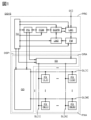
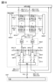
- FIG. 1 is a block diagram showing an example of the configuration of a display system.
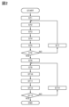
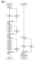
- FIG. 2 is a flowchart showing an example of the operation of the display system.
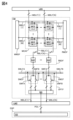
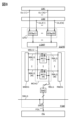
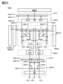
- FIG. 3 is a block diagram showing an example of the configuration of circuits included in the display system.
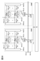
- FIG. 4 is a block diagram showing an example of the configuration of circuits included in the display system.
- FIG. 5 is a block diagram showing an example of the configuration of circuits included in the display system.
- FIG. 6 is a block diagram showing an example of the configuration of circuits included in the display system.
- FIG. 7 is a block diagram showing an example of the configuration of circuits included in the display system.
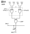
- 8A and 8B are circuit diagrams showing examples of the configuration of circuits included in the display system.
- FIG. 9A is a block diagram showing an example of the configuration of a circuit included in the display system
- FIG. 9B is a timing chart showing an example of the operation of the circuit included in the display system
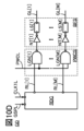
- 10A to 10D are circuit diagrams showing examples of the configuration of circuits included in the display system.
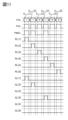
- FIG. 11 is a timing chart showing an example of the operation of the circuits included in the display system.
- FIG. 12 is a block diagram showing an example of the configuration of circuits included in the display system.
- FIG. 13 is a timing chart showing an example of the operation of the circuits included in the display system.
- FIG. 14 is a block diagram showing an example of the configuration of a display system.
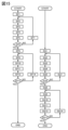
- FIG. 15 is a flowchart showing an example of the operation of the display system.
- FIG. 15 is a flowchart showing an example of the operation of the display system.
- FIG. 16 is a block diagram showing an example of the configuration of circuits included in the display system.
- FIG. 17 is a block diagram showing an example of the configuration of circuits included in the display system.
- FIG. 18 is a block diagram showing an example of the configuration of circuits included in the display system.
- FIG. 19 is a block diagram showing an example of the configuration of circuits included in the display system.
- FIG. 20 is a block diagram showing an example of the configuration of a display system.
- FIG. 21 is a flowchart showing an example of the operation of the display system.
- FIG. 22 is a block diagram showing an example of the configuration of circuits included in the display system.
- FIG. 23 is a block diagram showing an example of the configuration of circuits included in the display system.
- FIG. 24 is a timing chart showing an example of the operation of the circuits included in the display system.
- FIG. 25 is a timing chart showing an example of the operation of the circuits included in the display system.
- FIG. 26 is a block diagram showing an example of the configuration of circuits included in the display system.
- FIG. 27 is a block diagram showing an example of the configuration of a display system.
- FIG. 28 is a flowchart showing an example of the operation of the display system.
- FIG. 29 is a block diagram showing an example of the configuration of circuits included in the display system.
- FIG. 30 is a block diagram showing an example of the configuration of circuits included in the display system.
- FIG. 31 is a block diagram showing an example of the configuration of circuits included in the display system.
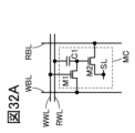
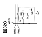
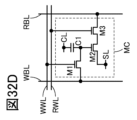
- 32A to 32F are circuit diagrams showing examples of the configuration of a memory cell.
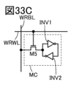
- 33A to 33F are circuit diagrams showing examples of the configuration of a memory cell.
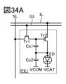
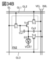
- 34A to 34D are circuit diagrams showing configuration examples of pixel circuits.
- 35A and 35B are circuit diagrams showing configuration examples of pixel circuits.
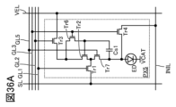
- 36A and 36B are circuit diagrams showing configuration examples of pixel circuits.
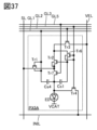
- FIG. 37 is a circuit diagram showing a configuration example of a pixel circuit.
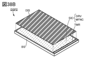
- 38A to 38C are schematic perspective views showing configuration examples of a display device.
- FIG. 39 is a block diagram showing an example of the configuration of a display device.
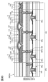
- FIG. 40 is a schematic cross-sectional view showing a configuration example of a display device.
- FIG. 41A is a schematic plan view showing a configuration example of a transistor
- FIGS. 41B and 41C are schematic cross-sectional views showing the configuration example of a transistor
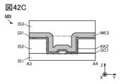
- FIG. 42A is a schematic plan view showing a configuration example of a transistor
- FIGS. 42B and 42C are schematic cross-sectional views showing the configuration example of a transistor
- 43A to 43C are schematic cross-sectional views showing examples of the configuration of a portion of a display device.
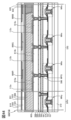
- FIG. 44 is a schematic cross-sectional view showing a configuration example of a display device.
- FIG. 45 is a schematic cross-sectional view showing a configuration example of a display device.
- FIG. 46 is a schematic cross-sectional view showing a configuration example of a display device.
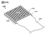
- 47A and 47B are diagrams showing a configuration example of a display module.
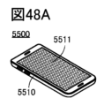
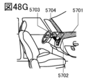
- 48A to 48I are diagrams showing an example of an electronic device.
- a semiconductor device is a device that utilizes semiconductor characteristics, and refers to a circuit including a semiconductor element (e.g., a transistor, a diode, and a photodiode), or a device having such a circuit.
- a semiconductor device also refers to any device that can function by utilizing semiconductor characteristics.
- An example of a semiconductor device is an integrated circuit.
- Another example of a semiconductor device is a chip including an integrated circuit, and another example of a semiconductor device is an electronic component that houses a chip in a package.
- a memory device, a display device, a light-emitting device, a lighting device, and an electronic device may themselves be semiconductor devices or may have a semiconductor device.
- one or more circuits that enable the functional connection between X and Y for example, logic circuits (for example, inverters, NAND circuits, and NOR circuits), signal conversion circuits (for example, digital-analog conversion circuits, analog-digital conversion circuits, and gamma correction circuits), potential level conversion circuits (for example, power supply circuits such as boost circuits or step-down circuits, and level shifter circuits that change the potential level of a signal), voltage sources, current sources, switching circuits, amplifier circuits (for example, circuits that can increase the signal amplitude or current amount, operational amplifiers, differential amplifier circuits, source follower circuits, and buffer circuits), signal generation circuits, memory circuits, and control circuits) can be connected between X and Y.
- logic circuits for example, inverters, NAND circuits, and NOR circuits
- signal conversion circuits for example, digital-analog conversion circuits, analog-digital conversion circuits, and gamma correction circuits
- potential level conversion circuits
- X and Y are electrically connected, this includes the case where X and Y are electrically connected (i.e., the case where X and Y are connected with another element or circuit between them) and the case where X and Y are directly connected (i.e., the case where X and Y are connected without another element or circuit between them).
- the source (e.g., sometimes referred to as one of the first terminal or the second terminal) and the drain (e.g., sometimes referred to as the other of the first terminal or the second terminal) of the transistor are electrically connected to each other, and are electrically connected in the order of X, the source of the transistor, the drain of the transistor, and Y.”
- the source of the transistor is electrically connected to X
- the drain of the transistor is electrically connected to Y
- X, the source of the transistor, the drain of the transistor, and Y are electrically connected in this order.
- one component may have the functions of multiple components.
- one conductive film has both the functions of wiring and the function of an electrode. Therefore, in this specification, the term "electrically connected" also includes such cases where one conductive film has the functions of multiple components.
- the term “resistance element” may be, for example, a circuit element having a resistance value higher than 0 ⁇ , or a wiring having a resistance value higher than 0 ⁇ . Therefore, in this specification, the term “resistance element” includes a wiring having a resistance value, a transistor in which a current flows between a source and a drain, a diode, or a coil. Therefore, the term “resistance element” may be rephrased as “resistance”, “load”, or “region having a resistance value”. Conversely, the term “resistance”, “load”, or “region having a resistance value” may be rephrased as “resistance element”.
- the resistance value may be, for example, preferably 1 m ⁇ or more and 10 ⁇ or less, more preferably 5 m ⁇ or more and 5 ⁇ or less, and even more preferably 10 m ⁇ or more and 1 ⁇ or less. It may also be, for example, 1 ⁇ or more and 1 ⁇ 10 9 ⁇ or less.
- a “capacitive element” can be, for example, a circuit element having a capacitance value higher than 0 F.
- a “capacitive element” (including a “capacitive element” with three or more terminals) includes an insulator and a pair of conductors sandwiching the insulator. Therefore, the term “pair of conductors" in a “capacitive element” can be rephrased as a “pair of electrodes," a “pair of conductive regions,” a “pair of regions,” or a “pair of terminals.”
- the terms “one of the pair of terminals” and “the other of the pair of terminals” may be referred to as a first terminal and a second terminal, respectively.
- the capacitance value can be, for example, 0.05 fF or more and 10 pF or less. It may also be, for example, 1 pF or more and 10 ⁇ F or less.
- parasitic capacitance examples include areas that contain different wirings with an insulator between them, and gate capacitance that occurs in transistors.
- capacitor element is explained as not including “parasitic capacitance.”
- a transistor has three terminals called a gate, a source, and a drain.
- the gate is a control terminal that controls the conductive state of the transistor.
- the two terminals that function as a source or a drain are input/output terminals of the transistor.
- One of the two input/output terminals becomes a source and the other becomes a drain depending on the conductivity type of the transistor (n-channel type or p-channel type) and the level of the potential applied to the three terminals of the transistor.
- the terms source and drain may be interchangeable.
- the terms “one of the source and drain” and “the other of the source and drain” are used.
- “one of the source and drain” may be referred to as "first terminal of the transistor” or “first electrode of the transistor”
- the other of the source and drain may be referred to as "second terminal of the transistor” or “second electrode of the transistor”.
- the transistor may have a backgate in addition to the three terminals described above.
- one of the gate or backgate of the transistor may be referred to as a first gate
- the other of the gate or backgate of the transistor may be referred to as a second gate.
- the terms "gate” and "backgate” may be interchangeable.
- the respective gates may be referred to as a first gate, a second gate, a third gate, etc.
- a transistor with a multi-gate structure having two or more gate electrodes can be used as an example of a transistor.
- the channel formation regions are connected in series, resulting in a structure in which multiple transistors are connected in series. Therefore, the multi-gate structure can reduce the off-current and improve the breakdown voltage of the transistor (improve reliability).
- the multi-gate structure when operating in the saturation region, even if the source-drain voltage changes, the drain current does not change much and a source-drain voltage-drain current characteristic with a flat slope can be obtained.
- the circuit element may have multiple circuit elements.
- two or more resistors directly connected in series may be expressed as one resistor.
- one capacitance element when one capacitance element is shown on a circuit diagram, this includes the case where two or more capacitance elements are directly connected in parallel.
- two or more capacitance elements directly connected in parallel may be expressed as one capacitance element.
- one transistor when one transistor is shown on a circuit diagram, this includes the case where two or more transistors are directly connected in series with their sources and drains connected together, and the gates of the respective transistors are directly connected together.
- a configuration in which two or more transistors are directly connected in series with their sources and drains connected together, and the gates of the respective transistors are directly connected together may be expressed as one transistor.
- a configuration in which the first terminals of two or more transistors are directly connected to each other, the second terminals of each transistor are directly connected to each other, and the gates of each transistor are directly connected to each other may be represented as one transistor.
- a switch refers to a device that can be in a conductive state (on state) or a non-conductive state (off state) and has the function of controlling whether or not a current flows.
- a switch refers to a device that has the function of selecting and switching the path through which a current flows.
- the switch may have two or more terminals for passing current in addition to the control terminal.
- an electrical switch, a mechanical switch, etc. may be used.
- the switch is not limited to a specific one as long as it has the function of controlling current.
- Examples of electrical switches include transistors (e.g., bipolar transistors, MOS transistors, etc.), diodes (e.g., PN diodes, PIN diodes, Schottky diodes, MIM (Metal Insulator Metal) diodes, MIS (Metal Insulator Semiconductor) diodes, and diode-connected transistors), or logic circuits that combine these.
- transistors e.g., bipolar transistors, MOS transistors, etc.
- diodes e.g., PN diodes, PIN diodes, Schottky diodes, MIM (Metal Insulator Metal) diodes, MIS (Metal Insulator Semiconductor) diodes, and diode-connected transistors
- the "conductive state" of the transistor refers to, for example, a state in which the source and drain of the transistor can be regarded as being electrically short-circuited, or a state in which a current can flow between the source and drain.
- the "non-conductive state" of the transistor refers to a state in which the source electrode and drain electrode of the transistor can be regarded as being electrically cut off. Note that when a transistor is operated simply as a switch, the polarity (conductivity type) of the transistor is not particularly limited.
- a mechanical switch is a switch that uses MEMS (microelectromechanical systems) technology.
- MEMS microelectromechanical systems
- This switch has an electrode that can be moved mechanically, and the movement of this electrode controls the conductive and non-conductive states.
- a node can be referred to as a terminal, wiring, electrode, conductive layer, conductor, or impurity region depending on the circuit configuration and device structure. Also, a terminal, wiring, etc. can be referred to as a node.
- Voltage refers to the potential difference from a reference potential, and if the reference potential is the ground potential, for example, then “voltage” can be interchanged with “potential.” Note that ground potential does not necessarily mean 0V. Potential is relative, and as the reference potential changes, the potential applied to wiring, the potential applied to circuits, etc., and the potential output from circuits, etc. also change.
- high-level potential and low-level potential do not refer to specific potentials. For example, if two wires are both described as “functioning as wires that supply a high-level potential,” the high-level potentials provided by both wires do not have to be equal to each other. Similarly, if two wires are both described as “functioning as wires that supply a low-level potential,” the low-level potentials provided by both wires do not have to be equal to each other.
- electrical current refers to the phenomenon of charge transfer (electrical conduction), and for example, the statement “electrical conduction of positively charged bodies is occurring” can be rephrased as “electrical conduction of negatively charged bodies is occurring in the opposite direction.” Therefore, in this specification, unless otherwise specified, “current” refers to the phenomenon of charge transfer (electrical conduction) accompanying the movement of carriers. Examples of carriers here include electrons, holes, anions, cations, and complex ions, and the carriers differ depending on the system through which the current flows (for example, semiconductors, metals, electrolytes, and vacuums). Furthermore, the "direction of current” in wiring, etc. is the direction in which positively charged carriers move, and is described as a positive current amount.
- the direction in which negatively charged carriers move is the opposite direction to the direction of current, and is expressed as a negative current amount. Therefore, in this specification, unless otherwise specified regarding the positive and negative of the current (or the direction of current), the statement “current flows from element A to element B” can be rephrased as “current flows from element B to element A.” Additionally, the statement “current is input to element A” can be rephrased as "current is output from element A.”
- ordinal numbers such as “first”, “second”, and “third” are used to avoid confusion of components. Therefore, they do not limit the number of components. Furthermore, they do not limit the order of components such as the process order or stacking order. Furthermore, even if a term does not have an ordinal number in this specification, an ordinal number may be added in the claims to avoid confusion of components. Furthermore, even if a term has an ordinal number in this specification, a different ordinal number may be added in the claims. Furthermore, even if a term has an ordinal number in this specification, the auxiliary number may be omitted in the claims.
- a component referred to by the ordinal number "first” in one embodiment of this specification may be a component referred to by a different ordinal number such as “second” or “third” in another embodiment or in the claims.
- a component referred to by the ordinal number "first” in one embodiment of this specification may be omitted in another embodiment or in the claims.
- the terms “above” and “below” indicating position may be used for convenience in order to explain the relative positions of components with reference to the drawings. Furthermore, the relative positions of components will change as appropriate depending on the direction in which each configuration is depicted. Therefore, it is not limited to the terms explained in the specification, etc., but can be rephrased appropriately depending on the situation. For example, the expression “insulator located on the upper surface of a conductor” can be rephrased as "insulator located on the lower surface of a conductor” by rotating the orientation of the drawing shown by 180 degrees.
- the terms “above” and “below” do not limit the positional relationship of components to being directly above or below and in direct contact.
- the expression “electrode B on insulating layer A” does not require that electrode B be formed in direct contact with insulating layer A, and does not exclude the inclusion of other components between insulating layer A and electrode B.
- the expression “electrode B above insulating layer A” does not require that electrode B be formed in direct contact with insulating layer A, and does not exclude the inclusion of other components between insulating layer A and electrode B.
- the expression “electrode B below insulating layer A” does not require that electrode B be formed in direct contact below insulating layer A, and does not exclude the inclusion of other components between insulating layer A and electrode B.
- the terms “row” and “column” may be used to describe components arranged in a matrix and their positional relationships. Furthermore, the positional relationships between components change as appropriate depending on the direction in which each configuration is depicted. Therefore, the terms are not limited to those described in the specification, etc., and can be rephrased appropriately depending on the situation. For example, the expression “row direction” can sometimes be rephrased as “column direction” by rotating the orientation of the shown drawing by 90 degrees. Similarly, the expression “column direction” can sometimes be rephrased as “row direction” by rotating the orientation of the shown drawing by 90 degrees.
- impurities in a semiconductor refers to, for example, anything other than the main component constituting the semiconductor layer.
- an element with a concentration of less than 0.1 atomic % is an impurity.
- the inclusion of impurities may result in one or more of the following: an increase in the density of defect levels in the semiconductor, a decrease in carrier mobility, and a decrease in crystallinity.
- impurities that change the characteristics of the semiconductor include, for example, Group 1 elements, Group 2 elements, Group 13 elements, Group 14 elements, Group 15 elements, and transition metals other than the main components, and in particular, for example, hydrogen (also included in water), lithium, sodium, silicon, boron, phosphorus, carbon, and nitrogen.
- Fig. 1 is a block diagram showing a configuration example of a display system according to one embodiment of the present invention.
- the display system DSYS shown in Fig. 1 includes, as an example, a display device DSP and a processing device PRC.
- the display device DSP also includes a pixel array unit PXA and a driving circuit unit DRA.
- the reference numerals of the multiple pixel circuits PX shown in FIG. 1 are accompanied by an address.
- the pixel circuit PX located in row 1, column 1 is illustrated as PX[1,1]
- the pixel circuit PX located in row M, column 1 is illustrated as PX[M,1]
- the pixel circuit PX located in row 1, column N is illustrated as PX[1,N]
- the pixel circuit PX located in row M, column N is illustrated as PX[M,N].
- the pixel circuit PX located in row i, column j (where i is an integer between 1 and M, and j is an integer between 1 and N) is referred to as pixel circuit PX[i,j] in this specification.
- the wiring GL[i] is connected to each of the pixel circuits PX[i,1] to PX[i,N].
- the wiring SL[j] is connected to each of the pixel circuits PX[1,j] to PX[M,j].
- Each of the wirings SL[1] to SL[N] functions as a wiring for transmitting an image signal, for example.
- Each of the wirings GL[1] to GL[M] functions as a wiring for transmitting a selection signal that selects the pixel circuit PX to which an image signal is written, for example.
- each of the wirings SL[1] to SL[N] is shown as a single wiring, but each of the wirings SL[1] to SL[N] can be considered as a wiring group in which two or more wirings are grouped together.
- each of the wirings GL[1] to GL[M] is shown as a single wiring, but each of the wirings GL[1] to GL[M] can be considered as a wiring group in which two or more wirings are grouped together.
- the drive circuit unit DRA includes, as an example, a drive circuit SD and a drive circuit GD.
- the driver circuit SD is connected to each of the wirings SL[1] to SL[N], for example.
- the driver circuit GD is connected to each of the wirings GL[1] to GL[M], for example.
- the drive circuit GD functions, for example, as a gate driver circuit for selecting pixel circuits PX to which an image signal is to be written.
- the drive circuit GD has the function of transmitting a selection signal to the wiring GL of the row to which the image signal is to be written, and transmitting a non-selection signal to the wiring GL of the row to which the image signal is not to be written.
- the drive circuit GD is sometimes called a selection circuit or a gate line selection circuit.
- the driving circuit GD also has a function of switching the selection signal sent to a specific row to a non-selection signal when the display image of the specific row does not change in the frames before and after the image displayed in the pixel array unit PXA. Whether or not the display image of the specific row changes is determined by a control signal generated by the signal processing circuit PG, which will be described later, and sent to the driving circuit GD.
- the drive circuit SD functions as a source driver circuit for transmitting image signals to the pixel circuits PX.
- the drive circuit SD also has a function of not transmitting an image signal of the second image to a specific row when the display images of the first image displayed in the pixel array unit PXA and the second image, which is the next frame of the first image, do not change.
- the drive circuit SD can operate so as not to rewrite the data of the first image written in the pixel circuits of the row with data of the second image.
- the drive circuit SD may have a function of making its output high impedance at the timing when the image signal of the second image to the row is not to be transmitted. Furthermore, the timing is determined by a control signal generated by the signal processing circuit PG, described later, and transmitted to the drive circuit SD.
- the processing device PRC has a memory circuit FM, a memory circuit LM1, a memory circuit LM2, a memory circuit FGM, a processing circuit SGPR, a signal processing circuit PG, and a control circuit TC.
- the memory circuit LM1 has a function as a first line memory. Specifically, for example, the memory circuit LM1 has a function of temporarily holding at least one row of image data for an image to be displayed in the pixel array unit PXA. Also, for example, the memory circuit LM1 has a function of acquiring image data D[i] (image data may be referred to as an image signal) to be transmitted to the i-th row of the pixel array unit PXA from outside the processing device PRC. Also, the memory circuit LM1 has a function of reading out the held image data D[i] and transmitting it to the processing circuit SGPR. Also, the memory circuit LM1 may have a function of reading out the held image data D[i] in accordance with comparison data (described later) transmitted from the processing circuit SGPR, and transmitting it to the memory circuit FM.
- image data image data may be referred to as an image signal
- the memory circuit LM2 has a function as a second line memory. Specifically, for example, like the memory circuit LM1, the memory circuit LM2 has a function of temporarily holding at least one row of image data for an image to be displayed in the pixel array unit PXA. Furthermore, it is preferable that the number of rows of image data that can be held in the memory circuit LM2 is equal to that of the memory circuit LM1. Furthermore, the memory circuit LM2, for example, has a function of acquiring image data D[i] from the memory circuit FM. Furthermore, the memory circuit LM2 has a function of reading out the held image data D[i] and transmitting it to the processing circuit SGPR.
- the processing circuit SGPR has a function of comparing a predetermined number of rows of image data read out from each of the memory circuits LM1 and LM2. Specifically, the processing circuit SGPR has a function of comparing the image data D[i] of the i-th row held in the memory circuits LM1 and LM2, respectively, and outputting comparison data C[i] as a result of the comparison and transmitting it to the memory circuit FGM. The processing circuit SGPR may also have a function of transmitting the comparison data C[i] to the memory circuit LM1.
- the memory circuit FGM has a function of holding the comparison data C[i] sent from the processing circuit SGPR, as an example.
- the memory circuit FGM can hold the comparison data C[1] to C[M] for the number of rows in the pixel array unit PXA.
- the memory circuit FGM also has a function of reading out the comparison data C[i] and sending it to the signal processing circuit PG.
- the memory circuit FGM is sometimes called a flag memory, since it holds the comparison data that determines whether or not to rewrite the image displayed in the pixel array unit PXA.
- the control circuit TC has a function of controlling each circuit included in the processing device PRC and each circuit included in the display device DSP.
- the control circuit TC has a function of transmitting command signals to the drive circuits included in each of the memory circuit LM1, memory circuit LM2, memory circuit FM, and memory circuit FGM to perform write operations, read operations, etc.
- the control circuit TC for example, has a function of transmitting command signals to the drive circuits SD and drive circuits GD to perform write operations, read operations, etc.
- the control circuit TC has a function of transmitting command signals to control the switching between the on state and the off state of the switching elements included in the memory circuit LM1, memory circuit LM2, memory circuit FM, memory circuit FGM, and processing circuit SGPR.
- the control circuit TC for example, has a function of generating clock signals to be supplied to each circuit included in the processing device PRC and each circuit included in the display device DSP.
- the control circuit TC may also have a function of transmitting a control signal generated by the signal processing circuit PG, a clock signal generated by the control circuit TC, or the like, as a synchronization signal to two or more selected circuits among the circuits included in the processing device PRC and the circuits included in the display device DSP, in order to synchronize the two or more selected circuits.
- the signal processing circuit PG for example, has a function of generating a control signal (sometimes called a pulse control signal) using the comparison data C[1] to C[M] sequentially read out from the memory circuit FGM.
- the signal processing circuit PG also has a function of transmitting the control signal to the drive circuit GD and the drive circuit SD.
- FIG. 2 is a flowchart showing an example of the operation of the display system DSYS in FIG. 1. This example of the operation includes steps ST1 to ST14.
- the flowchart in FIG. 2 shows the operation of rewriting the t-th frame image (where t is an integer equal to or greater than 1) that is pre-displayed in the pixel array unit PXA with the t+1-th frame image.
- image data D (t) [1] to D (t) [M] are stored in advance in the memory circuit FM as the t-th frame image.
- step ST1 as an example, the variable i for the row number of the pixel array unit PXA is set to 1.
- Step ST2 for example, includes an operation of transmitting image data D (t+1) [i] of the i-th row of the t+1th frame to the memory circuit LM1 from outside the processing device PRC.
- Step ST2 also includes an operation of writing the image data D (t+1) [i] to the memory circuit LM1.
- Step ST3 includes, as an example, an operation in which image data D (t+1) [i] is read out from the memory circuit LM1 and transmitted to the processing circuit SGPR.
- Step ST4 includes, for example, an operation of reading out image data D (t) [i] of the i-th row of the t-th frame from the memory circuit FM and transmitting it to the memory circuit LM2. It also includes an operation of reading out image data D (t) [i] from the memory circuit LM2 and transmitting it to the processing circuit SGPR.
- Step ST5 for example, includes an operation in which the processing circuit SGPR compares the image data D (t) [i] with the image data D (t+1) [i].
- Step ST5 also includes an operation in which, if the image data D (t) [i] and the image data D (t+1) [i] match, the processing circuit SGPR transmits comparison data C (t+1) [i] including a logic of "0" to the storage circuit FGM.
- Step ST5 also includes an operation in which, if the image data D (t) [i] and the image data D (t+1) [i] do not match, the processing circuit SGPR transmits comparison data C (t+1) [i] including a logic of "1" to the storage circuit FGM.
- comparison data C (t+1) [i] is just one example, and depending on the circuit configuration, for example, when image data D (t) [i] and image data D (t+1) [i] match, the comparison data C (t+1) [i] may include a logic of "1", and when image data D (t) [i] and image data D (t+1) [i] do not match, the comparison data C (t+1) [i] may include a logic of "0".
- step ST5 also includes, as an example, an operation of writing the comparison data C (t+1) [i] in the memory circuit FGM.
- step ST5 includes, as an example, an operation in which, when the comparison data C (t+1) [i] is "1", image data D (t+1) [i] is read from the memory circuit LM1 and transmitted to the memory circuit FM.
- the memory circuit FM performs an operation of rewriting the image data D (t) [i] held therein to the image data D (t+1) [i] read from the memory circuit LM1.
- the comparison data C (t+1) [i] is "0”
- the image data D (t+1) [i] may be read from the memory circuit LM1 and rewritten to the image data D (t) [i] held in the memory circuit FM.
- this operation can be regarded as a refresh operation of the image data D (t) [i] held in the memory circuit FM.
- image data D (t) [i] held in the memory circuit FM will be referred to as image data D (t+1) [i] regardless of whether the image data in the memory circuit FM has been rewritten or not.
- step ST6 it is determined whether i has reached M. If i has not reached M, the process moves from step ST6 to step ST7. If i has reached M, the process moves from step ST6 to step ST8.
- Step ST7 includes the operation of adding 1 to i. After adding 1 to i, the process returns to step ST2.
- step ST8 as an example, k is defined as a variable for the row number of the pixel array unit PXA. Also, in this step ST8, k is set to 1. Note that in steps ST8 to ST14, k is a variable that satisfies the range of 1 to M.
- step ST9 as an example, an operation is performed in which the comparison data C (t+1) [k] is read out from the memory circuit FGM and transmitted to the signal processing circuit PG.
- Step ST10 includes, as an example, an operation in which a logical operation is performed in the signal processing circuit PG between the continuous pulse signal and the comparison data C (t+ 1)[k] to generate a control signal including information on the comparison data C (t+1) [k].
- Step ST10 also includes, as an example, an operation in which the control signal is transmitted to the drive circuit GD and the drive circuit SD.
- logical operations please refer to the explanation of the configuration example of the signal processing circuit PG described later.
- Step ST11 includes an operation in which the image data D (t+1) [k] held in the memory circuit FM is read out and input to the drive circuit SD.
- Step ST12 includes an operation in which a logic operation is performed in the drive circuit GD on a selection signal with a logic of "1" sent to the kth row of the pixel array unit PXA and a control signal.
- the selection signal is converted into a non-selection signal (logic “0") with a logic of "0” as a result of the logic operation, and is sent to the wiring GL [k].
- the logic of the comparison data C (t+1) [k] is “1”
- the selection signal is not converted into a non-selection signal as a result of the logic operation, but is sent to the wiring GL [k] with a logic of "1".
- the drive circuit SD performs an operation of whether or not to make the output of the drive circuit SD high impedance in response to the control signal generated by the signal processing circuit PG. Specifically, when the logic of the comparison data C (t+1) [k] is "0", the drive circuit SD makes its output high impedance and does not output the image data D (t+1) [k]. Also, when the logic of the comparison data C (t+1) [k] is "1", the drive circuit SD outputs the image data D (t+1) [k].
- step ST13 it is determined whether k has reached M. If k has not reached M, the process moves from step ST13 to step ST14. If k has reached M, the present operation example ends.
- Step ST14 includes the operation of adding 1 to k. After adding 1 to k, the process moves back to step ST9.
- the image in the t+1th frame may be rewritten to the image in the t+2th frame by referring to the operation examples in steps ST1 to ST14.
- image data of previous and subsequent frames can be compared, and image data can be rewritten for rows in the pixel array section PXA that have been changed. This makes it possible to reduce the power consumption of the display system.
- each process or operation shown in the flowchart is classified by function and shown as a mutually independent step.
- it is difficult to separate the processes or operations shown in the flowchart by function and there may be cases where one step is involved in multiple steps, or one step is involved across multiple steps.
- the processes shown in the flowchart are not limited to the steps described in the specification, but can be appropriately rearranged depending on the situation. Specifically, the order of steps can be rearranged, and steps can be added and deleted depending on the situation and circumstances.
- the operating method of the processing device of one aspect of the present invention is not limited to the example operation of the flowchart of FIG. 2 above.
- steps ST1 to ST7 image data of previous and subsequent frames are compared, and the comparison data is written to the memory circuit FGM
- steps ST8 to ST14 the comparison data is read from the memory circuit FGM, a control signal is generated from the comparison data, and the image data is written to the display device.
- steps ST8 to ST14 can be performed simultaneously with all or part of the period in which steps ST1 to ST7 are performed.
- steps ST1 to ST7 the image data D (t+1) [i] and image data D (t+2) [i] are compared to obtain comparison data C (t+2) [i], and the comparison data C (t+2) [i] is written to the memory circuit FGM.
- steps ST8 to ST14 the comparison data C (t+1) [k] is read from the memory circuit FGM and the image data D (t+1) [i] is read from the memory circuit FM, and the image data D (t+1) [i] is written to the pixel array section PXA of the display device DSP based on the comparison data C (t+1) [k].
- the operating method of the processing device of one embodiment of the present invention or the operating method of the display system including the processing device can overlap a part or all of the periods of steps ST1 to ST7 and steps ST8 to ST14.
- This allows the comparison process of image data of the previous and next frames in steps ST1 to ST7 and the writing operation of image data to the display device in steps ST8 to ST14 to be performed simultaneously, thereby reducing the influence of the time required for the comparison process.
- the frame frequency of the display device can be increased.
- this configuration example shows an operation of rewriting the image of the t-th frame (where t is an integer equal to or greater than 1) that is already displayed in the pixel array unit PXA to the image of the t+1-th frame.
- image data D (t) [1] to D (t) [M] are stored in advance in the memory circuit FM as the t-th frame image.
- [Memory circuit LM1] 3 is a block diagram showing an example of the configuration of the memory circuit LM1.
- a processing circuit SGPR and a memory circuit FM are also shown in FIG.
- the memory circuit LM1 shown in FIG. 3 includes, as an example, a drive circuit WBD1, a drive circuit WWD1, a drive circuit RWD1, a drive circuit RBD1, a memory cell unit MCA1, and an output unit OPT1.
- the memory cell unit MCA1 has, as an example, a plurality of memory cells MC1. Also, in FIG. 3, as an example, N memory cells MC1 are arranged in one row in the memory cell unit MCA1. Note that in FIG. 3, the N memory cells MC1 may be arranged in the column direction instead of the row direction.
- each of the switches SW1A and SW1B is assumed to be a switch that turns on when a high-level potential is input to the control terminal, and turns off when a low-level potential is input to the control terminal. Furthermore, unless otherwise specified, all switches described in this specification, including the switches SW1A and SW1B, are assumed to be on when a high-level potential is input to the control terminal, and off when a low-level potential is input to the control terminal.
- the wiring SWL1B functions as a wiring for switching the switch SW1B included in the switching circuit SWC1 between the on state and the off state. Therefore, as an example, a high-level potential or a low-level potential is supplied to the wiring SWL1B as a signal for switching, similar to the wiring SWL1A.
- wirings OL1[1] to OL1[N] are shown as wirings for transmitting image data D (t+1) [i] from the memory circuit LM1 to the processing circuit SGPR, and wirings WBLF[1] to WBLF[N] are shown as wirings for transmitting image data D (t +1) [i] from the memory circuit LM1 to the memory circuit FM.
- Memory cell MCF[i,j] is, as an example, connected to wiring WBLF[j], wiring RBLF[j], wiring WWLF[i], and wiring RWLF[i].
- Each of the wirings WBLF[1] to WBLF[N] functions as, for example, a write data line, a write bit line, etc., in the memory cells MCF[i,1] to MCF[i,N] located in the i-th row of the memory circuit FM.
- image data D[i] read from the memory cell unit MCA1 of the memory circuit LM1 is transmitted to the wirings WBLF[1] to WBLF[N].
- the j-th column component of the image data D[i] is transmitted to the memory cell MCF[i] via the wiring WBLF[j].
- the description of the wirings RBL1[1] to RBL1[N] of the memory circuit LM1 can be referred to.
- the description of the wiring WWL1 of the memory circuit LM1 can be referred to.
- the description of the wiring RWL1 of the memory circuit LM1 can be referred to.
- the driving circuit WWDF for example, has a function of transmitting a write selection signal or non-selection signal to the wiring WWLF[i] when writing image data D[i] to the memory cells MCF[i,1] to MCF[i,N] in the i-th row of the memory cell unit MCAF.
- the driving circuit WWDF also has a function of transmitting a non-selection signal to the wirings WWLF[1] to WWLF[M] excluding the wiring WWLF[i] so as to prevent writing to each of the memory cells MCF[1,1] to MCF[M,N] in rows other than the i-th row of the memory cell unit MCAF.
- image data D[i] is transmitted from the memory circuit LM1 to the wirings WBLF[1] to WBLF[N], whereby the image data D[i] can be written to the memory cells MCF[i,1] to MCF[i,N] in the i-th row of the memory cell unit MCAF.
- the driving circuit RWDF has a function of transmitting a selection signal for reading to the wiring RWLF[i] when reading image data D[i] from the memory cells MCF[i,1] to MCF[i,N] in the i-th row of the memory cell unit MCAF, for example. It also has a function of transmitting a non-selection signal to the wirings RWLF[1] to RWLF[M] excluding the wiring RWLF[i] so that reading is not performed in each of the memory cells MCF[1,1] to MCF[M,N] in rows other than the i-th row of the memory cell unit MCAF.
- the driving circuit RWDF has a function as a read word line driver circuit in the memory cell unit MCAF, for example. Also, for the above reasons, the drive circuit WWDF is sometimes called a selection circuit.
- the drive circuit RWDF sends a read selection signal to the wiring RWLF[i] and sends a non-selection signal to the wirings RWLF[1] through RWLF[M] other than the wiring RWLF[i], thereby outputting a read potential corresponding to the image data D[i] from each of the memory cells MCF[i,1] through MCF[i,N] in the i-th row of the memory cell unit MCAF to each of the wirings RBLF[1] through RBLF[N].
- the description of the drive circuit RBDF can be referred to for the drive circuit RBD1 of the memory circuit LM1.
- the drive circuit RBDF has N sense amplifiers SAF as shown in FIG. 4.
- the sense amplifiers SAF can have a configuration similar to that of the sense amplifier SA1 shown in FIG. 3.
- the output unit OPTF has a function of selecting one of the memory circuit LM2 and the drive circuit SD, and transmitting image data D[i] read from the memory cells MCF[i,1] to MCF[i,N] to that one.
- the output section OPTF can be configured to have N switching circuits SWCF as shown in FIG. 4.
- each of the N switching circuits SWCF has a switch SWFA and a switch SWFB.
- switches applicable to the switches SW1A and SW1B of the memory circuit LM1 can be used for the switches SWFA and SWFB. Therefore, unless otherwise specified, the description of the switches SW1A and SW1B of the memory circuit LM1 can be referred to for the switches SWFA and SWFB.
- the output unit OPTF can be configured to have a switching circuit MX as shown in FIG. 4.
- the switching circuit MX has, as an example, N input terminals and one output terminal.
- the switching circuit MX has a function of making a state of conduction between one selected from the N input terminals and one output terminal, and making a state of non-conduction between the remaining input terminal and one output terminal.
- the switching circuit MX has a function as a multiplexer.
- the switching circuit MX can select data of one column out of N columns of the image data D[i] read out from the memory cell unit MCAF and output it to the output terminal of the switching circuit MX.
- the image data D[i] read out from the memory cell unit MCAF can be sequentially output to the wiring PDL column by column.
- the first terminal of the switch SWFA is connected to the sense amplifier SAF
- the second terminal of the switch SWFA is connected to the wiring WBL2[j]
- the control terminal of the switch SWFA is connected to the wiring SWLFA.
- the first terminal of the switch SWFB is connected to the sense amplifier SAF
- the second terminal of the switch SWFB is connected to one of the N input terminals of the switching circuit MX
- the control terminal of the switch SWFB is connected to the wiring SWLFB.
- each of the wirings WBL2[1] to WBL2[N] is connected to the memory circuit LM2. Furthermore, the output terminal of the switching circuit MX is connected to the wiring PDL.
- the wiring SWLFA functions as a wiring for switching the switch SWFA included in the switching circuit SWCF between the on state and the off state. Therefore, as an example, a high-level potential or a low-level potential is supplied to the wiring SWLFA as a signal for performing the switching.
- the wiring SWLFB functions as a wiring for switching the switch SWFB included in the switching circuit SWCF between the on state and the off state. Therefore, as an example, a high-level potential or a low-level potential is supplied to the wiring SWLFB as a signal for switching, similar to the wiring SWLFA.
- wirings WBL2[1] to WBL2[N] are shown as wirings for transmitting image data D[i] from the memory circuit FM to the memory circuit LM2, and wiring PDL is shown as wiring for transmitting image data D[i] from the memory circuit FM to the driver circuit SD.
- the memory circuit FM and the memory circuit LM2 are connected using multiple wirings WBL2[1] to WBL2[N], but a multiplexer may be provided in the memory circuit FM, a demultiplexer may be provided in the memory circuit LM2, and the multiplexer and the demultiplexer may be connected to each other.
- a multiplexer may be provided in the memory circuit FM
- a demultiplexer may be provided in the memory circuit LM2
- the multiplexer and the demultiplexer may be connected to each other.
- each of the second terminals of the multiple switches SWFB may be directly connected to the drive circuit SD. This allows the image data D[i] to be transmitted all at once, thereby shortening the time required to transmit the image data.
- [Memory circuit LM2] 5 is a block diagram showing an example of the configuration of the memory circuit LM2.
- a memory circuit FM and a processing circuit SGPR are also shown in FIG.
- the memory circuit LM2 shown in FIG. 5 includes, as an example, a drive circuit WWD2, a drive circuit RWD2, a drive circuit RBD2, a memory cell unit MCA2, and an output unit OPT2.
- Memory cell unit MCA2 has a plurality of memory cells MC2, for example. Also, in FIG. 5, as an example, in memory cell unit MCA2, N memory cells MC2 are arranged in a row, similar to memory cell unit MCA1. Note that in FIG. 3, the N memory cells MC2 may be arranged in a column direction instead of in a row direction.
- memory cell MC2 can be found in the description of memory cell MC1 in memory circuit LM1.
- memory cell MC2[j] is connected to wiring WBL2[j], wiring RBL2[j], wiring WWL2, and wiring RWL2.
- the wirings WBL2[1] to WBL2[N] function as write data lines, write bit lines, etc. in the memory cells MC2[1] to MC2[N] of the memory circuit LM2.
- image data D(t)[i] read from the memory cells MC[i,1] to MC[i,N] in the i-th row of the memory cell unit MCAF of the memory circuit FM is transmitted to the wirings WBL2[1] to WBL2[N].
- the j-th column component of the image data D ( t) [i] is transmitted to the memory cell MC2[i] via the wiring WBL2[j].
- the description of the wirings RBL1[1] to RBL1[N] of the memory circuit LM1 can be referred to.
- the description of the wiring WWL1 of the memory circuit LM1 can be referred to.
- the description of the wiring RWL1 of the memory circuit LM1 can be referred to.
- the explanation for the drive circuit WWD1 of the memory circuit LM1 can be referred to.Furthermore, for the drive circuit RWD2, unless otherwise specified, the explanation for the drive circuit RWD1 of the memory circuit LM1 can be referred to.
- the description of the drive circuit RBD2 can be referred to for the drive circuit RBD1 of the memory circuit LM1.
- the drive circuit RBD2 has N sense amplifiers SA2 as shown in FIG. 5.
- the sense amplifiers SA2 can be configured similarly to the sense amplifiers SA1 shown in FIG. 3, for example.
- the output unit OPT2 has a function of selecting whether or not to output the image data D[i] read from the memory cells MC2[1] to MC2[N] of the memory circuit LM2 to the wirings OL2[1] to OL2[N].
- the output unit OPT2 can be configured to have N switches SW2 as shown in FIG. 5.
- the switches SW2 for example, a switch applicable to the switches SW1A or SW1B of the memory circuit LM1 can be used. Therefore, unless otherwise specified, the description of the switches SW1A or SW1B of the memory circuit LM1 can be referred to for the switches SW2.
- Each of the wiring OL2[1] to OL2[N] is connected to the processing circuit SGPR.
- the wirings OL2[1] to OL2[N] are illustrated as wirings for transmitting image data D (t) [i] from the memory circuit LM2 to the processing circuit SGPR.
- the memory circuit LM2 and the processing circuit SGPR are connected using multiple wirings OL2[1] to OL2[N], but a multiplexer may be provided in the memory circuit LM2, a demultiplexer may be provided in the processing circuit SGPR, and the multiplexer and the demultiplexer may be connected to each other.
- a multiplexer may be provided in the memory circuit LM2
- a demultiplexer may be provided in the processing circuit SGPR
- the multiplexer and the demultiplexer may be connected to each other.
- FIG. 6 is a block diagram showing an example of the configuration of the processing circuit SGPR.
- a memory circuit LM1 a memory circuit LM2, a memory circuit FGM, and a signal processing circuit PG are also shown in FIG.
- the processing circuit SGPR shown in FIG. 6 includes, as an example, a comparison circuit CPA and a logic circuit LGMP. Also, as an example, the comparison circuit CPA includes comparators CPAa[1] through CPAa[N].
- Each of the comparators CPAa[1] to CPAa[N] has a first input terminal, a second input terminal, and an output terminal.
- the logic circuit LGMP also has N input terminals and one output terminal.
- the input terminal in the jth column is referred to as the jth input terminal.
- the first input terminal of the comparator CPAa[j] is connected to the wiring OL1[j]
- the second input terminal of the comparator CPAa[j] is connected to the wiring OL2[j].
- the output terminal of the comparator CPAa[j] is connected to the jth input terminal of the logic circuit LGMP.
- An output terminal of the logic circuit LGMP is connected to a wiring WBLG, which will be described later.
- the wiring WBLG is shown as a wiring for transmitting the comparison data C (t+1) [i] from the processing circuit SGPR to the memory circuit FGM.
- the logic circuit LGMP can be, for example, an AND circuit (logical product circuit), a NAND circuit (negated logical product circuit), an OR circuit (logical sum circuit), or a NOR circuit (negated logical sum circuit) having N input terminals.
- the information output from the logic circuit LGMP is referred to as comparison data.
- the image data D (t+1) [i] read from the memory circuit LM1 is transmitted from the wiring OL1
- the image data D (t) [i] read from the memory circuit LM2 is transmitted from the wiring OL2.
- the image data D (t) [i] and the image data D (t+1) [i] are input to the processing circuit SGPR to generate the comparison data C (t+1) [i].
- the comparison data C (t+1) [i] is transmitted from the processing circuit SGPR to the memory circuit FGM via the wiring WBLG.
- each of the comparators CPAa[1] to CPAa[N] is an XOR circuit (exclusive OR circuit) and the logic circuit LGMP is an OR circuit (logical OR circuit).
- the processing circuit SGPR may be provided with a switch SWP at the end of the output terminal of the logic circuit LGMP as shown in FIG. 8A.
- the switch SWP can be an output unit in the processing circuit SGPR in FIG. 8A.
- the output unit functions as a circuit or a circuit element that selects whether or not to transmit the comparison data C (t+1) [i] generated by the processing circuit SGPR to the wiring WBLG.
- the first terminal of the switch SWP is connected to the output terminal of the logic circuit LGMP, and the second terminal of the switch SWP is connected to the wiring WBLG described later.
- the control terminal of the switch SWP is connected to the wiring SWLP.
- a switch applicable to the switch SW1A or switch SW1B of the memory circuit LM1 can be used as the switch SWP. Therefore, unless otherwise specified, the description of the switch SW1A or switch SW1B of the memory circuit LM1 can be referred to for the switch SWP.
- the wiring SWLP functions as a wiring for switching the switch SWP included in the processing circuit SGPR between an on state and an off state. Therefore, as an example, a high-level potential or a low-level potential is supplied to the wiring SWLP as a signal for performing the switching.
- the processing circuit SGPR when the image data D (t+1) [i] transmitted from the memory circuit LM1 to the processing circuit SGPR matches the image data D (t) [i] transmitted from the memory circuit LM2 to the processing circuit SGPR, the processing circuit SGPR outputs "0" to the wiring WBLG as the "false” logic of the comparison data C (t+1 )[i]. Also, when the image data D(t+1) [i] transmitted from the memory circuit LM1 to the processing circuit SGPR does not match the image data D (t) [i] transmitted from the memory circuit LM2 to the processing circuit SGPR, the processing circuit SGPR outputs "1" to the wiring WBLG as the "true” logic of the comparison data C (t+1) [i].
- the circuit configuration in FIG. 8A is just an example, and the processing circuit SGPR in FIG. 6 may have the circuit configuration in FIG. 8B.
- the processing circuit SGPR shown in FIG. 8B is a modified example of the processing circuit SGPR in FIG. 8A, and differs from the processing circuit SGPR in FIG. 8A in that each of the comparators CPAa[1] to CPAa[N] is an NXOR circuit (exclusive negative OR circuit) and the logic circuit LGMP is a NAND circuit (negative AND circuit).
- the processing circuit SGPR of FIG. 8B similarly to the processing circuit SGPR of FIG. 8A, when the same data is input to the first input terminal and the second input terminal of all of the comparators CPAa[1] to CPAa[N] (for example, when the j-th column of the image data D (t) [i] and the j-th column of the image data D (t) [i] match), the logic of the comparison data C (t+1) [i] is output to the output terminal of the logic circuit LGMP as "0".
- the logic of the comparison data C (t+1) [i] is output to the output terminal of the logic circuit LGMP as "1".
- the wiring WBLG shown in Fig. 6 may be connected to the wiring SWL1B as shown in Fig. 7.
- the logic "0" of the comparison data C (t+1) [i] output from the output terminal of the logic circuit LGMP corresponds to a low level potential
- the logic "1" of the comparison data C (t+1) [i] output from the output terminal of the logic circuit LGMP corresponds to a high level potential
- the memory circuit FGM shown in FIG. 6 includes, as an example, a drive circuit WWDG, a drive circuit RWDG, a sense amplifier SAG, a memory cell unit MCAG, and a switch SWG.
- the memory cell unit MCAG has, as an example, a plurality of memory cells MCG. Also, in FIG. 6, as an example, M memory cells MCG are arranged in a column in the memory cell unit MCAG. Note that in FIG. 3, the M memory cells MCG may be arranged in the row direction instead of the column direction.
- the reference numerals of the multiple memory cells MCG shown in FIG. 6 are accompanied by an address.
- the memory cell MCG located in the first row is illustrated as MCG[1]
- the memory cell MCG located in the Mth row is illustrated as MCG[M].
- the memory cell MCG located in the i-th row is referred to as the memory cell MCG[i] in this specification.
- memory cell MCG unless otherwise specified, the description of memory cell MC1 in memory circuit LM1 can be referred to.
- Memory cell MCG[i] is connected to, for example, wiring WBLG, wiring RBLG, wiring WWLG[i], and wiring RWLG[i].
- wiring RBLG is connected to a sense amplifier SAG.
- the wiring WBLG functions as a write data line, a write bit line, etc. in the memory cell MCG[i]. Further, the comparison data C (t+1) [i] output from the logic circuit LGMP described above is transmitted to the wiring WBLG.
- wiring RBL1[1] to wiring RBL1[N] of memory circuit LM1 can be referred to.
- the description of wiring WWLG[1] to WWLG[M] can be referred to.
- the description of wiring RWLG[1] to RWLG[M] can be referred to.
- the driver circuit WWDG has a function of transmitting a selection signal for writing to the wiring WWLG[i] when writing the comparison data C (t+1) [i] to the memory cell MCG[i] of the memory cell unit MCAG.
- the driver circuit WWDG also has a function of transmitting a non-selection signal to the wirings WWLG[1] to WWLG[M] except the wiring WWLG[i] so as to prevent writing to each of the memory cells MCG[1] to MCG[M] in rows other than the i-th row of the memory cell unit MCAG.
- the memory cells MCG included in the memory cell unit MCAG can be sequentially selected for each row as the write destination of the comparison data. That is, the driver circuit WWDG has a function as a write word line driver circuit, for example.
- the driver circuit WWDG may also be called a selection circuit from the above.
- comparison data C (t+1) [i] is sent from the processing circuit SGPR to the wiring WBLG, thereby enabling the comparison data C (t+1) [i] to be written to the memory cell MCG[i] in the i-th row of the memory cell unit MCAG.
- the driver circuit RWDG has a function of transmitting a read selection signal to the wiring RWLG[i] when reading comparison data C[i] from the memory cell MCG[i] of the memory cell unit MCAG, for example. It also has a function of transmitting a non-selection signal to the wirings RWLG[1] to RWLG[M] excluding the wiring RWLG[i] so that reading is not performed on each of the memory cells MCG[1] to MCG[M] of rows other than the i-th row of the memory cell unit MCAG.
- the driver circuit RWDG has a function as a read word line driver circuit, for example.
- the driver circuit RWDG may also be called a selection circuit from the above.
- the driver circuit RWDG can send a read selection signal to the wiring RWLG[i] and a non-selection signal to the wirings RWLG[1] to RWLG[M] other than the wiring RWLG[i], thereby outputting a read potential corresponding to the comparison data C (t+1) [i] from the memory cell MCG[i] in the i-th row of the memory cell unit MCAG to the wiring RBLG[i].
- the sense amplifier SAG has a function of amplifying the read potential corresponding to the comparison data read from any one of the memory cells MCG[1] to MCG[M] to a level at which it can be treated as digital data.
- the sense amplifier SAG has the same function as the sense amplifier SA1 included in the drive circuit RBD1 of the memory circuit LM1 described above.
- the sense amplifier SAG can be configured, for example, in the same manner as the sense amplifier SA1 shown in FIG. 3.
- a first terminal of the switch SWG is connected to a sense amplifier SAG, and a second terminal of the switch SWG is connected to a signal processing circuit PG via a wiring FOL described later.
- a control terminal of the switch SWG is connected to a wiring SWLG.
- a switch applicable to the switch SW1A or switch SW1B of the memory circuit LM1 can be used as the switch SWG. Therefore, unless otherwise specified, the description of the switch SW1A or switch SW1B of the memory circuit LM1 can be referred to for the switch SWG.
- the wiring SWLG functions as a wiring for switching the switch SWG included in the memory circuit FGM between an on state and an off state. Therefore, as an example, a high-level potential or a low-level potential is supplied to the wiring SWLG as a signal for the switching.
- the wiring FOL is illustrated as a wiring for transmitting the comparison data C (t+1) [i] from the memory circuit FGM to the signal processing circuit PG.
- [Signal Processing Circuit PG] 9A is a block diagram showing an example of the configuration of the signal processing circuit PG.
- a memory circuit FGM is also shown in FIG.
- the signal processing circuit PG for example, has a pulse signal generating circuit PWG and a logic circuit CPB.
- the logic circuit CPB also has a first input terminal, a second input terminal, and an output terminal.
- the first input terminal of the logic circuit CPB is connected to the memory circuit FGM via the wiring FOL.
- the second input terminal of the logic circuit CPB is connected to the pulse signal generating circuit PWG via the wiring POL.
- the output terminal of the logic circuit CPB is connected to the wiring PWCL.
- the pulse signal generating circuit PWG is also connected to the wiring PWIL.
- the pulse signal generating circuit PWG has a function of outputting a clock signal having a predetermined pulse width or a predetermined duty ratio to the wiring POL in response to a signal sent to the wiring PWIL.
- the signal sent to the wiring PWIL can be generated by, for example, a control circuit TC.
- the pulse signal generating circuit PWG can be configured so that the control circuit TC adjusts the pulse width or duty ratio of the clock signal.
- the wiring PWIL functions as a wiring that applies a predetermined potential.
- the pulse width of the clock signal that the pulse signal generating circuit PWG outputs to the wiring POL can be determined according to a fixed potential applied to the wiring PWIL.
- the duty ratio of the clock signal can be determined according to a fixed potential applied to the wiring PWIL.
- the duty ratio of the clock signal is adjusted so that the period of the high-level potential of the clock signal falls within each period of the comparison data C (t +1) [1] to the comparison data C (t+1) [M] transmitted from the memory circuit FGM to the logic circuit CPB.
- each of the memory circuit FGM and the pulse signal generation circuit PWG is configured to receive, for example, a synchronization signal, thereby sequentially outputting the comparison data C (t+1) [1] to the comparison data C (t+1) [M] from the memory circuit FGM and outputting a clock signal from the pulse signal generation circuit PWG.
- the comparison data C[1] to C[M] output from the memory circuit FGM to the wiring FOL can be input sequentially to the first input terminal of the logic circuit CPB in synchronization with a clock signal with a predetermined duty ratio output from the pulse signal generating circuit PWG to the wiring POL.
- the logic circuit CPB can be, for example, a logical product circuit (AND circuit). Specifically, the logic circuit CPB has a function of outputting a logical product operation result of the comparison data C (t+1) [1] to the comparison data C (t+1) [M] from the wiring FOL and the clock signal from the wiring POL to the wiring PWCL. Specifically, when the logic of the comparison data C (t+1) [i] is "0" (in other words, when the image data D[i] read out from each of the memory circuits LM1 and LM2 match), the logic circuit CPB outputs "0" (low-level potential) as the logical product to the wiring PWCL regardless of the potential of the clock signal.
- AND circuit a logical product circuit
- the logic circuit CPB when the logic of the comparison data C (t+1) [i] is “1” (in other words, when the image data D[i] read out from each of the memory circuits LM1 and LM2 do not match), the logic circuit CPB outputs “1” (high-level potential) as the logical product to the wiring PWCL during a period when the clock signal is at a high-level potential, and outputs “0” (low-level potential) as the logical product to the wiring PWCL during a period when the clock signal is at a low-level potential.
- the comparison data C (t+1) [1] to the comparison data C (t+1) [6] are sequentially transmitted from the wiring FOL to the first input terminal of the logic circuit CPB, and the clock signal is transmitted from the wiring POL to the second input terminal of the logic circuit CPB.
- the clock signal is transmitted to the second input terminal of the logic circuit PCB, and the output terminal of the logic circuit CPB is output with a waveform similar to that of the clock signal.
- a logical product of the comparison data C (t+1) [1] to C (t+1) [M] from the wiring FOL and the clock signal from the wiring POL is calculated, so that a pulse signal reflecting the logic of the comparison data C (t+1) [1] to C (t+1) [M] can be generated, and the pulse signal can be output to the output terminal of the logic circuit CPB.
- the pulse signal can be a control signal transmitted to the driver circuit SD and the driver circuit GD.
- Each of the drive circuits GD in Fig. 10A to Fig. 10D is a block diagram showing a configuration example that can be applied to the drive circuit GD shown in Fig. 1.
- the driver circuit GD includes a circuit RDC, a logic circuit PWCS, and a circuit BFS.
- the logic circuit PWCS includes logic circuits LGA[1] through LGA[M].
- the circuit BFS includes buffer circuits BF[1] through BF[M].
- the circuit RDC is connected to the wiring GSPL, the wiring CLK1L, and the wirings RL[1] to RL[M].
- the circuit RDC functions as a row decoder for transmitting a selection signal to the pixel circuits PX of the pixel array unit PXA.
- the circuit RDC is configured to sequentially transmit selection signals to the first row to the Mth row of the pixel array unit PXA
- the circuit RDC is configured to have a shift register.
- the circuit RDC is configured so that a selection signal (with a logic of "1") output from the shift register is sequentially output from each of the wirings RL[1] to RL[M].
- a non-selection signal (with a logic of "0" is output to the wirings RL[1] to RL[M] other than the wiring RL to which the selection signal is output.
- the wiring GSPL has a function as a wiring that transmits a start pulse signal input to the shift register
- the wiring CLK1L has a function as a wiring that transmits a clock signal for driving the shift register.
- the start pulse signal transmitted to the wiring GSPL and the clock signal transmitted to the wiring CLK1L can each be generated by, for example, a control circuit TC.
- the period of the selection signal (the period when the logic is "1" or the period when the potential is high) transmitted from the circuit RDC to each of the wirings RL[1] to RL[M] is preferably shorter than the period of the high potential of the clock signal transmitted to the wiring POL, and the period of the selection signal is preferably synchronized so as to fall within the period of the high potential of the clock signal.
- the period of the selection signal (the period when the potential is high) of the wirings RL[1] to RL[6] may be generated so as to fall within the period of the high potential of the clock signal transmitted to the wiring POL.
- each of the logic circuits LGA[1] to LGA[M] can be a logical product circuit (AND circuit).
- the first input terminal of the logic circuit LGA[i] is connected to the wiring RL[i]
- the second input terminal of the logic circuit LGA[i] is connected to the wiring PWCL. Note that a control signal is sent from the logic circuit CPB described in FIG. 9A to the wiring PWCL.
- a selection signal or non-selection signal for the i-th row of the pixel array unit PXA is input from the wiring RL[i] to the first input terminal of the logic circuit LGA[i], and a control signal is input from the wiring PWCL to the second input terminal of the logic circuit LGA[i].
- the wiring PWCL transmits a control signal generated according to the comparison data C (t+1) [i]
- the wiring RL[i] transmits a selection signal (logic "1", here a high-level potential).
- the logic of the comparison data C (t+1) [i] is "0" (low-level potential) (in other words, when the image data D (t+1) [i] read from the memory circuit LM1 and the image data D (t) [i] read from the memory circuit LM2 match)
- a signal with a logic of "0" (low-level potential) is output from the output terminal of the logic circuit LGA[i].
- the selection signal (logic "1”, here a high-level potential) from the wiring RL[i] is changed to a non-selection signal (logic "0”, here a low-level potential) by the logic circuit LGA[i].
- the logic of the comparison data C[i] is "1" (high level potential) (in other words, when the image data D (t+1) [i] read out from the memory circuit LM1 and the image data D (t) [i] read out from the memory circuit LM2 do not match)
- a signal with a logic of "1" (high level potential) is output from the output terminal of the logic circuit LGA[i].
- the selection signal (with a logic of "1”, here a high level potential) from the wiring RL[i] is output as is to the output terminal of the logic circuit LGA[i].
- control signals generated in accordance with the comparison data C (t+1) [1] to C (t+1) [6] are transmitted from the wiring PWCL to the first terminals of the logic circuits LGA[1] to LGA[6], and selection signals (logic "1", here a high-level potential) are transmitted sequentially from the wirings RL[1] to RL[6].
- the control signals are assumed to be control signals generated in the operation example of the timing chart of Fig. 9B.
- the logic circuit PWCS can convert the selection signal to the i-th row of the pixel array unit PXA into a non-selection signal by the control signal generated according to the comparison data C[i].
- the logic circuit PWCS can transmit a selection signal to the i-th row of the pixel array unit PXA by the control signal generated by the signal processing circuit PG according to the comparison data C[i].
- the output terminal of the logic circuit LGA[i] is connected to the input terminal of the buffer circuit BF[i].
- the output terminal of the buffer circuit BF[i] is connected to the wiring GL[i].
- the buffer circuit BF[i] included in the circuit BFS has functions such as suppressing attenuation of the selection signal transmitted to the wiring GL[i] and reducing the influence of noise signals flowing through the wiring GL[i]. Note that in the display device DSP, if there is no attenuation of the selection signal and if the influence of noise signals is small, the circuit BFS does not need to be provided in the driver circuit GD.
- a level shifter may be provided between the output terminal of the buffer circuit BF[i] and the wiring GL[i].
- the circuit BFS may have level shifters LS[1] to LS[M], the output terminal of the buffer circuit BF[i] may be connected to the input terminal of the level shifter LS[i], and the wiring GL[i] may be connected to the output terminal of the level shifter LS[i].
- the level shifter LS[i] has a function of converting the potential of one or both of the selection signal and non-selection signal transmitted from the output terminal of the buffer circuit BF[i] to a level that can be handled by the pixel circuits PX[i,1] to PX[i,M]. Note that if the potential of one or both of the selection signal and non-selection signal transmitted from the output terminal of the buffer circuit BF[i] can be handled as is by the pixel circuits PX[i,1] to PX[i,M], it is not necessary to provide the level shifter LS[1] to the level shifter LS[M] in the circuit BFS.
- the logic circuit PWCS and circuit BFS shown in FIG. 10A may be changed to the circuit configuration shown in FIG. 10C.
- the driver circuit GD shown in FIG. 10C has a configuration in which the logic circuits LGA[1] through LGA[M] shown in FIG. 10A are changed to logic circuits LGN[1] through LGN[M], which are negative AND (NAND) circuits, and the buffer circuits BF[1] through BF[M] shown in FIG. 10A are changed to inverters NT[1] through NT[M], which are NOT circuits (sometimes called inverters).
- the configuration of the driver circuit GD in FIG. 10C can also obtain output results similar to those of the driver circuit GD in FIG. 10A.
- the logic circuits LGN[1] to LGN[M], which are NAND circuits used in the driver circuit GD in FIG. 10C, can have fewer transistors than the logic circuits LGA[1] to LGA[M], which are AND circuits.
- the inverters NT[1] to NT[M] used in the driver circuit GD in FIG. 10C can have fewer transistors than the buffer circuits BF[1] to BF[M] used in the driver circuit GD in FIG. 10A. Therefore, the circuit area of the driver circuit GD in FIG. 10C is smaller than the circuit area of the driver circuit GD in FIG. 10A.
- level shifters LS[1] to LS[M] may be provided in the circuit BFS (see FIG. 10D).
- the drive circuit SD in FIG. 12 is a block diagram showing a configuration example that can be applied to the drive circuit SD in FIG.
- the driver circuit SD has a shift register SR, a holding circuit LA[1] to a holding circuit LA[N], digital-to-analog conversion circuits DAC[1] to DAC[N], and switches SWS[1] to SWS[N]. Focusing on the jth column, the holding circuit LA[j] (not shown) has a latch circuit LATS[j] and a latch circuit LATH[j].
- the shift register SR has an input terminal and output terminals equal to the number of columns (here, N) of the pixel array section PXA.
- the input terminal of the shift register SR is connected to the wiring SSPL.
- the jth output terminal of the shift register SR is connected to the control terminal of the latch circuit LATS[j].
- the input terminals of the latch circuits LATS[1] to LATS[N] are connected to the wiring PDL.
- the output terminal of the latch circuit LATS[j] is connected to the input terminal of the latch circuit LATH[j]
- the output terminal of the latch circuit LATH[j] is connected to the input terminal of the digital-to-analog conversion circuit DAC[j].
- control terminals of each of the latch circuits LATH[1] to LATH[N] are connected to the wiring LTHL.
- the input terminal of the latch circuit LATS[j] can be the input terminal of the holding circuit LA[j].
- the output terminal of the latch circuit LATH[j] can be the output terminal of the holding circuit LA[j].
- the output terminal of the digital-to-analog conversion circuit DAC[j] is connected to the first terminal of the switch SWS[j], and the second terminal of the switch SWS[j] is connected to the wiring SL[j].
- the control terminal of the switch SWS[j] is connected to the wiring PWCL.
- connection point between the output terminal of the digital-to-analog conversion circuit DAC[1] and the first terminal of the switch SWS[1] is illustrated as node ND[1].
- connection point between the output terminal of the digital-to-analog conversion circuit DAC[N] and the first terminal of the switch SWS[N] is illustrated as node ND[N].
- the shift register SR has holding circuits connected in series, and has the function of holding information corresponding to a signal input to the holding circuit, and the function of sequentially transmitting a signal corresponding to the information to an adjacent holding circuit. Also, as an example, the shift register SR has the function of outputting a signal corresponding to the information held in the holding circuit to one of N output terminals of the shift register SR. Note that the signal may be a strobe signal in the latch circuit LATS[1] to the latch circuit LATS[N].
- each of the multiple latch circuits LATS has, as an example, a function of acquiring and holding image data transmitted from the memory circuit FM.
- the latch circuit LATH has a function of acquiring the image data from the latch circuit LATS and outputting the image data to the digital-to-analog conversion circuit DAC.
- the holding circuit LA can simultaneously acquire and hold the first image data transmitted from the memory circuit FM by the latch circuit LATS and transmit the second image data to the digital-to-analog conversion circuit DAC by the latch circuit LATH.
- each of the latch circuits LATS[1] to LATS[N] can capture image data that is sequentially transmitted to the wiring PDL by sequentially transmitting a strobe signal from each of the multiple output terminals of the shift register SR. At this time, the image data is transmitted from the output terminals of each of the latch circuits LATS[1] to LATS[N] to the input terminals of the latch circuits LATH[1] to LATH[N].
- a strobe signal is not transmitted to the wiring LTHL
- each of the latch circuits LATH[1] to LATH[N] only captures the image data.
- each of the latch circuits LATH[1] to LATH[N] transmits the image data from the output terminal to the input terminal of the digital-to-analog conversion circuit DAC.
- the digital-to-analog conversion circuits DAC[1] through DAC[N] have the function of converting digital data, which is image data input to their respective input terminals, into analog data.
- the digital-to-analog conversion circuits DAC[1] through DAC[N] have the function of outputting the analog data from their respective output terminals.
- switches that can be used as the switches SW1A or SW1B of the memory circuit LM1 can be used as the switches SWS[1] to SWS[N]. Therefore, unless otherwise specified, the description of the switches SW1A or SW1B of the memory circuit LM1 can be referred to for the switches SWS[1] to SWS[N].
- the wiring PWCL functions as a wiring for switching between the on and off states of each of the switches SWS[1] to SWS[N].
- the wiring PWCL shown in FIG. 12 can be the wiring PWCL connected to the signal processing circuit PG described in FIG. 9A.
- the switches SWS[1] to SWS[N] switch between the on and off states in response to a control signal transmitted to the wiring PWCL.
- the timing chart of Fig. 13 shows the relationship between the control signals generated when the comparison data C (t+1) [1] to the comparison data C (t+1) [6] are transmitted to the signal processing circuit PG, the image data flowing through each of the node ND[j] and the wiring SL[j], and the potential changes in the wirings GL[1] to GL[6].
- the timing chart of Fig. 11 can be referred to for each of the wirings FOL, POL, PWCL, and GL[1] to GL[6] shown in Fig. 13.
- the image data D (t+1) [1] is written to the pixel circuit PX[1,j].
- the image data D (t+1) [2] is written to the pixel circuit PX[2,j].
- the logic of the comparison data C (t+1) [3] is "0" (low level potential)
- the image data D (t) [3] of the t-th frame and the image data D (t+1) [3] of the t+1-th frame are the same data, and therefore it is not necessary to write image data to the pixel circuit PX[3,j].
- the logic of the signal transmitted to the wiring GL[3] is "0" (low level potential), so no image is written to the pixel circuit PX[3,j].
- the image data D (t+1) [5] or the comparison data C (t+1) [6] are transmitted to the wiring FOL
- the image data D (t+1) [5] or the image data D (t+1) [6] which are analog data
- the potential of the node ND [j] is a potential corresponding to the image data D (t+1) [5] or the image data D (t+1) [6].
- the switch SWS since a signal with a logic of "0" (low-level potential) is input to the wiring PWCL, the switch SWS is turned off, and the potential of the wiring SL [j] remains at a potential corresponding to the image data D (t+1 ) [4], not the image data D (t+1) [5] or the image data D (t+1) [6].
- the image data D (t) [5] of the t-th frame and the image data D (t+1) [5] of the t+1-th frame are the same data, and the image data D (t) [6] of the t-th frame and the image data D (t+1) [6] of the t+1-th frame are the same data, so it is not necessary to write image data to the pixel circuits PX[5,j] and PX[6,j].
- the logic of the signals transmitted to the wirings GL[5] and GL[6] is "0" (low-level potential), so no image is written to the pixel circuits PX[5,j] and PX[6,j].
- the switch SWS[j] is in the off state, the output of the drive circuit SD becomes high impedance, and a potential corresponding to the image data D (t+1) [i] from the output terminal of the digital-to-analog conversion circuit DAC[j] is not input to the wiring SL[j].
- the potential of the wiring SL[j] is a potential corresponding to the image data D (t+1) of a row other than the i-th row, by turning off the switch SWS[j], there is no longer a supply of charge for changing the potential from that potential to a potential corresponding to the image data D (t+1) [i], and power consumption in the display system DSYS can be reduced.
- the display system DSYSA of Figure 14 is a modified example of the display system DSYS of Figure 1, and differs from the display system DSYS of Figure 1 in that the processing device PRC has memory circuits FM1 and FM2 instead of the memory circuit FM, and memory circuits FGM1 and FGM2 instead of the memory circuit FGM.
- the description of the display system DSYSA in FIG. 1 may be referred to for the configuration of part of the display system DSYSA in FIG. 14. Also, in this specification, the description of the display system DSYSA in FIG. 14 may omit portions that overlap with the contents of the display system DSYSA in FIG. 1.
- the description of the pixel array portion PXA in FIG. 1 can be referred to.
- the description of the wirings SL[1] to SL[N] and wirings GL[1] to GL[M] in FIG. 1 can be referred to.
- the description of the drive circuit SD and drive circuit GD in FIG. 1 can be referred to.
- the description of the signal processing circuit PG in FIG. 1 can be referred to.
- the memory circuit LM1 has a function as a first line memory, for example. Specifically, for example, the memory circuit LM1 has a function of temporarily holding at least one row of image data of an image to be displayed in the pixel array unit PXA. Also, for example, the memory circuit LM1 has a function of acquiring image data D (t) [i] (image data may be referred to as an image signal) to be transmitted to the i-th row of the pixel array unit PXA from outside the processing device PRC. Also, the memory circuit LM1 has a function of reading out the held image data D (t) [i] and transmitting it to the memory circuit FM1 or the processing circuit SGPR.
- image data D (t) [i] image data may be referred to as an image signal
- the memory circuit LM2 has a function as a second line memory, for example. Specifically, for example, the memory circuit LM2 has a function of temporarily holding at least one row of image data of an image to be displayed in the pixel array unit PXA. Also, for example, the memory circuit LM2 has a function of acquiring image data D (t+1) [i] (image data may be called an image signal) to be transmitted to the i-th row of the pixel array unit PXA from outside the processing device PRC. Also, the memory circuit LM2 has a function of reading out the held image data D (t+1) [i] and transmitting it to the memory circuit FM2 or the processing circuit SGPR.
- image data D (t+1) [i] image data may be called an image signal
- the memory circuit FM1 has a function as a first frame memory, for example. Specifically, for example, the memory circuit FM1 has a function of temporarily holding image data for all rows of an image to be displayed in the pixel array unit PXA. Also, for example, the memory circuit FM1 has a function of acquiring image data D (t) [1] to image data D (t) [M] to be transmitted to the first row to the Mth row of the pixel array unit PXA from the memory circuit LM1. Also, the memory circuit FM1 has a function of sequentially reading out each of the held image data D (t) [1] to image data D (t) [M] and transmitting them to the drive circuit SD.
- the memory circuit FM2 has a function as a second frame memory, for example. Specifically, for example, the memory circuit FM2 has a function of temporarily holding image data for all rows of an image to be displayed in the pixel array unit PXA. Also, for example, the memory circuit FM2 has a function of acquiring image data D (t+1) [1] to image data D (t+1) [M] to be transmitted to the first row to the Mth row of the pixel array unit PXA from the memory circuit LM2. Also, the memory circuit FM2 has a function of sequentially reading out each of the held image data D (t+1) [1] to image data D (t+1) [M] and transmitting them to the driver circuit SD.
- the memory circuit FGM1 has a function as a first flag memory, for example.
- the memory circuit FGM1 has a function of holding the comparison data C (t) [i] transmitted from the processing circuit SGPR.
- the memory circuit FGM1 can hold the comparison data C (t) [1] to C (t) [M] for the number of rows of the pixel array unit PXA.
- the memory circuit FGM1 has a function of reading out the comparison data C (t) [i] and transmitting it to the signal processing circuit PG.
- the memory circuit FGM2 has a function as a second flag memory, for example.
- the memory circuit FGM2 has a function of holding the comparison data C (t+1) [i] transmitted from the processing circuit SGPR.
- the memory circuit FGM2 can hold the comparison data C (t+1) [1] to C (t+1) [M] for the number of rows of the pixel array unit PXA.
- the memory circuit FGM2 has a function of reading out the comparison data C (t+1) [i] and transmitting it to the signal processing circuit PG.
- the control circuit TC has a function of controlling each circuit included in the processing device PRC and each circuit included in the display device DSP.
- the control circuit TC has a function of transmitting command signals to the drive circuits included in each of the memory circuits LM1, LM2, FM1, FM2, FGM1, and FGM2 to perform write operations, read operations, etc.
- the control circuit TC for example, has a function of transmitting command signals to the drive circuits SD and GD to perform write operations, read operations, etc.
- the control circuit TC has a function of transmitting command signals to control the switching between the on state and the off state of the switching elements included in each of the memory circuits LM1, LM2, FM1, FM2, FGM1, FGM2, and the processing circuit SGPR.
- the control circuit TC has a function of generating a clock signal to be supplied to each circuit included in the processing device PRC and each circuit included in the display device DSP, as an example.
- the control circuit TC may also have a function of transmitting the above-mentioned control signal or clock signal as a synchronization signal to two or more selected circuits from among the circuits included in the processing device PRC and the circuits included in the display device DSP in order to synchronize the selected two or more circuits.
- FIG. 15 is a flowchart showing an example of the operation of the display system DSYSA of FIG. 14.
- the flowchart of FIG. 15 shows two operations: steps SP1 to SP14 showing an operation of rewriting the t-1th frame image (where t is an integer equal to or greater than 3) previously displayed in the pixel array unit PXA to the tth frame image (hereinafter referred to as the first operation), and steps SQ1 to SQ14 showing an operation of rewriting the tth frame image to the t+1th frame image (hereinafter referred to as the second operation).
- the first and second operations are not performed separately, and part of the first operation may overlap in timing with part of the second operation. In other words, part of the first operation and part of the second operation may be performed simultaneously.
- image data D (t-1) [1] through image data D (t-1) [M] are previously stored in memory circuit FM1 as the image of the t-1th frame
- image data D (t-2) [1] through image data D (t-2) [M] are previously stored in memory circuit FM2 as the image of the t-2th frame.
- step SP1 as an example, the variable i for the row number of the pixel array unit PXA is set to 1. Note that in steps SP1 to SP7, i is a variable that satisfies the range of 1 to M.
- Step SP2 includes, for example, an operation of transmitting image data D (t) [i] of the i-th row of the t-th frame from outside the processing device PRC to the memory circuit LM2.
- Step SP2 also includes an operation of writing the image data D (t) [i] to the memory circuit LM2.
- Step SP3 for example, includes an operation of reading image data D (t-1) [i] of the i-th row of the t-1th frame from the memory circuit FM1 and transmitting it to the memory circuit LM1.
- Step SP3 also includes an operation of writing the image data D (t-1) [i] to the memory circuit LM1.
- steps SP2 and SP3 may be performed simultaneously.
- Step SP4 includes, for example, an operation of reading image data D (t-1) [i] from memory circuit LM1 and transmitting it to processing circuit SGPR.
- Step SP4 also includes an operation of reading image data D (t) [i] from memory circuit LM2 and transmitting it to processing circuit SGPR and memory circuit FM2.
- Step SP4 also includes, for example, an operation of writing image data D (t) [i] to the memory circuit FM2.
- the image data D (t-2) [i] held in the memory circuit FM2 is rewritten with the image data D (t) [i] read from the memory circuit LM2.
- Step SP5 includes an operation in which the processing circuit SGPR compares the image data D (t-1) [i] with the image data D (t) [i].
- Step SP5 also includes an operation in which, if the image data D (t-1) [i] and the image data D (t) [i] match, the processing circuit SGPR transmits comparison data C (t) [i] including a logic of "0" to the storage circuit FGM2.
- Step SP5 also includes an operation in which, if the image data D (t-1) [i] and the image data D (t) [i] do not match, the processing circuit SGPR transmits comparison data C (t) [i] including a logic of "1" to the storage circuit FGM2.
- step SP5 also includes, as an example, an operation of writing the comparison data C (t) [i] in the memory circuit FGM2.
- step SP6 it is determined whether i has reached M. If i has not reached M, the process moves from step SP6 to step SP7. If i has reached M, the process moves from step SP6 to step SP8.
- Step SP7 includes the operation of adding 1 to i. After adding 1 to i, the process returns to step SP2.
- step SP8 as an example, k is defined as a variable for the row number of the pixel array unit PXA. Also, in this step SP8, k is set to 1. Note that in steps SP8 to SP14, k is a variable that satisfies the range of 1 to M.
- Step SP9 includes, for example, an operation in which the comparison data C (t) [k] is read out from the memory circuit FGM2 and transmitted to the signal processing circuit PG.
- Step SP10 for example, includes an operation in which a logical operation is performed in the signal processing circuit PG on the pulse signal having a logic value of "1" and the comparison data C (t) [k] to generate a control signal including information on the comparison data C (t) [k].
- Step SP10 also includes, for example, an operation in which the control signal is transmitted to the drive circuit GD and the drive circuit SD.
- Step SP11 includes an operation in which the image data D (t) [k] held in the memory circuit FM2 is read out and input to the drive circuit SD.
- Step SP12 includes an operation in which a logical operation is performed in the drive circuit GD between the selection signal (logic "1") transmitted to the kth row of the pixel array unit PXA and the control signal generated in step SP10.
- the selection signal is converted to a non-selection signal (logic "0") as a result of the logical operation and transmitted to the wiring GL [k].
- the selection signal is not converted to a non-selection signal as a result of the logical operation, and a signal with a logic "1” is transmitted to the wiring GL [k] as it is.
- the non-selection signal (logic "0") as a signal with a low level potential and the selection signal (logic "1") as a signal with a high level potential.
- the drive circuit SD performs an operation of whether or not to make the output of the drive circuit SD high impedance in response to the control signal generated by the signal processing circuit PG. Specifically, when the logic of the comparison data C (t) [k] is "0", the drive circuit SD makes its output high impedance and does not output the image data D (t) [k]. Also, when the logic of the comparison data C (t) [k] is "1", the drive circuit SD outputs the image data D (t) [k].
- step SP13 it is determined whether k has reached M. If k has not reached M, the process moves from step SP13 to step SP14. If k has reached M, this operation example ends.
- Step SP14 includes the operation of adding 1 to k. After adding 1 to k, the process moves back to step SP9.
- the operation of comparing the t-th frame image with the t+1-th frame image in the second operation to generate comparison data is performed, for example, between steps SP9 and SP14 in the first operation.
- step SQ1 as an example, the variable h representing the row number of the pixel array unit PXA is set to 1. Note that in steps SQ1 to SQ7, h is a variable that satisfies the range of 1 to M.
- Step SQ2 for example, includes an operation of transmitting image data D (t+1) [h] of the h-th row of the t+1th frame from outside the processing device PRC to the memory circuit LM1.
- Step SQ2 also includes an operation of writing the image data D (t+1) [h] to the memory circuit LM1.
- Step SQ3 includes, for example, an operation of reading image data D (t) [h] of the h-th row of the t-th frame from the memory circuit FM2 and transmitting it to the memory circuit LM2.
- Step SQ3 also includes an operation of writing the image data D (t) [h] to the memory circuit LM2.
- steps SQ2 and SQ3 may be performed simultaneously.
- steps SQ2 and SQ3 are performed during the operation of step SP9 or step SP10.
- step SP9 or step SP10 no write or read operation is performed in memory circuit FM2, so the read operation of memory circuit FM2 in step SQ3 can be performed during this period.
- the image data D (t) [h] read from the memory circuit FM2 in step SQ3 may be the same as the image data D (t) [k] read from the memory circuit FM2 in step SP11.
- Step SQ4 includes, for example, an operation of reading image data D (t) [h] from memory circuit LM2 and transmitting it to processing circuit SGPR.
- Step SQ4 also includes an operation of reading image data D (t+1) [h] from memory circuit LM1 and transmitting it to processing circuit SGPR and memory circuit FM1.
- Step SQ4 also includes, as an example, an operation of writing image data D (t+1) [h] to memory circuit FM1. At this time, the image data D (t-1) [h] held in memory circuit FM1 is rewritten with the image data D (t+1) [h] read from memory circuit LM1.
- steps SQ3 and SQ4 are performed during the operation of step SP11 or step SP12.
- step SP11 or step SP12 no write or read operation is performed in memory circuit FM1, so the write operation of memory circuit FM1 in step SQ4 can be performed during this period.
- Step SQ5 for example, includes an operation in which the processing circuit SGPR compares the image data D (t) [h] with the image data D (t+1) [h].
- Step SQ5 also includes an operation in which, if the image data D (t) [h] and the image data D (t+1) [h] match, the processing circuit SGPR transmits comparison data C (t) [h] including a logic "0" to the storage circuit FGM1.
- Step SQ5 also includes an operation in which, if the image data D (t) [h] and the image data D (t+1) [h] do not match, the processing circuit SGPR transmits comparison data C (t+1) [h] including a logic "1" to the storage circuit FGM1.
- step SQ5 also includes, as an example, an operation of writing comparison data C (t+1) [h] into the memory circuit FGM1.
- step SQ6 it is determined whether h has reached M. If h has not reached M, the process moves from step SQ6 to step SQ7. If h has reached M, the process moves from step SQ6 to step SQ8.
- Step SQ7 includes the operation of adding 1 to h. After adding 1 to h, the process moves back to step SQ2.
- step SQ8 as an example, g is defined as a variable for the row number of the pixel array unit PXA. Also, in this step SQ8, g is set to 1. Note that in steps SQ8 to SQ14, g is a variable that satisfies the range of 1 to M.
- Step SQ9 includes, as an example, an operation in which the comparison data C (t+1) [g] is read out from the memory circuit FGM1 and transmitted to the signal processing circuit PG.
- Step SQ10 for example, includes an operation in which a logical operation is performed in the signal processing circuit PG on a pulse signal whose logic is "1" and the comparison data C (t+1) [g] to generate a control signal including information on the comparison data C (t+1) [g].
- Step SQ10 also includes, for example, an operation in which the control signal is transmitted to the drive circuit GD and the drive circuit SD.
- Step SQ11 includes an operation in which the image data D (t+1) [g] held in the memory circuit FM1 is read out and input to the drive circuit SD.
- Step SQ12 includes an operation in which a logical operation is performed in the drive circuit GD between the selection signal (logic "1") transmitted to the gth row of the pixel array unit PXA and the control signal generated in step SQ10.
- the selection signal is converted into a non-selection signal (logic "0") as a result of the logical operation and transmitted to the wiring GL [g].
- the selection signal is not converted into a non-selection signal as a result of the logical operation, and a signal with a logic "1” is transmitted to the wiring GL [g] as it is.
- the non-selection signal (logic "0") as a signal with a low level potential and the selection signal (logic "1") as a signal with a high level potential.
- step SQ12 the drive circuit SD performs an operation of whether or not to make the output of the drive circuit SD high impedance in response to the control signal generated by the signal processing circuit PG. Specifically, when the logic of the comparison data C (t+1) [g] is "0", the drive circuit SD makes its output high impedance and does not output the image data D (t+1) [g]. Also, when the logic of the comparison data C (t+1) [g] is "1", the drive circuit SD outputs the image data D (t+1) [g].
- step SQ13 it is determined whether g has reached M. If g has not reached M, the process moves from step SQ13 to step SQ14. If g has reached M, this operation example ends.
- Step SQ14 includes the operation of adding 1 to g. After adding 1 to g, the process moves back to step SQ9.
- a new t+2th frame image can be input to the processing device PRC during steps SQ8 to SQ14.
- the t+1th frame image and the t+2th frame image can be compared to generate comparison data.
- image data can be input to the display device DSP similar to steps SP8 to SP14 of the first operation.
- the t-th frame image can be displayed on the display device DSP while the processing device PRC is comparing the t-th frame image with the t+1-th frame image.
- the display system DSYSA can be operated efficiently. This also makes it possible to prevent a decrease in the frame frequency of the display device DSP.
- this configuration example shows an operation of rewriting an image of the t-1th frame (t is an integer of 2 or more) that is already displayed in the pixel array unit PXA to an image of the tth frame.
- image data D (t-1) [1] through image data D (t-1) [M] are stored in advance in memory circuit FM1 as the t-1th frame image, and that image data D (t) [1] through image data D (t) [M] are stored in advance in memory circuit FM2 as the tth frame image.
- FIG. 16 is a block diagram showing a configuration example of the memory circuit LM1.
- the processing circuit SGPR and the memory circuit FM1 are also shown in order to show the connection configuration between the memory circuit LM1 and its peripheral circuits.
- the image data of the i-th row transmitted from outside the memory device LM1 is indicated as D[i].
- the memory circuit LM1 shown in FIG. 16 can have the same configuration as the memory circuit LM1 described in FIG. 3, for example. Therefore, the description of the memory circuit LM1 in FIG. 3 can be referred to for the memory circuit LM1 in FIG. 16.
- wiring WBLF1[1] to wiring WBLF1[N] shown in FIG. 16 can be the wiring WBLF[1] to wiring WBLF[N] in FIG. 3.
- FIG. 17 is a block diagram showing a configuration example of the memory circuit LM2.
- the processing circuit SGPR and the memory circuit FM2 are also shown in order to show the connection configuration between the memory circuit LM2 and its peripheral circuits.
- the image data of the i-th row transmitted from outside the memory device LM2 is indicated as D[i].
- the memory circuit LM2 shown in FIG. 17 can be configured similarly to the memory circuit LM1 described in FIG. 3, for example.
- the memory circuit LM2 in FIG. 17 has a drive circuit WBD2, a drive circuit WWD2, a drive circuit RWD2, a drive circuit RBD2, and an output unit OPT2.
- the drive circuit WBD2 in FIG. 17 can refer to the description of the drive circuit WBD1 in FIG. 3
- the drive circuit WWD2 in FIG. 17 can refer to the description of the drive circuit WWD1 in FIG. 3
- the drive circuit RWD2 in FIG. 17 can refer to the description of the drive circuit RWD1 in FIG. 3
- the drive circuit RBD2 in FIG. 17 can refer to the description of the drive circuit RBD1 in FIG. 3
- the output unit OPT2 in FIG. 17 can refer to the description of the output unit OPT1 in FIG. 3.
- the drive circuit RBD2 in FIG. 17 has N sense amplifiers SA2, and the sense amplifiers SA2 can be described by referring to the description of the sense amplifiers SA1 included in the drive circuit RBD1 in FIG. 3.
- the description of the wiring WBL1[1] to wiring WBL2[N] in FIG. 17 can be referred to.
- the description of the wiring WWL1 in FIG. 3 can be referred to.
- the description of the wiring RWL1 in FIG. 3 can be referred to.
- the description of the wiring RBL1[1] to wiring RBL1[N] in FIG. 3 can be referred to.
- the description of the wiring SWL2A shown in FIG. 17 the description of the wiring SWL1A in FIG.
- the description of the wiring SWL1B in FIG. 3 can be referred to. 17
- the description of the wirings OL1[1] to OL1[N] in FIG. 3 can be referred to.
- the description of the wirings WBLF2[1] to WBLF2[N] in FIG. 3 can be referred to.
- the memory circuit LM2 shown in FIG. 17 can be configured, for example, in the same manner as the memory circuit LM1 described in FIG. 3. Therefore, for the memory circuit LM2 in FIG. 17, the description of the memory circuit LM1 in FIG. 3 can be referred to.
- [Memory circuit FM1 and memory circuit FM2] 18 is a block diagram showing a configuration example of the memory circuit FM1 or the memory circuit FM2. Note that the memory circuit FM1 and the memory circuit FM2 can have the same configuration, and therefore are shown as FM1 (FM2) in FIG. 18.
- the memory circuit FM1 will be described below, but the description of the memory circuit FM1 can be considered as a description of the memory circuit FM2 by replacing the memory circuit LM1 with the memory circuit LM2, replacing the wirings WBLF1[1] to WBLF1[N] with the wirings WBLF2[1] to WBLF2[N], replacing the wirings WBL1[1] to WBL1[N] with the wirings WBL2[1] to WBL2[N], and replacing the image data D (t) [i] with the image data D (t+1) [i].
- FIG. 18 also illustrates the memory circuit LM1 and the drive circuit SD included in the display device DSP.
- the memory circuit FM1 in FIG. 18 is a modified example of the memory circuit FM shown in FIG. 4, and differs from the memory circuit FM shown in FIG. 4 in that the wiring WBL1[1] to wiring WBL1[N] that transmits signals from the output section OPTF are connected to the memory circuit LM1.
- FIG. 19 is a block diagram showing a configuration example of the processing circuit SGPR.
- the memory circuit LM1, the memory circuit LM2, the memory circuit FGM1, and the memory circuit FGM2 are also shown.
- the processing circuit SGPR shown in FIG. 19 is, as an example, a modified example of the processing circuit SGPR of FIG. 6, and differs from the processing circuit SGPR of FIG. 6 in that it has an output section OPTP.
- the output section OPTP has a switch SWPA and a switch SWPB.
- the first terminal of the switch SWPA and the first terminal of the switch SWPB are connected to the output terminal of the logic circuit LGMP, the second terminal of the switch SWPA is connected to the wiring WBLG1, and the second terminal of the switch SWPB is connected to the wiring WBLG2.
- the control terminal of the switch SWPA is connected to the wiring SWLPA, and the control terminal of the switch SWPB is connected to the wiring SWLPB.
- switches applicable to the switch SW1A or switch SW1B of the memory circuit LM1 in FIG. 3 can be used for the switch SWPA and the switch SWPB. Therefore, unless otherwise specified, the description of the switch SW1A or switch SW1B of the memory circuit LM1 in FIG. 3 can be referred to for the switch SWPA and the switch SWPB.
- the wiring SWLPA functions as a wiring for switching the switch SWPA included in the processing circuit SGPR between an on state and an off state. Therefore, as an example, a high-level potential or a low-level potential is supplied to the wiring SWLPA as a signal for performing the switching.
- the wiring SWLPB functions as a wiring for switching the switch SWPB included in the processing circuit SGPR between an on state and an off state. Therefore, as an example, a high-level potential or a low-level potential is supplied to the wiring SWLPB as a signal for performing the switching.
- the wiring WBLG1 is a wiring connected to the memory circuit FGM1
- the wiring WBLG2 is a wiring connected to the memory circuit FGM2.
- each of the wiring WBLG1 and the wiring WBLG2 can be the wiring WBLG in the memory circuit FGM in FIG. 6.
- Memory circuit FGM1 and memory circuit FGM2 As an example, the memory circuit FGM illustrated in Fig. 6 can be applied to each of the memory circuit FGM1 and the memory circuit FGM2 included in the processing device PRC in Fig. 14. Therefore, for configuration examples of each of the memory circuit FGM1 and the memory circuit FGM2, the description of the memory circuit FGM in Fig. 6 can be referred to.
- the wiring SWLG extending to the memory circuit FGM1 and the wiring SWLG extending to the memory circuit FGM2 are separate wirings. This makes it possible to turn on only one of the switches SWG functioning as the output section of each of the memory circuits FGM1 and FGM2.
- the processing device PRC of FIG. 14 is configured to read comparison data from one of the memory circuits FGM1 and FGM2 and transmit it to the signal processing circuit PG, so that, as described above, it is preferable that the switches SWG of the memory circuits FGM1 and FGM2 are controlled by different wirings.
- the signal processing circuit PG illustrated in Fig. 9A can be applied to the signal processing circuit PG included in the processing device PRC in Fig. 14. Therefore, for a configuration example of the signal processing circuit PG, the description of the signal processing circuit PG in Fig. 9A can be referred to.
- Drive circuit GD As an example, any one of the drive circuits GD illustrated in each of Fig. 10A to Fig. 10D can be applied to the drive circuit GD included in the display device DSP in Fig. 14. Therefore, for a configuration example of the drive circuit GD, the description of each of the drive circuits GD in Fig. 10A to Fig. 10D can be referred to.
- the driving circuit SD shown in Fig. 12 can be applied to the driving circuit SD included in the processing device PRC in Fig. 14. Therefore, for a configuration example of the driving circuit SD, the description of the driving circuit SD in Fig. 12 can be referred to.
- the display system DSYSA like the display system DSYS in FIG. 1, when the image displayed on the display device DSP does not change, it is possible to eliminate the supply of charge according to image data to each of the wirings SL[1] to SL[N], thereby reducing power consumption in the display system DSYSA.
- the display system DSYS described in embodiment 1 performs a comparison operation between the image signal and the image signal of the previous frame each time an image signal is transmitted to the display system DSYS. Therefore, depending on the processing time of the comparison operation, it may be difficult to increase the frame frequency of the display device DSP.
- the display system DSYSA described in the second embodiment is configured to input the image signal of the nth frame to the display device while performing a comparison operation of the image signals of the nth frame and the n+1th frame using two line memories (memory circuits LM1 and LM2), two frame memories (memory circuits FM1 and FM2), and two flag memories (memory circuits FGM1 and FGM2).
- the circuit scale of the display system DSYSA is likely to be larger than that of the display system DSYS.
- FIG. 20 is a block diagram showing an example of the configuration of a display system according to one embodiment of the present invention.
- the display system DSYSB shown in FIG. 20 is a modified example of the display system DSYS in FIG. 1, and differs from the display system DSYS in that it has a memory circuit FMA that has a different configuration from the memory circuit FM, and in that it does not have the memory circuits LM1 and LM2.
- the description of the display system DSYSB in FIG. 1 may be referred to for the configuration of part of the display system DSYSB in FIG. 20. Also, in this specification, the description of the display system DSYSB in FIG. 20 may omit portions that overlap with the contents of the display system DSYSB in FIG. 1.
- the description of the pixel array portion PXA in FIG. 1 can be referred to.
- the description of the wirings SL[1] to SL[N] and wirings GL[1] to GL[M] in FIG. 1 can be referred to.
- the description of the drive circuit SD and drive circuit GD in FIG. 1 can be referred to.
- the description of the processing circuit SGPR in FIG. 1 can be referred to.
- the description of the memory circuit FGM included in the processing device PRC in FIG. 20 can be referred to.
- the description of the signal processing circuit PG included in the processing device PRC in FIG. 20 can be referred to.
- the memory circuit FMA has a function as a frame memory. Specifically, for example, the memory circuit FMA has a function of temporarily holding image data for all rows of an image to be displayed in the pixel array unit PXA. In particular, unlike the memory circuit FM in FIG. 1, the memory circuit FMA has a function of temporarily holding image data for two consecutive frames. Note that, in some cases, the memory circuit FMA may hold image data for two frames that are not consecutive to each other.
- the memory circuit FMA also has a function of acquiring, from outside the processing device PRC, image data D (t)[1] through image data D(t ) [M] of the t-th frame, which are to be transmitted to the first through M-th rows of the pixel array unit PXA, for example.
- the memory circuit FMA also has a function of sequentially reading out each of the stored image data D (t) [1] through image data D (t) [M] and transmitting them to the driving circuit SD.
- the memory circuit FMA is configured to be capable of simultaneously reading out two frames of image data. Furthermore, it is preferable that the memory circuit FMA is configured to perform an operation of reading out one of the two frames of image data while performing an operation of writing the other of the two frames of image data.
- the memory circuit FMA can temporarily hold two consecutive frames of image data, the memory circuit FMA can hold two frames of image data, for example, image data D (t) [1] to image data D (t) [M] of the tth frame and image data D (t+1) [1] to image data D (t+1) [M] of the t+1th frame.
- the control circuit TC included in the processing device PRC in FIG. 20 has, as an example, a function to control each circuit included in the processing device PRC and each circuit included in the display device DSP.
- the control circuit TC has a function to transmit command signals to the drive circuits included in the memory circuit FMA and the memory circuit FGM to execute write operations, read operations, etc.
- the control circuit TC has a function to transmit command signals to the drive circuits SD and the drive circuits GD to execute write operations, read operations, etc.
- the control circuit TC has a function to transmit command signals to control the switching between the on state and the off state of the switching elements included in the memory circuit FMA, the memory circuit FGM, and the processing circuit SGPR.
- the control circuit TC has a function to generate clock signals to be supplied to each circuit included in the processing device PRC and each circuit included in the display device DSP.
- the control circuit TC may also have a function of transmitting the above-mentioned clock signal or the like as a synchronization signal to two or more selected circuits from among the circuits included in the processing device PRC and the circuits included in the display device DSP in order to synchronize the selected two or more circuits.
- FIG. 21 is a flowchart showing an example of the operation of the display system DSYSB of FIG. 20.
- the flowchart of FIG. 21 shows two operations: steps SR1 to SR16 showing an operation (hereinafter referred to as a first operation) of displaying images from the t-2th frame (t is an integer equal to or greater than 3) to the t-1th frame in the pixel array unit PXA, and also displaying images from the t-1th frame to the tth frame, and steps SS1 to SS16 showing an operation (hereinafter referred to as a second operation) of rewriting the image of the tth frame to the image of the t+1th frame.
- steps SR1 to SR16 showing an operation (hereinafter referred to as a first operation) of displaying images from the t-2th frame (t is an integer equal to or greater than 3) to the t-1th frame in the pixel array unit PXA, and also displaying images from the t-1th frame to the t
- the first and second operations are not performed separately, and part of the first operation may overlap in timing with part of the second operation. In other words, part of the first operation and part of the second operation may be performed simultaneously.
- the memory circuit FMA has image data D (t-1) [1] through image data D (t-1) [M] stored in advance as the t-1th frame image
- the memory circuit FGM has comparison data C (t- 1)[1] through comparison data C (t-1) [M] between the t-2th frame image data D (t-2) [1] through image data D (t-2) [M] and the t-1th frame image data D (t-1 )[1] through image data D (t-1) [M].
- step SR1 as an example, the variable i for the row number of the pixel array unit PXA is set to 1. Note that in steps SR1 to SR4, i is a variable that satisfies the range of 1 to M.
- Step SR2 includes, for example, an operation of transmitting image data D (t) [i] of the i-th row of the t-th frame from outside the processing device PRC to the memory circuit FMA.
- Step SR2 also includes an operation of writing the image data D (t) [i] to the memory circuit FMA.
- the image data D (t) [i] may be read out.
- the read image data D (t-1) [i] is transmitted to the drive circuit SD.
- step SR3 it is determined whether i has reached M. If i has not reached M, the process moves from step SR3 to step SR4. If i has reached M, the process moves from step SR3 to step SR5.
- Step SR4 includes the operation of adding 1 to i. After adding 1 to i, the process moves back to step SR2.
- step SR5 is defined as a variable for the row number of the pixel array unit PXA. Also, in this step SR5, h is set to 1. Note that in steps SR5 to SR9, h is a variable that satisfies the range of 1 to M.
- Step SR6 includes, for example, an operation in which image data D (t-1) [h] and image data D (t) [h] are simultaneously read out from the memory circuit FMA and transmitted to the processing circuit SGPR.
- step SR7 also includes, as an example, an operation of writing the comparison data C (t) [h] in the memory circuit FGM.
- step SR8 it is determined whether h has reached M. If h has not reached M, the process moves from step SR8 to step SR9. If h has reached M, the process moves from step SR8 to step SR10.
- Step SR9 includes the operation of adding 1 to h. After adding 1 to h, the process moves back to step SR6.
- step SR10 as an example, k is defined as a variable for the row number of the pixel array unit PXA. Also, in this step SR10, k is set to 1. Note that in steps SR10 to SR16, k is a variable that satisfies the range of 1 to M.
- Step SR11 includes, as an example, an operation in which the comparison data C (t) [k] is read out from the memory circuit FGM and transmitted to the signal processing circuit PG.
- Step SR12 for example, includes an operation in which a logical operation is performed in the signal processing circuit PG on the pulse signal having a logic value of "1" and the comparison data C (t) [k] to generate a control signal including information on the comparison data C (t) [k].
- Step SR12 also includes, for example, an operation in which the control signal is transmitted to the drive circuit GD and the drive circuit SD.
- Step SR13 includes an operation in which the image data D (t) [k] held in the memory circuit FMA is read out and input to the drive circuit SD.
- Step SR14 includes an operation of performing a logical operation between the selection signal (logic "1") transmitted to the kth row of the pixel array unit PXA in the drive circuit GD and the control signal generated in step SR12.
- the selection signal is converted to a non-selection signal (logic "0") as a result of the logical operation and transmitted to the wiring GL [k].
- the selection signal is not converted to a non-selection signal as a result of the logical operation, and a signal with a logic "1” is transmitted to the wiring GL [k] as it is.
- the non-selection signal (logic "0") as a signal with a low level potential and the selection signal (logic "1") as a signal with a high level potential.
- step SR14 the drive circuit SD performs an operation of whether or not to make the output of the drive circuit SD high impedance in response to the control signal generated by the signal processing circuit PG. Specifically, when the logic of the comparison data C (t) [k] is "0", the drive circuit SD makes its output high impedance and does not output the image data D (t) [k]. Also, when the logic of the comparison data C (t) [k] is "1", the drive circuit SD outputs the image data D (t) [k].
- step SR15 it is determined whether k has reached M. If k has not reached M, the process moves from step SR15 to step SR16. If k has reached M, the first operation ends.
- Step SR16 includes the operation of adding 1 to k. After adding 1 to k, the process moves back to step SR11.
- step SS1 as an example, the variable g for the row number of the pixel array unit PXA is set to 1. Note that in steps SS1 to SS4, g is a variable that satisfies the range of 1 to M.
- Step SS2 includes an operation of transmitting image data D (t+1) [g] of the gth row of the t+1th frame from outside the processing device PRC to the memory circuit FMA.
- Step SS2 also includes an operation of writing the image data D (t+1) [g] to the memory circuit FMA.
- step SS3 it is determined whether g has reached M. If g has not reached M, the process moves from step SS3 to step SS4. If g has reached M, the process moves from step SS3 to step SS5.
- Step SS4 includes the operation of adding 1 to g. After adding 1 to g, the process moves back to step SS2.
- step SS2 is preferably performed during, for example, steps SR11 to SR14 of the first operation.
- step SR13 a read operation of image data D (t) [k] is performed from the memory circuit FMA, but by configuring the memory circuit FMA to be able to perform a write operation and a read operation simultaneously, step SS2 and step SR13 can be executed simultaneously.
- the row address that is the target of the write operation performed in step SS2 may be the same as the row address that is the target of the read operation performed in step SR13.
- steps SS2 to SS4 and steps SR11 to SR16 may be performed simultaneously.
- steps SS5 to SS16 For each of steps SS5 to SS16, the description of steps SR5 to SR16 in the first operation can be referred to.
- the description of steps SS5 to SS16 can be regarded as the description of steps SS5 to SS16.
- the memory circuit FMA of the processing device PRC can simultaneously read the t-th frame image and write the t+1-th frame image, thereby allowing the display system DSYSB to operate efficiently. This also makes it possible to prevent a decrease in the frame frequency of the display device DSP.
- this configuration example shows an operation of rewriting an image of the t-1th frame (t is an integer equal to or greater than 3) that is already displayed in the pixel array unit PXA to an image of the tth frame.
- the memory circuit FMA already stores image data D (t-2) [1] to image data D (t-2) [M] as the image of the t-2th frame, and image data D (t-1) [1] to image data D (t-1) [M] as the image of the t-1st frame.
- FIG. 22 is a block diagram showing a configuration example of the memory circuit FMA. Fig. 22 also shows a processing circuit SGPR in order to show the connection configuration between the memory circuit FMA and its peripheral circuits.
- the memory circuit FMA shown in FIG. 22 includes, as an example, a drive circuit WBDF, a drive circuit WWDFX, a drive circuit WWDFY, a drive circuit RWDF, a drive circuit RBDF, a memory cell unit MCAA, an input unit IPTF, and an output unit OPTF.
- the memory cell unit MCAA has, as an example, a plurality of memory cells MCX and a plurality of memory cells MCY.
- the plurality of memory cells MCX and the plurality of memory cells MCY are arranged alternately in each column.
- the plurality of memory cells MCX and the plurality of memory cells MCY are arranged in a matrix of M rows and 2 ⁇ N columns, and in particular, among the 1st column to the 2 ⁇ Nth column, the memory cells MCX are arranged in the odd columns and the memory cells MCY are arranged in the even columns.
- [x, y] attached to memory cell MCX indicates the address of memory cell MCX when only memory cell MCX is focused on (memory cell MCY is ignored) in memory cell section MCAA in FIG. 22.
- [x, y] attached to memory cell MCY indicates the address of memory cell MCY when only memory cell MCY is focused on (memory cell MCX is ignored) in memory cell section MCAA in FIG. 22.
- memory cell MCX[i, j] means that it is located in row i, column j when memory cell MCX is focused on
- memory cell MCY[i, j] means that it is located in row i, column j when memory cell MCY is focused on.
- memory cells MCX[1,1] through MCX[M,N] and memory cells MCY[1,1] through MCY[M,N] unless otherwise specified, the description of memory cell MC1 of memory circuit LM1 in FIG. 3 can be referred to.
- Memory cells MCX[i,1] through MCX[i,N] store image data D[i] for the i-th row, for example, transmitted from outside the processing device PRC.
- the image data D[i] for the i-th row stored in memory cells MCX[i,1] through MCX[i,N] is transmitted, for example, to the processing circuit SGPR and pixel circuits PX[i,1] through PX[i,N] for the i-th row of the pixel array unit PXA.
- the memory cells MCY[i,1] through MCY[i,N] hold image data D[i] for the i-th row, for example, transmitted from outside the processing device PRC.
- the image data D[i] for the i-th row held in the memory cells MCY[i,1] through MCY[i,N] is transmitted, for example, to the processing circuit SGPR and the pixel circuits PX[i,1] through PX[i,N] for the i-th row of the pixel array unit PXA.
- the memory cells MCX[i,1] through MCX[i,N] store image data D[i] of one of the odd-numbered or even-numbered frames
- the memory cells MCY[i,1] through MCY[i,N] store image data D[i] of the other odd-numbered or even-numbered frame.
- Memory cell MCX[i,j] is connected to wiring WBLFX[j], wiring RBLFX[j], wiring WWLFX[i], and wiring RWLF[i], for example.
- Memory cell MCY[i,j] is connected to wiring WBLFY[j], wiring RBLFY[j], wiring WWLFY[i], and wiring RWLF[i], for example.
- the wiring WBLFX for example, functions as a write data line, a write bit line, etc. in the memory cell MCX.
- the wiring WBLFY for example, functions as a write data line, a write bit line, etc. in the memory cell MCY.
- the wiring RBLFX for example, functions as a read data line, a read bit line, etc. in the memory cell MCX.
- the wiring RBLFY for example, functions as a read data line, a read bit line, etc. in the memory cell MCY.
- the wiring WWLFX functions as a write word line in the memory cell MCX.
- the wiring WWLFY for example, functions as a write word line in the memory cell MCY.
- the wiring RWLF functions as a read word line for the memory cells MCX and MCY.
- the wiring RWLF may also function as a wiring that transmits not only a selection signal for reading but also a selection signal for writing.
- the driving circuit WBDF for example, has a function of acquiring image data transmitted from outside the memory circuit FMA and transmitting the data contained in the image data to the wiring WBLFX[1] through wiring WBLFX[N] or the wiring WBLFY[1] through wiring WBLFY[N].
- the driving circuit WBDF for example, has a function as a write bit line driver circuit in the memory cell unit MCAA.
- the input unit IPTF for example, has a function of selecting one of the memory cells MCX and MCY and transmitting image data sent from the drive circuit WBDF to that one. Specifically, the input unit IPTF has a function of bringing the drive circuit WBDF into a conductive state with one of the wirings WBLFX and WBLFY, and bringing the drive circuit WBDF into a non-conductive state with the other of the wirings WBLFX and WBLFY.
- the input unit IPTF can be configured to have, for example, N switching circuits SWCI.
- each of the N switching circuits SWCI has a switch SW1X and a switch SW1Y.
- the switches SW1X and SW1Y may be switches that can be applied to the switches SW1A and SW1B of the memory circuit LM1 described in the first embodiment. Therefore, unless otherwise specified, the description of the switches SW1A and SW1B of the memory circuit LM1 may be referred to for the switches SW1X and SW1Y.
- the wiring SWLF1X functions as a wiring for switching the switch SW1X included in the switching circuit SWCI between the on state and the off state. Therefore, as an example, a high-level potential or a low-level potential is supplied to the wiring SWLF1X as a signal for performing the switching.
- the wiring SWLF1Y functions as a wiring for switching the switch SW1Y included in the switching circuit SWCI between the on state and the off state. Therefore, as an example, a high-level potential or a low-level potential is supplied to the wiring SWL1Y as a signal for switching, similar to the wiring SWLF1X.
- the input unit IPTF may be included in the drive circuit WBDF.
- the driver circuit WWDFY transmits a non-selection signal to the wiring WWLFY[i], so that the write transistors included in the memory cells MCY[i,1] to MCY[i,N] are turned off, and the memory cells MCY[i,1] to MCY[i,N] can hold the image data D (t) [i]. That is, the drive circuit WWDFY has a function as a write word line driver circuit for the memory cell MCY included in the memory cell unit MCAA, for example. Also, from the above, the drive circuit WWDFY may be called a selection circuit.
- image data D (s) [i] in the i-th row of the s-th frame is written from the driver circuit WBDF to the memory cells MCY[i,1] to MCY[i,N] in the i-th row via the input unit IPTF.
- the driver circuit WWDFY sends a write selection signal to the wiring WWLFY[i] and a non-selection signal to the wirings WWLFY[1] to WWLFY[M] other than the wiring WWLFY[i]
- the switch SW1X is turned off and the switch SW1Y is turned on
- image data D (s) [i] is sent from the driver circuit WBDF to the wirings WBLFY[1] to WBLFY[N], thereby allowing the image data D (s)[i] to be written to the memory cells MCY[i,1] to MCY[i,N] in the i-th row of the memory cell unit MCAA .
- the driver circuit RWDF has a function of transmitting a selection signal for reading to the wiring RWLF[i] when reading image data from each of the memory cells MCX[i,1] to MCX[i,N] and memory cells MCY[i,1] to MCY[i,N] in the i-th row of the memory cell unit MCAA.
- the driver circuit RWDF also has a function of transmitting a non-selection signal to the wirings RWLF[1] to RWLF[M] excluding the wiring RWLF[i], so as to prevent reading from each of the memory cells MCX[1,1] to MCX[M,N] and memory cells MCY[1,1] to MCY[M,N] in rows other than the i-th row of the memory cell unit MCAA.
- the memory cells MCX[1,1] to MCX[M,N] and the memory cells MCY[1,1] to MCY[M,N] included in the memory cell unit MCAA can be sequentially selected for each row as the source from which image data is read.
- the driving circuit RWDF has a function as a read word line driver circuit in the memory cell unit MCAA, for example. Also, from the above, the driving circuit RWDF may be called a selection circuit.
- the driver circuit RWDF transmits a selection signal for reading to the wiring RWLF[i] and transmits a non-selection signal to the wirings RWLF[1] to RWLF[M] other than the wiring RWLF[i], so that a read potential according to the image data D ( t-2)[i] can be output from each of the memory cells MCX[i,1] to MCX[i,N] in the i-th row of the memory cell unit MCAA to each of the wirings RBLFX[1] to RBLFX[N].
- a read potential according to the image data D (t-1) [i] can be output from each of the memory cells MCY[i,1] to MCY[i,N] in the i-th row of the memory cell unit MCAA to each of the wirings RBLFY[1] to RBLFY[N].
- the driver circuit RBDF has a function of amplifying the read potentials output from the memory cells MCX and MCY to the wirings RBLFX and RBLFY, respectively, to a level at which they can be treated as digital data. This allows the image data read from the memory cells MCX[i,1] to MCX[i,N] in the i-th row to be transmitted as digital data to the driver circuit SD or the processing circuit SGPR.
- the driver circuit RBDF for example, has a function as a read circuit in the memory cell unit MCAA.
- the driver circuit RBDF can be configured to have N sense amplifiers SAX and N sense amplifiers SAY.
- each of the wirings RBLFX[1] to RBLFX[N] is connected to a sense amplifier SAX
- each of the wirings RBLFY[1] to RBLFY[N] is connected to a sense amplifier SAY.
- the N sense amplifiers SAX can amplify the read potential corresponding to the image data read from the memory cells MCX[i,1] to MCX[i,N] in the i-th row to a level at which the read potential is treated as digital data.
- the N sense amplifiers SAY can amplify the read potential corresponding to the image data read from the memory cells MCY[i,1] to MCY[i,N] in the i-th row to a level at which the read potential is treated as digital data.
- the output unit OPTF has a function of switching the output destination of the image data read from each of the memory cells MCX and the memory cells MCY. Specifically, the output unit OPTF transmits the image data read from each of the memory cells MCX and the memory cells MCY to the processing circuit SGPR, or selects one of the image data read from each of the memory cells MCX and the memory cells MCY and transmits it to the drive circuit SD.
- switches applicable to switch SW1A or switch SW1B of memory circuit LM1 described in embodiment 1 can be used for switches SW2X, SW2Y, SW3X, and SW3Y. Therefore, unless otherwise specified, the description of switch SW1A or switch SW1B of memory circuit LM1 can be referred to for switches SW2X, SW2Y, SW3X, and SW3Y.
- the output unit OPTF can be configured to have a switching circuit MX as shown in FIG. 22.
- the switching circuit MX in FIG. 22 has a function as a multiplexer, similar to the switching circuit MX described in FIG. 4. Therefore, for the switching circuit MX in FIG. 22, the description of the switching circuit MX in FIG. 4 can be referred to.
- the switching circuit MX in FIG. 22 can sequentially output image data read out from the memory cell MCX or memory cell MCY to the wiring PDL, column by column, by sequentially switching the input terminal that is in a conductive state with the output terminal.
- the sense amplifier SAX is connected to the first terminal of the switch SW2X and the first terminal of the switch SW3X
- the sense amplifier SAY is connected to the first terminal of the switch SW2Y and the first terminal of the switch SW3Y.
- the second terminal of the switch SW2X and the second terminal of the switch SW2Y are each connected to one of the N input terminals of the switching circuit MX.
- the second terminal of the switch SW3X is connected to the wiring OLX[j] (not shown), and the second terminal of the switch SW3Y is connected to the wiring OLY[j] (not shown).
- the wiring OLX[j] and the wiring OLY[j] are connected to the processing circuit SGPR.
- the output terminal of the switching circuit MX is connected to the drive circuit SD included in the display device DSP via the wiring PDL.
- the wiring SWLF2X functions as a wiring for switching the switch SW2X included in the switching circuit SWCO between the on state and the off state. For this reason, as an example, a high-level potential or a low-level potential is supplied to the wiring SWLF2X as a signal for performing this switching.
- the wiring SWLF2Y also functions as a wiring for switching the switch SW2Y included in the switching circuit SWCO between the on state and the off state. For this reason, as an example, a high-level potential or a low-level potential is supplied to the wiring SWLF2Y as a signal for performing this switching, similar to the wiring SWLF2X.
- the wiring SWLF3 functions as a wiring for switching between the on state and the off state of the switches SW3X and SW3Y included in the switching circuit SWCO. Therefore, as an example, a high-level potential or a low-level potential is supplied to the wiring SWLF3 as a signal for switching, similar to the wiring SWLF2X and wiring SWLF2Y.
- wiring OLX[1] through wiring OLX[N] and wiring OLY[1] through wiring OLY[N] are shown as wirings for transmitting image data from the memory circuit FMA to the processing circuit SGPR. Also, wiring PDL is shown as wiring for transmitting image data from the memory circuit FMA to the drive circuit SD.
- the memory circuit FMA and the drive circuit SD are connected using wiring PDL, but instead of providing a switching circuit MX in the output section OPTF, the second terminals of the multiple switches SW2X and the second terminals of the multiple switches SW2Y may be directly connected to the drive circuit SD. This allows the image data to be transmitted all at once, thereby reducing the time required to transmit the image data.
- FIG. 23 is a circuit diagram showing a configuration focusing on one column of the memory cell unit MCAA in the memory circuit FMA of FIG. 22. Also, in FIG. 23, the memory cell configuration having two transistors and one capacitive element of FIG. 32A described in embodiment 5 is applied to each of the memory cells MCX and MCY of the memory cell unit MCAA. Therefore, the explanation of FIG. 32A described in embodiment 5 can be referred to for the specific configuration and operation of the memory cells MCX and MCY shown in FIG. 23.
- connection point between the first terminal of the switch SW1X and the first terminal of the switch SW1Y in the switching circuit SWCI is shown as node NW.
- connection point between the second terminal of the switch SW2X and the second terminal of the switch SW2Y in the switching circuit SWCO and the input terminal of the switching circuit MX is shown as node NO.
- Each of the memory cells MCX and MCY in FIG. 23 has a transistor M1, a transistor M2, and a capacitance element C1.
- the transistor M1 functions as a write transistor in the memory cell, and the transistor M2 functions as a read transistor.
- the capacitance element C1 also has a function of holding a potential corresponding to image data.
- the first terminal of transistor M1 is connected to the gate of transistor M2 and the first terminal of capacitance element C1.
- the second terminal of transistor M1 is connected to wiring WBLFX, and the gate of transistor M1 is connected to wiring WWLFX.
- the first terminal of transistor M2 is connected to wiring RBLFX, and the second terminal of transistor M2 is connected to wiring SLX.
- the second terminal of capacitance element C1 is connected to wiring RWLF.
- the first terminal of transistor M1 is connected to the gate of transistor M2 and the first terminal of capacitance element C1.
- the second terminal of transistor M1 is connected to wiring WBLFY, and the gate of transistor M1 is connected to wiring WWLFY.
- the first terminal of transistor M2 is connected to wiring RBLFY, and the second terminal of transistor M2 is connected to wiring SLY.
- the second terminal of capacitance element C1 is connected to wiring RWLF.
- the wiring SLX functions as a wiring for supplying a potential required when reading image data from the memory cell MCX.
- the wiring SLY functions as a wiring for supplying a potential required when reading image data from the memory cell MCY, similar to the wiring SLX.
- the drive circuit WWDFX When writing image data to the memory cell MCX, for example, the drive circuit WWDFX first applies a high-level potential to the wiring WWLFX as a selection signal, turning on the transistor M1 of the memory cell MCX and establishing a conductive state between the wiring WBLFX and the first terminal of the capacitance element C1. After that, the drive circuit RWDF applies a high-level potential to the wiring RWLF as a selection signal, and further, the drive circuit WBDF transmits image data to the wiring WBLFX via the switch SW1X, thereby allowing the image data to be written to the memory cell MCX.
- the drive circuit WWDFX applies a low-level potential to the wiring WWLFX as a non-selection signal, turning off the transistor M1 of the memory cell MCX, thereby allowing a voltage corresponding to the image data to be held between the first and second terminals of the capacitance element C1.
- the drive circuit RWDF applies a low-level potential to the wiring RWLF as a non-selection signal.
- the potential of the first terminal of the capacitive element C1 drops due to capacitive coupling by the capacitive element C1, so the transistor M2 of the memory cell MCX can be turned off.
- the first terminal of the capacitive element C1 is in a floating state, even if the potential of the first terminal of the capacitive element C1 drops, the voltage corresponding to the image data between the first and second terminals of the capacitive element C1 is maintained.
- a high-level potential is supplied to line SLX, and a low-level potential is precharged to line RBLFX.
- the driving circuit RWDF supplies a high-level potential to line RWLF as a selection signal, and the potential of the first terminal of capacitive element C1 rises due to capacitive coupling of capacitive element C1.
- transistor M2 of memory cell MCX is turned on, and current flows from line SLX to line RBLFX, raising the potential of line RBLFX.
- the potential that line RBLFX ultimately reaches is determined by the potential of the gate of transistor M2 of memory cell MCX, that is, the potential according to the image data.
- the potential of line RBLFX is amplified by driving circuit RBDF, allowing image data to be read from memory cell MCX.
- the drive circuit WWDFY When writing image data to the memory cell MCY, for example, the drive circuit WWDFY first applies a high-level potential to the wiring WWLFY as a selection signal, turning on the transistor M1 of the memory cell MCY and establishing a conductive state between the wiring WBLFY and the first terminal of the capacitance element C1. After that, the drive circuit RWDF applies a high-level potential to the wiring RWLF as a selection signal, and further, the drive circuit WBDF transmits image data to the wiring WBLFY via the switch SW1Y, thereby allowing the image data to be written to the memory cell MCY.
- the drive circuit WWDFY applies a low-level potential to the wiring WWLFY as a non-selection signal, turning off the transistor M1 of the memory cell MCY, thereby allowing a voltage corresponding to the image data to be held between the first and second terminals of the capacitance element C1.
- the drive circuit RWDF applies a low-level potential to the wiring RWLF as a non-selection signal.
- the potential of the first terminal of the capacitive element C1 drops due to capacitive coupling by the capacitive element C1, so that the transistor M2 of the memory cell MCY can be turned off.
- the first terminal of the capacitive element C1 is in a floating state, even if the potential of the first terminal of the capacitive element C1 drops, the voltage corresponding to the image data between the first and second terminals of the capacitive element C1 is maintained.
- a high-level potential is supplied to the line SLY, and a low-level potential is precharged to the line RBLFY.
- the drive circuit RWDF supplies a high-level potential to the line RWLF as a selection signal, and the potential of the first terminal of the capacitive element C1 rises due to the capacitive coupling of the capacitive element C1.
- the transistor M2 of the memory cell MCY is turned on, and a current flows from the line SLY to the line RBLFY, raising the potential of the line RBLFY.
- the potential that the line RBLFY ultimately reaches is determined by the potential of the gate of the transistor M2 of the memory cell MCY, that is, the potential according to the image data. After that, the potential of the line RBLFY is amplified by the drive circuit RBDF, so that the image data can be read out from the memory cell MCY.
- the memory circuit FMA is provided with the wiring WWLFX as the write word line for the memory cell MCX and the wiring WWLFY as the write word line for the memory cell MCY, so that image data can be written independently to each of the memory cells MCX and MCY.
- the memory cells MCX and MCY share the wiring RWLF that functions as a read word line, so that the memory cells MCX and MCY can simultaneously perform read operations.
- the wiring RWLF also functions as a write word line, so that when a write operation or read operation is performed on one of the memory cells MCX and MCY, a selection signal is sent to the wiring RWLF.
- a write operation is performed in memory cell MCX, and a read operation is performed in memory cell MCY.
- a read operation is performed in memory cell MCX, and a write operation is performed in memory cell MCY.
- a read operation is performed in each of memory cells MCX and MCY.
- FIG. 24 is a timing chart showing an example of a write operation and an example of a read operation of each of the memory cells MCX and MCY in the jth column of the memory cell unit MCAA of the memory circuit FMA in FIG. 23.
- the timing chart is also, as an example, an example of the operation of the memory circuit FMA in steps SR13 and SS2 of the flowchart in FIG. 21.
- the timing chart shows an example of an operation in which image frames held in each of the memory cells MCX and MCY are simultaneously read out.
- the timing chart also shows an example of an operation in which a write operation is performed on the memory cell MCX or the memory cell MCY.
- the timing chart shows the changes in the potential of each of wiring SWLF1X, wiring SWLF1Y, wiring WWLFX[1], wiring WWLFY[1], wiring WWLFX[2], wiring WWLFY[2], wiring WWLFX[M], wiring WWLFY[M], wiring RWLF[1], wiring RWLF[2], wiring RWLF[M], wiring SWLF2X, wiring SWLF2Y, and wiring SWLF3 before time T1, from time T1 to time T14, and after time T14.
- the timing chart also shows the image data being transmitted to node NW and node NO before time T1, from time T1 to time T14, and after time T14.
- image data D (t) [1] to D (t) [M] of the t-th frame are sequentially input from the driving circuit WBDF to the input unit IPTF.
- D (t) [1] is input to the input unit IPTF between time T2 and time T3
- D (t) [2] is input to the input unit IPTF between time T3 and time T4
- D (t) [M] is input to the input unit IPTF between time T5 and time T6.
- D (t) [3] to D (t) [M-1] are sequentially input to the input unit IPTF between time T4 and time T5.
- a high-level potential is input to the wiring RWLF[1]. That is, a high-level potential is input to the second terminal of the capacitance element C1 of each of the memory cells MCX[1,j] and MCY[1,j].
- a high-level potential is input to the wiring RWLF[1]
- a high-level potential is input to the wiring WWLFX[1]. That is, the high-level potential is applied to the gate of the transistor M1 of the memory cell MCX[1,j], the transistor M1 is turned on, and the first terminal of the capacitance element C1 and the gate of the transistor M2 are electrically connected to the wiring WBLFX. As a result, the j-th column data of D (t) [1] is input to the first terminal of the capacitance element C1 of the memory cell MCX[1,j].
- a low-level potential is input to the wiring RWLF[1]
- a low-level potential is applied to the gate of the transistor M1, and the transistor M1 is turned off, so that the first terminal of the capacitance element C1 of the memory cell MCX[1,j] is put into a floating state, and the j-th column data of D (t) [1] is held in the memory cell MCX[1,j].
- a low-level potential is always input to the wiring WWLFY[1], so that the low-level potential is applied to the gate of the transistor M1 of the memory cell MCY[1,j].
- the transistor M1 is in an off state, and the first terminal of the capacitance element C1 of the memory cell MCY[1,j] is in a floating state.
- a high-level potential is input to the wiring RWLF[1], so that the potential of the first terminal of the capacitance element C1 of the memory cell MCY[1,j] rises due to capacitive coupling.
- the transistor M2 of the memory cell MCY[1,j] is in an on state, so that the wiring SLY and the wiring RBLFY are electrically connected, and a potential according to the image data of the j-th column of D (t-1) [1] of the t-1-th frame is output from the memory cell MCY[1,j] to the wiring RBLFY.
- the potential corresponding to the image data of the jth column of D (t-1) [1] of the t-1th frame output from the memory cell MCY[1,j] is amplified by the sense amplifier SAY of the drive circuit RBDF via the wiring RBLFY and output to the output unit OPTF side.
- the switch SW2X is in the off state
- the switch SW2Y is in the on state
- the switch SW3X is in the off state
- the switch SW3Y is in the off state
- image data for the jth column of D (t) [1] of the tth frame is being written to memory cell MCX[1,j]
- image data for the jth column of D (t-1) [1] of the t-1th frame can be read out from memory cell MCY[1,j] and transmitted to wiring PDL.
- a high-level potential is input to the wiring RWLF[2]. Also, while a high-level potential is being input to the wiring RWLF[2], a high-level potential is input to the wiring WWLFX[2].
- image data of the j-th column of D (t) [2] of the t-th frame is written to the memory cell MCX[2,j]
- image data of the j-th column of D (t-1) [2] of the t-1-th frame is read from the memory cell MCY[2,j].
- a high-level potential is input to the wiring RWLF[M] between time T5 and time T6.
- a high-level potential is input to the wiring RWLF[M]
- a high-level potential is input to the wiring WWLFX[M].
- steps SR5 to SR9 described in the flowchart of Fig. 21 are performed. That is, the image data D (t-1) [h] and image data D (t) [h] are simultaneously read out from the memory circuit FMA and transmitted to the processing circuit SGPR. Note that the operation of simultaneously reading out the image data D (t-1) [h] and image data D (t) [h] from the memory circuit FMA and the operation of transmitting them to the processing circuit SGPR will be described later with reference to the timing chart of Fig. 25.
- a low-level potential is applied to the wiring SWLF1X, and a high-level potential is applied to the wiring SWLF1Y.
- the switch SW1X is in the off state, and the switch SW1Y is in the on state.
- a high-level potential is applied to the wiring SWLF2X, a low-level potential is applied to the wiring SWLF2Y, and a low-level potential is applied to the wiring SWLF3.
- the switch SW2X is in the on state, the switch SW2Y is in the off state, and the switches SW3X and SW3Y are both in the off state.
- image data D (t+1) [1] to D (t+1) [M] of the t+1th frame are sequentially input from the driving circuit WBDF to the input unit IPTF.
- D (t+1) [1] is input to the input unit IPTF between time T9 and time T10
- D ( t+1) [2] is input to the input unit IPTF between time T10 and time T11
- D (t+1) [M] is input to the input unit IPTF between time T12 and time T13.
- D (t+1) [3] to D (t+1) [M-1] are sequentially input to the input unit IPTF between time T11 and time T12.
- a high-level potential is input to the wiring RWLF[1]. That is, a high-level potential is input to the second terminal of the capacitance element C1 of each of the memory cells MCX[1,j] and MCY[1,j].
- a high-level potential is input to the wiring RWLF[1]
- a high-level potential is input to the wiring WWLFY[1]. That is, the high-level potential is applied to the gate of the transistor M1 of the memory cell MCY[1,j], the transistor M1 is turned on, and the first terminal of the capacitance element C1 and the gate of the transistor M2 are electrically connected to the wiring WBLFY.
- the data of the jth column of D (t-1) [1] is rewritten to the data of the jth column of D (t+1) [1].
- a low-level potential is input to the wiring RWLF[1]
- a low-level potential is applied to the gate of the transistor M1, and the transistor M1 is turned off, so that the first terminal of the capacitance element C1 of the memory cell MCY[1,j] is put into a floating state, and the data of the jth column of D (t+1) [1] is held in the memory cell MCY[1,j].
- a low-level potential is always input to the wiring WWLFX[1], so that the low-level potential is applied to the gate of the transistor M1 of the memory cell MCX[1,j].
- the transistor M1 is in an off state, and the first terminal of the capacitance element C1 of the memory cell MCX[1,j] is in a floating state.
- a high-level potential is input to the wiring RWLF[1], so that the potential of the first terminal of the capacitance element C1 of the memory cell MCX[1,j] rises due to capacitive coupling.
- the potential corresponding to the image data of the jth column of D (t) [1] of the tth frame output from the memory cell MCX[1,j] is amplified by the sense amplifier SAX of the drive circuit RBDF via the wiring RBLFX and output to the output unit OPTF side.
- the switch SW2X is on, the switch SW2Y is off, the switch SW3X is off, and the switch SW3Y is off, so that the image data of the jth column of D (t) [1] of the tth frame is output to the wiring PDL via the node NO and the switching circuit MX.
- image data for the jth column of D (t+1) [1] for the t+1th frame can be read out from memory cell MCX[1,j] and transmitted to wiring PDL.
- a high-level potential is input to the wiring RWLF[M] between time T12 and time T13.
- a high-level potential is input to the wiring RWLF[M]
- a high-level potential is input to the wiring WWLFX[M].
- the memory circuit FMA can perform one of a write operation and a read operation on multiple memory cells MCX, and can perform the other of a write operation and a read operation on multiple memory cells MCY.
- the timing chart shows the changes in the potential of each of wiring SWLF1X, wiring SWLF1Y, wiring WWLFX[1], wiring WWLFY[1], wiring WWLFX[2], wiring WWLFY[2], wiring WWLFX[M], wiring WWLFY[M], wiring RWLF[1], wiring RWLF[2], wiring RWLF[M], wiring SWLF2X, wiring SWLF2Y, and wiring SWLF3 before time T21, from time T21 to time T27, and after time T27.
- the timing chart also shows image data transmitted to node NW, wiring OLX, and wiring OLY before time T21, from time T21 to time T27, and after time T27.
- a low-level potential is applied to the wiring SWLF1X and the wiring SWLF1Y.
- the switches SW1X and SW1Y are each in the off state.
- a low-level potential is applied to the wiring SWLF2X and the wiring SWLF2Y, and a high-level potential is applied to the wiring SWLF3.
- the switches SW2X and SW2Y are each in the off state, and the switches SW3X and SW3Y are each in the on state.
- a high-level potential is input from the driver circuit RWDF to each of the wirings RWLF[1] to RWLF[M] in sequence.
- a high-level potential is applied to the wiring RWLF[1] between time T22 and time T23
- a high-level potential is applied to the wiring RWLF[2] between time T23 and time T24
- a high-level potential is applied to the wiring RWLF[M] between time T25 and time T26.
- a high-level potential is applied to each of the wirings RWLF[3] to RWLF[M-1] in sequence between time T24 and time T25.
- a high-level potential is input to the wiring RWLF[1]. That is, a high-level potential is input to the second terminal of the capacitance element C1 of each of the memory cells MCX[1,j] and MCY[1,j]. Also, while a high-level potential is input to the wiring RWLF[1], a low-level potential is input to each of the wirings WWLFX[1] and WWLFY[1].
- the transistor M2 of the memory cell MCX[1,j] is turned on, so that the wiring SLX and the wiring RBLFX are electrically connected, and a potential corresponding to the image data of the j-th column of the t-th frame D (t) [1] is output from the memory cell MCX[1,j] to the wiring RBLFX.
- the potential corresponding to the image data of the j-th column of the t-th frame D (t) [1] output from the memory cell MCX[1,j] is amplified by the sense amplifier SAX of the drive circuit RBDF via the wiring RBLFX, and is output to the output unit OPTF.
- the switch SW2X is turned off and the switch SW3X is turned on, so that the potential amplified by the sense amplifier SAX (the image data of the j-th column of the t-th frame D (t) [1]) is output to the wiring OLX.
- the wiring SLY and the wiring RBLFY are electrically connected, and a potential corresponding to the image data of the j-th column of D (t-1) [1] of the t-1-th frame is output from the memory cell MCY[1,j] to the wiring RBLFY. Also, the potential corresponding to the image data of the j-th column of D (t-1) [1] of the t-1-th frame output from the memory cell MCY[1,j] is amplified by the sense amplifier SAY of the drive circuit RBDF via the wiring RBLFY and output to the output unit OPTF side.
- the switch SW2Y is turned off and the switch SW3Y is turned on, the potential amplified by the sense amplifier SAY (image data of the j-th column of D (t-1) [1] of the t-1-th frame) is output to the wiring OLY.
- the image data of the jth column of D (t) [1] of the tth frame held in memory cell MCX[1,j] and the image data of the jth column of D (t-1) [1] of the t-1th frame held in memory cell MCY[1,j] can be read out simultaneously and transmitted to wiring OLX and wiring OLY, respectively.
- a high-level potential is input to the wiring RWLF[M] between time T25 and time T26.
- image data of the j-th column of D (t) [M] of the t-th frame is read from the memory cell MCX[M,j]
- image data of the j-th column of D (t-1) [M] of the t-1-th frame is read from the memory cell MCY[M,j].
- the memory circuit FMA can simultaneously perform read operations on the memory cells MCX and MCY located in the same row.
- FIG. 26 is a block diagram showing a configuration example of the processing circuit SGPR. Fig. 26 also shows a memory circuit FMA, a memory circuit FGM, and a signal processing circuit PG in order to show the connection configuration between the processing circuit SGPR and its peripheral circuits.
- the first input terminal of the comparator CPAa[j] is connected to the wiring OLX[j]
- the second input terminal of the comparator CPAa[j] is connected to the wiring OLY[j].
- the output terminal of the comparator CPAa[j] is connected to the jth input terminal of the logic circuit LGMP.
- the output terminal of the logic circuit LGMP is connected to the wiring WBLG, which will be described later.
- the wiring WBLG is shown as a wiring for transmitting the comparison data C[i] from the processing circuit SGPR to the memory circuit FGM.
- the image data is simultaneously read from each of the memory cells MCX and MCY, so that the memory circuit FMA transmits image data of the t-th frame D (t) [i] via the wirings OLX [1] to OLX [N], and transmits image data of the t-1-th frame D (t-1) [i] via the wirings OLY [1] to OLY [N].
- the comparison circuit CPA compares D (t) [i] with D (t-1) [i].
- the logic circuit LGMP performs a logical operation based on the comparison results output from each output terminal of the comparison circuit CPA.
- the processing circuit SGPR outputs the comparison data C (t) [i], which is the result of the logical operation of the logic circuit LGMP, to the wiring WBLG.
- the memory circuit FMA when image data is read out simultaneously from each of the memory cells MCX and MCY, the memory circuit FMA transmits image data of the t-th frame D (t) [i] via wiring OLX[1] to wiring OLX[N], and transmits image data of the t+1-th frame D (t+1) [i] via wiring OLY[1] to wiring OLY[N], an operation similar to that described above is performed, and as a result, the processing circuit SGPR outputs the comparison data C (t+1) [i] to the wiring WBLG.
- FIG. 26 The block diagram of the memory circuit FGM shown in Fig. 26 shows a configuration example that can be applied to the memory circuit FGM included in the processing device PRC in Fig. 20. Note that the memory circuit FGM shown in Fig. 26 has a configuration similar to that of the memory circuit FGM shown in Fig. 6, as an example. Therefore, for the configuration of the memory circuit FGM in Fig. 26, the description of the memory circuit FGM in Fig. 6 can be referred to.
- the driving circuit WWDG can write the comparison data C( t) [i] to the memory cell MCG[i] by applying a high-level potential to the wiring WWLG[i] as a selection signal. Thereafter, the driving circuit WWDG can hold the comparison data C (t) [i] in the memory cell MCG[i] by applying a low-level potential to the wiring WWLG[i] as a non-selection signal.
- the signal processing circuit PG shown in Fig. 26 can be, for example, the signal processing circuit PG in Fig. 9A described in the first embodiment. Therefore, for the signal processing circuit PG in Fig. 26, the description of the signal processing circuit PG in Fig. 9A can be referred to.
- comparison data C (t) [1] to comparison data C (t) [M] are sequentially read out from the memory circuit FGM and input to a first input terminal of the logic circuit CPB via the wiring FOL, and a clock signal generated by the pulse signal generation circuit PWG based on a signal sent to the wiring PWIL is input to the second input terminal of the logic circuit CPB, whereby the logic circuit CPB generates a pulse signal (which can be, for example, a control signal sent to the driving circuit GD) reflecting the logic of each of the comparison data C(t)[1] to comparison data C (t) [M] and outputs it to the wiring PWCL.
- a pulse signal which can be, for example, a control signal sent to the driving circuit GD
- Drive circuit GD For each of the drive circuits GD included in the drive circuit unit DRA of the display device DSP in Fig. 20, reference can be made to the description of the drive circuit GD of the drive circuit unit DRA of the display device DSP shown in Fig. 1 described in embodiment 1. For this reason, any one of the drive circuits GD shown in Fig. 10A to Fig. 10D can be applied to the drive circuit GD included in the drive circuit unit DRA of the display device DSP in Fig. 20.
- the drive circuit GD can, for example, by receiving a control signal from the signal processing circuit PG, transmit a non-selection signal to the wirings GL of the rows of the pixel array unit PXA in which the image data does not change between the t-th frame and the t-1-th frame, based on the comparison data C (t ) [1] to C(t)[M], and transmit a selection signal to the wirings GL of the rows of the pixel array unit PXA in which the image data changes between the t-th frame and the t-1-th frame.
- Drive circuit SD For the drive circuit SD included in the drive circuit unit DRA of the display device DSP in Fig. 20, reference can be made to the description of the drive circuit SD of the drive circuit unit DRA of the display device DSP shown in Fig. 1 described in the first embodiment. Therefore, the drive circuit SD shown in Fig. 12 can be applied to the drive circuit SD included in the drive circuit unit DRA of the display device DSP in Fig. 20.
- the drive circuit SD can, for example, by receiving a control signal from the signal processing circuit PG, turn off the switches SWS[1] to SWS[N] at the timing of transmitting image data of the t-th frame to the pixel circuits PX arranged in rows in which the image data does not change in the t-th frame and the t-1-th frame.
- the output from the drive circuit SD to the wirings SL[1] to SL[N] becomes high impedance, and the image data of the row in the t-th frame output from the digital-to-analog conversion circuits DAC[1] to DAC[N] is no longer output to the wirings SL[1] to SL[N], so that the power consumption of the digital-to-analog conversion circuits DAC[1] to DAC[N] can be kept low.
- the memory circuit FMA can acquire separate image data from outside the processing device PRC at the timing when image data to be displayed in the pixel array unit PXA of the display device DSP is read out, so that the number of operation steps can be reduced compared to the display system DSYS of FIG. 1 and the display system DSYSA of FIG. 14. This makes it possible to prevent a reduction in the frame frequency of the display device DSP. Furthermore, since the memory circuit FMA can simultaneously read out image data held in multiple memory cells MCX and image data held in multiple memory cells MCY, comparison data that is a comparison result of these image data can be generated in the processing circuit SGPR.
- Fig. 27 is a block diagram illustrating a configuration example of a display system according to one embodiment of the present invention.
- the display system DSYSC illustrated in Fig. 27 is a modified example of the display system DSYSB illustrated in Fig. 20, and differs from the display system DSYSB in that the memory circuit FGM is replaced with a memory circuit FGM1 and a memory circuit FGM2.
- the description of the display system DSYSB in FIG. 20 may be referred to for the configuration of part of the display system DSYSC in FIG. 27. Furthermore, in this specification, the description of the display system DSYSC in FIG. 27 may omit portions that overlap with the contents of the display system DSYSB in FIG. 20.
- the description of the pixel array portion PXA in FIG. 1 can be referred to. Also, for the wirings SL[1] to SL[N] and wirings GL[1] to GL[M], the description of the wirings SL[1] to SL[N] and wirings GL[1] to GL[M] in FIG. 1 can be referred to.
- the description of the processing circuit SGPR in FIG. 1 can be referred to.
- the description of the memory circuit FMA in FIG. 20 can be referred to.
- the description of the signal processing circuit PG included in the processing device PRC in FIG. 20 can be referred to.
- each of the memory circuits FGM1 and FGM2 included in the processing device PRC in FIG. 27 has a function of holding the comparison data C[i] transmitted from the processing circuit SGPR, as an example, and may be called a flag memory, similar to the memory circuit FGM of the processing device PRC in FIG. 1. Furthermore, each of the memory circuits FGM1 and FGM2 can hold the comparison data C[1] to C[M] for the number of rows of the pixel array unit PXA. Furthermore, each of the memory circuits FGM1 and FGM2 has a function of reading out the comparison data C[i] and transmitting it to the signal processing circuit PG.
- the memory circuit FGM1 holds comparison data different from the comparison data held in the memory circuit FGM2.
- one of the memory circuit FGM1 and the memory circuit FGM2 holds comparison data of the image data of the t-1th frame and the tth frame
- the other of the memory circuit FGM1 and the memory circuit FGM2 holds comparison data of the image data of the tth frame and the t+1th frame.
- the control circuit TC included in the processing device PRC in FIG. 27 has, as an example, a function to control each circuit included in the processing device PRC and each circuit included in the display device DSP.
- the control circuit TC has a function to transmit command signals to the drive circuits included in the memory circuit FMA, the memory circuit FGM1, and the memory circuit FGM2 to perform write operations, read operations, etc.
- the control circuit TC has a function to transmit command signals to the drive circuits SD and the drive circuits GD to perform write operations, read operations, etc.
- the control circuit TC may also have a function of transmitting the above-mentioned clock signal or the like as a synchronization signal to two or more selected circuits from among the circuits included in the processing device PRC and the circuits included in the display device DSP in order to synchronize the selected two or more circuits.
- FIG. 28 is a flowchart showing an example of the operation of the display system DSYSC of FIG. 27.
- the flowchart in FIG. 28 shows two operations: steps SU1 to SU9 showing an operation of displaying images from the t-1th frame (where t is an integer equal to or greater than 3) to the tth frame in the pixel array unit PXA (hereinafter referred to as the third operation), and steps SV1 to SV7 showing an operation of rewriting the image of the tth frame with the image of the t+1th frame (hereinafter referred to as the fourth operation).
- the third and fourth operations are not performed separately, and part of the third operation may overlap in timing with part of the fourth operation. In other words, part of the third operation and part of the fourth operation may be performed simultaneously.
- the memory circuit FMA has image data D (t-1) [1] through image data D (t-1) [M] stored in advance as an image for the t-1th frame. It is also assumed that one of the memory circuits FGM1 and FGM2 has comparison data C (t- 1)[1] through comparison data C (t-1)[M] between the image data D(t-2) [1] through image data D(t-2) [M] for the t-2th frame and the image data D (t-1) [ 1] through image data D (t-1) [M] for the t-1th frame.
- step SU1 as an example, the variable i for the row number of the pixel array unit PXA is set to 1. Note that in steps SU1 to SU4, i is a variable that satisfies the range of 1 to M.
- Step SU2 includes, for example, an operation of transmitting image data D (t) [i] of the i-th row of the t-th frame from outside the processing device PRC to the memory circuit FMA.
- Step SU2 also includes an operation of writing the image data D (t) [i] to the memory circuit FMA.
- image data D (t-1 )[i] may be read from the memory circuit FMA at the same time that image data D (t) [i] is written to the memory circuit FMA, but in step SU2, image data D( t-1) [i] is not read from the memory circuit FMA.
- step SU3 it is determined whether i has reached M. If i has not reached M, the process moves from step SU3 to step SU4. If i has reached M, the process moves from step SU3 to step SU5.
- Step SU4 includes the operation of adding 1 to i. After adding 1 to i, the process returns to step SU2.
- step SU5 is defined as a variable for the row number of the pixel array unit PXA. Also, in this step SU5, h is set to 1. Note that in steps SU5 to SU9, h is a variable that satisfies the range of 1 to M.
- Step SU6 includes, for example, an operation in which image data D (t-1) [h] and image data D (t) [h] are simultaneously read out from the memory circuit FMA and transmitted to the processing circuit SGPR.
- Step SU7 for example, includes an operation in which the processing circuit SGPR compares the image data D (t-1) [h] with the image data D (t) [h].
- Step SU7 also includes an operation in which, if the image data D (t-1) [h] and the image data D (t) [h] match, the processing circuit SGPR transmits comparison data C (t) [h] including a logic of "0" to the other of the storage circuits FGM1 and FGM2.
- Step SU9 includes the operation of adding 1 to h. After adding 1 to h, the process moves back to step SU6.
- steps SV1 to SV7 are performed during steps SU5 to SU9 of the third operation.
- step SV1 as an example, g, which is a variable for the row number of the pixel array unit PXA, is set to 1. Note that in steps SV1 to SV7, g is a variable that satisfies the range of 1 to M.
- step SV1 is performed simultaneously with step SU5 of the third operation described above.
- step SV1 and step SU5 may be the same operation.
- the operation may be performed with the variable g of the row number of the pixel array unit PXA handled in steps SV2 to SV7 set to the same value as the variable h of the row number of the pixel array unit PXA handled in steps SU6 to SU9.
- the rows of the pixel array unit PXA handled in the operations of steps SV2 to SV7 and the rows of the pixel array unit PXA handled in the operations of steps SU6 to SU9 can be aligned.
- Step SV2 includes, as an example, an operation in which image data D (t-1) [g] is read out from the memory circuit FMA and transmitted to the drive circuit SD.
- Step SV5 includes an operation in which a logical operation is performed in the drive circuit GD between the selection signal (logic "1") transmitted to the gth row of the pixel array unit PXA and the control signal generated in step SV3.
- the selection signal is converted into a non-selection signal (logic "0") as a result of the logical operation and transmitted to the wiring GL [g].
- the selection signal is not converted into a non-selection signal as a result of the logical operation, and a signal with a logic "1” is transmitted to the wiring GL [g] as it is.
- the non-selection signal (logic “0”) as a signal with a low level potential
- the selection signal (logic "1") as a signal with a high level potential.
- step SV5 the drive circuit SD performs an operation of whether or not to make the output of the drive circuit SD high impedance in response to the control signal generated by the signal processing circuit PG. Specifically, when the logic of the comparison data C (t-1) [g] is "0", the drive circuit SD makes its output high impedance and does not output the image data D (t-1) [g]. Also, when the logic of the comparison data C (t-1) [g] is "1", the drive circuit SD outputs the image data D (t-1) [g].
- step SV6 it is determined whether g has reached M. If g has not reached M, the process moves from step SV6 to step SV7. If g has reached M, the fourth operation ends.
- step SV6 can be made to be the same operation as step SU8 of the third operation by setting variables g and h to the same value.
- Step SV7 includes the operation of adding 1 to g. After adding 1 to g, the process moves back to step SV2.
- step SV7 can be made to perform the same operation as step SU9 of the third operation by setting variables g and h to the same value.
- the memory circuit FMA of the processing device PRC can transmit the image data D (t-1) [h] to the driving circuit SD at the same time as transmitting the image data D (t-1) [h] and the image data D (t) [h] to the processing circuit SGPR.
- the display system DSYSC has the memory circuits FGM1 and FGM2, while the comparison data C (t) [1] to C (t) [M] of the image data of the t-1th frame and the tth frame, respectively, are written to the other of the memory circuits FGM1 and FGM2, the comparison data C (t-1 )[1] to C (t-1) [M] of the image data of the t-2th frame and the t-1th frame, respectively, held in one of the memory circuits FGM1 and FGM2, can be read out and transmitted to the signal processing circuit PG.
- the other of the memory circuits FGM1 and FGM2 performs the write operation of the comparison data, and one of the memory circuits FGM1 and FGM2 performs the read operation of the comparison data, thereby enabling the display system DSYSC to operate efficiently. This also makes it possible to prevent a decrease in the frame frequency of the display device DSP.
- Memory circuit FMA For example, a circuit applicable to the memory circuit FMA of the display system DSYSB described in embodiment 3 can be used for the memory circuit FMA shown in Fig. 27. Specifically, the memory circuits FMA shown in Fig. 22 and Fig. 23 can be applied to the memory circuit FMA shown in Fig. 27. Therefore, for the memory circuit FMA in Fig. 27, the description of the memory circuit FMA shown in Fig. 22 or Fig. 23 can be referred to.
- FIG. 29 is a block diagram showing a configuration example of the processing circuit SGPR.
- Fig. 29 also shows a memory circuit FMA, a memory circuit FGM1, and a memory circuit FGM2 in order to explain the connection configuration between the processing circuit SGPR and its peripheral circuits.
- the processing circuit SGPR shown in FIG. 29 has, as an example, a comparison circuit CPA and a logic circuit LGMP, similar to the processing circuit SGPR shown in FIG. 6.
- the processing circuit SGPR also has a switching circuit SWCP.
- the comparator circuit CPA also has, as an example, comparators CPAa[1] through CPAa[N].
- comparators CPAa[1] through CPAa[N] and the logic circuit LGMP see the description of the comparators CPAa[1] through CPAa[N] and the logic circuit LGMP included in the processing circuit SGPR in FIG. 6.
- the switching circuit SWCP has a switch SWP1 and a switch SWP2.
- switches that can be used for the switches SW1A and SW1B of the memory circuit LM1 shown in FIG. 3 can be used for the switches SWP1 and SWP2. Therefore, unless otherwise specified, the description of the switches SW1A and SW1B of the memory circuit LM1 can be referred to for the switches SWP1 and SWP2.
- the first input terminal of the comparator CPAa[j] (not shown) is connected to the wiring OLX[j] (not shown), and the second input terminal of the comparator CPAa[j] is connected to the wiring OLY[j] (not shown).
- the output terminal of the comparator CPAa[j] is connected to the jth input terminal of the logic circuit LGMP.
- the output terminal of the logic circuit LGMP is connected to a first terminal of the switch SWP1 and a first terminal of the switch SWP2.
- the second terminal of the switch SWP1 is connected to the memory circuit FGM1 via the wiring WBLG1, and the second terminal of the switch SWP2 is connected to the memory circuit FGM2 via the wiring WBLG2.
- the control terminal of the switch SWP1 is connected to the wiring SWLP1, and the control terminal of the switch SWP2 is connected to the wiring SWLP2.
- the wiring SWLP1 functions as a wiring for switching the switch SWP1 included in the switching circuit SWCP between an on state and an off state. Therefore, as an example, a high-level potential or a low-level potential is supplied to the wiring SWLP1 as a signal for performing the switching.
- the wiring SWLP2 functions as a wiring for switching the on state and off state of the switch SWP2 included in the switching circuit SWCP. Therefore, as an example, a high-level potential or a low-level potential is supplied to the wiring SWLP2 as a signal for performing the switching.
- the image data is simultaneously read from each of the memory cells MCX and MCY, so that the memory circuit FMA transmits image data of the t-th frame D (t) [i] via the wirings OLX[1] to OLX[N], and transmits image data of the t-1-th frame D (t-1) [i] via the wirings OLY[1] to OLY[N].
- the comparison circuit CPA compares D (t) [i] with D (t-1) [i].
- the logic circuit LGMP performs a logical operation based on the comparison results output from each output terminal of the comparison circuit CPA.
- the comparison data C (t) [i] which is the result of the logical operation of the logic circuit LGMP, is output from the processing circuit SGPR.
- the memory circuit FMA when image data is read out simultaneously from each of the memory cells MCX and MCY, the memory circuit FMA transmits image data of the t-th frame D (t) [i] via wiring OLX[1] to wiring OLX[N], and transmits image data of the t+1-th frame D (t+1) [i] via wiring OLY[1] to wiring OLY[N], an operation similar to that described above is performed, and as a result, comparison data C (t+1) [i] is output from the processing circuit SGPR.
- the comparison data C (t) [i] output from the logic circuit LGMP is, for example, transmitted to one of the memory circuits FGM1 and FGM2, and the comparison data C (t+1) [i] output from the logic circuit LGMP is, for example, transmitted to the other of the memory circuits FGM1 and FGM2.
- the comparison data C (t) [i] or the comparison data C (t+1) [i] to the memory circuit FGM1 for example, it is preferable to apply a high-level potential to the wiring SWLP1 and a low-level potential to the wiring SWLP2 to turn the switch SWP1 on and the switch SWP2 off.
- the comparison data C (t) [i] or the comparison data C (t+1) [i] when transmitting the comparison data C (t) [i] or the comparison data C (t+1) [i] to the memory circuit FGM2, for example, it is preferable to apply a low-level potential to the wiring SWLP1 and a high-level potential to the wiring SWLP2 to turn off the switch SWP1 and turn on the switch SWP2.
- FIG. 30 The block diagram of the memory circuit FGM1 and the memory circuit FGM2 shown in Fig. 30 shows a configuration example that can be applied to the memory circuit FGM1 and the memory circuit FGM2 shown in Fig. 27. Note that Fig. 30 also shows a signal processing circuit PG in order to explain the connection configuration between the memory circuit FGM1 and the memory circuit FGM2 and their peripheral circuits.
- each of the memory circuit FGM1 and memory circuit FGM2 shown in FIG. 30 has the same circuit configuration as the memory circuit FGM shown in FIG. 26 described in the third embodiment.
- the circuit configuration of the memory circuit FGM in FIG. 26 can be applied to each of the memory circuit FGM1 and memory circuit FGM2 shown in FIG. 27.
- the memory circuit FGM1 has a memory cell unit MCAG1, a driver circuit WWDG1, a driver circuit RWDG1, a sense amplifier SAG1, and a switch SWG1.
- the memory cell unit MCAG1 has memory cells MCG1[1] to MCG1[M].
- the memory circuit FGM2, as an example, has a memory cell unit MCAG2, a driver circuit WWDG2, a driver circuit RWDG2, a sense amplifier SAG2, and a switch SWG2.
- the memory cell unit MCAG2 has memory cells MCG2[1] to MCG2[M].
- the memory cell units MCAG1 and MCAG2 see the description of the memory cell unit MCAG in the memory circuit FGM in FIG. 26; for the drive circuits WWDG1 and WWDG2, see the description of the drive circuit WWDG in the memory circuit FGM in FIG. 26; for the drive circuits RWDG1 and RWDG2, see the description of the drive circuit RWDG in the memory circuit FGM in FIG. 26; for the sense amplifiers SAG1 and SAG2, see the description of the sense amplifier SAG in the memory circuit FGM in FIG. 26; and for the switches SWG1 and SWG2, see the description of the switches SWG in the memory circuit FGM in FIG. 26.
- the description of the wiring WWLG in the memory circuit FGM in Figure 26 can be referred to.
- the description of the wiring RWLG in the memory circuit FGM in Figure 26 can be referred to.
- the description of the wiring WBLG in the memory circuit FGM in Figure 26 can be referred to.
- the description of the wiring RBLG in the memory circuit FGM in FIG. 26 can be referred to.
- the description of the wiring SWLG in the memory circuit FGM in FIG. 26 can be referred to.
- the first terminal of switch SWG1 is connected to sense amplifier SAG1, the second terminal of switch SWG1 is connected to signal processing circuit PG via wiring FOL, and the control terminal of switch SWG1 is connected to wiring SWLG1.
- the first terminal of switch SWG2 is connected to sense amplifier SAG2, the second terminal of switch SWG2 is connected to signal processing circuit PG via wiring FOL, and the control terminal of switch SWG2 is connected to wiring SWLG2.
- one of the memory circuits FGM1 and FGM2 can be selected, and the comparison data C[1] to C[M] stored in one of the memory circuits FGM1 and FGM2 can be sent to the signal processing circuit PG.
- the other of the memory circuits FGM1 and FGM2 can obtain comparison data from the processing circuit SGPR and write it to the other of the memory circuits FGM1 and FGM2.
- step SU6 of the third operation described in FIG. 28 and step SV3 of the fourth operation can be executed simultaneously.
- the memory circuit FGM in FIG. 31 is configured such that memory cells MCG1[1] through MCG1[M] and memory cells MCG2[1] through MCG2[M] are grouped together in a memory cell unit MCAG, and drive circuits RWDG1 and RWDG2 are grouped together as a drive circuit RWDG.
- the wiring RWLG1 and wiring RWLG2 in the same row are combined into wiring RWLG.
- the wiring RWLG[i] is connected to the memory cell MCG1[i] and the memory cell MCG2[i].
- the configuration of the memory cell unit MCAG, drive circuit WWDG1, drive circuit WWDG2, drive circuit RWDG, sense amplifier SAG1, and sense amplifier SAG2 of the memory circuit FGM shown in FIG. 31 can be considered as the configuration of one column of the memory cell unit MCAA, drive circuit WWDFX, drive circuit WWDFY, drive circuit RWDF, sense amplifier SAX, and sense amplifier SAY of the memory circuit FMA shown in FIG. 22 and FIG. 23.
- a part of the memory circuit FGM shown in FIG. 31 can be said to have a circuit configuration that applies a part of the memory circuit FMA shown in FIGS. 22 and 23. Therefore, like the memory circuit FMA shown in FIGS. 22 and 23, the memory circuit FGM in FIG. 31 can perform a write operation on one of the memory cells MCG1 and MCG2, and at the same time, a read operation on the other of the memory cells MCG1 and MCG2.
- the memory circuit FGM shown in FIG. 31 can simultaneously execute step SU6 of the third operation described in FIG. 28 and step SV3 of the fourth operation, similar to the memory circuit FGM1 and memory circuit FGM2 in FIG. 30.
- the memory circuit FGM in FIG. 31 has the drive circuit RWDG1 and the drive circuit RWDG2 integrated into a single drive circuit RWDG, so the circuit area can be reduced compared to the memory circuit FGM1 and the memory circuit FGM2 in FIG. 30.
- the display system DSYSC of FIG. 27 can reduce the number of operation steps compared to the display system DSYS of FIG. 1 and the display system DSYSA of FIG. 14. This makes it possible to prevent a reduction in the frame frequency of the display device DSP.
- Embodiment 5 In this embodiment mode, a memory cell included in each of the memory circuits described in Embodiments 1 to 4 will be described.
- 32A is a circuit diagram showing a configuration example of a memory cell having two transistors and one capacitance element (sometimes referred to as a 2Tr1C type memory cell).
- the memory cell MC shown in FIG. 32A can be applied to, for example, a memory cell MC1 included in a memory circuit LM1, a memory cell MC2 included in a memory circuit LM2, a memory cell MCF included in each of the memory circuits FM, FM1, and FM2, and a memory cell MCG included in a memory circuit FGM.
- the memory cell MC in FIG. 32A has, as an example, a transistor M1, a transistor M2, and a capacitance element C1.
- the first terminal of transistor M1 is connected to the first terminal of capacitance element C1 and the gate of transistor M2.
- the second terminal of transistor M1 is connected to wiring WBL, and the gate of transistor M1 is connected to wiring WWL.
- the second terminal of capacitance element C1 is connected to wiring RWL.
- the first terminal of transistor M2 is connected to wiring SL, and the second terminal of transistor M2 is connected to wiring RBL.
- transistors M1 and M2 are each illustrated as an n-channel transistor, but one or both of transistors M1 and M2 may be p-channel transistors. Also, not only the memory cell MC of FIG. 32A, but also the n-channel transistors illustrated in this specification may be replaced with p-channel transistors. Also, conversely, the p-channel transistors illustrated in this specification may be replaced with n-channel transistors.
- transistors other than OS transistors and Si transistors include transistors containing germanium or the like in the channel formation region, transistors containing a compound semiconductor such as zinc selenide, cadmium sulfide, gallium arsenide, indium phosphide, gallium nitride, or silicon germanium in the channel formation region, transistors containing carbon nanotubes in the channel formation region, and transistors containing an organic semiconductor in the channel formation region.
- the metal oxide contained in the channel formation region is more preferably an oxide containing one or more selected from indium, an element M (examples of the element M include aluminum, gallium, yttrium, tin, copper, vanadium, boron, titanium, iron, nickel, germanium, zirconium, molybdenum, lanthanum, cerium, neodymium, hafnium, tantalum, tungsten, magnesium, cobalt, and antimony), and zinc.
- an element M examples include aluminum, gallium, yttrium, tin, copper, vanadium, boron, titanium, iron, nickel, germanium, zirconium, molybdenum, lanthanum, cerium, neodymium, hafnium, tantalum, tungsten, magnesium, cobalt, and antimony
- the off-state current of an OS transistor including the metal oxide in its channel formation region can be 10 aA (1 ⁇ 10 ⁇ 17 A) or less per ⁇ m of channel width, preferably 1 aA (1 ⁇ 10 ⁇ 18 A) or less per ⁇ m of channel width, further preferably 10 zA (1 ⁇ 10 ⁇ 20 A) or less per ⁇ m of channel width, further preferably 1 zA (1 ⁇ 10 ⁇ 21 A ) or less per ⁇ m of channel width, and further preferably 100 yA (1 ⁇ 10 ⁇ 22 A) or less per ⁇ m of channel width. Since the carrier concentration of the metal oxide in the OS transistor is low, the off-state current remains low even when the temperature of the OS transistor changes. For example, even when the temperature of the OS transistor is 150° C., the off-state current can be 100 zA per ⁇ m of channel width.
- the memory circuit having the memory cell MC shown in FIG. 32A can be called NOSRAM (registered trademark) (Nonvolatile Oxide Semiconductor Random Access Memory).
- the wiring WBL functions as a write bit line in the memory cell MC. That is, the wiring WBL can be the wiring WBL1, wiring WBL2, wiring WBLF, wiring WBLF1, wiring WBLF2, and wiring WBLG described in the above embodiment.
- the wiring RBL functions as a read bit line in the memory cell MC. That is, the wiring RBL can be the wiring RBL1, wiring RBL2, wiring RBLFX, wiring RBLFY, wiring RBLF1, wiring RBLF2, and wiring RBLG described in the above embodiment.
- the wiring WWL functions as a write word line in the memory cell MC. That is, the wiring WWL can be the wiring WWL1, wiring WWL2, wiring WWLF, wiring WWLF1, wiring WWLF2, and wiring WWLG described in the above embodiment.
- the wiring RWL functions as a read word line in the memory cell MC. That is, the wiring RWL can be the wiring RWL1, wiring RWL2, wiring RWLF, wiring RWLF1, wiring RWLF2, and wiring RWLG described in the above embodiment.
- a fixed potential such as a high-level potential is applied to the wiring RWL.
- a fixed potential such as a low-level potential is applied to the wiring RWL[i].
- the wiring SL functions as a wiring that applies a predetermined fixed potential when reading data from the memory cell MC.
- a high-level potential (a potential with a logic value of "1") is applied to the wiring WWL to turn on the transistor M1, that is, to establish a conductive state between the wiring WBL and the first terminal of the capacitance element C1 of the memory cell MC.
- a high-level potential to the wiring RWL.
- a potential (high-level potential or low-level potential) corresponding to the information to be recorded is applied to the wiring WBL, and the potential is written to the first terminal of the capacitance element C1 and the gate of the transistor M2.
- a low-level potential is applied to the wiring WWL to turn off the transistor M1, thereby maintaining the potential of the first terminal of the capacitance element C1 and the potential of the gate of the transistor M2.
- the potential of the wiring RWL is changed from a high-level potential to a low-level potential, and the gate potential of the transistor M2 is lowered by the capacitive coupling of the capacitance element C1, so that the transistor M2 is turned off.
- this is performed, for example, by applying a high-level potential to the line RWL, precharging the line RBL to a low-level potential, and applying a high-level potential to the line SL.
- the gate-source voltage of transistor M2 is the potential difference between the high-level potential and the low-level potential.
- transistor M2 is turned on, and a current flows between the source and drain of transistor M2.
- the potential of the second terminal (wiring RBL) of transistor M2 is boosted until it meets the gate-source voltage at which transistor M2 is turned off.
- transistor M2 is turned off.
- the gate-source voltage of transistor M2 is 0 V.
- transistor M2 is in an off state, and at this time, the potential of the second terminal (wiring RBL) of transistor M2 does not change from the low-level potential.
- the potential of the wiring RBL is amplified by a sense amplifier (e.g., sense amplifier SA1, sense amplifier SA2, sense amplifier SAF, sense amplifier SAG, etc.) connected to the wiring RBL, thereby making it possible to read out the data stored in the memory cell MC.
- a sense amplifier e.g., sense amplifier SA1, sense amplifier SA2, sense amplifier SAF, sense amplifier SAG, etc.
- each memory circuit described in the first embodiment are not limited to the circuit diagram shown in FIG. 32A, and may be configured by appropriately modifying the circuit diagram in FIG. 32A.
- a back gate may be provided for each of the transistors M1 and M2.
- the back gate of transistor M1 is connected to the gate of transistor M1.
- the gate and back gate of transistor M1 it is possible to increase the current that flows when transistor M1 is in the on state, and to reduce the leakage current that flows when transistor M1 is in the off state.
- the back gate of transistor M2 is connected to an external circuit (not shown) via wiring BGL.
- the threshold voltage of transistor M2 can be increased by applying a potential to the back gate of transistor M2 via the external circuit. With this configuration, the leakage current of transistor M2 can be reduced by the external circuit.
- the memory cell unit provided in each memory circuit described in embodiment 1 has a configuration in which the write bit line and the read bit line each extend in the column direction, but the write bit line and the read bit line may be combined into a single wiring.
- the write bit line and the read bit line can be combined into a single wiring.
- the memory cell MC of FIG. 32C has a configuration in which the wiring WBL and the wiring RBL in the memory cell MC of FIG. 32A are combined into a single wiring WRBL. This makes it possible to reduce the number of wirings connected to the memory cell MC, and therefore the area of the memory cell unit MCA1, memory cell unit MCA2, memory cell unit MCAF, or memory cell unit MCAG can be reduced.
- Fig. 32D is a circuit diagram showing a configuration example of a memory cell having three transistors and one capacitance element (sometimes referred to as a 3Tr1C type memory cell).
- the memory cell MC shown in Fig. 32D can be applied to the memory cell MC1 included in the memory circuit LM1, the memory cell MC2 included in the memory circuit LM2, the memory cell MCF included in each of the memory circuits FM, FM1, and FM2, and the memory cell MCG included in the memory circuit FGM, for example, similar to the memory cell MC in Fig. 32A.
- the memory cell MC in FIG. 32D includes, as an example, a transistor M1, a transistor M2, a transistor M3, and a capacitance element C1.
- the first terminal of transistor M1 is connected to the first terminal of capacitance element C1 and the gate of transistor M2.
- the second terminal of transistor M1 is connected to wiring WBL, and the gate of transistor M1 is connected to wiring WWL.
- the second terminal of capacitance element C1 is connected to wiring CL.
- the first terminal of transistor M2 is connected to wiring SL, and the second terminal of transistor M2 is connected to the first terminal of transistor M3.
- the second terminal of transistor M3 is connected to wiring RBL, and the gate of transistor M3 is connected to wiring RWL.
- the memory circuit having the memory cell MC shown in FIG. 32D can also be called a NOSRAM.
- wiring WBL For the wiring WBL, wiring RBL, wiring WWL, wiring RWL, and wiring SL shown in FIG. 32D, reference can be made to the respective descriptions of the wiring WBL, wiring RBL, wiring WWL, wiring RWL, and wiring SL shown in FIG. 32A.
- the wiring CL functions as a wiring that provides a predetermined fixed potential.
- the fixed potential can be, for example, a high-level potential, a low-level potential, a ground potential, etc.
- a high-level potential is applied to the wiring WWL to turn on the transistor M1, i.e., to establish electrical continuity between the wiring WBL and the first terminal of the capacitance element C1 of the memory cell MC.
- a low-level potential is applied to the wiring WWL to turn off the transistor M1, thereby maintaining the potential of the first terminal of the capacitance element C1 and the potential of the gate of the transistor M2. Note that during the write operation, it is preferable that a low-level potential is always applied to the wiring RWL.
- the wiring RWL when reading data from the memory cell MC, for example, a high-level potential is applied to the wiring RWL, the wiring RBL is precharged to a low-level potential, and a high-level potential is applied to the wiring SL. At this time, the potential of the second terminal of the transistor M2 becomes the low-level potential applied from the wiring RBL because the transistor M3 is in the on state.
- the gate-source voltage of transistor M2 is the potential difference between the high-level potential and the low-level potential. Furthermore, when this potential difference is higher than the threshold voltage of transistor M2, transistor M2 is turned on, and a current flows between the source and drain of transistor M2. Furthermore, at this time, the potential of the second terminal of transistor M2 is boosted until it meets the gate-source voltage at which transistor M2 is turned off. Specifically, when the potential of the second terminal (wiring RBL) of transistor M2 becomes "high-level potential-low-level potential-threshold voltage", transistor M2 is turned off.
- the gate-source voltage of transistor M2 is 0 V.
- transistor M2 is in an off state, and at this time, the potential of the second terminal (wiring RBL) of transistor M2 does not change from the low-level potential.
- the potential of the wiring RBL is amplified by a sense amplifier (e.g., sense amplifier SA1, sense amplifier SA2, sense amplifier SAF, sense amplifier SAG, etc.) connected to the wiring RBL, thereby making it possible to read out the data stored in the memory cell MC.
- a sense amplifier e.g., sense amplifier SA1, sense amplifier SA2, sense amplifier SAF, sense amplifier SAG, etc.
- each memory circuit described in embodiment 1 are not limited to the circuit diagram shown in FIG. 32D, and may be configured by appropriately modifying the circuit diagram in FIG. 32D.
- a back gate may be provided in each of the transistors M1 to M3.
- the back gate of transistor M1 is connected to the gate of transistor M1.
- the back gate of transistor M2 is connected to an external circuit (not shown) via wiring BGL.
- the back gate of transistor M3 is connected to the gate of transistor M3.
- the memory cell unit provided in each memory circuit described in embodiment 1 has a configuration in which the write bit line and the read bit line each extend in the column direction, but the write bit line and the read bit line may be combined into a single wiring.
- the write bit line and the read bit line can be combined into a single wiring.
- the memory cell MC of FIG. 32F has a configuration in which the wiring WBL and the wiring RBL in the memory cell MC of FIG. 32D are combined into a single wiring WRBL. This makes it possible to reduce the number of wirings connected to the memory cell MC, and therefore the area of the memory cell unit MCA1, memory cell unit MCA2, memory cell unit MCAF, or memory cell unit MCAG can be reduced.
- the memory cell portion provided in each memory circuit described in the first embodiment is configured such that the write bit lines and read bit lines extend in the column direction and the write word lines and read word lines extend in the row direction, but the write bit lines and read bit lines may be combined into a single wiring, and the write word lines and read word lines may be combined into a single wiring.
- the memory cell MC shown in FIG. 33A is a circuit diagram showing an example configuration of a memory cell having one transistor and one capacitance element (sometimes referred to as a 1Tr1C type memory cell).
- a memory circuit having the memory cell MC shown in FIG. 33A can be called a DRAM (Dynamic Random Access Memory).
- a memory circuit having the memory cell MC shown in FIG. 33A can be called a DOSRAM (registered trademark) (Dynamic Oxide Semiconductor Random Access Memory).
- the wiring WRBL which functions as both a write bit line and a read bit line, extends in the row direction
- the wiring WRWL which functions as both a write word line and a read word line, extends in the column direction. This allows the number of wirings connected to the memory cell MC to be reduced, and therefore the area of the memory cell unit MCA1, memory cell unit MCA2, memory cell unit MCAF, or memory cell unit MCAG can be reduced.
- a first drive circuit e.g., drive circuit WWD1, drive circuit WWD2, drive circuit WWDF, drive circuit WWDG, etc.
- a second drive circuit e.g., drive circuit RWD1, drive circuit RWD2, drive circuit RWDF, drive circuit RWDG, etc.
- the other of the first drive circuit and the second drive circuit has a high impedance with respect to the wiring WRWL.
- the memory cell MC in FIG. 33A includes, as an example, a transistor M4 and a capacitance element C2.
- the first terminal of transistor M4 is connected to the first terminal of capacitance element C2, the second terminal of transistor M4 is connected to wiring WRBL, and the gate of transistor M4 is connected to wiring WRWL.
- the second terminal of capacitance element C2 is connected to wiring CL.
- the wiring CL functions as a wiring that provides a predetermined fixed potential, similar to the wiring CL shown in FIG. 32D.
- the fixed potential can be, for example, a high-level potential, a low-level potential, a ground potential, etc.
- a high-level potential is applied to the wiring WRWL and the transistor M4 is turned on, that is, a conductive state is established between the wiring WRBL and the first terminal of the capacitance element C2 of the memory cell MC.
- a potential high-level potential or low-level potential
- a low-level potential is applied to the wiring WRWL and the transistor M4 is turned off, thereby maintaining the potential of the first terminal of the capacitance element C2.
- the wiring WRBL When reading data from the memory cell MC, for example, the wiring WRBL is first precharged to a low-level potential. After that, a high-level potential is applied to the wiring WRWL, and the transistor M4 is turned on, so that the charge stored in the first terminal of the capacitance element C2 is redistributed between the wiring WRBL and the first terminal of the capacitance element C2. At this time, the potential of the wiring WRBL is determined according to the data written to the memory cell MC.
- the potential of the wiring WRBL is amplified by a sense amplifier (e.g., sense amplifier SA1, sense amplifier SA2, sense amplifier SAF, sense amplifier SAG, etc.) connected to the wiring WRBL, thereby making it possible to read out the data stored in the memory cell MC.
- a sense amplifier e.g., sense amplifier SA1, sense amplifier SA2, sense amplifier SAF, sense amplifier SAG, etc.
- the transistor M4 shown in FIG. 33A may be configured to have a back gate.
- the back gate of the transistor M4 may be directly connected to the gate.
- the memory cell MC shown in FIG. 33C is a circuit diagram showing an example of the configuration of a memory cell having one transistor and two inverters.
- the wiring WRBL which functions as both a write bit line and a read bit line, extends in the row direction
- the wiring WRWL which functions as both a write word line and a read word line, extends in the column direction. This allows the number of wirings connected to the memory cell MC to be reduced, and therefore the area of the memory cell unit MCA1, memory cell unit MCA2, memory cell unit MCAF, or memory cell unit MCAG can be reduced.
- a first drive circuit e.g., drive circuit WWD1, drive circuit WWD2, drive circuit WWDF, drive circuit WWDG, etc.
- a second drive circuit e.g., drive circuit RWD1, drive circuit RWD2, drive circuit RWDF, drive circuit RWDG, etc.
- the other of the first drive circuit and the second drive circuit has a high impedance with respect to the wiring WRWL.
- the memory cell MC in FIG. 33C includes, as an example, a transistor M5, an inverter INV1, and an inverter INV2.
- the first terminal of the transistor M5 is connected to the input terminal of the inverter INV1 and the output terminal of the inverter INV2.
- the output terminal of the inverter INV1 is connected to the output terminal of the inverter INV2.
- an inverter loop is formed by the inverters INV1 and INV2 within the memory cell MC.
- a high-level potential is applied to the wiring WRWL and the transistor M5 is turned on, that is, a conductive state is established between the wiring WRBL and the input terminal of the inverter INV1.
- a potential (high-level potential or low-level potential) corresponding to the information to be recorded is applied to the wiring WRBL, and the potential is written to the inverter loop. After that, the information can be retained by applying a low-level potential to the wiring WRWL and turning off the transistor M5.
- a high-level potential is applied to the wiring WRWL to turn on the transistor M5. This allows the potential output from the output terminal of the inverter INV2 to be output to the wiring WRBL, thereby reading the data held in the memory cell MC.
- each storage circuit does not need to be provided with a drive circuit (e.g., drive circuit RBD1, drive circuit RBD2, drive circuit RBDF, sense amplifier SAG, sense amplifier SAG1, sense amplifier SAG2) that functions as a read bit line driver circuit.
- drive circuit RBD1, drive circuit RBD2, drive circuit RBDF, sense amplifier SAG, sense amplifier SAG1, sense amplifier SAG2 that functions as a read bit line driver circuit.
- the memory cell MC in FIG. 33C can be modified to have a configuration as shown in FIG. 33D.
- the memory cell MC in FIG. 33D has a configuration in which a new transistor M5r is provided to store data in a complementary manner.
- the first terminal of transistor M5r is connected to the output terminal of inverter INV1 and the input terminal of inverter INV2, the gate of transistor M5r is connected to wiring WRWL, and the second terminal of transistor M5r is connected to wiring WRBLr.
- the connection point between the output terminal of inverter INV1 and the input terminal of inverter INV2 holds data that is the inverse of the logic of the data held at the connection point between the input terminal of inverter INV1 and the output terminal of inverter INV2.
- the wiring WRBLr also functions as a write bit line and a read bit line, similar to the wiring WRBL.
- the wiring WRBLr transmits data in which the logic of the data transmitted to the wiring WRBL is inverted.
- a drive circuit e.g., drive circuit WBD1, drive circuit WBD2, etc.
- a write bit line driver circuit transmits image data D[i] to the wiring WRBL, and transmits data in which the logic of the image data D[i] is inverted to the wiring WRBLr.
- a memory circuit having a memory cell MC shown in FIG. 33D can be called an SRAM (Static Random Access Memory).
- a configuration may be adopted in which a backgate is provided for each of the transistors M5 and M5r shown in FIG. 33D.
- the backgate of the transistor M5 may be connected to the gate of the transistor M5
- the backgate of the transistor M5r may be connected to the gate of the transistor M5r.
- the memory cell MC in FIG. 33D can be modified to have a configuration as shown in FIG. 33F.
- the memory cell MC in FIG. 33F is configured to be able to back up data by newly providing transistor M6, transistor M6r, capacitive element C3, and capacitive element C3r.
- the first terminal of the transistor M6 is connected to the first terminal of the transistor M5, the input terminal of the inverter INV1, and the output terminal of the inverter INV2, the second terminal of the transistor M6 is connected to the first terminal of the capacitance element C3, and the gate of the transistor M6 is connected to the wiring BUL.
- the first terminal of the transistor M6r is connected to the first terminal of the transistor M5r, the output terminal of the inverter INV1, and the input terminal of the inverter INV2, the second terminal of the transistor M6r is connected to the first terminal of the capacitance element C3r, and the gate of the transistor M6r is connected to the wiring BUL.
- the second terminal of the capacitance element C3 is connected to the wiring CL, and the second terminal of the capacitance element C3r is connected to the wiring CL.
- the wiring CL has a function of providing a predetermined fixed potential, similar to the wiring CL shown in FIG. 32D.
- the fixed potential can be, for example, a high-level potential, a low-level potential, a ground potential, etc.
- the wiring BUL functions as a wiring for transmitting a signal that controls switching between the on and off states of the transistors M6 and M6r in the memory cell MC.
- the transistors M6 and M6r are turned on, and the potential of the output terminal of the inverter INV2 and the potential of the output terminal of the inverter INV1 are applied to the first terminals of the capacitance elements C3 and C3r, respectively.
- a low-level potential is applied to the wiring BUL to turn off the transistors M6 and M6r, thereby completing the backup of data in the memory cell MC.
- the data can be held by the capacitance elements C3 and C3r.
- FIG. 34A is a circuit diagram showing an example of a circuit configuration that can be applied to the pixel circuit PX of the display device DSP described in the first embodiment.
- the pixel circuit PX1 shown in FIG. 34A includes, as an example, a transistor Tr1, a transistor Tr2, a capacitance element Cs1, a capacitance element Cs2, and a light-emitting device ED.
- Examples of the light-emitting device ED include a light-emitting device containing an organic EL material, a light-emitting device containing an inorganic EL material, and a light-emitting diode (e.g., a micro LED).
- the pixel circuit PX1 can be a pixel circuit to which one or more of the above-mentioned light-emitting devices ED are applied. In this embodiment, the pixel circuit PX of the pixel array unit PXA is described as being applied with a light-emitting device containing an organic EL material.
- the luminance of light emitted from a light-emitting device capable of emitting particularly high luminance light can be, for example, 500 cd/m 2 or more, preferably 1000 cd/m 2 or more and 10000 cd/m 2 or less, and more preferably 2000 cd/m 2 or more and 5000 cd/m 2 or less.
- the first terminal of the transistor Tr1 is connected to the wiring SL, the second terminal of the transistor Tr1 is connected to the gate of the transistor Tr2 and the first terminal of the capacitance element Cs1, and the gate of the transistor Tr1 is connected to the wiring GL.
- the first terminal of the transistor Tr2 is connected to the wiring IL, and the second terminal of the transistor Tr2 is connected to the second terminal of the capacitance element Cs1, the first terminal of the capacitance element Cs2, and the anode of the light-emitting device ED.
- the second terminal of the capacitance element Cs2 is connected to the wiring VCOM.
- the cathode of the light-emitting device ED is connected to the wiring VCAT.
- the wiring SL can be, as an example, the wiring SL shown in FIG. 1, FIG. 14, FIG. 20, or FIG. 27 described in the above embodiment, and functions as a wiring for transmitting an image signal from the drive circuit SD shown in FIG. 1, FIG. 14, FIG. 20, or FIG. 27 to the pixel circuit PX1.
- the wiring GL can be, as an example, the wiring GL shown in FIG. 1, FIG. 14, FIG. 20, or FIG. 27 described in the above embodiment, and functions as a wiring for transmitting a selection signal or a non-selection signal from the drive circuit GD shown in FIG. 1, FIG. 14, FIG. 20, or FIG. 27 to the pixel circuit PX1.
- the wiring IL functions as a wiring for supplying current to the anode of the light-emitting device ED. For this reason, the wiring IL is sometimes called a current supply line.
- the wiring VCOM functions as a wiring that provides a fixed potential to the second terminal of the capacitance element Cs2.
- this fixed potential may be called a common potential.
- the common potential may be a low-level potential, a ground potential, or a negative potential.
- the wiring VCOM may also be a wiring that provides a common potential to the second terminal of the capacitance element Cs2 provided in another pixel circuit PX1 in the same pixel array unit PXA.
- the wiring VCAT functions as a wiring that applies a fixed potential to the cathode of the light-emitting device ED.
- this fixed potential may be called a cathode potential.
- the cathode potential may be, for example, a low-level potential, a ground potential, or a negative potential.
- the wiring VCAT may also be a wiring that applies a cathode potential to the cathode of a light-emitting device ED provided in another pixel circuit PX1 in the same pixel array unit PXA.
- Transistor Tr1 functions as an image signal writing transistor in pixel circuit PX. Therefore, if it is desired to increase the frame frequency of the display device DSP, it is preferable to use a transistor with a high drive frequency for transistor Tr1.
- the transistor Tr2 functions as a drive transistor for controlling the amount of current flowing between the anode and cathode of the light emitting device ED in the pixel circuit PX. For this reason, when the potential corresponding to the image signal is high, it is preferable to use a transistor having high resistance to voltage for the transistor Tr2.
- FIG. 34B is a circuit diagram showing an example of a circuit configuration that can be applied to the pixel circuit PX of the display device DSP described in the first embodiment and that is different from the pixel circuit of FIG. 34A.
- the pixel circuit PX2 shown in FIG. 34B includes, as an example, a transistor Tr1, a transistor Tr2, a transistor Tr3, a transistor Tr4, a capacitance element Cs1, a capacitance element Cs3, and a light-emitting device ED.
- the description of the transistor Tr1, the transistor Tr2, the capacitance element Cs1, and the light-emitting device ED included in the pixel circuit PX1 above can be referenced.
- the first terminal of the transistor Tr1 is connected to the wiring SL, the second terminal of the transistor Tr1 is connected to the gate of the transistor Tr2 and the first terminal of the capacitance element Cs1, and the gate of the transistor Tr1 is connected to the wiring GL1.
- the first terminal of the transistor Tr2 is connected to the first terminal of the transistor Tr3, and the second terminal of the transistor Tr2 is connected to the second terminal of the capacitance element Cs1, the first terminal of the capacitance element Cs3, the first terminal of the transistor Tr4, and the anode of the light-emitting device ED.
- the second terminal of the transistor Tr3 is connected to the wiring VEL, and the gate of the transistor Tr3 is connected to the wiring GL2.
- the second terminal of the capacitance element Cs3 is connected to the wiring VEL.
- the second terminal of the transistor Tr4 is connected to the wiring INIL, and the gate of the transistor Tr4 is connected to the wiring GL3.
- the cathode of the light-emitting device ED is connected to the wiring VCAT.
- wiring GL2 functions as a wiring for transmitting a control signal for switching transistor Tr3 between the on and off states.
- wiring GL3 functions as a wiring for transmitting a control signal for switching transistor Tr4 between the on and off states.
- the wiring VEL functions, for example, as a wiring for applying a potential to the anode of the light-emitting device ED.
- the potential can be the anode potential of the light-emitting device ED.
- the wiring INIL functions as a wiring for applying a potential to the anode of the light-emitting device ED.
- the potential can be, for example, an initialization potential for resetting the anode potential of the light-emitting device ED.
- transistors Tr3 and Tr4 are preferable to use transistors with high voltage resistance for transistors Tr3 and Tr4.
- the transistors Tr1 and Tr2 may be transistors having back gates.
- the pixel circuit PX2 may be configured such that the back gate of the transistor Tr1 is connected to the gate of the transistor Tr1, and the back gate of the transistor Tr2 is connected to the second terminal of the transistor Tr2.
- FIG. 34C is a circuit diagram showing an example of a circuit configuration that can be applied to the pixel circuit PX of the display device DSP described in the first embodiment and that is different from the pixel circuits of FIGS. 34A and 34B.
- the pixel circuit PX3 shown in FIG. 34C includes, as an example, a transistor Tr1, a transistor Tr2, a transistor Tr4, a transistor Tr5, a capacitance element Cs1, and a light-emitting device ED.
- pixel circuit PX3 Like pixel circuit PX2, pixel circuit PX3 not only emits light with an intensity according to the input image signal, but also has the function of correcting the threshold voltage of transistor Tr2, which is the drive transistor.
- the first terminal of the transistor Tr1 is connected to the wiring SL, the second terminal of the transistor Tr1 is connected to the gate of the transistor Tr2, the first terminal of the transistor Tr5, and the first terminal of the capacitance element Cs1, and the gate of the transistor Tr1 is connected to the wiring GL1.
- the first terminal of the transistor Tr2 is connected to the wiring VEL, and the second terminal of the transistor Tr2 is connected to the second terminal of the capacitance element Cs1, the first terminal of the transistor Tr4, and the anode of the light-emitting device ED.
- the second terminal of the transistor Tr5 is connected to the wiring VBL, and the gate of the transistor Tr5 is connected to the wiring GL4.
- the second terminal of the transistor Tr4 is connected to the wiring INIL, and the gate of the transistor Tr4 is connected to the wiring GL3.
- the cathode of the light-emitting device ED is connected to the wiring VCAT.
- wiring SL For the wiring SL, wiring VCAT, wiring VEL, and wiring INIL, refer to the description of the wiring SL, wiring VCAT, wiring VEL, and wiring INIL connected to the pixel circuit PX2 in Figure 34B.
- wiring GL3 please refer to the description of the wiring GL1 connected to the pixel circuit PX2 in Figure 34B.
- wiring GL4 functions as a wiring for transmitting a control signal for switching transistor Tr5 between the on state and the off state.
- the wiring VBL functions as a wiring for applying a fixed potential to the first terminal of the capacitance element Cs1.
- the fixed potential is, for example, a potential input to the gate of the transistor Tr2 when correcting the threshold voltage of the transistor Tr2, and is preferably approximately equal to the potential applied by the wiring VEL.
- transistor Tr5 It is preferable to use a transistor with high voltage resistance for transistor Tr5. For example, it is preferable to use a transistor with a thick gate insulating film for transistor Tr5.
- FIG. 34D is a circuit diagram showing an example of a circuit configuration that can be applied to the pixel circuit PX of the display device DSP described in the first embodiment and is different from the pixel circuits of FIGS. 34A to 34C.
- the pixel circuit PX4 shown in FIG. 34D includes, as an example, a transistor Tr1, a transistor Tr2, a transistor Tr4, a capacitance element Cs1, and a light-emitting device ED.
- pixel circuit PX4 also has the function of emitting light with a luminance according to the input image signal.
- the first terminal of the transistor Tr1 is connected to the wiring SL, the second terminal of the transistor Tr1 is connected to the gate of the transistor Tr2 and the first terminal of the capacitance element Cs1, and the gate of the transistor Tr1 is connected to the wiring GL1.
- the first terminal of the transistor Tr2 is connected to the wiring VEL, and the second terminal of the transistor Tr2 is connected to the second terminal of the capacitance element Cs1, the first terminal of the transistor Tr4, and the anode of the light-emitting device ED.
- the second terminal of the transistor Tr4 is connected to the wiring INIL, and the gate of the transistor Tr4 is connected to the wiring GL3.
- the cathode of the light-emitting device ED is connected to the wiring VCAT.
- wiring SL For the wiring SL, wiring VCAT, wiring INIL, wiring GL1, and wiring GL3, the description of the wiring SL and wiring VCAT connected to the pixel circuit PX3 in Figure 34C can be referred to.
- the transistor Tr2 may be a transistor having a back gate.
- the pixel circuit PX4 may be configured such that the back gate of the transistor Tr2 is connected to the second terminal of the transistor Tr2.
- FIG. 36A is a circuit diagram showing an example of a circuit configuration that can be applied to the pixel circuit PX of the display device DSP described in the first embodiment and that is different from the pixel circuits of FIGS. 34A to 34D.
- the pixel circuit PX5 shown in FIG. 36A includes, as an example, transistors Tr1 to Tr4, transistors Tr6 and Tr7, a capacitance element Cs1, and a light-emitting device ED.
- the description of the transistors Tr1 to Tr4, the capacitance element Cs1, and the light-emitting device ED included in the pixel circuit PX2 above can be referenced.
- pixel circuit PX5 Like pixel circuits PX2 and PX3, pixel circuit PX5 not only emits light with an intensity according to the input image signal, but also has the function of correcting the threshold voltage of transistor Tr2, which is the drive transistor.
- the first terminal of the transistor Tr1 is connected to the wiring SL, the second terminal of the transistor Tr1 is connected to the first terminal of the transistor Tr2 and the first terminal of the transistor Tr7, and the gate of the transistor Tr1 is connected to the wiring GL1.
- the second terminal of the transistor Tr2 is connected to the first terminal of the transistor Tr3 and the first terminal of the transistor Tr6, and the gate of the transistor Tr2 is connected to the second terminal of the transistor Tr6 and the first terminal of the capacitance element Cs1.
- the second terminal of the transistor Tr3 is connected to the wiring VEL, and the gate of the transistor Tr3 is connected to the wiring GL2.
- the gate of the transistor Tr6 is connected to the gate of the transistor Tr4 and the wiring GL3.
- the second terminal of the transistor Tr7 is connected to the first terminal of the transistor Tr4, the second terminal of the capacitance element Cs1, and the anode of the light-emitting device ED.
- the second terminal of the transistor Tr4 is connected to the wiring INIL.
- the cathode of the light-emitting device ED is connected to the wiring VCAT.
- wiring SL For wiring SL, wiring GL1, wiring GL2, wiring GL3, wiring VCAT, wiring VEL, and wiring INIL, the description of wiring SL, wiring GL1, wiring GL2, wiring GL3, wiring VCAT, wiring VEL, and wiring INIL connected to pixel circuit PX2 in Figure 34B can be referred to.
- wiring GL5 functions as a wiring for transmitting a control signal for switching transistor Tr7 between the on state and the off state.
- transistors Tr6 and Tr7 It is preferable to use transistors with high voltage resistance for transistors Tr6 and Tr7. For example, it is preferable to use transistors with thick gate insulating films for transistors Tr6 and Tr7.
- the pixel circuit of the semiconductor device of one embodiment of the present invention is not limited to the configuration of the pixel circuit PX5 shown in FIG. 36A, and the circuit configuration of the pixel circuit PX5 can be changed as appropriate.
- a capacitance element Cs4 may be provided in the pixel circuit PX5 in FIG. 36A.
- a first terminal of the capacitance element Cs4 is connected to the gate of the transistor Tr1 and the wiring GL1, and a second terminal of the capacitance element Cs4 is connected to the first terminal of the transistor Tr4, the second terminal of the transistor Tr7, the second terminal of the capacitance element Cs1, and the anode of the light-emitting device ED.
- the transistors Tr1, Tr2, and Tr6 may be transistors having back gates.
- the pixel circuit PX5A may be configured such that the back gate of the transistor Tr1 is connected to the gate of the transistor Tr1, the back gate of the transistor Tr2 is connected to the second terminal of the transistor Tr2, and the back gate of the transistor Tr6 is connected to the gate of the transistor Tr6.
- FIG. 38A is a schematic perspective view showing a display device according to one embodiment of the present invention.
- the display device DSP1 has a display region DIS, a drive circuit region DRV, and a terminal region TMR.
- the display device DSP1 also has a substrate BS, and the display region DIS, the drive circuit region DRV, and the terminal region TMR are each located on the substrate BS.
- the display region DIS may include, for example, the pixel array section PXA of FIG. 1, FIG. 14, FIG. 20, or FIG. 27 described in the above embodiment.
- the processing device PRC described in the above embodiment may be provided outside the display device DSP1 of FIG. 38A.
- the drive circuit region DRV also has, as an example, drive circuits GD1, GD2, and SD.
- drive circuits GD1 and GD2 can be drive circuits GD shown in FIG. 1, FIG. 14, FIG. 20, or FIG. 27 described in the above embodiment
- drive circuit SD can be drive circuit SD shown in FIG. 1, FIG. 14, FIG. 20, or FIG. 27 described in the above embodiment.
- the substrate BS may be, for example, a semiconductor substrate (e.g., a single crystal substrate made of silicon or germanium).
- the substrate BS may be, for example, an SOI (Silicon On Insulator) substrate, a glass substrate, a quartz substrate, a plastic substrate, a sapphire glass substrate, a metal substrate, a stainless steel substrate, a substrate having stainless steel foil, a tungsten substrate, a substrate having tungsten foil, a flexible substrate, a laminated film, or a paper or base film containing a fibrous material.
- SOI Silicon On Insulator
- glass substrates include, for example, barium borosilicate glass, aluminoborosilicate glass, or soda lime glass.
- Examples of flexible substrates, laminated films, base films, and the like include plastics such as polyethylene terephthalate (PET), polyethylene naphthalate (PEN), polyethersulfone (PES), and polytetrafluoroethylene (PTFE).
- PET polyethylene terephthalate
- PEN polyethylene naphthalate
- PES polyethersulfone
- PTFE polytetrafluoroethylene
- another example may be a synthetic resin such as an acrylic resin.
- Other examples include polypropylene, polyester, polyvinyl fluoride, and polyvinyl chloride.
- Other examples include polyamide, polyimide, aramid, epoxy resin, inorganic deposition film, and paper. If the manufacturing process of the display device DSP1 includes a heat treatment, it is preferable to use a material with high heat resistance for the substrate BS.
- the transistors included in the display area DIS and the drive circuit area DRV can be formed as Si transistors on the substrate BS.
- the transistors included in the display region DIS and the drive circuit region DRV can be formed on the substrate BS as OS transistors.
- one or more of the drive circuits GD1, GD2, and SD included in the drive circuit region DRV may be mounted on the substrate BS as an integrated circuit (IC) chip using chip-on-glass (COG) technology.
- IC integrated circuit
- COG chip-on-glass
- Each of the drive circuits GD1 and GD2 functions, for example, as a drive circuit for displaying an image in the display area DIS. Specifically, for example, each of the drive circuits GD1 and GD2 functions as a gate driver circuit for the display area DIS. Also, for example, the drive circuit SD functions as a source driver circuit for the display area DIS.
- the terminal region TMR includes terminals for supplying image signals and power supply potential from outside the display device DSP1 to the inside of the display device DSP1.
- An FPC Flexible Printed Circuit
- An IC chip may be mounted on the FPC using COF (Chip On Film) technology.
- the IC chip may include, for example, a drive circuit for displaying an image in the display region DIS.
- the display area DIS has, as an example, a plurality of pixels. Furthermore, the plurality of pixels may be arranged in a matrix in the display area DIS.
- the multiple pixels may be pixel circuits that use one or more of a liquid crystal display device, a light-emitting device including an organic EL material, a light-emitting device including an inorganic EL material, and a light-emitting device including a light-emitting diode such as a micro LED.
- each of the multiple pixels can express one or multiple colors.
- the multiple colors can be, for example, the three colors red, green, and blue.
- the multiple colors can be, for example, red, green, and blue, plus two or more colors selected from cyan, magenta, yellow, and white.
- Each pixel expressing a different color is called a sub-pixel, and when white is expressed by multiple sub-pixels of different colors, the multiple sub-pixels are sometimes collectively called a pixel.
- sub-pixels are referred to as pixels and described.
- the display device of one embodiment of the present invention is not limited to the configuration of the display device DSP1 shown in FIG. 38A.
- the display device of one embodiment of the present invention may have the configuration of the display device DSP2 shown in FIG. 38B.
- the display device DSP2 shown in FIG. 38B has, as an example, a display area DIS, a circuit area SIC, and a terminal area TMR.
- the display device DSP2 also has a substrate BS, similar to the display device DSP1.
- the display device DSP2 differs from the display area DSP1 in that the circuit area SIC and the terminal area TMR are provided on the substrate BS, and the display area DIS is provided on the circuit area SIC.
- the circuit area SIC has, as an example, the drive circuit area DRV described above.
- the circuit area SIC may also include various functional circuits other than the drive circuit area DRV.
- the functional circuits are considered to be included in the functional circuit area MFNC.
- the processing device PRC described in embodiment 1 can be included in the functional circuit area MFNC.
- the functional circuit area MFNC may include a GPU (Graphics Processing Unit). Furthermore, if the display device DSP2 includes a touch panel, the functional circuit area MFNC may include a sensor controller that controls a touch sensor included in the touch panel.
- the functional circuit region MFNC may include an EL correction circuit.
- the EL correction circuit has a function of, for example, appropriately adjusting the amount of current input to a light-emitting device containing an organic EL material. Since the brightness of a light-emitting device containing an organic EL material when emitting light is proportional to the current, if the characteristics of a drive transistor connected to the light-emitting device are poor, the brightness of the light emitted by the light-emitting device may be lower than the desired brightness.
- the EL correction circuit monitors the amount of current flowing through the light-emitting device, and when the amount of current is smaller than the desired amount of current, increases the amount of current flowing through the light-emitting device, thereby increasing the brightness of the light emitted by the light-emitting device. Conversely, when the amount of current is larger than the desired amount of current, the amount of current flowing through the light-emitting device may be adjusted to be smaller.
- the functional circuit area MFNC may also include a gamma correction circuit.
- FIG. 39 is a block diagram showing an example of the configuration of the display device DSP2 shown in FIG. 38B.
- the display device DSP2 shown in FIG. 39 has, as an example, a display area DIS and a circuit area SIC.
- FIG. 39 shows a sensor PDA, the sensor PDA may be disposed inside or outside the display device DSP2.
- the display device DSP1 in FIG. 38A may also be connected to a functional circuit region MFNC located outside the display device DSP1 via a terminal region TMR.
- the configuration of the display device DSP1 in this case can be considered to be the same as the configuration of the display device DSP2 shown in FIG. 39.
- thick solid lines indicate multiple wiring or bus wiring.
- a plurality of pixel circuits PX are arranged in a matrix in the display area DIS.
- the pixel circuits PX arranged in a matrix can be considered to be included in the pixel array section PXA of FIG. 1, FIG. 14, FIG. 20, or FIG. 27 described in the above embodiment.
- the circuit region SIC has a drive circuit region DRV and a functional circuit region MFNC, as described above.
- the drive circuit region DRV functions as a peripheral circuit for driving the display region DIS, for example.
- the drive circuit region DRV has, for example, a drive circuit SD and a drive circuit GD.
- the drive circuit SD can be, for example, the drive circuit SD of FIG. 1, FIG. 14, FIG. 20, or FIG. 27 described in the above embodiment
- the drive circuit GD can be, for example, the drive circuit GD of FIG. 1, FIG. 14, FIG. 20, or FIG. 27 described in the above embodiment.
- the functional circuit area MFNC may be provided with circuits such as a memory device in which image data to be displayed in the display area DIS is stored, a decoder for restoring encoded image data, a GPU for processing image data, a power supply circuit, a correction circuit, or a CPU.
- the functional circuit area MFNC has, as an example, a memory device MEM, a GPU 22, an EL correction circuit ECR, a timing controller TMC, a CPU 21, a sensor controller SCC, and a power supply circuit EPS.
- the display device DSP2 in FIG. 39 is configured such that, as an example, bus wiring BSL is connected to each of the circuits included in the drive circuit region DRV and the circuits included in the functional circuit region MFNC.
- the drive circuit SD has a function of transmitting image data to the pixel circuits PX included in the display area DIS. Therefore, the drive circuit SD is connected to the pixel circuits PX via wiring SL.
- the drive circuit SD may include a digital-to-analog conversion circuit.
- the digital-to-analog conversion circuit has a function of converting image data that has been digitally processed by the GPU or the correction circuit into analog data.
- the image data that has been converted into analog data is transmitted to the display area DIS via the drive circuit SD.
- the digital-to-analog conversion circuit may be disposed outside the drive circuit SD.
- the driving circuit GD has a function of selecting the pixel circuit PX to which image data is to be sent in the display area DIS. Therefore, the driving circuit GD is connected to the pixel circuit PX via the wiring GL.
- the drive circuit SD may include a level shifter.
- the level shifter has a function of converting a selection signal to a pixel circuit in the display area DIS to an appropriate level.
- the level shifter may also have a function of converting signals input to the drive circuit SD, digital-to-analog conversion circuit, drive circuit GD, etc. to an appropriate level.
- the memory device MEM has a function of storing image data to be displayed in the display area DIS.
- the memory device MEM can be configured to store image data as digital data or analog data.
- the memory device MEM When storing image data in the memory device MEM, it is preferable that the memory device MEM is a non-volatile memory. In this case, for example, a NAND type memory can be used as the memory device MEM.
- the memory device MEM is a volatile memory.
- SRAM, DRAM, etc. can be used as the memory device MEM.
- the GPU 22 has a function of performing processing to draw image data read from the memory device MEM in the display area DIS.
- the GPU 22 is configured to perform pipeline processing in parallel, so that the image data to be displayed in the display area DIS can be processed at high speed.
- the GPU 22 can also function as a decoder to restore encoded images.
- the functional circuit region MFNC may also include a plurality of circuits capable of improving the display quality of the display region DIS.
- a circuit may be a correction circuit (a circuit for correcting color adjustment or dimming) that detects color unevenness in the image displayed in the display region DIS and corrects the color unevenness to create an optimal image.
- the functional circuit region MFNC may be provided with the aforementioned EL correction circuit. Note that in this embodiment, it is described that a light-emitting device containing an organic EL material is applied to the pixel circuits PX of the display region DIS, and therefore the functional circuit region MFNC includes an EL correction circuit ECR as an example.
- artificial intelligence may be used for the image correction described above.
- the current flowing through the display device (or the voltage applied to the display device) provided in the pixel may be monitored and acquired, and the image displayed in the display area DIS may be acquired by an image sensor or the like, and the current (or voltage) and the image may be treated as input data for an artificial intelligence calculation (e.g., an artificial neural network, etc.), and the output result may be used to determine whether or not the image needs to be corrected.
- an artificial intelligence calculation e.g., an artificial neural network, etc.
- artificial intelligence calculations can be applied not only to image correction, but also to upconversion processing of image data. This makes it possible to display high-quality images in the display area DIS by upconverting image data with a low screen resolution to match the screen resolution of the display area DIS.
- artificial intelligence calculations can also be applied to downconversion processing of image data.
- the above-mentioned artificial intelligence calculations can be performed using the GPU 22 included in the functional circuit area MFNC.
- various correction calculations can be performed using the GPU 22.
- the GPU 22 may also include a circuit 22a that corrects color unevenness and a circuit 22b that performs up-conversion processing.
- the GPU that performs the calculations for artificial intelligence is called an AI accelerator.
- the GPU provided in the functional circuit area MFNC may be described as an AI accelerator.
- the timing controller TMC has a function of varying the frame rate at which an image is displayed in the display area DIS. For example, when a still image is displayed in the display area DIS, the display device DSP2 can be driven by the timing controller TMC at a lower frame rate, and when a moving image is displayed in the display area DIS, the display device DSP2 can be driven by the timing controller TMC at an increased frame rate. In other words, by providing the timing controller TMC in the display device DSP2, the frame rate can be changed according to a still image or a moving image. In particular, when a still image is displayed in the display area DIS, the display device DSP2 can be operated at a lower frame rate, thereby reducing the power consumption of the display device DSP2.
- the CPU 21 has a function for performing general-purpose processing, such as, for example, executing an operating system, controlling data, and executing various calculations and programs.
- the CPU 21 has a role for issuing commands such as, for example, writing or reading image data in the memory device MEM, correcting image data, or operating a sensor, which will be described later.
- the CPU 21 may have a function for transmitting a control signal to one or more circuits selected from those included in the functional circuit area MFNC, such as the memory device, GPU, correction circuit, timing controller, and high-frequency circuit.
- the CPU 21 may also have a circuit (hereinafter referred to as a backup circuit) that temporarily backs up data. It is preferable that the backup circuit can retain the data even if the supply of power supply potential is stopped. For example, when a still image is displayed in the display area DIS, the CPU 21 can stop functioning until an image different from the current still image is displayed. Therefore, the data being processed by the CPU 21 can be temporarily saved in the backup circuit, and then the supply of power supply potential to the CPU 21 is stopped to stop the CPU 21, thereby reducing the dynamic power consumption of the CPU 21. Furthermore, in this specification, a CPU having a backup circuit is referred to as a NoffCPU (registered trademark).
- the sensor controller SCC has a function of controlling the sensor PDA. Also, in FIG. 39, wiring SNCL is illustrated as wiring for connecting the sensor PDA and the sensor controller SCC.
- the sensor PDA can be, for example, an illuminance sensor.
- the brightness (luminance) of the image displayed in the display area DIS can be changed according to the external light. For example, when the external light is bright, the luminance of the image displayed in the display area DIS can be increased to improve the visibility of the image. Conversely, when the external light is dark, the luminance of the image displayed in the display area DIS can be decreased to reduce power consumption.
- the sensor PDA can be, for example, an image sensor.
- the image sensor can acquire an image, etc., and display the image in the display area DIS.
- the power supply circuit EPS has a function of generating voltages to be supplied to the circuits included in the drive circuit region DRV, the circuits included in the functional circuit region MFNC, the pixels included in the display region DIS, and the like, as an example.
- the power supply circuit EPS may also have a function of selecting the circuit to which the voltage is to be supplied.
- the power supply circuit EPS can reduce the power consumption of the entire display device DSP by stopping the supply of voltage to each circuit included in the drive circuit region DRV (e.g., the drive circuit SD, the digital-to-analog conversion circuit, etc.) and each circuit included in the functional circuit region MFNC (e.g., the CPU 21, the GPU 22, etc.).
- the drive circuit region DRV e.g., the drive circuit SD, the digital-to-analog conversion circuit, etc.
- MFNC e.g., the CPU 21, the GPU 22, etc.
- the display device according to one embodiment of the present invention may be a display device DSP3 shown in FIG. 38C, which is obtained by modifying the configuration of the display device DSP1 shown in FIG. 38A.
- the display device DSP3 is a modified example of the display device DSP1, and is configured such that a sensor area TP is provided in an area overlapping the display area DIS.
- the display device DSP3 also has a drive circuit TDE and a drive circuit TDR, and each of the drive circuits TDE and TDR is provided on the substrate BS. Also, each of the drive circuits TDE and TDR is included in a drive circuit region DRV, as shown in FIG. 38C.
- the driving circuit TDR has a function of sequentially transmitting pulse signals to the multiple sensors included in the sensor area TP.
- the driving circuit TDE has a function of detecting changes in the amount of current flowing from the multiple sensors included in the sensor area TP.
- the display device DSP3 is configured with a touch panel as a user interface.
- a sensor region TP may also be provided above the display region DIS of the display device DSP2.
- the drive circuit TDR and the drive circuit TDE are provided in the circuit region SIC.
- the substrate 310 is a glass substrate.
- the display device DSP1A can support various screen ratios such as 1:1 (square), 4:3, 16:9, 16:10, 21:9, or 32:9.
- the transistor MNx is included in the display region DIS and functions, for example, as a transistor included in the pixel circuit PX.
- the transistor MNy functions as a transistor included in the drive circuit region DRV. Therefore, the transistor MNy can be, for example, a transistor included in the circuits 100A[1] to 100A[m] or the circuits 100B[1] to 100B[n] described in embodiment 5.
- the light-emitting device 130 can be a light-emitting device included in the pixel circuit PX.
- FIG. 41A shows a schematic plan view of transistor MN.
- FIG. 41B is a schematic cross-sectional view corresponding to the area of dashed dotted line A1-A2 shown in FIG. 41A, and is also a schematic cross-sectional view of transistor MN.
- FIG. 41C is a schematic cross-sectional view corresponding to the area of dashed dotted line A3-A4 shown in FIG. 41A, and is also a schematic cross-sectional view of transistor MN.
- the direction of the dashed line A1-A2 is the X direction
- the direction of the dashed line A3-A4 is the Y direction
- the direction perpendicular to the X and Y directions is the Z direction.
- the X and Y directions can be perpendicular to each other.
- the definitions of the X, Y, and Z directions may be the same or different in the following drawings.
- the right side may be called the +X direction, the left side the -X direction, the upper side the +Y direction, and the lower side the -Y direction.
- the right side may be called the +X direction, the left side the -X direction, the upper side the Z direction, and the lower side the -Z direction.
- the left side may be called the -Y direction, the right side the +Y direction, the upper side the Z direction, and the lower side the -Z direction.
- the transistor MN in Figures 41A to 41C has insulating layers IS1 to IS3, insulating layer GI1, conductive layers ME1 to ME3, and semiconductor layer SC1.
- the insulating layer IS1 functions as a base film or an interlayer film for providing the source, drain, drain, and channel formation regions of the transistor MN above it.
- silicon oxide, silicon oxynitride, silicon nitride oxide, or silicon nitride can be used for the insulating layer IS1.
- silicon oxide with added fluorine, silicon oxide with added carbon, silicon oxide with added carbon and nitrogen, or silicon oxide with vacancies can be used for the insulating layer IS1.
- silicon oxide and silicon oxynitride are preferred because they are thermally stable.
- materials such as silicon oxide, silicon oxynitride, or silicon oxide with vacancies are preferred because they can easily form a region containing oxygen that is desorbed by heating.
- resin can be used for the insulating layer IS1.
- the material used for the insulating layer IS1 may be an appropriate combination of the insulating materials described above.
- oxynitride refers to a material whose composition contains more oxygen than nitrogen
- nitride oxide refers to a material whose composition contains more nitrogen than oxygen
- silicon oxynitride refers to a material whose composition contains more oxygen than nitrogen
- silicon nitride oxide refers to a material whose composition contains more nitrogen than oxygen
- the insulating layer IS1 preferably has a dielectric constant of less than 4, and more preferably less than 3.
- Examples of insulating materials with a low dielectric constant include silicon oxide, silicon oxynitride, and silicon nitride oxide.
- the conductive layer ME1 is a conductor (which may be referred to as a terminal, wiring, etc.) that functions as one of the source and drain in the transistor MN.
- the conductive layer ME2 is a conductor (which may be referred to as a terminal, wiring, etc.) that functions as the other of the source and drain in the transistor MN.
- the conductive layer ME1 is provided as a wiring extending in the Y direction, as an example.
- the conductive layer ME2 is provided as a wiring extending in the X direction, as an example.
- a metal element selected from aluminum, chromium, copper, silver, gold, platinum, tantalum, nickel, titanium, molybdenum, tungsten, hafnium, vanadium, niobium, manganese, magnesium, zirconium, beryllium, indium, ruthenium, iridium, strontium, and lanthanum, or an alloy containing two or more of the above-mentioned metal elements, or an alloy combining two or more of the above-mentioned metal elements.
- the conductive layer ME1 it is preferable to use, for example, tantalum nitride, titanium nitride, tungsten, a nitride containing titanium and aluminum, a nitride containing tantalum and aluminum, ruthenium oxide, ruthenium nitride, an oxide containing strontium and ruthenium, or an oxide containing lanthanum and nickel.
- Tantalum nitride, titanium nitride, nitrides containing titanium and aluminum, nitrides containing tantalum and aluminum, ruthenium oxide, ruthenium nitride, oxides containing strontium and ruthenium, and oxides containing lanthanum and nickel are preferred because they are conductive materials that are difficult to oxidize, or materials that maintain their conductivity even when they absorb oxygen.
- the conductor may be, for example, a semiconductor with high electrical conductivity, such as polycrystalline silicon containing an impurity element (e.g., phosphorus or arsenic), or a silicide (e.g., nickel silicide).
- the insulating layer IS2 functions as an interlayer film that separates the source and drain in the transistor MN.
- the insulating layer IS2 can be made of a material that can be used for the insulating layer IS1.
- an opening KK1 is formed whose side is approximately perpendicular to the X-Y plane (taper angle is 70 degrees or more and 110 degrees or less). In particular, the closer the taper angle is to 90 degrees, the smaller the opening area of the opening KK1 can be, and thus the area for forming the transistor MN can be reduced.
- the semiconductor layer SC1 including the channel formation region of the transistor MN is provided so as to be in contact with the conductive layers ME1 and ME2 through the opening KK1.
- the shape of the opening KK1 is a perfect circle as an example, but this is not a limitation of one aspect of the present invention.
- the shape of the opening KK1 may be, for example, a figure (including an ellipse) whose edge is a single closed curve, or a polygon with rounded corners.
- the semiconductor layer SC1 may be, for example, a metal oxide that functions as an oxide semiconductor.
- the transistor MN is an OS transistor.
- the metal oxide preferably contains at least indium or zinc.
- the metal oxide contains indium and zinc.
- the element M is contained.
- the element M one or more selected from aluminum, gallium, silicon, yttrium, tin, copper, vanadium, beryllium, boron, titanium, iron, nickel, germanium, zirconium, molybdenum, lanthanum, cerium, neodymium, hafnium, tantalum, tungsten, magnesium, cobalt, and antimony can be used.
- the element M is one or more of aluminum, gallium, yttrium, and tin. It is further preferable that the element M contains one or both of gallium and tin.
- In-Ga-Zn oxide for the semiconductor layer SC1.
- it is more preferable to use a metal oxide having a composition of In:Ga:Zn 1:1:1 [atomic ratio] or a composition close thereto, a composition of 4:2:3 [atomic ratio] or a composition close thereto, or a composition of 3:1:2 [atomic ratio] or a composition close thereto.
- it is more preferable to use a metal oxide having a composition of In:Zn 4:1 [atomic ratio] or a composition close thereto.
- an insulating layer GI1 is provided on the semiconductor layer SC1. Specifically, in a plan view, the insulating layer GI1 is positioned so as to overlap the channel formation region included in the semiconductor layer SC1. Therefore, the insulating layer GI1 functions as a gate insulating film in the transistor MN.
- the insulating layer GI1 it is preferable to use a single layer or a multilayer of an insulator containing a so-called high-k material such as aluminum oxide, hafnium oxide, tantalum oxide, zirconium oxide, lead zirconate titanate (PZT), strontium titanate (SrTiO 3 ), or (Ba, Sr)TiO 3 (BST).
- a so-called high-k material such as aluminum oxide, hafnium oxide, tantalum oxide, zirconium oxide, lead zirconate titanate (PZT), strontium titanate (SrTiO 3 ), or (Ba, Sr)TiO 3 (BST).
- an oxide having aluminum and hafnium, an oxynitride having aluminum and hafnium, an oxide having silicon and hafnium, an oxynitride having silicon and hafnium, or a nitride having silicon and hafnium may be used as an insulator with a high relative dielectric constant.
- the conductive layer ME3 is provided on the insulating layer GI1 so as to fill the opening KK1.
- the conductive layer ME3 is provided on the insulating layer GI1 so as to fill the opening KK1.
- the conductive layer ME3 is a conductor (which may be referred to as a terminal, wiring, etc.) that functions as a gate in each of the transistors MN.
- Conductive layer ME3 can be made of, for example, a material that can be used for conductive layer ME1 or conductive layer ME2.
- the conductive layer ME3 is provided as wiring extending in the Y direction, as an example.
- the transistor MN shown in Figures 41A to 41C the conductive layer ME1 functioning as one of the source and drain is located below the insulating layer IS2, which serves as an interlayer film, and the conductive layer ME2 functioning as the other of the source and drain is located above the insulating layer IS2. Therefore, the transistor MN is configured such that the channel formation region is provided along the opening KK1.
- the transistor MN has a structure in which the source electrode and drain electrode are located at different heights, and the current flowing through the semiconductor layer flows in the height direction.
- the transistor MN can also be called a VFET (Vertical Field Effect Transistor), vertical transistor, vertical channel transistor, vertical channel transistor, etc.
- the formation area of the transistor can be made smaller than when the channel formation region of the transistor is provided along the X-Y plane. Furthermore, since the source electrode, semiconductor, and drain electrode of the transistor MN can be provided in an overlapping manner, the occupation area can be significantly reduced compared to a so-called planar type transistor in which the semiconductor is arranged in a planar shape. Therefore, by forming a circuit using one or both of the transistors MN, the area of the circuit can be reduced. As a result, it is possible to reduce the size of a semiconductor device or display device including the circuit.
- a p-channel type or an n-channel type transistor MN can be used.
- multiple transistors MN can be provided and both p-channel type and n-channel type transistors can be used.
- a transistor having a VLFET (Vertical Lateral Field Effect Transistor) structure may be used instead of the vertical channel transistor shown in Figures 41A to 41C.
- VLFET Vertical Lateral Field Effect Transistor
- the transistor MN shown in Figures 42A to 42C is a transistor with a VLFET structure, and has a structure in which current flows both vertically and horizontally. Specifically, a semiconductor layer is located so as to contact the side of an opening provided in a first insulating layer and the upper surface of a second insulating layer that is the bottom of the opening, and the semiconductor layer includes a channel formation region of the transistor MN.
- the channel length of the transistor MN has a component along the side of the opening and a component along the bottom of the opening, and therefore can be made longer than the channel length of a conventional transistor structure. Note that the channel length here can be the length between the source and drain of the channel formation region.
- transistor MN in Figure 42B the channel length CHL of the channel formation region included in semiconductor layer SC1 is shown.
- the off-current (sometimes called leakage current) of the transistor can be reduced. For this reason, for example, in each of the memory cells MC in Figures 32A to 32F, by applying the transistor MN shown in Figures 42A to 42C to transistor M1, the potential at the first terminal of the capacitance element C1 can be held for a long period of time. In other words, unintended fluctuations in the potential at the first terminal of the capacitance element C1 caused by leakage current or the like can be prevented.
- the potential at the first terminal of the capacitance element Cs1 can be held for a long period of time. In other words, it is possible to prevent unintended fluctuations in the potential at the first terminal of the capacitance element Cs1 caused by leakage current or the like.
- FIG. 42A shows a schematic plan view of transistor MN.
- FIG. 42B is a schematic cross-sectional view corresponding to the area of dashed dotted line A1-A2 shown in FIG. 42A, and is also a schematic cross-sectional view of transistor MN.
- FIG. 42C is a schematic cross-sectional view corresponding to the area of dashed dotted line A3-A4 shown in FIG. 42A, and is also a schematic cross-sectional view of transistor MN.
- the transistor MN in Figures 42A to 42C has, as an example, insulating layers IS1 to IS3, insulating layer GI1, conductive layer ME2a, conductive layer ME2b, conductive layer ME3, and semiconductor layer SC1.
- the insulating layer IS2 functions as an insulating layer for forming the semiconductor layer SC1.
- the insulating layer IS2 has an opening KK2, and the transistor MN is configured such that a portion of the semiconductor layer SC1 is included in the opening KK2.
- the insulating layer IS2 has an opening KK2 such that the semiconductor layer SC1 has an area in contact with the sidewall of the insulating layer IS2 that corresponds to the side of the opening KK2 and the upper surface of the insulating layer IS1 that corresponds to the bottom of the opening KK2.
- the transistor MN is configured such that the channel formation area of the transistor MN is included in the semiconductor layer SC1 provided inside the opening KK2.
- the shape of the opening KK2 is a perfect circle as an example, but this is not a limitation of one aspect of the present invention.
- the shape of the opening KK2 may be, for example, a figure (including an ellipse) whose edge is a single closed curve, or a polygon with rounded corners.
- the conductive layer ME2a functions as one of the source and drain in the transistor MN.
- the conductive layer ME2b functions as the other of the source and drain in the transistor MN. Note that all or part of the conductive layer ME2a and the conductive layer ME2b may be referred to as, for example, an electrode, a terminal, a wiring, etc.
- Each of the conductive layers ME2a and ME2b is located above the insulating layer IS2.
- the conductive layers ME2a and ME2b are separated by the opening KK2 to form a pair of conductive layers in the schematic top view of FIG. 42A and the schematic cross-sectional view of FIG. 42B.
- the width in the Y direction of the conductive layers ME2a and ME2b is smaller than the width in the Y direction of the opening KK2.
- the opening KK2 is a perfect circle, and the width in the Y direction of the opening KK2 can be the diameter of that perfect circle.
- the conductor ME2a is provided as a wiring extending in the -X direction, as an example.
- the conductor ME2b is provided as a wiring extending in the +X direction, as an example.
- the semiconductor layer SC1 has a region in contact with the sidewall of the insulating layer IS2 that corresponds to the side of the opening KK2 and the upper surface of the insulating layer IS1 that corresponds to the bottom of the opening KK2. Furthermore, the semiconductor layer SC1 has a region in contact with the upper surface of the conductive layer ME2a and the upper surface of the conductive layer ME2b. As described above, the semiconductor layer SC1 includes the channel formation region of the transistor MN. The channel length CHL of the channel formation region of the transistor MN is determined by the area of the bottom of the opening KK2 and the depth of the opening KK2 (the length of the side of the opening KK2 or the film thickness of the insulating layer IS2).
- Insulating layer GI1 also functions as a gate insulating layer (sometimes called a gate insulating film) for transistor MN, for example. Insulating layer GI1 has regions that contact the upper surface of semiconductor layer SC1, the upper surface of conductor ME2a, and the upper surface of conductor ME2b.
- the thickness of the insulating layer GI1 contributes greatly to the electrical characteristics of the transistor MN.
- the thickness of the insulating layer GI1 is increased (if the gate insulating layer of the transistor MN is increased), the voltage gradient between the gate (conductor ME3) of the transistor MN and the channel formation region of the semiconductor layer SC1 can be made gentler, and therefore the tolerance to the gate potential (sometimes called the gate-source voltage or gate-drain voltage) can be increased.
- the gate insulating film of the transistor is made thinner, the change in the electric field applied from the gate to the channel formation region of the semiconductor when the gate potential is changed becomes faster, and the driving frequency of the transistor can be increased.
- the film thickness of the insulating layer GI1 which is the gate insulating layer for each of multiple transistors MN, it is possible to easily create transistors that are highly resistant to the gate potential and transistors that have a high driving frequency.
- An insulating layer 574 is formed above the transistors MNy and MNx shown in FIG. 40, and an insulating layer 581 is formed on the insulating layer 574. Openings are provided in the insulating layer IS3, the insulating layer 574, and the insulating layer 581, and a conductive layer MPG is embedded in the openings. Therefore, the conductive layer ME2 has an area that is in contact with the conductive layer MPG.
- the insulating layer 574 preferably has a function of suppressing the diffusion of impurities such as water and hydrogen (e.g., hydrogen atoms and/or hydrogen molecules). In other words, the insulating layer 574 preferably functions as a barrier insulating film that suppresses the impurities from being mixed into the transistor MN.
- the insulating layer 574 also preferably has a function of suppressing the diffusion of oxygen (e.g., oxygen atoms and/or oxygen molecules).
- the insulating layer 574 preferably has lower oxygen permeability than the insulating layer IS3 and the insulating layer 581. In other words, the insulating layer 574 preferably has a function of suppressing oxygen from being desorbed from the semiconductor layer SC1 and diffusing above the insulating layer IS3.
- An example of a film that has barrier properties against hydrogen is silicon nitride formed by the CVD method.
- the amount of desorption of hydrogen can be analyzed by, for example, thermal desorption spectrometry (TDS).
- TDS thermal desorption spectrometry
- the amount of desorption of hydrogen from the insulating layer 324 is preferably 10 ⁇ 10 15 atoms/cm 2 or less, and more preferably 5 ⁇ 10 15 atoms/cm 2 or less, per area of the insulating layer 324, when the film surface temperature is in the range of 50 ° C. to 500 ° C., as calculated as hydrogen atoms.
- the insulating layer 574 may be formed of a single layer or a multilayer of insulators containing one or more of boron, carbon, nitrogen, oxygen, fluorine, magnesium, aluminum, silicon, phosphorus, chlorine, argon, gallium, germanium, yttrium, zirconium, lanthanum, neodymium, hafnium, and tantalum, as an insulator having a function of suppressing the permeation of impurities such as water and hydrogen and oxygen.
- examples of insulators having a function of suppressing the permeation of impurities such as water and hydrogen and oxygen include metal oxides such as aluminum oxide, magnesium oxide, gallium oxide, germanium oxide, yttrium oxide, zirconium oxide, lanthanum oxide, neodymium oxide, hafnium oxide, and tantalum oxide.
- examples of insulators having a function of suppressing the permeation of impurities such as water and hydrogen and oxygen include oxides containing aluminum and hafnium (hafnium aluminate).
- Examples of insulators that have the function of suppressing the permeation of impurities such as water and hydrogen, and oxygen include metal nitrides such as aluminum nitride, aluminum titanium nitride, titanium nitride, silicon oxynitride, and silicon nitride.
- the insulating layer 574 it is preferable to use aluminum oxide or silicon nitride for the insulating layer 574. This can prevent impurities such as water and hydrogen from diffusing from above the insulating layer 574 to the transistor MN. In addition, it can prevent oxygen from diffusing from above the insulating layer 574 to the transistor MN.
- the insulating layer 581 preferably has a lower dielectric constant than the insulating layer 574.
- the parasitic capacitance that occurs between wirings can be reduced.
- the insulating layer 581 preferably has a reduced concentration of impurities such as water and hydrogen in the film.
- the insulating layer 581 can be made of a material that can be used for any one of the insulating layers IS1 to IS3, for example.
- each plug and wiring e.g., conductive layer MPG
- one or more conductive materials selected from metal materials, alloy materials, metal nitride materials, and metal oxide materials can be used in a single layer or in a laminated form. It is preferable to use a high melting point material such as tungsten or molybdenum that has both heat resistance and conductivity, and tungsten is preferably used. Furthermore, it is preferable to use a low resistance conductive material such as aluminum or copper as the material. By using a low resistance conductive material, the wiring resistance can be reduced.
- Insulating layer 592 and insulating layer 594 are laminated in this order on insulating layer 581 and conductive layer MPG.
- the insulating layer 592 it is preferable to use an insulating film (referred to as a barrier insulating film) that has barrier properties to prevent impurities such as water and hydrogen from diffusing from the substrate 310 or the transistor MN to the region above the insulating layer 592 (for example, the region where the light-emitting device 130R, the light-emitting device 130G, and the light-emitting device 130B are provided).
- a material that can be applied to any one of the insulating layers IS1 to IS3 can be used.
- the insulating layer 594 preferably has a lower dielectric constant than the insulating layer 592.
- the insulating layer 594 preferably has a reduced concentration of impurities such as water and hydrogen in the film. For this reason, for example, a material that can be used for the insulating layer 574 can be used for the insulating layer 594.
- a conductive layer 596 is embedded in the insulating layer 592 and the insulating layer 594, and connects to a light-emitting device or the like provided above the insulating layer 594.
- the conductive layer 596 functions as a plug or wiring.
- a plurality of structures of a conductor that functions as a plug or wiring may be collectively given the same symbol.
- the wiring and the plug that connects to the wiring may be integrated. That is, there are cases where a part of the conductor functions as the wiring, and cases where a part of the conductor functions as the plug.
- the conductive layer 596 can be made of, for example, a material that can be used for the conductive layer MPG.
- Insulating layer 598 and insulating layer 599 are formed in this order on insulating layer 594 and conductive layer 596.
- insulating layer 598 is preferably an insulating layer having barrier properties against one or more selected from hydrogen, oxygen, and water, similar to insulating layer 581 and insulating layer 592.
- insulating layer 599 is preferably an insulator having a relatively low dielectric constant, similar to insulating layer 594, in order to reduce parasitic capacitance occurring between wirings. For this reason, insulating layer 598 can be made of a material that can be used for insulating layer 581 or insulating layer 592.
- the insulating layer 599 functions as an interlayer insulating film and a planarizing film.
- the insulating layer 599 preferably has a lower dielectric constant than the insulating layer 598.
- the insulating layer 599 preferably has a reduced concentration of impurities such as water and hydrogen in the film.
- the insulating layer 599 can be made of a material that can be used for any one of the insulating layers IS1 to IS3, for example.
- the light-emitting device 130 and the connection portion 140 are formed on the insulating layer 599.
- connection portion 140 may be called a cathode contact portion, and is connected to the cathode electrodes of the light-emitting devices 130R, 130G, and 130B.
- the connection portion 140 has one or more conductive layers selected from conductive layers 112a to 112c described below, one or more conductive layers selected from conductive layers 126a to 126c described below, one or more conductive layers selected from conductive layers 129a to 129c described below, a common layer 114 described below, and a common electrode 115 described below.
- connection portion 140 may be provided so as to surround the four sides of the display portion in a plan view, or may be provided within the display portion (for example, between adjacent light-emitting devices 130).
- Light-emitting device 130R has conductive layer 112a, conductive layer 126a on conductive layer 112a, and conductive layer 129a on conductive layer 126a. All of conductive layer 112a, conductive layer 126a, and conductive layer 129a can be called pixel electrodes, or some of them can be called pixel electrodes.
- Light-emitting device 130G has conductive layer 112b, conductive layer 126b on conductive layer 112b, and conductive layer 129b on conductive layer 126b. As with light-emitting device 130R, all of conductive layer 112b, conductive layer 126b, and conductive layer 129b can be called pixel electrodes, or some of them can be called pixel electrodes.
- Light-emitting device 130B has conductive layer 112c, conductive layer 126c on conductive layer 112c, and conductive layer 129c on conductive layer 126c.
- conductive layer 112c, conductive layer 126c, and conductive layer 129c may all be referred to as pixel electrodes, or only some of them may be referred to as pixel electrodes.
- the conductive layers 112a to 112c and the conductive layers 126a to 126c may be, for example, conductive layers that function as reflective electrodes.
- conductive layers that function as reflective electrodes for example, silver, aluminum, or an alloy film of silver (Ag), palladium (Pd), and copper (Cu) (Ag-Pd-Cu (APC) film) may be used as a conductor with high reflectivity to visible light.
- the conductive layers 112a to 112c and the conductive layers 126a to 126c may be, for example, a laminated film of aluminum sandwiched between a pair of titanium films (a laminated film in the order of Ti, Al, and Ti), or a laminated film of silver sandwiched between a pair of indium tin oxide films (a laminated film in the order of ITO, Ag, and ITO).
- a conductive layer that functions as a reflective electrode may be used for the conductive layers 112a to 112c, and a conductor with high light-transmitting properties may be used for the conductive layers 126a to 126c.
- a conductor with high light-transmitting properties is indium tin oxide (sometimes called ITO).
- ITO indium tin oxide
- an alloy of silver and magnesium may be used as long as it is a thin film that transmits light.
- the conductive layers 129a to 129c can be, for example, a conductive layer that functions as a transparent electrode.
- the conductive layer that functions as a transparent electrode can be, for example, the above-mentioned conductor with high light-transmitting properties.
- the conductive layer 112a is connected to the conductive layer 596 embedded in the insulating layer 594 through an opening provided in the insulating layer 599.
- the end of the conductive layer 126a is located outside the end of the conductive layer 112a.
- the end of the conductive layer 126a and the end of the conductive layer 129a are aligned or approximately aligned.
- the conductive layers 112b, 126b, and 129b in light-emitting device 130G, and the conductive layers 112c, 126c, and 129c in light-emitting device 130B are similar to the conductive layers 112a, 126a, and 129a in light-emitting device 130R, and therefore will not be described in detail.
- Conductive layers 112a, 112b, and 112c have recesses formed therein so as to cover the openings provided in insulating layer 599.
- Layer 128 is embedded in the recesses.
- the layer 128 has a function of planarizing the recesses of the conductive layers 112a to 112c.
- Conductive layers 126a to 126c are provided on the conductive layers 112a to 112c and on the layer 128, in contact with the conductive layers 112a to 112c, respectively. Therefore, the regions overlapping with the recesses of the conductive layers 112a to 112c can also be used as light-emitting regions, and the aperture ratio of the pixel can be increased.
- Layer 128 may be an insulating layer or a conductive layer.
- Various inorganic insulating materials, organic insulating materials, and conductive materials can be used as appropriate for layer 128.
- layer 128 is preferably formed using an insulating material.
- an insulating layer containing an organic material can be suitably used.
- acrylic resin, polyimide resin, epoxy resin, polyamide resin, polyimideamide resin, siloxane resin, benzocyclobutene resin, phenolic resin, or precursors of these resins can be applied to layer 128.
- a photosensitive resin can be used for layer 128. Examples of photosensitive resins include positive-type materials and negative-type materials.
- layer 128 By using a photosensitive resin, layer 128 can be manufactured only through the steps of exposure and development, and the influence of dry etching or wet etching on the surfaces of conductive layers 112a, 112b, and 112c can be reduced. In addition, by forming layer 128 using a negative photosensitive resin, layer 128 can be formed using the same photomask (exposure mask) as that used to form the opening in insulating layer 599.
- FIG. 40 shows an example in which the top surface of layer 128 has a flat portion
- the shape of layer 128 is not particularly limited.
- the top surface of layer 128 may have a shape that has a concave curved surface at the center and its vicinity in a cross-sectional view.
- layer 128 may have a shape that has a convex curved surface at the center and its vicinity in a cross-sectional view.
- layer 128 may have a shape that has a concave curved surface and a convex curved surface at the center and its vicinity.
- Light-emitting device 130R has a first layer 113a, a common layer 114 on the first layer 113a, and a common electrode 115 on the common layer 114.
- Light-emitting device 130G has a second layer 113b, a common layer 114 on the second layer 113b, and a common electrode 115 on the common layer 114.
- Light-emitting device 130B has a third layer 113c, a common layer 114 on the third layer 113c, and a common electrode 115 on the common layer 114.
- the first layer 113a is formed so as to cover the upper and side surfaces of the conductive layer 126a and the conductive layer 129a.
- the second layer 113b is formed so as to cover the upper and side surfaces of the conductive layer 126b and the conductive layer 129b.
- the third layer 113c is formed so as to cover the upper and side surfaces of the conductive layer 126c and the conductive layer 129c. Therefore, the entire area in which the conductive layers 126a, 126b, and 126c are provided can be used as the light-emitting area of the light-emitting device 130R, the light-emitting device 130G, and the light-emitting device 130B, thereby increasing the aperture ratio of the pixel.
- first layer 113a and common layer 114 can be collectively referred to as the EL layer.
- second layer 113b and common layer 114 can be collectively referred to as the EL layer.
- third layer 113c and common layer 114 can be collectively referred to as the EL layer.
- the configuration of the light-emitting device of this embodiment may be a single structure or a tandem structure.
- the first layer 113a, the second layer 113b, and the third layer 113c are processed into an island shape by lithography. Therefore, the angle between the top surface and the side surface of each of the first layer 113a, the second layer 113b, and the third layer 113c is close to 90 degrees at each end.
- an organic film formed using FMM Fine Metal Mask
- the top surface is formed in a slope shape over a range of 1 ⁇ m to 10 ⁇ m, for example, resulting in a shape in which it is difficult to distinguish between the top surface and the side surface.
- the first layer 113a, the second layer 113b, and the third layer 113c each have a clear distinction between the top and side surfaces.
- one side surface of the first layer 113a and one side surface of the second layer 113b are arranged opposite each other. This is the same for any combination of the first layer 113a, the second layer 113b, and the third layer 113c.
Landscapes
- Engineering & Computer Science (AREA)
- Physics & Mathematics (AREA)
- Theoretical Computer Science (AREA)
- General Physics & Mathematics (AREA)
- Computer Hardware Design (AREA)
- Microelectronics & Electronic Packaging (AREA)
- Optics & Photonics (AREA)
- Multimedia (AREA)
- Signal Processing (AREA)
- General Engineering & Computer Science (AREA)
- Control Of Indicators Other Than Cathode Ray Tubes (AREA)
- Liquid Crystal Display Device Control (AREA)
Priority Applications (3)
| Application Number | Priority Date | Filing Date | Title |
|---|---|---|---|
| CN202480047488.5A CN121532821A (zh) | 2023-07-20 | 2024-07-12 | 处理装置及显示系统 |
| KR1020267001795A KR20260041057A (ko) | 2023-07-20 | 2024-07-12 | 처리 장치 및 표시 시스템 |
| JP2025533550A JPWO2025017437A1 (https=) | 2023-07-20 | 2024-07-12 |
Applications Claiming Priority (4)
| Application Number | Priority Date | Filing Date | Title |
|---|---|---|---|
| JP2023-118589 | 2023-07-20 | ||
| JP2023118589 | 2023-07-20 | ||
| JP2023158096 | 2023-09-22 | ||
| JP2023-158096 | 2023-09-22 |
Publications (1)
| Publication Number | Publication Date |
|---|---|
| WO2025017437A1 true WO2025017437A1 (ja) | 2025-01-23 |
Family
ID=94281395
Family Applications (1)
| Application Number | Title | Priority Date | Filing Date |
|---|---|---|---|
| PCT/IB2024/056780 Pending WO2025017437A1 (ja) | 2023-07-20 | 2024-07-12 | 処理装置及び表示システム |
Country Status (4)
| Country | Link |
|---|---|
| JP (1) | JPWO2025017437A1 (https=) |
| KR (1) | KR20260041057A (https=) |
| CN (1) | CN121532821A (https=) |
| WO (1) | WO2025017437A1 (https=) |
Citations (9)
| Publication number | Priority date | Publication date | Assignee | Title |
|---|---|---|---|---|
| JPH05297827A (ja) * | 1992-04-17 | 1993-11-12 | Hitachi Ltd | 液晶表示装置 |
| JPH0816133A (ja) * | 1994-07-04 | 1996-01-19 | Canon Inc | 変化ライン検出装置および方法 |
| JP2005265939A (ja) * | 2004-03-16 | 2005-09-29 | Nec Access Technica Ltd | Lcdインターフェース方式および方法 |
| JP2005326633A (ja) * | 2004-05-14 | 2005-11-24 | Nec Electronics Corp | コントローラドライバ及び表示装置 |
| JP2007017647A (ja) * | 2005-07-07 | 2007-01-25 | Tohoku Pioneer Corp | 発光表示パネルの駆動装置および駆動方法 |
| JP2008225424A (ja) * | 2007-03-14 | 2008-09-25 | Samsung Electronics Co Ltd | 液晶表示装置 |
| US20090237386A1 (en) * | 2008-03-18 | 2009-09-24 | Samsung Electronics Co., Ltd. | Display driver integrated circuit using ping-pong type sample and hold circuit |
| JP2011141523A (ja) * | 2009-10-16 | 2011-07-21 | Semiconductor Energy Lab Co Ltd | 液晶表示装置、及び当該液晶表示装置を具備する電子機器 |
| JP2013213913A (ja) * | 2012-04-02 | 2013-10-17 | Sharp Corp | 表示駆動装置、表示駆動方法、表示装置、電子機器、表示駆動プログラムおよび記録媒体 |
-
2024
- 2024-07-12 JP JP2025533550A patent/JPWO2025017437A1/ja active Pending
- 2024-07-12 WO PCT/IB2024/056780 patent/WO2025017437A1/ja active Pending
- 2024-07-12 KR KR1020267001795A patent/KR20260041057A/ko active Pending
- 2024-07-12 CN CN202480047488.5A patent/CN121532821A/zh active Pending
Patent Citations (9)
| Publication number | Priority date | Publication date | Assignee | Title |
|---|---|---|---|---|
| JPH05297827A (ja) * | 1992-04-17 | 1993-11-12 | Hitachi Ltd | 液晶表示装置 |
| JPH0816133A (ja) * | 1994-07-04 | 1996-01-19 | Canon Inc | 変化ライン検出装置および方法 |
| JP2005265939A (ja) * | 2004-03-16 | 2005-09-29 | Nec Access Technica Ltd | Lcdインターフェース方式および方法 |
| JP2005326633A (ja) * | 2004-05-14 | 2005-11-24 | Nec Electronics Corp | コントローラドライバ及び表示装置 |
| JP2007017647A (ja) * | 2005-07-07 | 2007-01-25 | Tohoku Pioneer Corp | 発光表示パネルの駆動装置および駆動方法 |
| JP2008225424A (ja) * | 2007-03-14 | 2008-09-25 | Samsung Electronics Co Ltd | 液晶表示装置 |
| US20090237386A1 (en) * | 2008-03-18 | 2009-09-24 | Samsung Electronics Co., Ltd. | Display driver integrated circuit using ping-pong type sample and hold circuit |
| JP2011141523A (ja) * | 2009-10-16 | 2011-07-21 | Semiconductor Energy Lab Co Ltd | 液晶表示装置、及び当該液晶表示装置を具備する電子機器 |
| JP2013213913A (ja) * | 2012-04-02 | 2013-10-17 | Sharp Corp | 表示駆動装置、表示駆動方法、表示装置、電子機器、表示駆動プログラムおよび記録媒体 |
Also Published As
| Publication number | Publication date |
|---|---|
| CN121532821A (zh) | 2026-02-13 |
| KR20260041057A (ko) | 2026-03-26 |
| JPWO2025017437A1 (https=) | 2025-01-23 |
Similar Documents
| Publication | Publication Date | Title |
|---|---|---|
| JP7778214B2 (ja) | 半導体装置 | |
| US11048111B2 (en) | Display device equipped touch panel | |
| US11200859B2 (en) | Display device and electronic device | |
| JP2024177372A (ja) | 電子機器 | |
| US11217173B2 (en) | Display controller, display system, and electronic device | |
| TWI777984B (zh) | 觸控感測器、顯示裝置、顯示模組以及電子裝置 | |
| US10490116B2 (en) | Semiconductor device, memory device, and display system | |
| US10854698B2 (en) | Display substrate and organic light emitting display device including the same | |
| US20180018565A1 (en) | Semiconductor device, display system, and electronic device | |
| US10559499B2 (en) | Semiconductor device, display system, and electronic device | |
| JP2019045613A (ja) | 表示装置および電子機器 | |
| US20240030905A1 (en) | Semiconductor device, display apparatus, and electronic device | |
| KR20240082216A (ko) | 반도체 장치, 표시 장치, 및 반도체 장치의 구동 방법 | |
| WO2025017437A1 (ja) | 処理装置及び表示システム | |
| JP2018060587A (ja) | 半導体装置、及び表示システム | |
| JP2020202005A (ja) | 半導体装置 | |
| TW201824219A (zh) | 顯示裝置及電子裝置 | |
| WO2025088460A1 (ja) | 半導体装置、表示装置及び電子機器 | |
| WO2025057023A1 (ja) | 駆動回路、表示装置及び電子機器 | |
| WO2024241134A1 (ja) | 駆動回路、表示装置及び電子機器 | |
| WO2024228083A1 (ja) | 半導体装置、駆動回路及び表示装置 | |
| WO2025233769A1 (ja) | 半導体装置及び表示装置 | |
| WO2024171006A1 (ja) | 半導体装置、表示装置及び電子機器 | |
| KR20250132475A (ko) | 반도체 장치 및 표시 장치 | |
| JP2018073306A (ja) | 画像表示システム、画像表示方法および情報処理装置 |
Legal Events
| Date | Code | Title | Description |
|---|---|---|---|
| 121 | Ep: the epo has been informed by wipo that ep was designated in this application |
Ref document number: 24842524 Country of ref document: EP Kind code of ref document: A1 |
|
| ENP | Entry into the national phase |
Ref document number: 2025533550 Country of ref document: JP Kind code of ref document: A |
|
| WWE | Wipo information: entry into national phase |
Ref document number: 2025533550 Country of ref document: JP |
|
| NENP | Non-entry into the national phase |
Ref country code: DE |