WO2025013417A1 - アナログデジタル変換器、集積回路、および、アナログデジタル変換器の制御方法 - Google Patents
アナログデジタル変換器、集積回路、および、アナログデジタル変換器の制御方法 Download PDFInfo
- Publication number
- WO2025013417A1 WO2025013417A1 PCT/JP2024/018380 JP2024018380W WO2025013417A1 WO 2025013417 A1 WO2025013417 A1 WO 2025013417A1 JP 2024018380 W JP2024018380 W JP 2024018380W WO 2025013417 A1 WO2025013417 A1 WO 2025013417A1
- Authority
- WO
- WIPO (PCT)
- Prior art keywords
- signal
- analog
- voltage
- pulse
- digital converter
- Prior art date
- Legal status (The legal status is an assumption and is not a legal conclusion. Google has not performed a legal analysis and makes no representation as to the accuracy of the status listed.)
- Pending
Links
Images













Classifications
-
- H—ELECTRICITY
- H03—ELECTRONIC CIRCUITRY
- H03M—CODING; DECODING; CODE CONVERSION IN GENERAL
- H03M1/00—Analogue/digital conversion; Digital/analogue conversion
- H03M1/10—Calibration or testing
-
- H—ELECTRICITY
- H03—ELECTRONIC CIRCUITRY
- H03M—CODING; DECODING; CODE CONVERSION IN GENERAL
- H03M1/00—Analogue/digital conversion; Digital/analogue conversion
- H03M1/12—Analogue/digital converters
- H03M1/14—Conversion in steps with each step involving the same or a different conversion means and delivering more than one bit
Definitions
- This technology relates to an analog-to-digital converter.
- it relates to an analog-to-digital converter that uses a multiphase clock, an integrated circuit, and a method for controlling the analog-to-digital converter.
- ADCs 1-bit stochastic analog-to-digital converters
- a circuit has been proposed in which an analog signal output by an amplifier is input to a 1-bit stochastic ADC and the settling time of the signal is evaluated (see, for example, non-patent document 1).
- settling time is evaluated to optimize the settling time.
- a multi-phase clock is required to operate a 1-bit stochastic ADC, and if the phase interval of the multi-phase clock (in other words, the time resolution) deviates from the ideal value, the conversion accuracy of the 1-bit stochastic ADC deteriorates.
- a highly accurate multi-phase clock can be generated by using a delay-locked loop (DLL), but this is not preferred as it increases power consumption and circuit area. For this reason, it is difficult to improve the conversion accuracy of the stochastic ADC with the above-mentioned conventional technology.
- DLL delay-locked loop
- This technology was developed in light of these circumstances, and aims to improve the conversion accuracy in circuits that use stochastic ADCs.
- the present technology has been made to solve the above-mentioned problems, and its first aspect is an analog-digital converter and its control method, which include a multiphase clock generation unit that generates a clock pulse whose phase is controlled to one of a plurality of phases in synchronization with a predetermined sampling clock signal, a sample-and-hold circuit that holds the voltage of the internal signal as a positive voltage and a negative voltage in synchronization with the clock pulse and an end pulse indicating just before the end of the sample period within a sample period of a predetermined internal signal, and holds the voltage of the sampling clock signal and a predetermined threshold voltage as the positive voltage and the negative voltage in synchronization with the clock pulse outside the sample period, a comparator that compares the positive voltage and the negative voltage and outputs the comparison result, and a correction unit that corrects the intervals between the plurality of phases based on waveform data generated from the comparison result. This has the effect of improving the conversion accuracy of the analog-digital converter.
- an average value calculation unit may be further provided that calculates the average value of a predetermined number of the comparison results, and the waveform data may be data in which the calculation results for the average value are arranged. This provides the effect of estimating an internal signal.
- the analog-to-digital converter includes a pipelined ADC (Analog to Digital Converter) and a stochastic ADC
- the pipelined ADC includes a first ADC that converts a first analog signal into a first digital signal, an amplifier that amplifies an analog signal corresponding to a quantization error of the first digital signal and supplies it as the internal signal, and a second ADC that converts the internal signal into a second digital signal
- the multi-phase clock generation unit, the sample-and-hold circuit, the comparator, the average value calculation unit, and the correction unit may be disposed within the stochastic ADC. This brings about the effect of improving the conversion accuracy of the pipelined ADC.
- each of the first and second digital signals may be a 2-bit signal indicating one of three values. This has the effect of improving the conversion accuracy of a pipelined ADC that outputs 1.5 bits per stage.
- the waveform data may include first waveform data indicating the waveform of the internal signal and second waveform data indicating the waveform of the sampling clock signal
- the correction unit may include a settling time correction unit that corrects the settling time of the internal signal based on the first waveform data, and a phase interval correction unit that corrects the intervals between the multiple phases based on the second waveform data. This provides the effect of correcting the settling time and phase intervals.
- the correction unit may correct the spacing between the multiple phases in parallel in the background of the settling time correction process. This has the effect of suppressing variations in phase spacing due to process, temperature, and power supply voltage.
- the correction unit may further perform foreground processing to correct the intervals between the multiple phases before the settling time correction process. This has the effect of speeding up the convergence of the correction.
- the internal signal may be a pulse signal
- the waveform data may include first waveform data indicating a waveform of the pulse signal and second waveform data indicating a waveform of the sampling clock signal
- the correction unit may include a pulse width measurement unit that measures the pulse width of the pulse signal based on the first waveform data, and a phase interval correction unit that corrects the intervals between the multiple phases based on the second waveform data. This provides the effect of correcting the pulse width and phase interval.
- the multi-phase clock generation unit may include a variable capacitance circuit, and the correction unit may control the capacitance value of the variable capacitance circuit. This provides the effect of controlling the delay time of the internal signal.
- the multi-phase clock generation unit may further include a variable current source that supplies a current to the variable capacitance circuit, and the correction unit may control at least one of the capacitance value of the variable capacitance circuit and the current value of the variable current source. This provides the effect of controlling the delay time of the internal signal.
- a second aspect of the present technology is an integrated circuit including an analog-to-digital converter having a sampling clock generating unit that generates a predetermined sampling clock signal, a multi-phase clock generating unit that generates a clock pulse whose phase is controlled to one of a plurality of phases in synchronization with the sampling clock signal, a sample-and-hold circuit that holds the voltage of the internal signal as a positive voltage and a negative voltage in synchronization with the clock pulse and an end pulse indicating immediately before the end of the sample period within a sample period of a predetermined internal signal, and holds the voltage of the sampling clock signal and a predetermined threshold voltage as the positive voltage and the negative voltage in synchronization with the clock pulse outside the sample period, a comparator that compares the positive voltage and the negative voltage and outputs the comparison result, and a correction unit that corrects the intervals between the plurality of phases based on the waveform data generated from the comparison result.
- This has the effect of improving the conversion accuracy of the analog-to-digital converter in the integrated circuit.
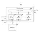
- 1 is a block diagram showing a configuration example of an integrated circuit according to a first embodiment of the present technology
- 1 is a block diagram showing a configuration example of an analog-to-digital converter according to a first embodiment of the present technology
- 1 is a block diagram showing a configuration example of a stochastic ADC according to a first embodiment of the present technology
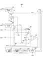
- 3A and 3B are a circuit diagram and a timing chart illustrating a configuration example of a multi-phase clock generating unit according to the first embodiment of the present technology
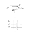
- 1A and 1B are a circuit diagram and a timing chart illustrating a configuration example of an end pulse generating unit according to a first embodiment of the present technology
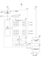
- 3 is a block diagram showing a configuration example of a correction unit according to the first embodiment of the present technology
- FIG. 4 is a diagram showing an example of a waveform of an internal signal indicated by waveform data in the first embodiment of the present technology
- FIG. 1 is a graph showing an example of PVT (Process, Voltage, and Temperature) variation of a waveform in a first embodiment of the present technology.
- 10A to 10C are diagrams for explaining a tendency of an evaluation value in the first embodiment of the present technology;
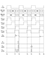
- 4 is a timing chart showing an example of an operation of the analog-to-digital converter up to sampling of a sampling clock signal according to the first embodiment of the present technology.
- 4 is a timing chart showing an example of an operation of the analog-to-digital converter when sampling an internal signal according to the first embodiment of the present technology.
- FIG. 1A to 1C are diagrams for explaining a method for measuring a phase interval according to a first embodiment of the present technology
- 11A to 11C are diagrams for explaining another method for measuring a phase interval in the first embodiment of the present technology.
- 4 is a flowchart showing an example of an operation of the integrated circuit according to the first embodiment of the present technology.
- 11 is a flowchart illustrating an example of a phase interval correction process according to the first embodiment of the present technology.
- FIG. 1 is a block diagram showing a configuration example of a stochastic ADC in a comparative example.
- FIG. 13 is a block diagram showing a configuration example of a correction unit in a comparative example.
- FIG. 13 is a diagram for explaining the influence of fluctuations in phase intervals.
- FIG. 13 is a timing chart showing an example of a foreground process according to the second embodiment of the present technology; 13 is a timing chart showing an example of an operation after a foreground process in the second embodiment of the present technology.
- 13 is a flowchart showing an example of an operation of the integrated circuit according to the second embodiment of the present technology.
- 13 is a flowchart illustrating an example of a phase interval correction process according to the second embodiment of the present technology.
- FIG. 13 is a block diagram showing a configuration example of an analog-to-digital converter according to a third embodiment of the present technology.
- FIG. 13 is a circuit diagram showing a configuration example of a first stage according to a third embodiment of the present technology.
- FIG. 13 is a block diagram showing a configuration example of an integrated circuit according to a fourth embodiment of the present technology.
- FIG. 13 is a block diagram showing a configuration example of a stochastic ADC according to a fourth embodiment of the present technology.
- FIG. 13 is a block diagram showing a configuration example of a correction unit according to a fourth embodiment of the present technology.
- FIG. 13 is a diagram illustrating an example of a waveform of a pulse signal indicated by waveform data in a fourth embodiment of the present technology.
- FIG. 13 is a circuit diagram showing a configuration example of a multi-phase clock generating unit according to a fifth embodiment of the present technology. 13 is a timing chart showing an example of an operation of a multi-phase clock generating unit according to the fifth embodiment of the present technology;
- First embodiment (example of correcting phase intervals of multi-phase clocks) 2.
- Second embodiment (example of correcting phase intervals of multi-phase clocks in foreground processing) 3.
- Third embodiment (example of correcting the settling time of an internal signal between stages outputting 1.5 bits and the phase interval of a multi-phase clock) 4.
- Fourth embodiment (example of correcting pulse width of pulse signal and phase interval of multi-phase clock) 5.
- Fifth embodiment example of correcting phase intervals of multi-phase clocks by controlling variable current sources and variable capacitance circuits)
- First embodiment [Example of integrated circuit configuration] 1 is a block diagram showing an example of a configuration of an integrated circuit 100 according to an embodiment of the present technology.
- the integrated circuit 100 is a circuit having an AD (Analog to Digital) conversion function, and is arranged in various devices and equipment such as wireless communication devices and information processing devices.
- the integrated circuit 100 includes an analog signal generating section 110, a sampling clock generating section 120, an analog-to-digital converter 200, a control section 130, and a digital signal processing section 140.
- the analog signal generating section 110 generates an analog signal V IN .
- the analog signal generating section 110 supplies the analog signal V IN to the analog-to-digital converter 200 via a signal line 119.
- a voltage signal is used as the analog signal V IN .
- the sampling clock generating unit 120 generates the sampling clock signal Fs. This sampling clock generating unit 120 supplies the sampling clock signal Fs to the analog-to-digital converter 200 and the control unit 130 via a signal line 129.
- the analog-to-digital converter 200 converts the analog signal V IN into a digital signal D out in synchronization with a sampling clock signal Fs having a predetermined frequency.
- the analog-to-digital converter 200 supplies the digital signal D out to the digital signal processing unit 140 via a signal line 209.
- the control unit 130 controls the operation of the analog-to-digital converter 200.
- the digital signal processing unit 140 performs various signal processing operations on the digital signal D out .
- analog signal generating unit 110 the sampling clock generating unit 120, the analog-to-digital converter 200, the control unit 130, and a part of the digital signal processing unit 140 (such as the analog signal generating unit 110) can also be arranged outside the integrated circuit 100.
- FIG. 2 is a block diagram showing an example of a configuration of an analog-to-digital converter 200 according to the first embodiment of the present technology.
- the analog-to-digital converter 200 includes a pipelined ADC 210 and a stochastic ADC 300.
- the pipelined ADC 210 converts an analog signal V IN into a digital signal D out in synchronization with a sampling clock signal Fs.
- the pipelined ADC 210 includes a first stage 220, a second stage 230, an adder 240, and a state control section 250.
- the first stage 220 includes a first ADC 221, a DAC (Digital to Analog Converter) 222, a subtractor 223, a shift calculator 224, and an amplifier 225.
- the second stage 230 includes a second ADC 231.
- the first ADC 221 converts the analog signal V IN into a digital signal D 1.
- a SAR ADC Successessive Approximation Register Analog to Digital Converter
- the digital signal D 1 indicates the most significant bits of the digital signal D out .
- the first ADC 221 supplies the digital signal D 1 to the DAC 222 and the shift calculator 224.
- the shift calculator 224 performs a shift operation on the digital signal D 1 to obtain a value equivalent to the most significant bit of D out , and supplies this value to the adder 240 .
- the DAC 222 converts the digital signal D 1 into an analog signal and supplies it to the subtractor 223 .
- the subtractor 223 supplies the difference between the analog signal V IN and the analog signal from the DAC 222 as an analog signal V RI to the amplifier 225.
- This analog signal V RI is a signal corresponding to the quantization error of the digital signal D1 .
- the amplifier 225 amplifies the analog signal V_RI and supplies it to the second ADC 231 and the stochastic ADC 300 as an internal signal V_RO .
- the second ADC 231 converts the internal signal VRO into a digital signal D2 .
- a SAR ADC is used as the second ADC 231.
- the digital signal D2 indicates the lower bits of the digital signal Dout .
- the second ADC 231 supplies the digital signal D2 to the adder 240 and the stochastic ADC 300.
- the adder 240 adds the digital signal D 1 multiplied by a power of 2 by the shift calculator 224 and D 2 , and supplies the result to the digital signal processor 140 as a digital signal D out .
- the state control unit 250 controls the operation of the first ADC 221 and the second ADC 231 in synchronization with the sampling clock signal Fs.
- the state control unit 250 also supplies a portion of the control signal for controlling the first ADC 221 to the stochastic ADC 300.
- the stochastic ADC 300 corrects the settling time of the internal signal VRO .
- the stochastic ADC 300 generates a control signal Cset based on the internal signal VRO and supplies it to the amplifier 225.
- the control signal Cset is, for example, a signal that controls the bias current of a transistor in the amplifier 225.
- the settling time is corrected by controlling the bias current.
- the number of stages in the pipelined ADC 210 is two, it may be three or more. When there are three or more stages, there will be two or more amplifiers between the stages. In this case, a stochastic ADC 300 can be placed for each amplifier, but the circuit size of the analog-to-digital converter 200 increases as the number of amplifiers increases. For this reason, from the perspective of cost-effectiveness, it is preferable to preferentially provide the stochastic ADC 300 in the amplifiers of the higher bits and reduce the number of stochastic ADCs 300 in the amplifiers of the lower bits.
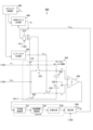
- [Configuration example of stochastic ADC] 3 is a block diagram showing an example of a configuration of a stochastic ADC 300 according to the first embodiment of the present technology.
- the stochastic ADC 300 includes a multi-phase clock generating unit 400, a demultiplexer 310, an end pulse generating unit 320, a sample-and-hold circuit 330, a comparator 340, an average value calculating unit 351, an error function calculating unit 352, a normalizing unit 353, and a correcting unit 500.
- the sample-and-hold circuit 330 includes sample switches 331, 332, 333, and 334, and capacitances 335 and 336.
- the multi-phase clock generating unit 400 generates a clock pulse ⁇ n whose phase is controlled to one of a plurality of phases, and supplies the clock pulse ⁇ n to the demultiplexer 310.
- n is an integer from 1 to N
- N is an integer of 2 or more indicating the number of phases.
- the phase of ⁇ n corresponds to the n-th phase among the N phases.
- the multi-phase clock generating unit 400 receives a control signal ST1 hold' from the pipelined ADC 210 and a control signal C delay from the correction unit 500.
- the control signal ST1 hold' is a control pulse that advances the hold period of the first stage 220.
- the multi-phase clock generating unit 400 generates a clock pulse ⁇ n based on the control signal ST1 hold' .
- the delay time in the multi-phase clock generating unit 400 is controlled by the control signal C delay . Since the control signal ST1 hold' is a signal generated in synchronization with the sampling clock signal Fs, the clock pulse ⁇ n is also a signal synchronized with the sampling clock signal Fs.
- the demultiplexer 310 switches the output destination of the clock pulse ⁇ n in accordance with a control signal SELc from the control unit 130.
- the clock pulse ⁇ n is output to the sample switch 333 in response to the control signal SELc.
- the clock pulse ⁇ n is output to the sample switches 331 and 332 in response to the control signal SELc.
- the clock pulse output to the sample switches 331 and 332 will be referred to as ⁇ cal_n in order to distinguish it from the clock pulse output to the sample switch 334.
- the end pulse generating section 320 generates an end pulse ⁇ end based on a control signal ST1 hold' from the pipelined ADC 210. This end pulse ⁇ end indicates the timing immediately before the end of the sampling period of the second ADC 231. The end pulse generating section 320 supplies the end pulse ⁇ end to the sample switch 334.
- the sample switch 331 synchronizes with the clock pulse ⁇ cal_n and holds the voltage of the sampling clock signal Fs in the capacitor 335 as a positive voltage V+.
- the sample switch 332 synchronizes with the clock pulse ⁇ cal_n and holds a predetermined threshold voltage as a negative voltage V- in the capacitor 336.
- the threshold voltage is a voltage for determining whether or not the sampling clock signal Fs is at a high level.
- the high level of the sampling clock signal Fs is set to VDD, and VDD/2 is used as the threshold voltage.
- the sample switch 333 synchronizes with the clock pulse ⁇ n and holds the voltage of the internal signal V RO as a positive voltage V+ in the capacitor 335.
- the sample switch 334 synchronizes with the end pulse ⁇ end and holds the voltage of the internal signal V RO as a negative voltage V- in the capacitor 336.
- the sample-and-hold circuit 330 holds the voltage of the internal signal VRO as a positive voltage V+ and a negative voltage V- in synchronization with the clock pulse ⁇ n and the end pulse ⁇ end during the sample period of the second ADC 231. In addition, outside the sample period, the sample-and-hold circuit 330 holds the voltage of the sampling clock signal Fs and a threshold voltage (such as VDD/2) as a positive voltage V+ and a negative voltage V- in synchronization with the clock pulse ⁇ cal_n .
- a threshold voltage such as VDD/2
- Comparator 340 compares the positive voltage V+ and the negative voltage V-, and outputs a bit indicating the comparison result to average value calculation unit 351.
- the average value calculation unit 351 calculates the average value E of a predetermined number of bits output from the comparator 340. This average value E is calculated for each phase. If there are N phases, N average values E are calculated.
- the distribution of the analog internal signal V RO is a normal distribution due to sampling noise (in other words, kTC noise) and input-referred noise in the comparator 340. Therefore, the comparison result of the comparator 340 for the same digital signal D 2 is not constant, and the bit of the comparison result changes to "0" or "1” every time the comparison is made.
- the cumulative probability density ⁇ (V RO ) at which the comparator 340 outputs "0” changes depending on the relative positional relationship between the internal signal V RO and the threshold voltage in the comparator 340.
- the sample-and-hold circuit 330 and the comparator 340 perform sampling and comparison multiple times, and the average value calculation unit 351 calculates the average value E of these, so that the cumulative probability density ⁇ (V RO ) can be estimated.
- the error function calculation unit 352 can estimate the voltage of the internal signal VRO by calculating Equation 4. However, this is a normalized equation when the input dynamic range is [-1, 1] and ⁇ of the normal distribution is 1. Therefore, when the input dynamic range is defined by the reference voltage VREF as [ -VREF , VREF ], the voltage of the internal signal VRO can be found for any ⁇ by the following equation.
- the voltage of the internal signal VRO can be estimated by any one of Equation 4, Equation 5, and Equation 6.
- Equation 5 the average value calculation unit 351 calculates the average value E
- the error function calculation unit 352 and the normalization unit 353 calculate the internal signal VRO by Equation 5 and supply it to the correction unit 500.
- the average value calculation section 351 calculates the average value E
- the error function calculation section 352 calculates the internal signal VRO using Equation 4, and supplies the signal to the correction section 500.
- the normalization section 353 can be omitted.
- the average value calculation section 351 calculates the internal signal V RO using Equation 6 and supplies the signal to the correction section 500.
- the error function calculation section 352 and the normalization section 353 can be omitted.
- VRO which is the output of the interstage amplifier 225
- VRI which is the input voltage of the amplifier 225.
- the stochastic ADC 300 cannot directly know VRI , D2 , which is the output of the second ADC 231 of the second stage 230, is obtained by AD conversion of VRI .
- the average value calculator 351 finds an average value for each value of the digital signal D2 .
- M ⁇ N average values E are calculated.
- the average value calculator 351 holds bits indicating the comparison results for each combination of phase and digital signal D2 , and calculates the average value E when the number of bits corresponding to a certain combination reaches a certain number.
- the correction unit 500 corrects the settling time and the phase interval based on waveform data in which the calculation results of Equation 4, Equation 5, or Equation 6 are arranged.
- the correction unit 500 generates a control signal C set for correcting the settling time and supplies it to the amplifier 225.
- the correction unit 500 also generates a control signal C delay for correcting the phase interval and supplies it to the multi-phase clock generation unit 400.
- Example of the configuration of the multi-phase clock generation unit] 4 is a circuit diagram and a timing chart showing a configuration example of the multi-phase clock generating unit 400 according to the first embodiment of the present technology.
- the multi-phase clock generating unit 400 includes, for example, inverters 411 and 412, a fixed delay unit 413, a NOR (negative OR) gate 414, and a variable capacitance circuit 420.
- the inverter 411 inverts the control signal ST1 hold' and supplies it as a signal A to the inverter 412 and the NOR gate 414.
- the inverter 412 inverts the signal A from the inverter 411 and supplies it to the fixed delay section 413.
- the fixed delay section 413 delays the signal from the inverter 412 for a fixed delay time and supplies it to the NOR gate 414 as a signal B.
- the NOR gate 414 supplies the NOR of the signals A and B to the demultiplexer 310 as a clock pulse ⁇ n .
- the variable capacitance circuit 420 includes a plurality of connection switches 421 and the same number of capacitances 422 as the number of the switches.
- the connection switches 421 connect the connection node of the inverters 412 and 412 to one end of the corresponding capacitance 422 in accordance with a control signal C delay from the correction unit 500. The other end of the capacitance 422 is grounded.
- signal A which is an inverted and delayed version of the control signal ST1 hold'
- signal B which is an inverted and delayed version of signal A
- a clock pulse ⁇ n is generated by the NOR of signals A and B.
- the pulse width from timing T1 to T2 corresponds to the delay time in the inverter 412 and the fixed delay unit 414.
- the correction unit 500 can change the composite capacitance of the variable capacitance circuit 420 by changing the number of capacitances 422 connected in parallel by the control signal C delay .
- the delay time of the clock pulse ⁇ n with respect to the control signal ST1 hold' can be controlled.
- the phase of the clock pulse ⁇ n can be controlled and the phase interval (time resolution) can be corrected.
- the delay time is controlled to ⁇ t ⁇ n.
- Example of the configuration of the end pulse generating unit] 5 is a circuit diagram and a timing chart showing a configuration example of the end pulse generating unit 320 according to the first embodiment of the present technology.
- the end pulse generating unit 320 includes a fixed delay unit 321 and an AND (logical product) gate 322.
- the fixed delay unit 321 delays the control signal ST1 hold' for a fixed delay time and supplies the delayed signal to the AND gate 322 as a signal C.
- the AND gate 322 outputs the logical product of the control signal ST1 hold' and the signal C as an end pulse ⁇ end to the sample-and-hold circuit 330.
- a delayed signal C of the control signal ST1 hold' falls at timing T1.
- An end pulse ⁇ end is generated by ANDing the control signal ST1 hold' and the signal C.
- the time from timing T0 to T1 corresponds to the delay time of the fixed delay unit 321. The delay times are adjusted so that the period when the end pulse ⁇ end is at a high level does not overlap with the period when the clock pulse ⁇ cal_n is at a high level.
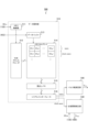
- the correction unit 500 includes a data holding unit 510, a settling time correction unit 520, and a phase interval correction unit 530.
- the data holding unit 510 includes a memory control unit 511, a row and column address decoder 512, a data buffer 513, a memory cell array 514, a read bus 515, and a serial interface 516.
- a memory such as a static random access memory (SRAM) is used.
- the memory control unit 511 receives the digital signal D2 from the pipelined ADC 210 and the control signal SELc from the control unit 130.
- the control signal SELc is a signal for switching the output destination of the demultiplexer 310 depending on whether or not it is within the sampling period of the second ADC 231, as described above.
- an address is assigned for each possible value of the digital signal D2 .
- waveform data wave[m] (m is an integer from 1 to M) is held in each of the M addresses.
- This waveform data wave indicates the waveform of the internal signal VRO and includes N pieces of data D(t n ).
- the data D(t n ) is the calculation result of Equation 4, Equation 5, or Equation 6 for a group of comparison results of the nth phase out of the N pieces (in other words, the height of the waveform).
- the waveform data clock_wave is held in an address separate from the M addresses for the waveform data wave[m]. Each of these M+1 addresses includes a row address and a column address.
- the waveform data clock_wave indicates the waveform of the sampling clock signal Fs and includes N pieces of data D(t n ).
- the data D(t n ) is the calculation result (waveform height) of the equation 4 or the like for the group of comparison results of the nth phase.
- the memory control unit 511 supplies an address (row address and column address) corresponding to the value of the digital signal D2 to the row/column address decoder 512.
- the memory control unit 511 supplies an address for holding the waveform data clock_wave to the row/column address decoder 512.
- the row and column address decoder 512 decodes the address from the memory control unit 511. Based on the decoded result, the row and column address decoder 512 controls the voltage of the word lines and bit lines of the memory cell array 514, and stores the waveform data in the data buffer 513 at the corresponding address.
- the data buffer 513 stores the waveform data wave[m] and the waveform data clock_wave.
- the read bus 515 sequentially reads out M pieces of waveform data wave[m] and the waveform data clock_wave.
- the serial interface 516 performs parallel-serial conversion on the read data and supplies it to the settling time correction unit 520 and the phase interval correction unit 530.
- the waveform data wave[m] is supplied to the settling time correction unit 520, and the waveform data clock_wave is supplied to the phase interval correction unit 530.
- the settling time correction section 520 evaluates and corrects the settling time of the internal signal V_RO based on the waveform data wave[m].
- the settling time correction section 520 generates a control signal C_set and supplies it to the pipelined ADC 210.
- the waveform of the internal signal VRO becomes a settling waveform and varies with time. Therefore, by calculating the average value of the comparison result of the comparator 340 using the above-mentioned formula 4 or the like, the voltage of the internal signal VRO for each phase can be estimated. As a result, the entire time-varying settling waveform can be estimated.
- the calculation result for each phase corresponds to the data D(t n ) in the waveform data wave[m]. Normally, if the phase interval (time resolution) is not sufficiently small compared to the frequency of the sampling clock signal Fs, a waveform cannot be obtained, so a multi-phase clock must be prepared.
- the phase interval correction unit 530 corrects the intervals between N phases based on the waveform data clock_wave.
- a control signal SELp indicating which of the N phases to select is input to this phase interval correction unit 530 from the control unit 130.
- the phase interval correction unit 530 measures the phase interval based on the waveform data clock_wave.
- the phase interval of the multi-phase clock is constant. However, if the multi-phase clock generation unit 400 delays the signal using resistance or capacitance, the phase interval may change due to PVT variations. If the phase interval is too large, the number of sample points will be reduced relative to the sample period of the second ADC 231, and the settling time correction unit 520 will not be able to correctly evaluate the settling time. Conversely, if the phase interval is too small, the measurement dynamic range will be insufficient relative to the sample period, and the latter half of the settling waveform will not be able to be correctly evaluated.
- the phase interval correction unit 530 If the appropriate value of the phase interval is ⁇ t and the phase indicated by the control signal SELp is the nth phase, the phase interval correction unit 530 generates a control signal C delay for setting the delay time to ⁇ t ⁇ n, and supplies the control signal C delay to the multi-phase clock generation unit 400. Through this control, the phase interval is corrected to an appropriate value.
- the correction unit 500 generates M pieces of waveform data wave[m], the settling time can be evaluated even with one piece of waveform data wave[m]. Therefore, although there is a trade-off with the convergence speed of the correction, the number of these waveform data can be reduced, thereby reducing the hardware implementation area and power consumption.
- FIG. 7 is a diagram showing an example of the waveform of the internal signal VRO shown in the waveform data according to the first embodiment of the present technology.
- the vertical axis indicates the voltage of the internal signal VRO
- the horizontal axis indicates time.
- the internal signal VRO varies over time when sampled.
- the average value calculation unit 351 etc. calculates VRO for each timing using Equation 4 etc.
- the memory cell array 514 holds waveform data in which the calculation results D( t1 ) to D( tN ) are arranged.
- FIG. 8 is a graph showing an example of PVT variation of a waveform in the first embodiment of the present technology.
- the vertical axis indicates the voltage of the internal signal VRO
- the horizontal axis indicates time.
- the dashed-dotted curve indicates a waveform under the conditions of a process of SS, a power supply voltage of 0.76 volts (V), and a temperature of 105° C.
- SS indicates that both p-channel and n-channel are Slow device models.
- the solid curve indicates a waveform under the conditions of a process of TT, a power supply voltage of 0.80 volts (V), and a temperature of 25° C. TT indicates that both p-channel and n-channel are Typical device models.
- the dotted curve indicates a waveform under the conditions of a process of FF, a power supply voltage of 0.84 volts (V), and a temperature of ⁇ 20° C.
- FF indicates that both p-channel and n-channel are Fast device models.
- the waveform of the internal signal VRO changes depending on the PVT conditions.
- N points are sampled within a sample period, and N pieces of data D( tn ) are generated. All of these pieces of data are designated as D[1:N].
- a group of data in the latter half of the settling time is designated as data D[x:N], where x is an integer equal to or greater than 2 and less than N.
- the settling time correction unit 520 calculates an evaluation value, for example, by the following formula:
- Stdev( ) represents a function that returns the standard deviation.
- FIG. 9 is a diagram for explaining the tendency of the evaluation value in the first embodiment of the present technology.
- the power supply voltage is 0.76 volts (V)
- the temperature is 105°C, for example
- the waveform will be in an "Unstable, Under-Damped" state.
- the numerator of Equation 7 will be relatively large, and the denominator will be medium.
- the evaluation value will be a medium value.
- the power supply voltage is 0.80 volts (V)
- the temperature is 25°C, for example, the waveform is in a "Criticaly-Damped" state.
- the numerator of Equation 7 becomes relatively large and the denominator becomes extremely small. As a result, the evaluation value becomes relatively large.
- the waveform will be in an "over-damped" state.
- both the numerator and denominator of Equation 7 will be in the middle range. As a result, the evaluation value will be relatively small.
- the settling time correction unit 520 corrects the settling time based on the evaluation value.
- the settling time correction unit 520 calculates, for example, statistics (average or sum) of the M evaluation values and corrects the settling time based on the statistics.
- FIG. 10 is a timing chart showing an example of the operation of the analog-to-digital converter 200 up to the sampling of the sampling clock signal Fs in the first embodiment of the present technology.
- the first ADC 221 and the second ADC 231 operate in synchronization with the sampling clock signal Fs. Within the period of the sampling clock signal Fs from T0 to T2, the first ADC 221 samples a signal and performs AD conversion in the period from timing T0 to T1 in accordance with the control signals ST1_samp and ST1_comv . Within that period, the second ADC 231 performs AD conversion.
- the first ADC 221 holds the signal in accordance with the control signal ST1_hold , and during this period, the second ADC 231 samples the signal.
- the internal signal V_RO fluctuates during this period.
- the stochastic ADC 300 samples the voltage of the internal signal V_RO in synchronization with the clock pulse ⁇ _n and the end pulse ⁇ _end during the sample period of the second ADC 231, and compares the voltages.
- the period from timing T1 to t_end corresponds approximately to the sample period.
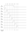
- the stochastic ADC 300 samples the voltage of the sampling clock signal Fs and VDD/2 in synchronization with the clock pulse ⁇ cal_n and compares them to measure the phase interval.
- the period from the rising timing T4 of the sampling clock signal Fs until a certain time has elapsed corresponds to the measurement period of the phase interval.
- the phase of the clock pulse ⁇ cal_n is controlled to the first phase out of the N phases.
- the phase of the clock pulse ⁇ cal_n is controlled to the second phase. Thereafter, the phase is switched for each measurement.
- FIG. 11 is a timing chart showing an example of the operation of the analog-to-digital converter when sampling the internal signal VRO in the first embodiment of the present technology.
- the settling time is corrected after timing T7 after sampling of the sampling clock signal Fs.
- the stochastic ADC 300 samples the voltage of the internal signal VRO in synchronization with the clock pulse ⁇ 1 and the end pulse ⁇ end within the sample period from timing T7.
- the stochastic ADC 300 samples the voltage of the internal signal VRO in synchronization with the clock pulse ⁇ 2 and the end pulse ⁇ end within the sample period from timing T9.
- the stochastic ADC 300 samples the voltage of the internal signal VRO in synchronization with the clock pulse ⁇ 3 and the end pulse ⁇ end within the sample period from timing T11. After that, the phase of the clock pulse ⁇ n is switched every time a period of the sampling clock signal Fs elapses.
- the stochastic ADC 300 performs one comparison for correcting the phase interval every time it performs N comparisons for correcting the settling time. This allows the stochastic ADC 300 to correct the phase interval in parallel in the background of the settling time correction process.
- this type of processing will be referred to as "background processing.”
- phase interval correction unit 530 corrects the phase interval from the waveform data clock_wave.
- FIG. 12 is a diagram for explaining a method for measuring a phase interval in the first embodiment of the present technology. It is assumed that there are eight phases in total, and clock pulses ⁇ cal_1 to ⁇ cal_8 are generated in order. The timings of their falling edges (in other words, phases) are t 1 to t 8 .
- the phase interval correction unit 530 can estimate the phase interval ⁇ t (time resolution). Based on this estimation result, the phase interval correction unit 530 can adjust the delay time of the multi-phase clock generation unit 400 to an appropriate value. For example, when T H /4 is the ideal value of the phase interval, the current phase interval is too small, so the phase interval correction unit 530 applies feedback to increase the phase interval.
- FIG 13 shows another example of measuring the phase intervals in the period of the sampling clock signal F S.
- clock pulses ⁇ cal_1 to ⁇ cal_8 are arranged in the same cycle to make the timing relationship easier to understand.
- the phase interval correction unit 530 can estimate the phase interval ⁇ t (time resolution).
- FIG. 14 is a flowchart showing an example of the operation of the integrated circuit 100 in the first embodiment of the present technology. This operation is started, for example, when the integrated circuit 100 is powered on.
- the control unit 130 in the integrated circuit 100 initializes variables i and j to "1" or the like (step S901).
- the analog-to-digital converter 200 samples the internal signal VRO at timings t i and t end (step S902), and compares these voltages with the stochastic ADC 300 (step S903).
- the analog-digital converter 200 holds the comparison results and performs various post-processing. For example, the analog-digital converter 200 performs a calculation such as Equation 4 on a certain number of comparison results and generates waveform data in which the calculation results for each phase are arranged. The analog-digital converter 200 then corrects the settling time of the internal signal VRO based on the waveform data (step S904).
- the control unit 130 determines whether the variable i is N (step S905). If the variable i is not N (step S905: No), the control unit 130 increments the variable i (step S907) and repeats steps S902 and onward.
- step S905 if the variable i is N (step S905: Yes), the control unit 130 initializes the variable i (step S906) and performs a phase interval correction process (step S910). After step S910, the control unit 130 repeats steps S902 and onward.
- the analog-to-digital converter 200 samples the voltage of the sampling clock signal Fs and VDD/2 at timing tj (step S911), and compares these voltages with the stochastic ADC 300 (step S912).
- the analog-digital converter 200 holds the comparison results and performs various post-processing. For example, the analog-digital converter 200 performs calculations such as Equation 4 on a certain number of comparison results, and generates waveform data in which the calculation results for each phase are arranged. The analog-digital converter 200 then corrects the phase interval based on the waveform data (step S913).
- the control unit 130 determines whether the variable j is N (step S914). If the variable j is not N (step S914: No), the control unit 130 increments the variable j (step S917) and ends the phase interval correction process.
- step S914 if the variable j is N (step S914: Yes), the control unit 130 initializes the variable j (step S916) and ends the phase interval correction process.
- FIG. 16 is a block diagram showing an example of a configuration of a stochastic ADC 300 in a comparative example.
- the demultiplexer 310 and the sample switches 331 and 332 are omitted. Therefore, the sampling clock signals Fs and VDD/2 are not sampled.
- FIG. 17 is a block diagram showing an example of the configuration of the correction unit 500 in a comparative example.
- the phase interval correction unit 530 is omitted.
- the waveform data clock_wave is not stored in the memory cell array 514.
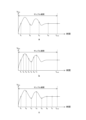
- a shows the waveform of the internal signal VRO when the phase interval is larger than the ideal value.
- b shows the waveform of the internal signal VRO when the phase interval is smaller than the ideal value.
- c shows the waveform of the internal signal VRO when the phase interval is the ideal value.
- the vertical axis of a, b, and c shows the internal signal VRO
- the horizontal axis shows time.
- the phase interval may vary due to PVT variations. If the phase interval is larger than the ideal value, as shown in a in the figure, there are insufficient points to sample within the sample period up to t end , and the settling time cannot be evaluated correctly. Conversely, if the phase interval is smaller than the ideal value, as shown in b in the figure, the measurement dynamic range is insufficient for the sample period, and the latter half of the settling waveform cannot be evaluated correctly. These variations in phase interval reduce the AD conversion accuracy of the stochastic ADC 300, and the settling time cannot be corrected to an appropriate value.
- the phase interval correction unit 530 corrects the phase interval to an ideal value as shown in c in the figure, thereby improving the AD conversion accuracy of the stochastic ADC 300.
- Using a DLL as the multi-phase clock generation unit 400 allows for the generation of highly accurate multi-phase clocks, but is not preferred due to increased power consumption and circuit area.
- the phase interval correction unit 530 is a digital circuit.
- the demultiplexer 310 and sample switches 331 and 332 can be realized using transistor groups, so the increase in power consumption and circuit size is suppressed compared to a DLL.
- the phase interval correction unit 530 corrects the phase intervals of the multi-phase clocks, thereby improving the AD conversion accuracy of the stochastic ADC 300.
- the correction unit 500 corrects the phase interval by background processing. This allows the correction unit 500 to follow the fluctuation of the phase interval due to PVT variations, but it takes time for the correction to converge because the comparison for correcting the phase interval is performed between comparison operations for correcting the settling time.
- the analog-to-digital converter 200 in the second embodiment differs from the first embodiment in that the phase interval is corrected before the correction process for the settling time.
- 19 is a timing chart showing an example of foreground processing in the second embodiment of the present technology.
- the analog-to-digital converter 200 samples and compares the sampling clock signal Fs and VDD/2 in synchronization with the clock pulse ⁇ cal_n .
- the phase of the clock pulse ⁇ cal_n is switched for each cycle of the sampling clock signal Fs.
- phase interval correction unit 530 in the analog-to-digital converter 200 generates waveform data clock_wave and corrects the phase interval based on that data. This process of correcting the phase interval before the settling time correction process is called “foreground processing.” This foreground processing ends at timing T6.
- FIG. 20 is a timing chart showing an example of the operation after foreground processing in the second embodiment of the present technology. After timing T6, the settling time and phase interval are corrected by a sequence similar to that of the first embodiment.
- FIG. 21 is a flowchart showing an example of the operation of the integrated circuit 100 in the second embodiment of the present technology.
- the operation of the integrated circuit 100 in this second embodiment differs from the first embodiment in that a phase interval correction process (step S920) is further executed between steps S901 and S902.
- This step S920 corresponds to the foreground process described above.
- step S920 is a flowchart showing an example of a phase interval correction process (step S920) according to the second embodiment of the present technology.
- the analog-to-digital converter 200 samples the voltage of the sampling clock signal Fs and VDD/2 at timing tj (step S921), and compares these voltages with the stochastic ADC 300 (step S922).
- the analog-digital converter 200 holds the comparison results and performs various post-processing. For example, the analog-digital converter 200 performs calculations such as Equation 4 on a certain number of comparison results, and generates waveform data in which the calculation results for each phase are arranged. The analog-digital converter 200 then corrects the phase interval based on the waveform data (step S923).
- the control unit 130 determines whether the variable j is N (step S924). If the variable j is not N (step S924: No), the control unit 130 increments the variable j (step S926) and repeats steps S921 and onward.
- step S924 if the variable j is N (step S924: Yes), the control unit 130 initializes the variable j (step S925) and ends the phase interval correction process.
- the number of comparisons for each phase is set to one.
- the phase interval correction unit 530 corrects the phase interval by foreground processing, so the time it takes for the phase interval correction to converge can be shortened compared to the first embodiment.
- an ADC such as a SAR ADC is arranged for each stage, but an ADC that outputs two bits representing one of three values can also be arranged for each stage.
- the analog-to-digital converter 200 in this third embodiment differs from the first embodiment in that the ADC for each stage outputs two bits representing one of three values.
- FIG. 23 is a block diagram showing an example of the configuration of an analog-to-digital converter 200 in a third embodiment of the present technology.
- the pipelined ADC 210 in this third embodiment differs from the first embodiment in that it includes S stages (S is an integer equal to or greater than 2), such as a first stage 220 and a second stage 230, and a digital value adder 260.
- Each stage supplies two bits (so-called 1.5 bits) representing one of three values to the digital value adder 260.
- the digital value adder 260 adds them together and outputs the result as D out .
- the stochastic ADC 300 can be placed for each amplifier, but the circuit size of the analog-to-digital converter 200 increases as the number of amplifiers increases. For this reason, from a cost-effectiveness perspective, it is preferable to provide the stochastic ADC 300 preferentially to the amplifiers of the higher bits and to reduce the number of stochastic ADCs 300 for the amplifiers of the lower bits. In the figure, the stochastic ADC 300 is connected only to the interstage amplifiers of the first stage 220 and the second stage 230.
- the second stage 24 is a circuit diagram showing a configuration example of the first stage 220 in the third embodiment of the present technology.
- the first stage 220 includes a first ADC 221, a DAC 222, a subtractor 223, and an amplifier 225.
- the amplifier 225 amplifies V RI by 2 times and outputs the amplified signal.
- DAC 222, subtractor 223, and amplifier 225 are realized, for example, by sample switches 271, 272, and 273, capacitors 274 and 275, short-circuit switches 276 and 277, and operational amplifier 278.
- the circuit configuration of each stage after second stage 230 is the same as that of first stage 220.
- the sample switch 271 in accordance with the clock pulse ⁇ 1 , opens and closes a path between an input node to which an analog signal VIN is input and one end of a capacitor 274.
- the sample switch 272, in accordance with the clock pulse ⁇ 1 opens and closes a path between the input node and one end of a capacitor 275.
- the sample switch 273 opens and closes a path between a node of a predetermined internal voltage V DAC and one end of a capacitor 275 in accordance with a clock pulse ⁇ 2.
- the other ends of the capacitors 274 and 275 are commonly connected to an inverting input terminal ( ⁇ ) of an operational amplifier 278.
- the non-inverting input terminal (+) of the operational amplifier 278 is grounded.
- the internal signal V RO is output from the operational amplifier 278 to the second stage 230 and the stochastic ADC 300.
- the short-circuit switch 277 opens and closes the path between the connection node of the sample switch 271 and the capacitor 274 and the output terminal of the operational amplifier 278 in accordance with the clock pulse ⁇ 2 .
- the short-circuit switch 276 opens and closes the path between the non-inverting input terminal (+) and the inverting input terminal (-) of the operational amplifier 278 in accordance with the clock pulse ⁇ 1a .
- the second embodiment can be applied to the third embodiment.
- the stochastic ADC 300 is connected to the interstage op-amp 278 that outputs 1.5 bits, so the settling time of the output can be corrected.
- stochastic ADC 300 corrects the settling time of internal signal VRO from the amplifier in pipelined ADC 210, but is not limited to this configuration.
- Stochastic ADC 300 in this fourth embodiment differs from the first embodiment in that it corrects the pulse width of a pulse signal.
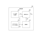
- FIG. 25 is a block diagram showing an example of the configuration of an integrated circuit 100 according to a fourth embodiment of the present technology.
- the integrated circuit 100 according to the fourth embodiment includes a pulse signal generating unit 150, a sampling clock generating unit 120, a stochastic ADC 300, and a control unit 130.
- the stochastic ADC 300 is an example of an analog-to-digital converter as described in the claims.
- the pulse signal generating unit 150 generates a pulse signal PLS.
- This pulse signal PLS is used to drive a driver (not shown) and is also input to the stochastic ADC 300.
- the sampling clock generating unit 120 supplies the sampling clock signal Fs to the stochastic ADC 300 and the control unit 130.
- the control unit 130 controls the operation of the stochastic ADC 300.
- the stochastic ADC 300 measures the width of the pulse signal PLS and outputs a digital signal D PLS indicating the measured value.
- the digital signal D PLS is used for correcting the pulse width, etc.
- FIG. 26 is a block diagram showing an example configuration of a stochastic ADC 300 according to a fourth embodiment of the present technology.
- the stochastic ADC 300 according to the fourth embodiment further includes a timing control unit 360.
- the timing control unit 360 generates a control signal synchronized with the sampling clock signal Fs and supplies it to the multi-phase clock generation unit 400 and the end pulse generation unit 320.
- the noise in the pulse signal PLS is low, all or part of the average value calculation unit 351, the error function calculation unit 352, and the normalization unit 353 can be eliminated.
- FIG. 27 is a block diagram showing an example of the configuration of a correction unit 500 in a fourth embodiment of the present technology.
- the correction unit 500 in this fourth embodiment differs from the first embodiment in that it includes a pulse width measurement unit 540 instead of a settling time correction unit 520.
- the memory cell array 514 stores waveform data wave, which indicates the waveform of the pulse width, and waveform data clock_wave.
- the pulse width measuring section 540 measures the pulse width based on the waveform data wave. This pulse width measuring section 540 outputs a digital signal D PLS indicating the measured value of the pulse width. The digital signal D PLS is used for correcting the pulse width, etc.
- the correction section 500 can measure the pulse width and also correct the pulse width based on the measured value.
- FIG. 28 is a diagram showing an example of the waveform of a pulse signal represented by waveform data in the fourth embodiment of the present technology.
- the vertical axis in the figure shows the voltage of the pulse signal PLS, and the horizontal axis shows time.
- the pulse width measurement unit 540 measures the pulse width based on the waveform data in the same manner as the measurement of the settling time.
- the stochastic ADC 300 measures the pulse width, and the pulse width can be corrected based on the measured value.
- the phase interval is corrected by controlling the capacitance value of the variable capacitance circuit 420, but this is not limited to the configuration.
- the analog-to-digital converter 200 of the fifth embodiment differs from the first embodiment in that the phase interval is corrected by controlling at least one of the current value of the variable current source and the capacitance value of the variable capacitance circuit 420.
- FIG. 29 is a circuit diagram showing an example of a configuration of a multi-phase clock generating unit 400 in the fifth embodiment of the present technology.
- the multi-phase clock generating unit 400 in the fifth embodiment includes a variable current source 431, a connection switch 432, a reset switch 433, a comparator 434, and an AND gate 435, instead of the inverter 411 and the NOR gate 414.
- the variable current source 431 supplies a current to the variable capacitance circuit 420 via a connection switch 432.
- the connection switch 432 opens and closes a path between the variable current source 431 and the variable capacitance circuit 420 in accordance with a control signal ST1_hold ' .
- the reset switch 433 opens and closes the path between the connection node of the connection switch 432 and the variable capacitance circuit 420 and a node of a reference potential (such as a ground potential) in accordance with a reset signal RST from the control unit 130.
- a non-inverting input terminal (+) of the comparator 434 is connected to the connection node between the connection switch 432 and the variable capacitance circuit 420, and receives the signal A of that node.
- a predetermined reference voltage Vref is input to an inverting input terminal (-) of the comparator 434.
- the comparator 434 outputs VB , which is the comparison result of these voltages, to the inverter 412 and the AND gate 435.
- the inverter 412 and the fixed delay unit 413 delay and invert the comparison result B, and supply it to the AND gate 436 as an inverted signal C.
- the AND gate 435 supplies the logical product of the comparison result B and the inverted signal C to the demultiplexer 310 as a clock pulse ⁇ n .
- the correction unit 500 controls at least one of the current value of the variable current source 431 and the capacitance value of the variable capacitance circuit 420 using a control signal C delay .
- FIG. 29 is a timing chart showing an example of the operation of the multi-phase clock generating unit 400 in the fifth embodiment of the present technology.
- the correction unit 500 can adjust the delay time by controlling at least one of the current value of the variable current source 431 and the capacitance value of the variable capacitance circuit 420. If the phase of the clock pulse ⁇ n is the nth of N phases and the phase interval is ⁇ t, the delay time is ⁇ t ⁇ n, and therefore the phase interval is corrected when the delay time is adjusted.
- each of the first to fourth embodiments can be applied to the fifth embodiment.
- the correction unit 500 controls at least one of the current value of the variable current source 431 and the capacitance value of the variable capacitance circuit 420, so that the phase interval can be corrected by a circuit that has a smaller area and power consumption than a DLL.
- the present technology can also be configured as follows. (1) a multi-phase clock generating unit that generates a clock pulse whose phase is controlled to one of a plurality of phases in synchronization with a predetermined sampling clock signal; a sample hold circuit that holds a voltage of the internal signal as a positive voltage and a negative voltage during a sample period of a predetermined internal signal in synchronization with the clock pulse and an end pulse indicating the time immediately before the end of the sample period, and that holds a voltage of the sampling clock signal and a predetermined threshold voltage as the positive voltage and the negative voltage in synchronization with the clock pulse outside the sample period; a comparator that compares the positive voltage with the negative voltage and outputs a comparison result; and a correction unit that corrects intervals between the plurality of phases based on waveform data generated from a result of the comparison.
- the analog-to-digital converter according to claim 1, wherein the waveform data is data in which a result of calculation on the average value is arranged.
- the analog-to-digital converter A pipelined ADC (Analog to Digital Converter), and a probabilistic ADC.
- the pipelined ADC comprises: a first ADC for converting a first analog signal into a first digital signal; an amplifier that amplifies an analog signal corresponding to a quantization error of the first digital signal and supplies the amplified analog signal as the internal signal; a second ADC that converts the internal signal into a second digital signal;
- the analog-to-digital converter according to (2) wherein the multiphase clock generation unit, the sample-and-hold circuit, the comparator, the average value calculation unit, and the correction unit are arranged within the stochastic ADC.
- each of the first and second digital signals is a 2-bit signal indicating one of three values.
- the waveform data includes first waveform data representing a waveform of the internal signal and second waveform data representing a waveform of the sampling clock signal;
- the correction unit is a settling time correction unit that corrects a settling time of the internal signal based on the first waveform data;
- (6) The analog-to-digital converter according to (5), wherein the correction section corrects the intervals between the multiple phases in parallel in the background of the process of correcting the settling time.
- the correction section further performs foreground processing to correct intervals between the multiple phases before the process of correcting the settling time.
- the internal signal is a pulse signal
- the waveform data includes first waveform data indicating a waveform of the pulse signal and second waveform data indicating a waveform of the sampling clock signal;
- the correction unit is a pulse width measuring unit that measures a pulse width of a pulse signal based on the first waveform data; and a phase interval correction unit that corrects intervals between the plurality of phases based on the second waveform data.
- the multiphase clock generating unit includes a variable capacitance circuit, The analog-to-digital converter according to any one of (1) to (8), wherein the correction unit controls a capacitance value of the variable capacitance circuit.
- the multiphase clock generating unit further includes a variable current source that supplies a current to the variable capacitance circuit, The analog-to-digital converter according to (9), wherein the correction section controls at least one of a capacitance value of the variable capacitance circuit and a current value of the variable current source.
- a sampling clock generating unit that generates a predetermined sampling clock signal
- an analog-to-digital converter including: a multi-phase clock generation unit that generates a clock pulse whose phase is controlled to one of a plurality of phases in synchronization with the sampling clock signal; a sample-and-hold circuit that holds a voltage of the internal signal as a positive voltage and a negative voltage in synchronization with the clock pulse and an end pulse indicating immediately before the end of the sample period within a sample period of a predetermined internal signal, and holds a voltage of the sampling clock signal and a predetermined threshold voltage as the positive voltage and the negative voltage in synchronization with the clock pulse outside the sample period; a comparator that compares the positive voltage and the negative voltage and outputs a comparison result; and a correction unit that corrects the intervals between the plurality of phases based on the waveform data generated from the comparison result.
- a multi-phase clock generating step for generating a clock pulse whose phase is controlled to any one of a plurality of phases in synchronization with a predetermined sampling clock signal; a sample and hold procedure for holding a voltage of the internal signal as a positive voltage and a negative voltage within a sample period of a predetermined internal signal in synchronization with the clock pulse and an end pulse indicating immediately before the end of the sample period, and for holding a voltage of the sampling clock signal and a predetermined threshold voltage as the positive voltage and the negative voltage outside the sample period in synchronization with the clock pulse; a comparison step of comparing the positive voltage with the negative voltage and outputting a comparison result; and a correction step of correcting the intervals between the plurality of phases based on the waveform data generated from the comparison result.
Landscapes
- Engineering & Computer Science (AREA)
- Theoretical Computer Science (AREA)
- Analogue/Digital Conversion (AREA)
Priority Applications (1)
| Application Number | Priority Date | Filing Date | Title |
|---|---|---|---|
| JP2025532406A JPWO2025013417A1 (https=) | 2023-07-11 | 2024-05-17 |
Applications Claiming Priority (2)
| Application Number | Priority Date | Filing Date | Title |
|---|---|---|---|
| JP2023-113964 | 2023-07-11 | ||
| JP2023113964 | 2023-07-11 |
Publications (1)
| Publication Number | Publication Date |
|---|---|
| WO2025013417A1 true WO2025013417A1 (ja) | 2025-01-16 |
Family
ID=94215340
Family Applications (1)
| Application Number | Title | Priority Date | Filing Date |
|---|---|---|---|
| PCT/JP2024/018380 Pending WO2025013417A1 (ja) | 2023-07-11 | 2024-05-17 | アナログデジタル変換器、集積回路、および、アナログデジタル変換器の制御方法 |
Country Status (2)
| Country | Link |
|---|---|
| JP (1) | JPWO2025013417A1 (https=) |
| WO (1) | WO2025013417A1 (https=) |
Citations (3)
| Publication number | Priority date | Publication date | Assignee | Title |
|---|---|---|---|---|
| JP2003523679A (ja) * | 2000-02-17 | 2003-08-05 | アドバンスト・マイクロ・ディバイシズ・インコーポレイテッド | パイプラインアナログ−デジタル(a/d)変換器のためのデジタル論理訂正回路 |
| JP2015097332A (ja) * | 2013-11-15 | 2015-05-21 | 旭化成エレクトロニクス株式会社 | サンプルホールド回路のキャリブレーション方法、キャリブレーション装置、およびサンプルホールド回路 |
| JP2016213531A (ja) * | 2015-04-28 | 2016-12-15 | 国立大学法人金沢大学 | Ad変換器およびad変換方法 |
-
2024
- 2024-05-17 WO PCT/JP2024/018380 patent/WO2025013417A1/ja active Pending
- 2024-05-17 JP JP2025532406A patent/JPWO2025013417A1/ja active Pending
Patent Citations (3)
| Publication number | Priority date | Publication date | Assignee | Title |
|---|---|---|---|---|
| JP2003523679A (ja) * | 2000-02-17 | 2003-08-05 | アドバンスト・マイクロ・ディバイシズ・インコーポレイテッド | パイプラインアナログ−デジタル(a/d)変換器のためのデジタル論理訂正回路 |
| JP2015097332A (ja) * | 2013-11-15 | 2015-05-21 | 旭化成エレクトロニクス株式会社 | サンプルホールド回路のキャリブレーション方法、キャリブレーション装置、およびサンプルホールド回路 |
| JP2016213531A (ja) * | 2015-04-28 | 2016-12-15 | 国立大学法人金沢大学 | Ad変換器およびad変換方法 |
Also Published As
| Publication number | Publication date |
|---|---|
| JPWO2025013417A1 (https=) | 2025-01-16 |
Similar Documents
| Publication | Publication Date | Title |
|---|---|---|
| US6714886B2 (en) | System and method of DC calibration of amplifiers | |
| US7705763B2 (en) | A-D convert apparatus | |
| US8587466B2 (en) | System and method for a successive approximation analog to digital converter | |
| US7737875B2 (en) | Time interpolation flash ADC having automatic feedback calibration | |
| US7986257B2 (en) | Comparator circuit and analog digital converter having the same | |
| US7696918B2 (en) | A-D convert apparatus | |
| JP4349445B2 (ja) | フラッシュ型ad変換器 | |
| EP4066380B1 (en) | Switched-capacitor amplifier and pipelined analog-to-digital converter comprising the same | |
| US7965217B2 (en) | Apparatus and method for pipelined analog to digital conversion | |
| US7994960B1 (en) | Data converter with redundancy for error correction in polarity decision | |
| US11424753B2 (en) | Successive-approximation-register (SAR) analog-to-digital converter (ADC) timing calibration | |
| US7978116B2 (en) | Apparatus and method for pipelined analog to digital conversion | |
| EP1366571B1 (en) | A/d converter calibration test sequence insertion | |
| US7224306B2 (en) | Analog-to-digital converter in which settling time of amplifier circuit is reduced | |
| US6859158B2 (en) | Analog-digital conversion circuit | |
| KR19980032431A (ko) | 개방 루프 차동 증폭기를 갖는 서브레인지 아날로그/디지털 컨버터 | |
| US7081845B2 (en) | Current mode analog-to-digital converter | |
| WO2025013417A1 (ja) | アナログデジタル変換器、集積回路、および、アナログデジタル変換器の制御方法 | |
| US7348916B2 (en) | Pipeline A/D converter and method of pipeline A/D conversion | |
| JP5223715B2 (ja) | レベル判定装置の判定方法 | |
| JPH07202700A (ja) | A/d変換装置 | |
| JP2010251986A (ja) | アナログ/デジタル変換器 | |
| JP2012156678A (ja) | サンプル・ホールド回路、回路装置、a/d変換回路及び電子機器 | |
| Wang | Speed optimization and capacitor mismatch calibration for high-resolution high-speed pipelined A/D converters | |
| JP2007325319A (ja) | アナログ−デジタル変換器 |
Legal Events
| Date | Code | Title | Description |
|---|---|---|---|
| 121 | Ep: the epo has been informed by wipo that ep was designated in this application |
Ref document number: 24839314 Country of ref document: EP Kind code of ref document: A1 |
|
| ENP | Entry into the national phase |
Ref document number: 2025532406 Country of ref document: JP Kind code of ref document: A |
|
| NENP | Non-entry into the national phase |
Ref country code: DE |