WO2025013381A1 - 3端子型積層セラミックコンデンサ - Google Patents
3端子型積層セラミックコンデンサ Download PDFInfo
- Publication number
- WO2025013381A1 WO2025013381A1 PCT/JP2024/016303 JP2024016303W WO2025013381A1 WO 2025013381 A1 WO2025013381 A1 WO 2025013381A1 JP 2024016303 W JP2024016303 W JP 2024016303W WO 2025013381 A1 WO2025013381 A1 WO 2025013381A1
- Authority
- WO
- WIPO (PCT)
- Prior art keywords
- electrode
- layer
- external electrode
- face
- base electrode
- Prior art date
- Legal status (The legal status is an assumption and is not a legal conclusion. Google has not performed a legal analysis and makes no representation as to the accuracy of the status listed.)
- Pending
Links
Images


Classifications
-
- H—ELECTRICITY
- H01—ELECTRIC ELEMENTS
- H01G—CAPACITORS; CAPACITORS, RECTIFIERS, DETECTORS, SWITCHING DEVICES, LIGHT-SENSITIVE OR TEMPERATURE-SENSITIVE DEVICES OF THE ELECTROLYTIC TYPE
- H01G4/00—Fixed capacitors; Processes of their manufacture
- H01G4/002—Details
- H01G4/228—Terminals
- H01G4/232—Terminals electrically connecting two or more layers of a stacked or rolled capacitor
-
- H—ELECTRICITY
- H01—ELECTRIC ELEMENTS
- H01G—CAPACITORS; CAPACITORS, RECTIFIERS, DETECTORS, SWITCHING DEVICES, LIGHT-SENSITIVE OR TEMPERATURE-SENSITIVE DEVICES OF THE ELECTROLYTIC TYPE
- H01G4/00—Fixed capacitors; Processes of their manufacture
- H01G4/002—Details
- H01G4/005—Electrodes
- H01G4/012—Form of non-self-supporting electrodes
-
- H—ELECTRICITY
- H01—ELECTRIC ELEMENTS
- H01G—CAPACITORS; CAPACITORS, RECTIFIERS, DETECTORS, SWITCHING DEVICES, LIGHT-SENSITIVE OR TEMPERATURE-SENSITIVE DEVICES OF THE ELECTROLYTIC TYPE
- H01G4/00—Fixed capacitors; Processes of their manufacture
- H01G4/30—Stacked capacitors
-
- H—ELECTRICITY
- H01—ELECTRIC ELEMENTS
- H01G—CAPACITORS; CAPACITORS, RECTIFIERS, DETECTORS, SWITCHING DEVICES, LIGHT-SENSITIVE OR TEMPERATURE-SENSITIVE DEVICES OF THE ELECTROLYTIC TYPE
- H01G4/00—Fixed capacitors; Processes of their manufacture
- H01G4/35—Feed-through capacitors or anti-noise capacitors
Definitions
- This invention relates to a three-terminal multilayer ceramic capacitor.
- Patent Document 1 discloses a laminated through-type ceramic capacitor having a general structure, that is, a three-terminal laminated ceramic capacitor.
- This three-terminal laminated ceramic capacitor includes a laminate having a pair of main surfaces, a pair of side surfaces, and a pair of end surfaces, and an external electrode arranged on the outer surface of the laminate.
- the laminate is formed by laminating ceramic layers and internal electrode layers.
- the external electrode has a pair of end electrodes arranged on the pair of end surfaces of the laminate, a part of the pair of main surfaces, and a part of the pair of side surfaces, and a pair of side electrodes arranged on the pair of side surfaces and a part of the pair of main surfaces of the laminate.
- Each of the pair of side electrodes in Patent Document 1 has a recessed portion in which the center of the side surface is recessed toward the laminate.
- the recessed portion can reduce the height of the bulge when solder is applied. Therefore, the solder fillet can be made smaller, and the restraining force that the pair of side electrodes receive through the solder fillet is reduced. Therefore, the stress generated in the laminate is also reduced, and the occurrence of cracks in the laminate can be suppressed.
- Patent Document 1 does not disclose anything about the positional relationship between the side electrodes and the internal electrode layers. If the internal electrode layers are misaligned with respect to the side electrodes, for example, a portion of the internal electrode layer may end up being positioned outside the side electrodes. In this case, moisture and the like may penetrate into the laminate through the portion of the internal electrode layer that is not covered by the side electrodes, reducing the moisture resistance reliability of the three-terminal multilayer ceramic capacitor.
- the main object of this invention is to provide a three-terminal multilayer ceramic capacitor that can improve the moisture resistance reliability, and has been made in consideration of the above problems.
- a three-terminal multilayer ceramic capacitor according to the present invention comprises a laminate formed by stacking a plurality of ceramic layers and a plurality of internal electrode layers, the laminate having first and second main surfaces opposing each other in a height direction, first end faces and second end faces opposing each other in a length direction perpendicular to the height direction, and first and second side faces opposing each other in a width direction perpendicular to the height and length directions, and an external electrode.
- the internal electrode layers include a plurality of first internal electrode layers extending to the first end face and the second end face, and a plurality of second internal electrode layers extending to the first side face and the second side face.
- the external electrodes include a first external electrode arranged on the first end face and connected to the first internal electrode layer, a second external electrode arranged on the second end face and connected to the first internal electrode layer, a third external electrode arranged on the first side face and connected to the second internal electrode layer, and a fourth external electrode arranged on the second side face and connected to the second internal electrode layer.
- the first internal electrode layer has a first opposing electrode portion opposing the second internal electrode layer, a first extraction electrode portion extending from the first opposing electrode portion to the first end face, and a second extraction electrode portion extending from the first opposing electrode portion to the second end face.
- the second internal electrode layer has a second opposing electrode portion opposing the first opposing electrode portion, a third extraction electrode portion extending from the second opposing electrode portion to the first side surface, and a fourth extraction electrode portion extending from the second opposing electrode portion to the second side surface.
- Each of the third external electrode and the fourth external electrode has, in a cross-sectional view along the first main surface and the second main surface, a central portion having a widthwise thickness relative to each of the first side surface and the second side surface of 3 ⁇ m or more and located at the center in the length direction, a first convex portion having a widthwise thickness relative to each of the first side surface and the second side surface greater than that of the central portion and located closer to the first end face than the central portion, and a second convex portion having a widthwise thickness relative to each of the first side surface and the second side surface greater than that of the central portion and located closer to the second end face than the central portion;
- the electrode has a first limit point on the first end face side where the widthwise thickness for each of the first side face and the second side face becomes 3 ⁇ m or more from the end of the first external electrode on the first end face side, and a second limit point on the second end face side where the widthwise thickness for each of the first side face and the second side face becomes 3 ⁇ m
- the third and fourth external electrodes having the first and second protrusions have a large range of thicknesses of 3 ⁇ m or more. Therefore, the tolerance for misalignment of the second internal electrode layer relative to the third and fourth external electrodes is large, making it possible to improve moisture resistance reliability.
- This invention provides a three-terminal multilayer ceramic capacitor that can improve moisture resistance reliability.
- 1 is an external perspective view showing an example of a three-terminal multilayer ceramic capacitor according to an embodiment of the present invention
- 1 is a top view showing an example of a three-terminal multilayer ceramic capacitor according to an embodiment of the present invention
- 1 is a front view showing an example of a three-terminal multilayer ceramic capacitor according to an embodiment of the present invention
- 4 is a cross-sectional view taken along line IV-IV in FIG. 1.
- 2 is a cross-sectional view taken along line VV in FIG. 1.
- 6 is a cross-sectional view taken along line VI-VI in FIG. 4.
- 7 is a cross-sectional view taken along line VII-VII in FIG. 4.
- 8 is an enlarged photograph of the ⁇ portion of FIG. 7 .
- FIG. 8 is an enlarged schematic view of a portion ⁇ in FIG. 7, showing the state of the protrusions and the dimensions of each portion. 8 is an enlarged schematic view of a portion ⁇ in FIG. 7 , showing a state in which a third external electrode is joined to a third extraction electrode portion;
- FIG. 1A is a process diagram showing a first coating process for applying a first paste layer to a laminate
- FIG. 1B is a process diagram showing a second coating process for applying a second paste layer to a laminate.
- 1 is a schematic diagram for explaining a difference in configuration between a three-terminal multilayer ceramic capacitor according to an embodiment of the present invention and an existing three-terminal multilayer ceramic capacitor;
- Three-Terminal Multilayer Ceramic Capacitor A three-terminal multilayer ceramic capacitor according to an embodiment of the present invention will now be described.
- FIG. 1 is an external perspective view showing an example of a three-terminal multilayer ceramic capacitor according to an embodiment of the present invention.
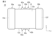
- FIG. 2 is a top view showing an example of a three-terminal multilayer ceramic capacitor according to an embodiment of the present invention.
- FIG. 3 is a front view showing an example of a three-terminal multilayer ceramic capacitor according to an embodiment of the present invention.
- FIG. 4 is a cross-sectional view taken along line IV-IV in FIG. 1.
- FIG. 5 is a cross-sectional view taken along line V-V in FIG. 1.
- FIG. 6 is a cross-sectional view taken along line VI-VI in FIG. 4.
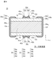
- FIG. 7 is a cross-sectional view taken along line VII-VII in FIG. 4.
- FIG. 8 is an enlarged photograph of the ⁇ portion in FIG. 7.
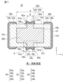
- FIG. 9 is an enlarged schematic view of the ⁇ portion in FIG. 7, showing the state of the protrusions and the dimensions of each portion.
- FIG. 10 is an enlarged schematic view of the ⁇ portion in FIG. 7, showing the state of bonding between the third external electrode and the third lead electrode portion.
- a three-terminal multilayer ceramic capacitor 10 includes, for example, a substantially rectangular parallelepiped laminate 12 and an external electrode 30.
- Laminate The laminate 12 has a plurality of laminated ceramic layers 14 and a plurality of internal electrode layers 16 laminated on the ceramic layers 14.
- the ceramic layers 14 and the internal electrode layers 16 are laminated in the height direction x.
- the laminate 12 has a first main surface 12a and a second main surface 12b facing the height direction x, a first side surface 12c and a second side surface 12d facing the width direction y perpendicular to the height direction x, and a first end surface 12e and a second end surface 12f facing the length direction z perpendicular to the height direction x and the width direction y.
- the corners and ridges of the laminate 12 are rounded. The corners are the portions where three adjacent surfaces of the laminate intersect, and the ridges are the portions where two adjacent surfaces of the laminate intersect.
- unevenness may be formed on a part or all of the first main surface 12a and the second main surface 12b, the first side surface 12c and the second side surface 12d, and the first end surface 12e and the second end surface 12f.
- the dimension L of the laminate 12 in the length direction z is not necessarily longer than the dimension W in the width direction y.
- the laminate 12 has an inner layer portion 18 and a first main surface side outer layer portion 20a and a second main surface side outer layer portion 20b arranged to sandwich the inner layer portion 18 in the stacking direction.
- the inner layer portion 18 includes a plurality of ceramic layers 14 and a plurality of internal electrode layers 16.
- the inner layer portion 18 includes the internal electrode layer 16 located closest to the first main surface 12a in the stacking direction to the internal electrode layer 16 located closest to the second main surface 12b.
- the internal electrode layer 16 has a first internal electrode layer 16a that is extended to the first end surface 12e and the second end surface 12f, and a second internal electrode layer 16b that is extended to the first side surface 12c and the second side surface 12d.
- the first internal electrode layers 16a and the second internal electrode layers 16b face each other via the ceramic layers 14.
- the inner layer portion 18 is a portion that generates electrostatic capacitance and essentially functions as a capacitor.
- the first main surface side outer layer portion 20a is located on the first main surface 12a side and is formed from a plurality of ceramic layers 14 located between the first main surface 12a and the outermost surface of the inner layer portion 18 on the first main surface 12a side and a straight line on that outermost surface (an extension line from the outermost surface to the first side surface 12c, the second side surface 12d, the first end surface 12e, and the second end surface 12f).
- the first main surface side outer layer portion 20a is an assembly of a plurality of ceramic layers 14 located between the first main surface 12a and the internal electrode layer 16 closest to the first main surface 12a.
- the ceramic layers 14 used in the first main surface side outer layer portion 20a may be the same as the ceramic layers 14 used in the inner layer portion 18.
- the second main surface side outer layer portion 20b is located on the second main surface 12b side and is formed from a plurality of ceramic layers 14 located between the second main surface 12b and the outermost surface of the inner layer portion 18 on the second main surface 12b side and a straight line on that outermost surface (an extension line from the outermost surface to the first side surface 12c, the second side surface 12d, the first end surface 12e, and the second end surface 12f).
- the second main surface side outer layer portion 20b is an assembly of a plurality of ceramic layers 14 located between the second main surface 12b and the internal electrode layer 16 closest to the second main surface 12b.
- the ceramic layers 14 used in the second main surface side outer layer portion 20b may be the same as the ceramic layers 14 used in the inner layer portion 18.
- the laminate 12 also has a first side surface outer layer portion 22a located on the first side surface 12c side and formed from a plurality of ceramic layers 14 located between the first side surface 12c and the outermost surface of the inner layer portion 18 on the first side surface 12c side.
- the laminate 12 has a second side outer layer portion 22b located on the second side 12d side and formed from a plurality of ceramic layers 14 located between the second side 12d and the outermost surface of the inner layer portion 18 on the second side 12d side.
- the first side surface outer layer portion 22a and the second side surface outer layer portion 22b are also called W gaps or side gaps.
- the laminate 12 has a first end face side outer layer portion 24a located on the first end face 12e side and formed from a plurality of ceramic layers 14 located between the first end face 12e and the outermost surface of the inner layer portion 18 on the first end face 12e side.
- the laminate 12 has a second end face side outer layer portion 24b located on the second end face 12f side and formed from a plurality of ceramic layers 14 located between the second end face 12f and the outermost surface of the inner layer portion 18 on the second end face 12f side.
- the first end surface side outer layer portion 24a and the second end surface side outer layer portion 24b are also referred to as an L gap or an end gap.
- the dimensions of the laminate 12 are not particularly limited.
- the ceramic layer 14 can be formed, for example, from a dielectric material as the ceramic material.
- a dielectric material for example, a dielectric ceramic containing a component such as BaTiO 3 , CaTiO 3 , SrTiO 3 , or CaZrO 3 can be used.
- a subcomponent such as a Mn compound, an Fe compound, a Cr compound, a Co compound, or a Ni compound may be added in a smaller amount than the main component depending on the desired characteristics of the laminate 12.
- the thickness of the ceramic layer 14 after firing is preferably 0.3 ⁇ m or more and 5.0 ⁇ m or less.
- the number of ceramic layers 14 to be stacked is preferably 5 or more and 2000 or less.
- the number of ceramic layers 14 is the total number of the ceramic layers 14 in the inner layer portion 18 and the ceramic layers 14 in the first main surface side outer layer portion 20a and the second main surface side outer layer portion 20b.
- the laminate 12 has a plurality of first internal electrode layers 16a and a plurality of second internal electrode layers 16b as the plurality of internal electrode layers 16.
- the plurality of first internal electrode layers 16a are disposed on the plurality of ceramic layers 14 and extend to the first end face 12e and the second end face 12f.
- the plurality of second internal electrode layers 16b are disposed on the plurality of ceramic layers 14 and extend to the first side face 12c and the second side face 12d.
- the plurality of first internal electrode layers 16a and the plurality of second internal electrode layers 16b may be alternately laminated with the ceramic layers 14 interposed therebetween, or a plurality of ceramic layers 14 on which the first internal electrode layers 16a are arranged may be laminated, and then a ceramic layer 14 on which the second internal electrode layers 16b are arranged may be laminated. In this way, the lamination pattern can be changed according to the capacitance value to be realized.
- the first internal electrode layer 16a includes a first opposing electrode portion 26a facing the second internal electrode layer 16b , a first extraction electrode portion 28a1 that is extracted from the first opposing electrode portion 26a to the surface of the first end face 12e of the laminate 12, and a second extraction electrode portion 28a2 that is extracted from the first opposing electrode portion 26a to the surface of the second end face 12f of the laminate 12.
- the first extraction electrode portion 28a1 is exposed on the surface of the first end face 12e of the laminate 12
- the second extraction electrode portion 28a2 is exposed on the surface of the second end face 12f of the laminate 12. Therefore, the first internal electrode layer 16a is not exposed on the surfaces of the first side face 12c and the second side face 12d of the laminate 12.
- the first lead-out electrode portion 28a.sub.1 is connected to a first external electrode 30a
- the second lead-out electrode portion 28a.sub.2 is connected to a second external electrode 30b.
- the shapes of the first opposing electrode portion 26a and the first and second lead-out electrode portions 28a1 and 28a2 are not particularly limited, but are preferably rectangular. However, the corners may be rounded.
- the length in the width direction y of the first extracted electrode portion 28a1 and the second extracted electrode portion 28a2 may be the same as the length in the width direction y of the first opposing electrode portion 26a, or may be formed to be shorter.
- the first lead electrode portion 28a1 and the second lead electrode portion 28a2 may have a tapered shape.
- the second internal electrode layer 16b is substantially cross-shaped and includes a second opposing electrode portion 26b opposing the first opposing electrode portion 26a, a third extraction electrode portion 28b1 extracted from the second opposing electrode portion 26b to the surface of the first side surface 12c of the laminate 12, and a fourth extraction electrode portion 28b2 extracted from the second opposing electrode portion 26b to the surface of the second side surface 12d of the laminate 12.
- the third extraction electrode portion 28b1 is exposed on the surface of the first side surface 12c of the laminate 12
- the fourth extraction electrode portion 28b2 is exposed on the surface of the second side surface 12d of the laminate 12. Therefore, the second internal electrode layer 16b is not exposed on the surface of the first end surface 12e and the surface of the second end surface 12f of the laminate 12.
- the third lead electrode portion 28b1 is connected to a third external electrode 30c
- the fourth lead electrode portion 28b2 is connected to a fourth external electrode 30d.
- the second counter electrode portion 26b and the third and fourth lead electrode portions 28b1 and 28b2 are preferably rectangular in shape, although the corners may be rounded.
- the relationship between a dimension A in the longitudinal direction z connecting the side of the second opposing electrode portion 26b on the first end face 12e side and the side of the second end face 12f side and a dimension B in the longitudinal direction z connecting the side of the third extraction electrode portion 28b1 and the fourth extraction electrode portion 28b2 on the first end face 12e side and the side of the second end face 12f side is A ⁇ B.
- the third extraction electrode portion 28b1 may have a tapered shape such that its width narrows toward the first side surface 12c, and the fourth extraction electrode portion 28b2 may have a tapered shape such that its width narrows toward the second side surface 12d.
- the laminate 12 has an opposing electrode region 27.
- the opposing electrode region 27 is a portion where the first opposing electrode portion 26a of the first internal electrode layer 16a and the second opposing electrode portion 26b of the second internal electrode layer 16b face each other.
- the opposing electrode region 27 is configured as a part of the inner layer portion 18.
- the opposing electrode region 27 is also called the effective portion of the capacitor.
- the first internal electrode layer 16a and the second internal electrode layer 16b are mainly composed of Ni and can be made of an appropriate conductive material such as metals such as Cu, Ag, Pd, and Au, or alloys containing at least one of these metals, such as an Ag-Pd alloy.
- first internal electrode layers 16a and second internal electrode layers 16b are not particularly limited, but it is preferable that the total number be, for example, 10 to 2000.
- the thickness of the first internal electrode layer 16a is not particularly limited, but is preferably, for example, about 0.30 ⁇ m or more and 1.0 ⁇ m or less.
- the thickness of the second internal electrode layer 16b is not particularly limited, but is preferably, for example, about 0.30 ⁇ m or more and 1.0 ⁇ m or less.
- External electrodes 30 are arranged on the first end face 12e side and the second end face 12f side, the first side face 12c side and the second side face 12d side, and the first principal face 12a side and the second principal face 12b side of the laminate 12.
- the external electrode 30 has a first external electrode 30a, a second external electrode 30b, a third external electrode 30c, and a fourth external electrode 30d.
- the first external electrode 30a is connected to the first internal electrode layer 16a and is disposed on the surface of the first end face 12e.
- the first external electrode 30a extends from the first end face 12e of the laminate 12 and is disposed on a part of the first main face 12a, a part of the second main face 12b, a part of the first side face 12c, and a part of the second side face 12d.
- the first external electrode 30a is electrically connected to the first lead electrode portion 28a 1 of the first internal electrode layer 16a.
- the first external electrode 30a may be disposed only on the surface of the first end face 12e.
- the second external electrode 30b is connected to the first internal electrode layer 16a and disposed on the surface of the second end face 12f.
- the second external electrode 30b extends from the second end face 12f of the laminate 12 and is disposed on a part of the first main face 12a and a part of the second main face 12b, as well as a part of the first side face 12c and a part of the second side face 12d.
- the second external electrode 30b is electrically connected to the second extraction electrode portion 28a2 of the first internal electrode layer 16a.
- the second external electrode 30b may be disposed only on the surface of the second end face 12f.
- the third external electrode 30c is connected to the second internal electrode layer 16b and is disposed on the surface of the first side surface 12c.
- the third external electrode 30c is electrically connected to the third extraction electrode portion 28b 1 of the second internal electrode layer 16b.
- the third external electrode 30c may extend from the first side surface 12c of the laminate 12 and be disposed on a part of the first main surface 12a and a part of the second main surface 12b.
- the third external electrode 30c of the present embodiment has a first outer convex portion (an example of a first convex portion) 42a and a second outer convex portion (an example of a second convex portion) 42b that conforms to the shape of the third underlying electrode layer 32c, since the third underlying electrode layer 32c has a first convex portion (an example of a first convex portion) 41a and a second convex portion (an example of a second convex portion) 41b, as described below.
- the fourth external electrode 30d is connected to the second internal electrode layer 16b and is disposed on the surface of the second side surface 12d.
- the fourth external electrode 30d is electrically connected to the fourth extraction electrode portion 28b2 of the second internal electrode layer 16b.
- the fourth external electrode 30d may extend from the second side surface 12d of the laminate 12 and be disposed on a part of the first main surface 12a and a part of the second main surface 12b.
- the fourth external electrode 30d of the present embodiment has a first outer convex portion (an example of a first convex portion) 42a and a second outer convex portion (an example of a second convex portion) 42b that conforms to the shape of the fourth underlying electrode layer 32d, since the fourth underlying electrode layer 32d has a first convex portion (an example of a first convex portion) 41a and a second convex portion (an example of a second convex portion) 41b, as described below.
- the first opposing electrode portion 26a of the first internal electrode layer 16a and the second opposing electrode portion 26b of the second internal electrode layer 16b face each other via the ceramic layer 14, forming a capacitance. Therefore, a capacitance can be obtained between the first external electrode 30a and the second external electrode 30b to which the first internal electrode layer 16a is connected, and the third external electrode 30c and the fourth external electrode 30d to which the second internal electrode layer 16b is connected, and the characteristics of a capacitor are expressed.
- the external electrode 30 includes a base electrode layer 32 containing a metal component and a glass component, and a plating layer 34 disposed on the surface of the base electrode layer 32.
- the base electrode layer 32 includes a first base electrode layer 32a, a second base electrode layer 32b, a third base electrode layer 32c, and a fourth base electrode layer 32d.
- the first base electrode layer 32a is connected to the first internal electrode layer 16a and is disposed on the surface of the first end face 12e.
- the first base electrode layer 32a also extends from the first end face 12e and is disposed on a part of the first main face 12a, a part of the second main face 12b, a part of the first side face 12c, and a part of the second side face 12d.
- the first base electrode layer 32a may be disposed only on the surface of the first end face 12e.
- the second base electrode layer 32b is connected to the first internal electrode layer 16a and is disposed on the surface of the second end face 12f.
- the second base electrode layer 32b extends from the second end face 12f and is disposed on a part of the first main face 12a and a part of the second main face 12b, as well as a part of the first side face 12c and a part of the second side face 12d.
- the second base electrode layer 32b may be disposed only on the surface of the second end face 12f.
- the third base electrode layer 32c is connected to the second internal electrode layer 16b and is disposed on the surface of the first side surface 12c.
- the third base electrode layer 32c may extend from the first side surface 12c and be disposed on a part of the first main surface 12a and a part of the second main surface 12b.
- the fourth base electrode layer 32d is connected to the second internal electrode layer 16b and is disposed on the surface of the second side surface 12d.
- the fourth base electrode layer 32d may extend from the second side surface 12d and be disposed on a part of the first main surface 12a and a part of the second main surface 12b.
- the third and fourth base electrode layers 32c and 32d each have a convex portion 41 including a first convex portion 41a and a second convex portion 41b, as shown in Figures 6 to 10.
- the characteristic shapes of the third and fourth base electrode layers 32c and 32d in this embodiment will be described in detail later.
- the base electrode layer 32 includes at least one selected from a baked layer, a conductive resin layer, etc. In the experimental examples described later, the base electrode layer 32 is a baked layer. Hereinafter, each configuration in the case where the base electrode layer 32 is the baked layer or the conductive resin layer will be described.
- the baking layer includes a glass component and a metal component.
- the glass component of the baking layer includes at least one selected from B, Si, Ba, Mg, Al, Li, etc.
- the metal component of the baking layer includes, for example, Cu as the main component and at least one selected from Ni, Ag, Pd, Ag-Pd alloy, Au, etc.
- the baking layer is formed by applying a conductive paste including a glass component and a metal component to the laminate 12 and baking it.
- the baking layer may be a layered chip having an internal electrode layer 16 and a ceramic layer 14 and a conductive paste applied to the laminated chip, which are simultaneously baked, or a layered chip having an internal electrode layer 16 and a ceramic layer 14 is baked to obtain the laminate 12, and then a conductive paste is baked on the laminate 12.
- the baking layer is formed by simultaneously baking the laminated chip having the internal electrode layer 16 and the ceramic layer 14 and the conductive paste applied to the laminated chip, it is preferable to bake the layer to which a dielectric material is added instead of the glass component.
- the baked layer may be multiple layers.
- the base electrode layer 32 contains a dielectric material instead of a glass component, the adhesion between the laminate 12 and the base electrode layer 32 can be improved.
- the base electrode layer 32 may contain both a glass component and a dielectric component.
- the dielectric material contained in the base electrode layer 32 may be the same as or a different type of dielectric material as the ceramic layer 14.
- the dielectric component contains at least one selected from the group consisting of BaTiO3 , CaTiO3 , (Ba,Ca) TiO3 , SrTiO3 , and CaZrO3 .
- the base electrode layer is a conductive resin layer
- the conductive resin layer may be disposed on the baked layer so as to cover the baked layer, or may be disposed directly on the laminate 12 without providing a baked layer.
- the conductive resin layer contains metal such as conductive particles and a thermosetting resin.
- the conductive resin layer may completely cover the underlying electrode layer, or may cover only a part of the underlying electrode layer.
- the conductive resin layer contains a thermosetting resin, and is therefore more flexible than a conductive layer made of, for example, a plating film or a fired conductive paste. Therefore, even if the three-terminal multilayer ceramic capacitor 10 is subjected to a physical shock or a shock caused by a thermal cycle, the conductive resin layer functions as a buffer layer and can prevent cracks in the three-terminal multilayer ceramic capacitor 10.
- the metal contained in the conductive resin layer may be Cu as a main component, and Ag, Ni, Sn, Bi, or an alloy containing any of these may be used. Metal powders whose surfaces are coated with Ag can also be used. When using metal powders whose surfaces are coated with Ag, it is preferable to use Cu, Ni, Sn, Bi or alloy powders thereof as the metal powder.
- Ag conductive metal powder is used as the conductive metal is that Ag has the lowest resistivity among metals and is therefore suitable as an electrode material, and Ag is a noble metal and therefore does not oxidize and has high weather resistance. In addition, it is possible to make the base metal inexpensive while maintaining the above-mentioned characteristics of Ag.
- the metal contained in the conductive resin layer may be Cu or Ni that has been subjected to an anti-oxidation treatment.
- a metal powder having a surface coated with Sn, Ni, or Cu can also be used.
- Ag, Cu, Ni, Sn, Bi, or an alloy powder thereof it is preferable to use Ag, Cu, Ni, Sn, Bi, or an alloy powder thereof as the metal powder.
- the metal contained in the conductive resin layer is mainly responsible for the electrical conductivity of the conductive resin layer. Specifically, when the conductive fillers come into contact with each other, an electrical path is formed inside the conductive resin layer.
- the metal contained in the conductive resin layer can be spherical or flat, but it is preferable to use a mixture of spherical metal powder and flat metal powder.
- thermosetting resins such as epoxy resin, phenoxy resin, phenolic resin, urethane resin, silicone resin, polyimide resin, etc.
- epoxy resin which has excellent heat resistance, moisture resistance, and adhesion, is one of the most suitable resins.
- the conductive resin layer preferably contains a curing agent in addition to the thermosetting resin.
- a curing agent in addition to the thermosetting resin.
- various known compounds such as phenol-based, amine-based, acid anhydride-based, imidazole-based, active ester-based, and amide-imide-based compounds can be used as the curing agent for the epoxy resin.
- the conductive resin layer may be multiple layers.
- the plating layer 34 includes a first plating layer 34a, a second plating layer 34b, a third plating layer 34c, and a fourth plating layer 34d.
- the first plating layer 34a, the second plating layer 34b, the third plating layer 34c, and the fourth plating layer 34d which are plating layers 34 that can be disposed on the base electrode layer 32, will be described with reference to FIGS. 4 and 5.
- the first plating layer 34a, the second plating layer 34b, the third plating layer 34c and the fourth plating layer 34d each contain at least one selected from, for example, Cu, Ni, Sn, Ag, Pd, an Ag-Pd alloy, Au and the like.
- the first plating layer 34a is disposed so as to cover the first base electrode layer 32a.
- the second plating layer 34b is disposed so as to cover the second base electrode layer 32b.
- the third plating layer 34c is disposed so as to cover the third base electrode layer 32c.
- the fourth plating layer 34d is disposed so as to cover the fourth base electrode layer 32d.
- the third and fourth plating layers 34c and 34d each have an outer convex portion 42 corresponding to the convex portion 41 of the third and fourth base electrode layers 32c and 32d. That is, the third and fourth plating layers 34c and 34d each have a first outer convex portion 42a and a second outer convex portion 42b along the shapes of the first convex portion 41a and the second convex portion 41b of the third and fourth base electrode layers 32c.
- the third and fourth plating layers 34c and 34d form the outer surfaces of the third and fourth external electrodes 30c and 30d
- the first and second outer convex portions 42a and 42b of the third and fourth plating layers 34c and 34d become the first and second outer convex portions 42a and 42b of the third and fourth external electrodes 30c and 30d.
- the first plating layer 34a, the second plating layer 34b, the third plating layer 34c, and the fourth plating layer 34d may be formed of multiple layers.
- the plating layer 34 has a two-layer structure of a lower plating layer made of Ni plating formed on the base electrode layer 32, and an upper plating layer made of Sn plating formed on the lower plating layer.
- the first plating layer 34a has a first lower plating layer and a first upper plating layer located on the surface of the first lower plating layer.
- the second plating layer 34b has a second lower plating layer and a second upper plating layer located on the surface of the second lower plating layer.
- the third plating layer 34c has a third lower plating layer and a third upper plating layer located on the surface of the third lower plating layer.
- the fourth plating layer 34d has a fourth lower plating layer and a fourth upper plating layer located on the surface of the fourth lower plating layer.
- the lower plating layer made of Ni plating is used to prevent the base electrode layer 32 from being eroded by solder when mounting the three-terminal multilayer ceramic capacitor 10, and the upper plating layer made of Sn plating is used to improve the wettability of the solder when mounting the three-terminal multilayer ceramic capacitor 10, making it easier to mount.
- the thickness of each plating layer is preferably 2.0 ⁇ m or more and 15.0 ⁇ m or less.
- Figures 8 to 10 show the cross-sectional shapes of the laminate 12 and the third underlying electrode layer 32c in a cross-sectional view along the first and second main surfaces 12a, 12b.
- Figures 8 to 10 show, for example, an LW cross section (a cross section including the length direction z and width direction y) at 1/2T, where T is the dimension of the three-terminal multilayer ceramic capacitor 10 in the height direction x.
- a third base electrode layer 32c is formed on the first side surface 12c of the laminate 12 in the LW cross section.
- the third base electrode layer 32c has a central portion 40 and a protruding portion 41.
- the central portion 40 is the third base electrode layer 32c in a portion located at point M, which is the center in the longitudinal direction z of the third base electrode layer 32c, and has a thickness of 3 ⁇ m or more in the width direction y relative to the first side surface 12c.
- the protruding portion 41 includes a first protruding portion 41a and a second protruding portion 41b.
- the first convex portion 41a is a portion of the third base electrode layer 32c that is located at point Q1, which is a portion of the third base electrode layer 32c that is thicker in the width direction y relative to the first side surface 12c than the central portion 40 and is closer to the first end surface 12e than the central portion 40.
- the second convex portion 41b is a portion of the third base electrode layer 32c that is located at point Q2, which is closer to the second end face 12f than the central portion 40 and has a thickness in the width direction y relative to the first side surface 12c that is greater than the central portion 40.
- At least one of the first and second protrusions 41a, 41b has the largest thickness in the third base electrode layer 32c.
- the third base electrode layer 32c has a limit point 45 where the thickness is 3 ⁇ m or more from the base electrode end 35, which is the end of the third base electrode layer 32c.
- the base electrode end 35 includes a first base electrode end 35a on the first end surface 12e side of the third base electrode layer 32c and a second base electrode end 35b on the second end surface 12f side.
- the first base electrode end (corresponding to the first external electrode end) 35a is the end of the third base electrode layer 32c on the first end surface 12e side.
- the second base electrode end (corresponding to the second external electrode end) 35b is the end of the third base electrode layer 32c on the second end surface 12f side.
- the limit point 45 includes a first limit point 45a and a second limit point 45b.
- the first limit point 45a is the third base electrode layer 32c located at point P1 on the first end face 12e side. At point P1, the first limit point 45a is the point where the thickness in the width direction y relative to the first side face 12c becomes 3 ⁇ m or more for the first time from the first base electrode end portion 35a (point R1).
- the second limit point 45b is the portion of the third base electrode layer 32c located at point P2 on the second end face 12f side. At point P2, the second limit point 45b is the point where the thickness in the width direction y relative to the first side face 12c becomes 3 ⁇ m or more for the first time from the second base electrode end portion 35b (point R2).
- the third extracted electrode portion 28b1 is located between the first limit point 45a and the second limit point 45b.
- the extracted end portion 29 (the first extracted end portion 29a on the first end face 12e side and the second extracted end portion 29b on the second end face 12f side) of the third extracted electrode portion 28b1 is located between the first limit point 45a and the second limit point 45b.
- the third base electrode layer 32c can be said to have a central region 50c, a first end face side region 50a, and a second end face side region 50b.
- the central region 50c is a region including the center portion 40, and is a region between the first convex portion 41a and the second convex portion 41b.
- the first end face side region 50a is a region on the first end face 12e side with respect to the central region 50c.
- the second end face side region 50b is a region on the second end face 12f side with respect to the central region 50c.
- the first convex portion 41a is located at the boundary between the central region 50c and the first end face side region 50a.
- the second convex portion 41b is located at the boundary between the central region 50c and the second end face side region 50b.
- the first limit point 45a is located within the first end face side region 50a.
- the second limit point 45b is located within the second end surface side region 50b.
- the first convex portion 41a and the second convex portion 41b are thicker than the central portion 40 and are the thickest in the third base electrode layer 32c.
- the thickness of the third base electrode layer 32c decreases from the first convex portion 41a to the first base electrode end portion 35a, but since the thickness of the first convex portion 41a is large, the first limit point 45a can be provided closer to the first end surface 12e side than the first convex portion 41a.
- the thickness of the third base electrode layer 32c decreases from the second convex portion 41b to the second base electrode end portion 35b, but since the thickness of the second convex portion 41b is large, the second limit point 45b can be provided closer to the second end surface 12f side than the second convex portion 41b.
- the distance a1 from the first base electrode end 35a (point R1) to the first convex portion 41a (point Q1) and the distance a2 from the second base electrode end 35b (point R2) to the second convex portion 41b (point Q2) are a, it is preferable that 0.10 ⁇ a/e ⁇ 0.30.
- the thickness d1 of the first convex portion 41a in the width direction y relative to the first side surface 12c and the thickness d2 of the second convex portion 41b in the width direction y relative to the first side surface 12c are d, and the thickness of the central portion 40 in the width direction y relative to the first side surface 12c is c, it is preferable that 0.65 ⁇ c/d ⁇ 0.97.
- the thickness c of the central portion 40 is 8.0 ⁇ m ⁇ c ⁇ 18.0 ⁇ m.
- the thickness d of the first and second protrusions 41a and 41b is 10.0 ⁇ m ⁇ d ⁇ 21.0 ⁇ m.
- the width e of the third base electrode layer 32c is preferably 200 ⁇ m ⁇ e ⁇ 600 ⁇ m. It is more preferable that the width e is 230 ⁇ m ⁇ e ⁇ 390 ⁇ m.
- the alloy layer 62 and the glass ratio formed between the third base electrode layer 32c and the third lead electrode portion 28b1 will be described.
- the third base electrode layer 32c and the third lead electrode portion 28b1 are in contact with each other and joined at a contact interface 60a of the first side surface 12c.
- Ni in the third lead electrode portion 28b1 and Cu in the third base electrode layer 32c are mutually diffused to form an alloy layer 62.
- This alloy layer 62 is formed more densely than the third lead electrode portion 28b1 and the third base electrode layer 32c themselves, and improves the joining strength between the third lead electrode portion 28b1 and the third base electrode layer 32c.
- the third base electrode layer 32c has a contact region 60 and a non-contact region 61.
- the contact region 60 includes a contact interface 60a and an outside-interface region 60b.
- the contact interface 60a is an interface where the third base electrode layer 32c is in contact with the third lead electrode portion 28b1 .
- An alloy layer 62 is formed at the contact interface 60a.
- the contact region 60 is a portion of the third base electrode layer 32c extending from the contact interface 60a to the outside in the width direction y.
- the outside-interface region 60b is a region in the contact region 60 excluding the contact interface 60a. In other words, the outside-interface region 60b is a region in the contact region 60 excluding the region where the alloy layer 62 is formed.
- the non-contact region 61 is a portion of the third base electrode layer 32c other than the contact region 60, and is a region where the third base electrode layer 32c is not in contact with the third lead electrode portion 28b1 .
- the non-contact region 61 has a first non-contact region 61a located closer to the first end face 12e than the contact region 60, and a second non-contact region 61b located closer to the second end face 12f than the contact region 60.
- the contact region 60 is located between the first convex portion 41a and the second convex portion 41b.
- the contact region 60 since the third extraction electrode portion 28b1 only needs to be positioned so as to be contained between the first limit point 45a and the second limit point 45b, the contact region 60 only needs to be formed between the first limit point 45a and the second limit point 45b. It is preferable that the central portion 40 is included in the contact region 60.
- the out-of-interface region glass ratio which is the ratio of the glass component to the components constituting the third base electrode layer 32c in the out-of-interface region 60b
- the non-contact region glass ratio which is the ratio of the glass component to the components constituting the third base electrode layer 32c in the non-contact region 61
- the first non-contact region glass ratio which is the ratio of the glass component to the components constituting the third base electrode layer 32c in the first non-contact region 61a
- the second non-contact region glass ratio which is the ratio of the glass component to the components constituting the third base electrode layer 32c in the second non-contact region 61b
- the outer-interface region glass ratio g1 is 1.4 times or more and 1.7 times or less than the non-contact region glass ratio g2 (the average of the first non-contact region glass ratio g2a and the second non-contact region glass ratio g2b).
- the fourth base electrode layer 32d has the same configuration as the third base electrode layer 32c, and will be briefly described below.
- the fourth base electrode layer 32d has a central portion 40 whose thickness from the second side surface 12d is 3 ⁇ m or more, and a convex portion 41 including a first convex portion 41a and a second convex portion 41b.
- the fourth base electrode layer 32d also has a first limit point 45a where the thickness from the first base electrode end portion 35a of the fourth base electrode layer 32d to the second side surface 12d becomes 3 ⁇ m or more, and a second limit point 45b where the thickness from the second base electrode end portion 35b of the fourth base electrode layer 32d to the second side surface 12d becomes 3 ⁇ m or more.
- the fourth extraction electrode portion 28b 2 is located between the first limit point 45a and the second limit point 45b. Specifically, in the laminate 12, the first extraction end portion 29a on the first end face 12e side and the second extraction end portion 29b on the second end face 12f side of the fourth extraction electrode portion 28b2 are located between the first limit point 45a and the second limit point 45b.
- the dimension in the length direction z of the three-terminal multilayer ceramic capacitor 10 including the laminate 12 and the first external electrode 30a to the fourth external electrode 30d is defined as dimension L
- the dimension in the height direction x is defined as dimension T
- the dimension in the width direction y is defined as dimension W.
- the dimensions of the three-terminal multilayer ceramic capacitor 10 are not particularly limited, but the L dimension in the length direction z is 1.05 mm to 1.35 mm
- the T dimension in the height direction x is 0.45 mm to 0.90 mm
- the W dimension in the width direction y is 0.60 mm to 0.95 mm.
- the dimensions of the three-terminal multilayer ceramic capacitor 10 can be measured using a microscope.
- a dielectric sheet for the ceramic layer and a conductive paste for the internal electrode layer are prepared.
- the dielectric sheet and the conductive paste for the internal electrode layer contain a binder and a solvent.
- the binder and the solvent may be publicly known.
- a conductive paste for the internal electrode layers is printed in a predetermined pattern on the dielectric sheet, for example by gravure printing or screen printing. This prepares a dielectric sheet on which the pattern of the first internal electrode layer is formed, and a dielectric sheet on which the pattern of the second internal electrode layer is formed.
- a predetermined number of dielectric sheets for the outer layer, on which the pattern of the internal electrode layer is not printed, are stacked on top of this portion that will become the inner layer portion to form a portion that will become the first main surface outer layer portion on the first main surface side. In this way, a laminated sheet is produced.
- the laminated sheets are pressed in the stacking direction using a means such as a hydrostatic press to produce a laminated block.
- the laminated block is cut to a predetermined size to produce laminated chips.
- the corners and edges of the laminated chips may be rounded by barrel polishing or the like.
- the firing temperature depends on the materials of the ceramic layers and the internal electrode layers, but is preferably 900°C or higher and 1400°C or lower.
- a third base electrode layer 32c of a third external electrode 30c is formed on a first side surface 12c of the laminate 12 obtained by firing, and a fourth base electrode layer 32d of a fourth external electrode 30d is formed on a second side surface 12d of the laminate 12.
- the third and fourth base electrode layers 32c, 32d having the first convex portion 41a and the second convex portion 41b can be formed, for example, by applying the external electrode paste 70 twice using a roller transfer method.
- FIG. 11 (a) is a process diagram showing the first application process of applying the first paste layer to the laminate, and (b) is a process diagram showing the second application process of applying the second paste layer to the laminate.
- the first coating process is performed by a first coating mechanism 90.
- the first coating mechanism 90 includes a first supply roller 91 having a plurality of first recesses 92, a first coating roller 93, a first paste tank 94 in which the external electrode paste 70 is stored, and a first carrier tape 95 for transporting the laminate 12.
- the first supply roller 91 rotates, a portion of the roller is immersed in the external electrode paste 70 in the first paste tank 94, so that the external electrode paste 70 adheres to the plurality of first recesses 92 in sequence.
- the first recess 92 has a shape that allows the first first paste layer 71 to be formed on the first side surface 12c or the second side surface 12d of the laminate 12. In the example of FIG.
- the first recess 92 is formed from one recess having a flat bottom surface, and the first recess 92 forms the first paste layer 71 as a continuous layer.
- the external electrode paste 70 in the first recess 92 of the first supply roller 91 is transferred as a first paste layer 71 to the outer peripheral surface of the rotating first application roller 93.
- the first paste layer 71 is applied in a flat manner to the first side surface 12c or the second side surface 12d of each of the multiple laminates 12 that are transported sequentially along the first carrier tape 95.
- the second coating mechanism 90a has a second supply roller 91a having a plurality of second recesses 92a, a second coating roller 93a, a second paste tank 94a in which the external electrode paste 70 is stored, and a second carrier tape 95a that transports the laminate 12 to which the first paste layer 71 has been applied.
- a second supply roller 91a rotates, a portion of it is immersed in the external electrode paste 70 in the second paste tank 94a, so that the external electrode paste 70 adheres sequentially to the plurality of second recesses 92a.
- the second recesses 92a have a shape that allows a second second paste layer 72 to be formed on the first paste layer 71 of the laminate 12.
- the second recess 92a is formed by dividing one recess into two along the rotation direction, and the second paste layer 72 is formed as a layer divided into two along the rotation direction by the second recess 92a.
- the external electrode paste 70 in the second recess 92a of the second supply roller 91a is transferred as the second paste layer 72 to the outer circumferential surface of the rotating second application roller 93a. Then, the second paste layer 72 is applied onto the first paste layer 71 of the multiple laminates 12 that are sequentially transported along the second carrier tape 95a.
- the second paste layer 72 divided into two is applied to both ends of the first paste layer 71.
- the thickness of the paste layer is large in the portion where the first paste layer 71 and the second paste layer 72 are laminated, and the thickness of the paste layer is small in the portion where only the first paste layer 71 is between the second paste layer 72 and the second paste layer 72.
- a base electrode layer 32 is formed having a first protrusion 41a and a second protrusion 41b that are thicker at both ends than at the center.
- the external electrode paste 70 can also be applied to the laminate 12 by extruding it through a slit of the desired shape.
- the external electrode paste 70 may be any paste capable of forming the third and fourth base electrode layers 32c, 32d having the above-mentioned shapes.
- the external electrode paste 70 is preferably one that can suppress swelling of the center compared to the ends when the base electrode layer 32 is formed using the external electrode paste 70.
- the external electrode paste 70 contains a resin, a metal filler, and a solvent, which suppresses the expansion of the central portion 40 in the third and fourth base electrode layers 32c and 32d, suppresses an increase in the dimensions of the three-terminal multilayer ceramic capacitor 10, and allows the capacitor to be made thinner and smaller, and also makes it easier to form the first and second protrusions 41a and 41b.
- the type of resin is not particularly limited as long as the desired effect is not hindered.
- various resins that have conventionally been blended in the external electrode paste 70 can be used without any particular limitation.
- preferred resins include cellulose-based resins, acrylic resins, and butyral-based resins.
- the resin contains a cellulose-based resin, since it is easy to obtain the external electrode paste 70 having a viscosity suitable for forming the external electrodes.
- the resin contains a copolymer resin having a block derived from a cellulose-based resin.
- Such a copolymer resin may be a block copolymer or a graft copolymer.
- the cellulose-based resin is, for example, at least one of ethyl cellulose, methyl cellulose, hydroxypropyl cellulose, trityl cellulose, acetyl cellulose, carboxymethyl cellulose, and nitrocellulose.
- Acrylic resins are homopolymers or copolymers of one or more monomers, such as isobutyl methacrylate, methyl methacrylate, hydroxyethyl methacrylate, hydroxypropyl methacrylate, n-butyl methacrylate, and 2-ethylhexyl methacrylate.
- the metal filler is made of the metal that constitutes the external electrodes.
- the type of metal that constitutes the metal filler is appropriately selected depending on the type of metal that constitutes the external electrodes.
- copper (Cu), silver (Ag), nickel (Ni), or an alloy containing these metals is preferred because of its excellent electrical conductivity and the ease of obtaining a metal filler with a desired particle size.
- the alloy containing these metals preferably contains one or more selected from the group consisting of copper (Cu), silver (Ag), and nickel (Ni). It is also preferred that the alloy containing these metals contains tin (Sn).
- the solvent is added as a component that dissolves the resin, disperses the metal filler, and gives fluidity to the external electrode paste 70.
- the solvent includes one or more first solvents and one or more second solvents.
- the ratio of the mass of the first solvent to the mass of the solvent and the ratio of the mass of the second solvent to the mass of the solvent are each 40 mass % or more.
- the lowest boiling point T Hl among the boiling points of the one or more second solvents under atmospheric pressure is higher by 10° C. or more than the highest boiling point T Lh among the boiling points of the one or more first solvents under atmospheric pressure.
- the highest boiling point T Hh among the boiling points of the one or more second solvents under atmospheric pressure is T Hl +10° C. or less.
- the lowest boiling point T Ll among the boiling points under atmospheric pressure of the one or more first solvents is T Lh -10°C or more.
- the solvent may contain a sub-solvent in addition to the first solvent and the second solvent.
- the boiling point of the auxiliary solvent at atmospheric pressure is less than (T Ll - 10)°C, greater than (T Lh + 10)°C and less than (T Hl - 10)°C, or greater than (T Hh + 10)°C.
- suitable solvents include Texanol, propylene glycol monophenyl ether, butyl carbitol, terpene solvents, diethylene glycol, carbitol acetate, butyl carbitol acetate, benzyl alcohol, methyl propylene diglycol, diphenyl ether, and ethylene glycol.
- the external electrode paste 70 also contains a resin containing an ethyl cellulose-based resin and an acrylic-based resin, at least a portion of which is copolymerized, a Cu filler, and a solvent. It is preferable that the interfacial tension generated between the resin and the solvent is 15 mN/m or more.
- the resin and the solvent are as described above.
- the base electrode layer 32 is a baked layer or a conductive resin layer.
- a conductive paste (external electrode paste 70) containing a glass component and a metal component is applied.
- the conductive paste can be applied, for example, by the first and second application steps described above.
- a baking process is performed to form the base electrode layers.
- the temperature of the baking process at this time is preferably 700° C. or higher and 900° C. or lower.
- the base electrode layer 32 was formed as a baked layer.
- the roller transfer method when forming the base electrode layer 32 not only on the first side surface 12c and the second side surface 12d but also on a part of the first main surface 12a and a part of the second main surface 12b, it is possible to form the base electrode layer 32 on a part of the first main surface 12a and a part of the second main surface 12b by increasing the pressing pressure when the external electrode paste 70 is roller transferred.
- the external electrode paste 70 is applied by extruding it through a slit, by increasing the amount of external electrode paste 70 extruded, it is possible to form the base electrode layer 32 not only on the first side surface 12c and the second side surface 12d, but also on a portion of the first principal surface 12a and a portion of the second principal surface 12b.
- the conductive resin layer can be formed by the following method.
- the conductive resin layer may be formed on the surface of the baked layer, or the conductive resin layer may be formed directly on the laminate 12 without forming a baked layer.
- the conductive resin layer is formed by applying a conductive resin paste (external electrode paste 70) containing a thermosetting resin and a metal component onto the baked layer or the laminate 12.
- the conductive resin paste can be applied, for example, by the first and second application steps described above.
- a heat treatment is performed at a temperature of 250°C to 550°C to thermally cure the resin and form a conductive resin layer.
- the atmosphere during this heat treatment is preferably an N2 atmosphere.
- the conductive resin paste can be applied in the same manner as the method for forming the base electrode layer 32 as a baked layer, for example, by extruding the conductive resin paste through a slit and applying it, or by using a roller transfer method.
- the first base electrode layer 32a of the first external electrode 30a is formed on the first end face 12e of the fired laminate, and the second base electrode layer 32b of the second external electrode 30b is formed on the second end face 12f.
- a conductive paste containing a glass component and a metal component is applied, and then a baking process is performed to form the base electrode layers.
- the baking process temperature is preferably 700° C. or higher and 900° C. or lower.
- the conductive paste is applied to both end faces of the laminate by, for example, a dipping method, a screen printing method, etc.
- the first base electrode layer 32a and the second base electrode layer 32b were formed by the dipping method so as to extend not only to the first end face 12e and the second end face 12f but also to a part of the first main face 12a, a part of the second main face 12b, a part of the first side face 12c, and a part of the second side face 12d.
- the third base electrode layer 32c, the fourth base electrode layer 32d, the first base electrode layer 32a, and the second base electrode layer 32b may be baked simultaneously, or the side surfaces 12c and 12d and the end surfaces 12e and 12f may be baked separately.
- the baked layer may contain a dielectric component.
- the dielectric component may be contained instead of the glass component, or both may be contained.
- the dielectric component is preferably, for example, the same type of dielectric material as the laminate.
- the baked layer contains a dielectric component, it is preferable to apply a conductive paste to the laminated chip before firing, and simultaneously bake (fire) the laminated chip before firing and the conductive paste applied to the laminated chip before firing to form a laminate with a baked layer.
- the temperature of the baking process (firing temperature) at this time is preferably 900°C or higher and 1400°C or lower.
- the plating layer 34 is formed.
- the plating layer 34 may be formed on the surface of the base electrode layer 32, or may be formed directly on the laminate 12. In the experimental example described below, the plating layer 34 was formed on the surface of the base electrode layer 32. More specifically, a Ni plating layer is formed on the base electrode layer 32 as the lower plating layer, and a Sn plating layer is formed as the upper plating layer. The Ni plating layer and the Sn plating layer are formed sequentially, for example, by barrel plating. Either electrolytic plating or electroless plating may be used for plating. However, electroless plating has the disadvantage that pretreatment with a catalyst or the like is required to improve the plating deposition speed, which complicates the process. Therefore, it is usually preferable to use electrolytic plating.
- the three-terminal multilayer ceramic capacitor 10 according to this embodiment is manufactured.
- the third and fourth base electrode layers 32c, 32d having the first and second convex parts 41a, 41b have a large range of thicknesses of 3 ⁇ m or more. Therefore, the tolerance of the positional deviation of the second internal electrode layer 16b with respect to the third and fourth base electrode layers 32c, 32d is large, and the moisture resistance reliability can be improved. This will be specifically described below.
- the third and fourth base electrode layers 32c, 32d have a first convex portion 41a on the first end face 12e side and a second convex portion 41b on the second end face 12f side, which are thicker than the central portion 40 having a thickness of 3 ⁇ m or more. Therefore, the third and fourth base electrode layers 32c, 32d having the first and second convex portions 41a, 41b are thicker on the first and second end faces 12e, 12f side than the third and fourth base electrode layers 32c, 32d not having the first and second convex portions 41a, 41b, for example, which are thickest at the central portion 40 and become thinner toward the first and second end faces 12e, 12f side. This point will be further explained using FIG. 12.
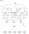
- FIG. 12 is a schematic diagram for explaining the difference in configuration between the three-terminal multilayer ceramic capacitor according to the embodiment of the present invention and an existing three-terminal multilayer ceramic capacitor.
- the third base electrode layer 32c according to the present embodiment is shown by a solid line
- the third base electrode layer of the existing three-terminal multilayer ceramic capacitor (hereinafter referred to as the existing base electrode layer) is shown by a broken line.
- the third base electrode layer 32c according to the present embodiment has a center portion 40 at point M and first and second convex portions 41a, 41b at points Q1 and Q2, and the thickness of the first and second convex portions 41a, 41b is d.
- the thickness d of the first and second convex portions 41a, 41b is the largest in the third base electrode layer 32c.
- the third base electrode layer 32c according to the present embodiment has a first limit point 45a at point P1 between the first convex portion 41a and the first base electrode end portion 35a at point R1, and a second limit point 45b at point P2 between the second convex portion 41b and the second base electrode end portion 35b at point R2.
- the thickness h of the first and second limit points 45a, 45b is 3 ⁇ m.
- the existing base electrode layer has one apex 80 at point M.
- the thickness at apex 80 is d, the same as that of the first and second protrusions 41a, 41b.
- the existing base electrode layer also has first and second base electrode ends at points R1 and R2. According to FIG. 12, in the existing base electrode layer, the first times when the thickness of the existing base electrode layer becomes 3 ⁇ m or more from the first and second base electrode ends (points R1, R2) are points S1 and S2 of the reference limit point 81 (first reference limit point 81a, second reference limit point 81b).
- the range from the first limit point 45a to the second limit point 45b of the third base electrode layer 32c according to this embodiment is from point P1 to point P2, whereas the range from the first reference limit point 81a to the second reference limit point 81b of the existing base electrode layer is from point S1 to point S2.
- the range from point P1 to point P2 > the range from point S1 to point S2.
- the first limit point 45a where the thickness becomes 3 ⁇ m or more from the first base electrode end 35a
- the second limit point 45b where the thickness becomes 3 ⁇ m or more from the second base electrode end 35b
- the range from the first limit point 45a to the second limit point 45b, where the thickness is 3 ⁇ m or more, is large, it is easy to position the first and second lead ends 29a, 29b within the range between the first limit point 45a and the second limit point 45b.
- the tolerance of the positional deviation of the second internal electrode layer 16b with respect to the third and fourth base electrode layers 32c, 32d can be increased. Therefore, it is possible to prevent at least a portion of the third and fourth extraction electrode portions 28b1 , 28b2 from being positioned out of position, such as being positioned outside the third and fourth base electrode layers 32c, 32d, and as a result, it is possible to prevent moisture from penetrating into the laminate 12 through the third and fourth extraction electrode portions 28b1 , 28b2, thereby improving the moisture resistance reliability.
- the distance f from the first and second base electrode ends 35a, 35b to the first and second limit points 45a, 45b is small, 0.01 or more and 0.09 or less, relative to the width e of the third and fourth base electrode layers 32c, 32d. This is considered to be because the third and fourth base electrode layers 32c, 32d are formed with a large inclination from the first and second base electrode ends 35a, 35b to a thickness of 3 ⁇ m or more so as to have the first and second convex parts 41a, 41b.
- the tolerance of the positional deviation of the second internal electrode layer 16b with respect to the third and fourth base electrode layers 32c, 32d is large. Therefore, it is possible to further prevent the third and fourth lead electrode portions 28b 1 , 28b 2 from being misaligned with respect to the third and fourth base electrode layers 32c, 32d, and it is possible to further improve the moisture resistance reliability.
- the distance a from the first and second base electrode ends 35a, 35b to the first and second protrusions 41a, 41b is 0.10 or more and 0.30 or less relative to the width e of the third and fourth base electrode layers 32c, 32d. This makes it possible to make the distance f from the first and second base electrode ends 35a, 35b to the first and second limit points 45a, 45b at which the thickness becomes 3 ⁇ m or more smaller relative to the width e of the third and fourth base electrode layers 32c, 32d.
- the range from the first limit point 45a to the second limit point 45b is large, it is possible to further suppress the third and fourth extraction electrode parts 28b 1 , 28b 2 from being misaligned with respect to the third and fourth base electrode layers 32c, 32d, and the moisture resistance reliability can be further improved.
- the third and fourth base electrode layers 32c, 32d can have the first convex portion 41a and the second convex portion 41b at positions close to the first and second end faces 12e, 12f, respectively. This makes it possible to increase the range from the first limit point 45a to the second limit point 45b, where the thickness is 3 ⁇ m or more. Therefore, it is possible to further prevent the third and fourth extraction electrode portions 28b 1 , 28b 2 from being misaligned with respect to the third and fourth base electrode layers 32c, 32d, and it is possible to further improve the moisture resistance reliability.
- the thickness c of the central portion 40 is in the above range. Therefore, the thickness c can be set to 3 ⁇ m or more to ensure moisture resistance reliability, while preventing the thickness c from becoming too thick. This makes it possible to suppress an increase in the dimensions of the three-terminal multilayer ceramic capacitor 10 while ensuring moisture resistance reliability, thereby making it possible to reduce the thickness and size.
- the thickness d of the first and second protrusions 41 a, 41 b is in the above range.
- the thickness d is set to 3 ⁇ m or more to ensure moisture resistance reliability, and the range from the first limit point 45 a to the second limit point 45 b can be enlarged while preventing the thickness d from becoming too thick. This makes it possible to suppress an increase in the dimensions of the three-terminal multilayer ceramic capacitor 10 while ensuring moisture resistance reliability, thereby making it possible to reduce the thickness and size.
- the glass components of the third and fourth base electrode layers 32c and 32d are concentrated in the outer-interface region 60b, which is a portion in the third and fourth base electrode layers 32c and 32d that is away from the contact interface 60a in the width direction y, to form a dense glass layer. Therefore, the outer-interface region glass ratio g1 is higher than the non-contact region glass ratio g2. Since the outer-interface region glass ratio g1 is relatively large, sintering tends to progress easily during firing in the outer-interface region 60b due to the presence of glass. Therefore, it is possible to suppress the rise in the contact region 60 and suppress the increase in the dimensions of the three-terminal multilayer ceramic capacitor 10, and it is also easy to form the first and second protrusions 41a and 41b by suppressing the rise in the contact region 60.
- the third and fourth extraction electrode portions 28b1 , 28b2 are in contact with the third and fourth base electrode layers 32c, 32d in the contact region 60 including the central portion 40.
- the glass components of the third and fourth base electrode layers 32c, 32d are concentrated in the outer interface region 60b away from the contact interface 60a in the width direction y in the third and fourth base electrode layers 32c, 32d to form a dense glass layer. Since the presence of glass components tends to facilitate sintering during firing, the contact region 60 including the central portion 40 is likely to have a more recessed shape than the first and second protruding portions 41a, 41b in a cross-sectional view along the first and second main surfaces 12a, 12b.
- the first and second non-contact regions 61a, 61b are less likely to have a concave shape due to the low non-contact region glass ratio g2, and the thickness of the first and second protrusions 41a, 41b can be ensured.
- the thickness of the third and fourth base electrode layers 32c, 32d is suppressed in the contact region 60 including the central portion 40, the thickness can be ensured in the first and second non-contact regions 61a, 61b to ensure moisture resistance reliability.
- the thickness in the width direction y of the first convex part is d1
- the thickness in the width direction y of the second convex part is d2
- the thickness in the width direction y of the central part is c
- the width in the length direction z of the third (fourth) base electrode layer is e
- the distance from the first convex part to the end of the first base electrode is a1
- the distance from the second convex part to the end of the second base electrode is a2
- the distance from the end of the base electrode which is the smaller of the distances a1 and a2 to the first (second) limit point is f
- the distance from the convex part which is the smaller of the distances a1 and a2 to the first (second) limit point is i.
- Table 1 shows d1 ( ⁇ m), c/d1, d2 ( ⁇ m), c/d2,
- Table 2 shows e ( ⁇ m), a1 ( ⁇ m), a1/e, a2 ( ⁇ m), a2/e, f ( ⁇ m), f/e, and i ( ⁇ m) for Examples 1 to 12.
- the configuration of the three-terminal multilayer ceramic capacitor other than the dimensions of each part of the third and fourth base electrode layers shown in Tables 1 and 2 is as follows, and is common to Examples 1 to 12.
- ⁇ Structure of 3-terminal multilayer ceramic capacitor 3 terminals (see Figure 1)
- ⁇ Dimensions of three-terminal multilayer ceramic capacitor L x W x T (including design values): 1.23 mm x 0.93 mm x 0.48 mm
- ⁇ Ceramic layer material BaTiO3 Capacitance: 22 ⁇ F Rated voltage: 4V
- First internal electrode layer Material Ni Shape: See Fig. 4 and Fig. 6 Number of sheets: 220 Thickness of first internal electrode layer: 0.42 ⁇ m
- Second internal electrode layer Material Ni Shape: See Fig. 5 and Fig. 7 Number of sheets: 220 sheets Thickness of second internal electrode layer: 0.42 ⁇ m
- Third external electrode and fourth external electrode Base electrode layer baked layer containing conductive metal (Cu) and glass component Plating layer: two-layer structure of Ni plating layer and Sn plating layer Thickness of Ni plating layer: 4 ⁇ m ⁇ Thickness of Sn plating layer: 5 ⁇ m
- a moisture resistance reliability test was carried out on Examples 1 to 12. (Moisture resistance reliability test) Based on the PCBT test method, a moisture resistance reliability test was performed on each sample of Examples 1 to 12. More specifically, first, each sample was mounted on a mounting board using solder. Then, the insulation resistance value IR of each sample was measured (insulation resistance value 1 hour after the start of the moisture resistance reliability test). Next, the mounting board was placed in a high-temperature, high-humidity chamber, and in an environment of 125° C. and 95% RH, a direct current of 4 V was applied between the first and second external electrodes of each sample and between the third and fourth external electrodes of each sample, and this state was maintained for 72 hours (moisture resistance reliability test time).
- the insulation resistance value IR of each sample was measured (insulation resistance value after the moisture resistance reliability test time). For each sample, if the log IR after the moisture resistance reliability test time was reduced by 0.5 or more compared to the log IR before the moisture resistance reliability test time, it was judged to have IR degradation. Those without IR degradation were judged to be good and marked with ⁇ , and those with IR degradation were judged to be bad and marked with ⁇ .
- the glass ratio in the third and fourth base electrode layers can be measured by taking an electron microscope photograph cut along the LW plane including the third and fourth base electrode layers, and performing elemental analysis of the region using an EDX (fluorescent X-ray analyzer). In the elemental analysis, it is sufficient to focus on elements contained only in glass among the components constituting the third and fourth base electrode layers.
- EDX fluorescent X-ray analyzer
- Table 3 shows the outer interface region glass ratio g1, the first non-contact region glass ratio g2a, the second non-contact region glass ratio g2b, the non-contact region glass ratio g2 (average of g2a and g2b), g1/g2a, g1/g2b, and g1/g2.
- the minimum and maximum values of c are preferably 8.0 ⁇ m ⁇ c ⁇ 18.0 ⁇ m, and more preferably 9.0 ⁇ m ⁇ c ⁇ 17.7 ⁇ m.
- the minimum and maximum values of d1 and d2 are preferably 10.0 ⁇ m ⁇ d ⁇ 21.0 ⁇ m, and more preferably 10.9 ⁇ m ⁇ d ⁇ 20.0 ⁇ m.
- e With reference to the minimum and maximum values of e in Table 2, it is found that 200 ⁇ m ⁇ e ⁇ 600 ⁇ m is preferable, and 230 ⁇ m ⁇ e ⁇ 390 ⁇ m is more preferable.
- the outer interface region glass ratio g1 > the non-contact region glass ratio g2. More preferably, 1.4 ⁇ g1/g2 ⁇ 1.7.
- the present invention has been disclosed in the above description, but the present invention is not limited thereto.
- the present invention allows various modifications to be made to the above-described embodiments in terms of configuration, shape, material, quantity, position, arrangement, etc., without departing from the scope of the technical idea and purpose of the present invention, and such modifications are included in the present invention.
- each of the third and fourth base electrode layers 32c, 32d has two first and second protrusions 41a, 41b, and has a first limit point 45a on the first end face 12e side that is the first limit point 45a that is 3 ⁇ m or more from the first base electrode end 35a, and a second limit point 45b on the second end face 12f side that is the first limit point 45a that is 3 ⁇ m or more from the second base electrode end 35b.
- the third and fourth extraction electrodes 28b1 , 28b2 are arranged to be located between the first limit point 45a and the second limit point 45b.
- the third and fourth extraction electrode portions 28b1, 28b2 may be arranged to be contained between the first outer limit point and the second outer limit point where the overall thickness of the third and fourth external electrodes 30c , 30d is 3 ⁇ m or more.
- the third and fourth external electrodes 30c, 30d each have an outer central portion, a first outer convex portion 42a, and a second outer convex portion 42b in a state including the third and fourth plating layers 34c, 34d in addition to the third and fourth base electrode layers 32c, 32d.
- the outer central portion, the first outer convex portion 42a, and the second outer convex portion 42b correspond to the central portion 40, the first convex portion 41a, and the second convex portion 41b of the third and fourth base electrode layers 32c, 32d in the above embodiment.
- the outer central portion is the portion of the third and fourth external electrodes 30c, 30d located at point M, which is the center of the third and fourth external electrodes 30c, 30d in the length direction z, and has a thickness of 3 ⁇ m or more in the width direction y relative to the first and second side surfaces 12c, 12d.
- the first outer convex portion 42a is a portion of the third and fourth outer electrodes 30c, 30d that is located at point Q1, which is closer to the first end face 12e than the outer center portion, and has a widthwise thickness y greater than that of the outer center portion with respect to the first and second side surfaces 12c, 12d, respectively.
- the second outer convex portion 42b is a portion of the third and fourth outer electrodes 30c, 30d that is located at point Q2, which is closer to the second end face 12f than the outer central portion, and has a widthwise thickness y greater than that of the outer central portion with respect to the first and second side surfaces 12c, 12d, respectively.
- the third and fourth external electrodes 30c, 30d each have a first outer limit point and a second outer limit point.
- the first and second outer limit points are limit points on the third and fourth plating layers 34c, 34d, and correspond to the first and second limit points 45a, 45b of the third and fourth base electrode layers 32c, 32d in the above embodiment.
- the first outer limit point is the portion of the third and fourth external electrodes 30c, 30d located at point P1 on the first end face 12e side.
- the first outer limit point is the point where the thickness in the width direction y with respect to the first and second side faces 12c, 12d becomes 3 ⁇ m or more for the first time from the end of the first external electrode on the first end face 12e side.
- the end of the first external electrode is the end of the third and fourth external electrodes 30c, 30d on the first end face 12e side.
- the second outer limit point is the portion of the third and fourth external electrodes 30c, 30d located at point P2 on the second end face 12f side.
- the second outer limit point is the point where the thickness in the width direction y relative to the first and second side faces 12c, 12d becomes 3 ⁇ m or more for the first time from the end of the second external electrode on the second end face 12f side.
- the end of the second external electrode is the end of the third and fourth external electrodes 30c, 30d on the second end face 12f side.
- the third and fourth extraction electrode portions 28b1 , 28b2 are located between the first outer limit point and the second outer limit point.
- the first extraction end portion 29a and the second extraction end portion 29b of the third and fourth extraction electrode portions 28b1 , 28b2 are located between the first outer limit point and the second outer limit point.
- each part of the third and fourth base electrode layers 32c, 32d in the above embodiment correspond to the thickness, distance, glass ratio, etc. of each part of the third and fourth external electrodes 30c, 30d.
- the distance f from the first and second base electrode ends 35a, 35b to the first and second limit points 45a, 45b in the third and fourth base electrode layers 32c, 32d in the length direction z the width e of the third and fourth base electrode layers 32c, 32d, the distance a from the first and second base electrode ends 35a, 35b to the first and second convex portions 41a, 41b, the thickness d of the first and second convex portions 41a, 41b in the width direction y relative to the first and second side surfaces 12c, 12d, the thickness c of the central portion 40 in the width direction y relative to the first and second side surfaces 12c, 12d, the outer interface region glass ratio g1, the non-contact The contact area glass ratio g2, etc.,
- outer central portion, the first and second outer convex portions, and the first and second outer limit points in this modified example correspond to the central portion, the first and second convex portions, and the first and second limit points in the claims.
- the third and fourth base electrode layers 32c, 32d have two protrusions.
- the third and fourth base electrode layers 32c, 32d may have three or more protrusions as long as a large range can be secured between the first limit point and the second limit point, where the thickness is 3 ⁇ m or more.
- An external electrode The internal electrode layer is a plurality of first internal electrode layers extending to the first end surface and the second end surface; a plurality of second internal electrode layers extending to the first side surface and the second side surface,
- the external electrode is a first external electrode disposed on the first end face and connected to the first internal electrode layer; a second external electrode disposed on the second end face and connected to the first internal electrode layer; a third external electrode disposed on the first side surface and connected to the second internal electrode layer; a fourth external electrode disposed on the second side surface and connected to the
- ⁇ 2> In a cross-sectional view along the first main surface and the second main surface, the distance from an end of the first external electrode to the first limit point and the distance from an end of the second external electrode to the second limit point are denoted by f, and the width in the longitudinal direction of each of the third external electrode and the fourth external electrode is denoted by e.
- ⁇ 3> In a cross-sectional view along the first main surface and the second main surface, the distance from an end of the first external electrode to the first convex portion and the distance from an end of the second external electrode to the second convex portion are denoted by a, and the width in the longitudinal direction of each of the third external electrode and the fourth external electrode is denoted by e.
- ⁇ 4> In a cross-sectional view along the first main surface and the second main surface, when a thickness of each of the first convex portion and the second convex portion in the width direction with respect to the first side surface and the second side surface is denoted by d, and a thickness of the central portion in the width direction with respect to the first side surface and the second side surface is denoted by c, ⁇ 4>
- the three-terminal multilayer ceramic capacitor according to any one of ⁇ 1> to ⁇ 3>, wherein 0.65 ⁇ c/d ⁇ 0.97.
- ⁇ 5> In a cross-sectional view along the first main surface and the second main surface, when the thickness of the central portion in the width direction with respect to each of the first side surface and the second side surface is c, ⁇ 5> The three-terminal multilayer ceramic capacitor according to any one of ⁇ 1> to ⁇ 4>, wherein 8.0 ⁇ m ⁇ c ⁇ 18.0 ⁇ m.
- ⁇ 6> In a cross-sectional view along the first main surface and the second main surface, when the thickness of each of the first convex portion and the second convex portion in the width direction relative to the first side surface and the second side surface is d, ⁇ 6> The three-terminal multilayer ceramic capacitor according to any one of ⁇ 1> to ⁇ 5>, wherein 10.0 ⁇ m ⁇ d ⁇ 21.0 ⁇ m.
- each of the third external electrode and the fourth external electrode includes a base electrode layer and a plating layer covering the base electrode layer;
- the external electrode includes a metal component and a glass component
- the third external electrode and the fourth external electrode include a contact region including a contact interface in contact with the third extraction electrode portion and the fourth extraction electrode portion, respectively, and a first non-contact region that is not in contact with the third extraction electrode portion and the fourth extraction electrode portion, respectively, and is closer to the first end face than the contact region, and a second non-contact region that is closer to the second end face than the contact region
- the three-terminal multilayer ceramic capacitor according to any one of ⁇ 1> to ⁇ 7>, wherein an out-of-interface region glass ratio, which is a ratio of a glass component to a component constituting the third external electrode and the fourth external electrode in an out-of-interface region excluding the contact interface in the contact region, is greater than a non-contact region glass ratio, which is a ratio of a glass component to a component constituting the third external electrode and the fourth external electrode in the
- a paste for forming the external electrodes comprising: the solvent comprises one or more first solvents and one or more second solvents; a ratio of the mass of the first solvent to the mass of the solvent and a ratio of the mass of the second solvent to the mass of the solvent are each 40 mass% or more;
- the lowest boiling point T Hl among the boiling points of the one or more second solvents under atmospheric pressure is higher by 10° C. or more than the highest boiling point T Lh among the boiling points of the one or more first solvents under atmospheric pressure; the highest boiling point T Hh among the boiling points of one or more of the second solvents under atmospheric pressure is T Hl + 10° C.
- the lowest boiling point T Ll among the boiling points of one or more first solvents under atmospheric pressure is T Lh -10°C or more;
- the solvent may include a sub-solvent in addition to the first solvent and the second solvent,
- the boiling point of the auxiliary solvent under atmospheric pressure is less than (T Ll - 10) ° C, more than (T Lh + 10) ° C and less than (T Hl - 10) ° C, or more than (T Hh + 10) ° C.; or,
- the metal filler is a Cu filler,
- the three-terminal multilayer ceramic capacitor according to any one of ⁇ 1> to ⁇ 10>, wherein the resin contains an ethyl cellulose-based resin and an acrylic-based resin that are at least partially copolymerized, and an interfacial tension generated between the resin and the solvent is 15 mN/m or more.
- Three-terminal multilayer ceramic capacitor 12 Laminate 12a, 12b: First and second main surfaces 12c, 12d: First and second side surfaces 12e, 12f: First and second end surfaces 14: Ceramic layers 16: Internal electrode layers 16a, 16b: First and second internal electrode layers 18: Internal layer portions 20a, 20b: First and second main surface side outer layer portions 22a, 22b: First and second side surface side outer layer portions 24a, 24b: First and second end surface side outer layer portions 26a, 26b: First and second opposing electrode portions 27: Counter electrode portion regions 28a1 , 28a2 : First and second lead electrode portions 28b1 , 28b2 : Third and fourth lead electrode portions 29 : Lead end portions 29a, 29b : First and second lead end portions 30 : External electrodes 30a, 30b : First and second external electrodes 30c, 30d : Third and fourth external electrodes 32 : Base electrode layers 32a, 32b : First and second base electrode layers 32c, 32d : Third and fourth base electrode layers 34 :
Landscapes
- Engineering & Computer Science (AREA)
- Power Engineering (AREA)
- Manufacturing & Machinery (AREA)
- Microelectronics & Electronic Packaging (AREA)
- Fixed Capacitors And Capacitor Manufacturing Machines (AREA)
- Ceramic Capacitors (AREA)
Priority Applications (3)
| Application Number | Priority Date | Filing Date | Title |
|---|---|---|---|
| JP2025532388A JPWO2025013381A1 (https=) | 2023-07-10 | 2024-04-25 | |
| CN202480044455.5A CN121464494A (zh) | 2023-07-10 | 2024-04-25 | 三端子型层叠陶瓷电容器 |
| KR1020267000385A KR20260016596A (ko) | 2023-07-10 | 2024-04-25 | 3단자형 적층 세라믹 콘덴서 |
Applications Claiming Priority (2)
| Application Number | Priority Date | Filing Date | Title |
|---|---|---|---|
| JP2023-112813 | 2023-07-10 | ||
| JP2023112813 | 2023-07-10 |
Publications (1)
| Publication Number | Publication Date |
|---|---|
| WO2025013381A1 true WO2025013381A1 (ja) | 2025-01-16 |
Family
ID=94214916
Family Applications (1)
| Application Number | Title | Priority Date | Filing Date |
|---|---|---|---|
| PCT/JP2024/016303 Pending WO2025013381A1 (ja) | 2023-07-10 | 2024-04-25 | 3端子型積層セラミックコンデンサ |
Country Status (4)
| Country | Link |
|---|---|
| JP (1) | JPWO2025013381A1 (https=) |
| KR (1) | KR20260016596A (https=) |
| CN (1) | CN121464494A (https=) |
| WO (1) | WO2025013381A1 (https=) |
Citations (4)
| Publication number | Priority date | Publication date | Assignee | Title |
|---|---|---|---|---|
| JP2019212746A (ja) * | 2018-06-05 | 2019-12-12 | 太陽誘電株式会社 | セラミック電子部品およびその製造方法 |
| JP2021077750A (ja) * | 2019-11-07 | 2021-05-20 | 株式会社村田製作所 | 外部電極用ペースト |
| JP2021176181A (ja) * | 2020-05-01 | 2021-11-04 | 株式会社村田製作所 | セラミック電子部品およびセラミック電子部品の製造方法 |
| WO2022234739A1 (ja) * | 2021-05-06 | 2022-11-10 | 株式会社村田製作所 | 外部電極用ペースト |
Family Cites Families (1)
| Publication number | Priority date | Publication date | Assignee | Title |
|---|---|---|---|---|
| JP6910773B2 (ja) | 2016-09-16 | 2021-07-28 | Tdk株式会社 | 電子部品 |
-
2024
- 2024-04-25 CN CN202480044455.5A patent/CN121464494A/zh active Pending
- 2024-04-25 WO PCT/JP2024/016303 patent/WO2025013381A1/ja active Pending
- 2024-04-25 KR KR1020267000385A patent/KR20260016596A/ko active Pending
- 2024-04-25 JP JP2025532388A patent/JPWO2025013381A1/ja active Pending
Patent Citations (4)
| Publication number | Priority date | Publication date | Assignee | Title |
|---|---|---|---|---|
| JP2019212746A (ja) * | 2018-06-05 | 2019-12-12 | 太陽誘電株式会社 | セラミック電子部品およびその製造方法 |
| JP2021077750A (ja) * | 2019-11-07 | 2021-05-20 | 株式会社村田製作所 | 外部電極用ペースト |
| JP2021176181A (ja) * | 2020-05-01 | 2021-11-04 | 株式会社村田製作所 | セラミック電子部品およびセラミック電子部品の製造方法 |
| WO2022234739A1 (ja) * | 2021-05-06 | 2022-11-10 | 株式会社村田製作所 | 外部電極用ペースト |
Also Published As
| Publication number | Publication date |
|---|---|
| JPWO2025013381A1 (https=) | 2025-01-16 |
| CN121464494A (zh) | 2026-02-03 |
| KR20260016596A (ko) | 2026-02-03 |
Similar Documents
| Publication | Publication Date | Title |
|---|---|---|
| TWI406309B (zh) | 積層陶瓷電子零件 | |
| US11735368B2 (en) | Multilayer ceramic capacitor | |
| JP7582414B2 (ja) | 積層セラミックコンデンサ | |
| US10504651B2 (en) | Multilayer ceramic capacitor | |
| US11367574B2 (en) | Multilayer ceramic capacitor | |
| JP7196732B2 (ja) | 積層セラミックコンデンサおよび積層セラミックコンデンサの製造方法 | |
| CN114334443B (zh) | 层叠陶瓷电容器 | |
| US11335509B2 (en) | Multilayer ceramic capacitor | |
| CN112185692A (zh) | 电容器组件 | |
| US20230360856A1 (en) | Multilayer ceramic capacitor | |
| US12374498B2 (en) | Multilayer electronic component | |
| US12308176B2 (en) | Multilayer ceramic capacitor | |
| CN117716457A (zh) | 层叠陶瓷电容器 | |
| WO2025013381A1 (ja) | 3端子型積層セラミックコンデンサ | |
| JP2022077451A (ja) | 積層セラミックコンデンサ | |
| CN216015096U (zh) | 层叠陶瓷电容器 | |
| WO2025013379A1 (ja) | 3端子型積層セラミックコンデンサ | |
| WO2025013380A1 (ja) | 3端子型積層セラミックコンデンサ | |
| US12347621B2 (en) | Multilayer ceramic capacitor including main-surface-side outer layer portions including protective structures | |
| EP4415013B1 (en) | Multilayer ceramic electronic component comprising an interdigitated intermediate metal layer between the inner and outer electrodes | |
| US20230215640A1 (en) | Multilayer electronic component | |
| US20260011493A1 (en) | Multilayer ceramic capacitor | |
| US20250054694A1 (en) | Multilayer ceramic electronic component | |
| US20230238184A1 (en) | Multilayer electronic component | |
| WO2025004487A1 (ja) | 積層セラミックコンデンサ |
Legal Events
| Date | Code | Title | Description |
|---|---|---|---|
| 121 | Ep: the epo has been informed by wipo that ep was designated in this application |
Ref document number: 24839279 Country of ref document: EP Kind code of ref document: A1 |
|
| ENP | Entry into the national phase |
Ref document number: 2025532388 Country of ref document: JP Kind code of ref document: A |
|
| WWE | Wipo information: entry into national phase |
Ref document number: 2025532388 Country of ref document: JP |
|
| ENP | Entry into the national phase |
Ref document number: 1020267000385 Country of ref document: KR Free format text: ST27 STATUS EVENT CODE: A-0-1-A10-A15-NAP-PA0105 (AS PROVIDED BY THE NATIONAL OFFICE) |
|
| WWE | Wipo information: entry into national phase |
Ref document number: 1020267000385 Country of ref document: KR Ref document number: 202617001407 Country of ref document: IN |
|
| WWP | Wipo information: published in national office |
Ref document number: 202617001407 Country of ref document: IN |
|
| WWP | Wipo information: published in national office |
Ref document number: 1020267000385 Country of ref document: KR |
|
| NENP | Non-entry into the national phase |
Ref country code: DE |