WO2025013151A1 - エッチングシステム及びエッチング方法 - Google Patents
エッチングシステム及びエッチング方法 Download PDFInfo
- Publication number
- WO2025013151A1 WO2025013151A1 PCT/JP2023/025382 JP2023025382W WO2025013151A1 WO 2025013151 A1 WO2025013151 A1 WO 2025013151A1 JP 2023025382 W JP2023025382 W JP 2023025382W WO 2025013151 A1 WO2025013151 A1 WO 2025013151A1
- Authority
- WO
- WIPO (PCT)
- Prior art keywords
- etching
- parameter
- wafer
- calculated
- pattern
- Prior art date
- Legal status (The legal status is an assumption and is not a legal conclusion. Google has not performed a legal analysis and makes no representation as to the accuracy of the status listed.)
- Ceased
Links
Images






Classifications
-
- H—ELECTRICITY
- H10—SEMICONDUCTOR DEVICES; ELECTRIC SOLID-STATE DEVICES NOT OTHERWISE PROVIDED FOR
- H10P—GENERIC PROCESSES OR APPARATUS FOR THE MANUFACTURE OR TREATMENT OF DEVICES COVERED BY CLASS H10
- H10P72/00—Handling or holding of wafers, substrates or devices during manufacture or treatment thereof
- H10P72/04—Apparatus for manufacture or treatment
- H10P72/0402—Apparatus for fluid treatment
- H10P72/0418—Apparatus for fluid treatment for etching
- H10P72/0421—Apparatus for fluid treatment for etching for drying etching
-
- G—PHYSICS
- G01—MEASURING; TESTING
- G01N—INVESTIGATING OR ANALYSING MATERIALS BY DETERMINING THEIR CHEMICAL OR PHYSICAL PROPERTIES
- G01N23/00—Investigating or analysing materials by the use of wave or particle radiation, e.g. X-rays or neutrons, not covered by groups G01N3/00 – G01N17/00, G01N21/00 or G01N22/00
- G01N23/22—Investigating or analysing materials by the use of wave or particle radiation, e.g. X-rays or neutrons, not covered by groups G01N3/00 – G01N17/00, G01N21/00 or G01N22/00 by measuring secondary emission from the material
- G01N23/225—Investigating or analysing materials by the use of wave or particle radiation, e.g. X-rays or neutrons, not covered by groups G01N3/00 – G01N17/00, G01N21/00 or G01N22/00 by measuring secondary emission from the material using electron or ion
- G01N23/2251—Investigating or analysing materials by the use of wave or particle radiation, e.g. X-rays or neutrons, not covered by groups G01N3/00 – G01N17/00, G01N21/00 or G01N22/00 by measuring secondary emission from the material using electron or ion using incident electron beams, e.g. scanning electron microscopy [SEM]
-
- H—ELECTRICITY
- H10—SEMICONDUCTOR DEVICES; ELECTRIC SOLID-STATE DEVICES NOT OTHERWISE PROVIDED FOR
- H10P—GENERIC PROCESSES OR APPARATUS FOR THE MANUFACTURE OR TREATMENT OF DEVICES COVERED BY CLASS H10
- H10P50/00—Etching of wafers, substrates or parts of devices
- H10P50/20—Dry etching; Plasma etching; Reactive-ion etching
- H10P50/24—Dry etching; Plasma etching; Reactive-ion etching of semiconductor materials
- H10P50/242—Dry etching; Plasma etching; Reactive-ion etching of semiconductor materials of Group IV materials
-
- H—ELECTRICITY
- H10—SEMICONDUCTOR DEVICES; ELECTRIC SOLID-STATE DEVICES NOT OTHERWISE PROVIDED FOR
- H10P—GENERIC PROCESSES OR APPARATUS FOR THE MANUFACTURE OR TREATMENT OF DEVICES COVERED BY CLASS H10
- H10P72/00—Handling or holding of wafers, substrates or devices during manufacture or treatment thereof
- H10P72/04—Apparatus for manufacture or treatment
- H10P72/0431—Apparatus for thermal treatment
- H10P72/0432—Apparatus for thermal treatment mainly by conduction
-
- H—ELECTRICITY
- H10—SEMICONDUCTOR DEVICES; ELECTRIC SOLID-STATE DEVICES NOT OTHERWISE PROVIDED FOR
- H10P—GENERIC PROCESSES OR APPARATUS FOR THE MANUFACTURE OR TREATMENT OF DEVICES COVERED BY CLASS H10
- H10P72/00—Handling or holding of wafers, substrates or devices during manufacture or treatment thereof
- H10P72/06—Apparatus for monitoring, sorting, marking, testing or measuring
- H10P72/0612—Production flow monitoring, e.g. for increasing throughput
-
- H—ELECTRICITY
- H10—SEMICONDUCTOR DEVICES; ELECTRIC SOLID-STATE DEVICES NOT OTHERWISE PROVIDED FOR
- H10P—GENERIC PROCESSES OR APPARATUS FOR THE MANUFACTURE OR TREATMENT OF DEVICES COVERED BY CLASS H10
- H10P74/00—Testing or measuring during manufacture or treatment of wafers, substrates or devices
- H10P74/20—Testing or measuring during manufacture or treatment of wafers, substrates or devices characterised by the properties tested or measured, e.g. structural or electrical properties
- H10P74/203—Structural properties, e.g. testing or measuring thicknesses, line widths, warpage, bond strengths or physical defects
-
- G—PHYSICS
- G01—MEASURING; TESTING
- G01B—MEASURING LENGTH, THICKNESS OR SIMILAR LINEAR DIMENSIONS; MEASURING ANGLES; MEASURING AREAS; MEASURING IRREGULARITIES OF SURFACES OR CONTOURS
- G01B2210/00—Aspects not specifically covered by any group under G01B, e.g. of wheel alignment, caliper-like sensors
- G01B2210/56—Measuring geometric parameters of semiconductor structures, e.g. profile, critical dimensions or trench depth
-
- G—PHYSICS
- G01—MEASURING; TESTING
- G01N—INVESTIGATING OR ANALYSING MATERIALS BY DETERMINING THEIR CHEMICAL OR PHYSICAL PROPERTIES
- G01N2223/00—Investigating materials by wave or particle radiation
- G01N2223/60—Specific applications or type of materials
- G01N2223/611—Specific applications or type of materials patterned objects; electronic devices
- G01N2223/6116—Specific applications or type of materials patterned objects; electronic devices semiconductor wafer
Definitions
- the present invention relates to an etching system and an etching method that improves the uniformity of the wafer's in-plane shape.
- the desired pattern is formed on the front surface of a wafer by forming a pattern mask using an exposure device and then processing it using an etching device. Furthermore, to confirm that the created pattern is of the desired size, it is common to perform measurements using semiconductor inspection equipment such as a CD-SEM (Critical Dimension Scanning Electron Microscope) or OCD (Optical Critical Dimension).
- CD-SEM Cross-sectional Electron Microscope
- OCD Optical Critical Dimension
- a conventional etching technology is an etching system that uses multiple heating elements to control the wafer temperature while etching, thereby improving the wafer-wide uniformity of the CD (Critical Dimension) value, which corresponds to the top-view width of the pattern.
- Patent Document 1 describes an etching system and method that improves the wafer-wide uniformity of the CD value by realizing a temperature profile of multiple heating elements that is determined from the relationship between the CD shift amount and temperature at each temperature measured in advance and the pre-processing CD value of the wafer.
- the CD shift amount refers to the amount of change in the CD value before and after etching.
- the object of the present invention is to provide an etching system and an etching method that improve processing yields by taking into consideration improving uniformity across a wafer for multiple parameters, including parameters with low temperature sensitivity.
- An etching system includes an etching apparatus for etching a wafer, a measuring apparatus for measuring a pattern formed on the surface of the wafer etched by the etching apparatus, and a calculating apparatus for providing etching conditions to the etching apparatus, the calculating apparatus calculating a first parameter highly correlated with a temperature condition among the etching conditions and a second parameter less correlated with the temperature condition based on the pattern measurement results from the measuring apparatus, calculating a temperature condition for which the first parameter is within an acceptable range based on the calculated first parameter, determining whether the calculated second parameter is within an acceptable range, providing etching conditions in which conditions other than the temperature condition are changed if the calculated second parameter is outside the acceptable range, and providing etching conditions in which the temperature condition is changed to the calculated temperature condition if the calculated second parameter is within the acceptable range.
- data measured by a measuring device is used to reexamine conditions other than temperature for the variation of the second parameter, which has low temperature sensitivity, as well as the in-plane distribution of the first parameter, which is sensitive to temperature. This is repeated until the distributions of the first and second parameters are within an acceptable range, and the temperature distribution corresponding to the initial target CD value is corrected. The heater is then adjusted to obtain the obtained temperature distribution before wafer processing, thereby improving the processing yield.
- FIG. 1 is a schematic diagram showing an apparatus configuration of a semiconductor etching system according to an embodiment of the present invention.
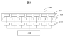
- 2 is a vertical cross-sectional view showing a schematic configuration of a wafer stage provided in the semiconductor etching system according to the embodiment;
- FIG. 1 is a plan view showing a schematic example of an arrangement of heater zones on the upper surface of a wafer stage in an embodiment.
- FIG. 1 is a flowchart showing a flow of operations in a computing device according to an embodiment.
- FIG. 2 is a diagram illustrating measurement points on a wafer surface.
- FIG. 13 is a schematic diagram for explaining the difference between the left and right CD and slope in a cross section.
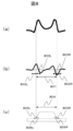
- 1 shows an example of an SEM image of a line pattern of a semiconductor device, a corresponding schematic cross-sectional view, and an example of a secondary electron signal waveform of the SEM.
- 1 shows an example of a secondary electron signal waveform, its first differential waveform, and the corresponding three-dimensional shape for calculating a feature amount that is a three-dimensional shape index.
- This is the value of the left-right difference in the CD, which is the first parameter, and the slope, which is the second parameter, calculated from the SEM image.
- the first parameter CD and the second parameter slope difference between the left and right sides are converted into a graph of temperature sensitivity.
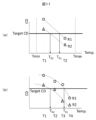
- 13 is a diagram for explaining a method of calculating the temperature of each electrode from a graph of temperature sensitivity to obtain uniform parameter values within a surface.
- FIG. 11 is a graph illustrating a state in which the temperature sensitivity is low.
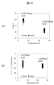
- 1 is a diagram showing the reduction in the variation in the CD value due to temperature control and the variation in the difference in the slope between the left and right sides.
- FIG. 13 is a diagram showing the reduction in the variation in the difference in slope between the left and right sides due to a change in the type of gas.
- FIG. 1 is a schematic diagram showing the configuration of a semiconductor etching system according to an embodiment of the present invention.
- This diagram shows the schematic overall configuration of a semiconductor etching system, and shows a semiconductor wafer processing device, such as an etching processing device, that processes semiconductor wafers to achieve a distribution of a specific physical quantity (for example, the shape or dimensions of a circuit pattern formed on the wafer surface) in the in-plane direction of the wafer.
- a specific physical quantity for example, the shape or dimensions of a circuit pattern formed on the wafer surface
- the semiconductor etching system of this embodiment includes an etching apparatus 103 having a wafer stage 105 in which a wafer 104 is placed and which has the function of variably adjusting the temperature distribution in the in-plane direction of the wafer 104, a measuring device 101 capable of measuring the distribution of a specific physical quantity in the wafer plane, a computer that calculates multiple parameter values including CD values obtained from the results of measuring a pattern formed on the surface of the wafer at multiple positions preset by the measuring device 101, and calculates the temperatures of multiple positions on the wafer or the stage supporting it using the parameter values, and a calculating device 102 having a mechanism for determining whether the parameter variations are within an acceptable range.
- the wafer stage 105 is provided with a plurality of heaters 201 for heating and a coolant flow path 204 for cooling under the surface on which the processing wafer 205 is placed.
- the temperature distribution in the in-plane direction of the wafer stage 105 is adjusted by adjusting the heat generation amount of the plurality of heaters 201 and the temperature of the coolant.
- the plurality of heaters 201 are installed in each area of the wafer stage 105, and the area can be divided into concentric circles as shown in FIG. 3(a) or into rectangles as shown in FIG. 3(b). These divided areas are called electrodes.
- 202 is a temperature regulator of the heater electrodes, and although not shown, it uses sensor values obtained from a plurality of temperature sensors installed on the heater electrodes to adjust the temperature of the stage top surface on which the wafer is placed to the wafer temperature calculated by the calculation device 102. This adjustment is controlled by the heater control unit 203.
- the coolant flow path 204 circulates between the coolant temperature controller connected via a pipe (not shown) and is adjusted to a temperature within a predetermined range in the coolant temperature controller.
- the coolant flow path 204 is installed below the heater 201, but it can also be installed above. Also, if the wafer temperature can be adjusted to the desired value using only the heater 201, it is not necessary to use a coolant.
- the calculation device 102 is a device that determines etching conditions that enable uniformity of the CD value and shape on the wafer before etching the production wafer, calculates the stage temperature for that purpose, and transmits it to the etching device 103.
- Figure 4 shows a flowchart performed by the calculation device. In this embodiment, an etching process is first performed using a wafer for calculation.
- the calculation wafer is a separate wafer that is pre-processed to obtain the parameters required for determining the above-mentioned processing conditions in order to obtain processing conditions that can bring the distribution of the CD value, shape, and dimensions of the film structure on the processed wafer in the in-plane direction within the desired range before etching a wafer (actual wafer) for manufacturing a semiconductor device (apparatus). It is a wafer on whose top surface there is pre-processed something that is the same as or can be considered to be the same as the film structure or pattern with multiple film layers including the film to be processed that is placed on the top surface of the actual wafer.
- step 400 data (processing recipe data) indicating the operation of the etching apparatus 103 shown in FIG. 1 including processing conditions such as the flow rate of the processing gas when the etching apparatus 103 processes a calculation wafer, the pressure in the processing chamber, the temperature of the wafer during processing and its distribution, i.e., the so-called processing recipe, is acquired by the computing device 102 via communication means and recorded in an internal storage device.
- step 401 an etching process is performed using the calculation wafer based on the obtained processing recipe data. In this embodiment, processing is performed on each of the multiple calculation wafers based on different temperature conditions.
- step 401 the temperature is changed for multiple calculation wafers, and processing is performed to calculate the temperature sensitivity of the desired pattern.
- etching processing is performed on each of two calculation wafers under conditions in which the wafer temperature during processing is set to 10°C and 50°C in the in-plane direction, and in particular, the temperature detected at each of multiple points on the wafer or wafer stage during processing is within a predetermined allowable range, and the CD value and its distribution are detected from these calculation wafers.
- step 402 the processed calculation wafers are measured.
- the CD value of the pattern is measured using a CD-SEM device that has been commonly used in the past. This is because it can be measured non-destructively and quickly.
- an image of the desired pattern at that location is acquired from the TopView using the CD-SEM device.
- the distribution of the measurement values obtained for multiple locations on the upper surface 501 of the calculation wafer in the in-plane direction can be calculated.
- the post-processing shapes formed at each of multiple predetermined inner locations of each of the dies 502 on which the device patterns of the upper surface 501 of the calculation wafer corresponding to each semiconductor device (chip) that will ultimately be cut out from the wafer are measured, and SEM images 503a, 503b, etc. are acquired.
- a CD-SEM image is a SEM image in which secondary electrons excited from atoms due to scattering of incident electrons within a sample are detected and displayed as shades of gray (brightness) for each pixel of the image. It represents the intensity of the detected secondary electron signal and contains information on the three-dimensional shape of the pattern.
- SEM images of multiple locations within the surface of a calculation wafer etched under conditions where the wafer temperature is 10°C, and multiple images of a calculation wafer etched under conditions of 50°C are acquired. Images were acquired of the patterns at designated locations within the area of each of the 110 dies 502 formed on the top surface 501 of each calculation wafer.
- the locations where the temperature of the wafer or wafer stage is detected are located below the area of each heater 201 whose output or heat amount is adjusted by the electrode control device so that the temperature outside the window is set to a desired value, and are located within the projection plane as viewed from above.
- the number of these locations is the same as or greater than the number of heaters 201. Even when the wafer temperature is set to a predetermined value in the in-plane direction as in steps 400 and 401, the output or heat amount of each heater 201 is adjusted so that the variation of each value falls within a desired range for the set of temperature values detected at multiple locations.
- each heater 201 having a rectangular area shown in Figure 3(b)
- the dimensions of each heater are made smaller than the dimensions of each die 502, and in this example, each heater 201 is adjusted based on the temperature detected at locations that are greater than the number of dies 502.
- step 403 shape parameters representing the three-dimensional shape are calculated from the acquired CD-SEM image.
- a parameter with high temperature sensitivity such as the CD value
- a parameter with low temperature sensitivity that is, a parameter with low correlation with the wafer temperature and high correlation with processing conditions other than temperature
- the second parameter such as a left-right difference in the slope of a cross section that has been experimentally confirmed to have low temperature sensitivity.
- parameters with low correlation with temperature also include parameters that have no correlation with temperature.
- the CD value represents the width of the cross section, and the difference in slope between the left and right sides is the difference in width between the left and right sides of the inclined surface of the pattern cross section,
- SADP Self-Aligned Double Patterning
- a feature value is a shape index that indicates the characteristics of the pattern shape, and refers to values such as peak and width obtained from the secondary electron signal waveform and its first and second derivative waveforms.
- Figure 8 shows an example of a feature value.
- (a) shows the secondary electron signal waveform,
- the value of the width of the waveform indicated by the arrow is called a feature value, and the shape of the pattern to be measured, such as the width (801, 804), footing (802, 805), and side angle of radiation (803, 806), is captured from the relationship between these multiple feature values.
- step 404 of the flow in FIG. 4 the electrode control temperature of the first parameter (CD value) is calculated.
- CD value the electrode control temperature of the first parameter
- FIG. 11 A method for calculating the temperature of each electrode to obtain a uniform parameter value within the surface from the temperature sensitivity graph will be described with reference to FIG. 11.
- the CD values obtained by measuring the calculation wafer etched at temperatures T1 and T2 with a CD-SEM are plotted only for electrode numbers R1 ( ⁇ ) and R2 ( ⁇ ), and the dashed lines are linear approximation lines for each electrode. From these linear approximation lines, the temperature of each electrode is calculated to obtain the CD value of the target shown in the graph.
- the temperature T R1 of electrode R1 is obtained from the intersection of the linear approximation line of electrode R1 with the target
- the temperature T R2 of electrode R2 is obtained from the intersection of the linear approximation line of electrode R2 with the linear approximation line of electrode R2.
- the electrode is a part of the etching device, and there is a range of temperatures that can be controlled.
- the minimum temperature is Tmin and the maximum temperature is Tmax
- the calculation wafer processing temperatures T1 and T2 are usually within the range of Tmin and Tmax.
- the calculated temperatures T R1 and T R2 are also within the range of Tmin and Tmax.
- the electrode temperature cannot be realized.
- such a small gradient means that even if the temperature is changed between Tmin and Tmax, the change in the parameter value is small, and the temperature sensitivity is small.
- step 405 is a process for determining whether the variation in the second parameter with low temperature sensitivity (left-right difference in slope) is within a predetermined tolerance. If the variation is within the specified value (Yes), it is determined that the variation in both the first parameter (CD value) and the second parameter calculated in step 404 for the shape after processing by the etching process based on the initial processing recipe data including the temperature conditions is within a predetermined tolerance required for the semiconductor device or its manufacture, and the process proceeds to the next step 406, a process for processing actual wafers for manufacturing semiconductor devices.
- the initial CD variation ⁇ CD (10 deg) and ⁇ CD (50 deg) obtained by processing the calculation wafer at the temperature conditions of 10° C. and 50° C. included in the processing recipe data as the initial values are calculated, and these values are compared with the upper limit of the allowable range of the CD variation. If it is determined that the variation value is outside the allowable range with the upper limit value as the threshold, the calculation device calculates the temperature values and their distribution to be set at the multiple locations where the temperature is detected in order to bring the CD variation into the allowable range.
- the set of temperature settings at the multiple locations during processing as such a processing condition is set as a temperature group, and the heater 201 is adjusted to these temperatures under the processing conditions using the temperature group T3 group corrected to improve the CD variation, and the variation ⁇ CD (T3 group) resulting from processing the calculation wafer is as shown in FIG. 13(a).
- ⁇ S 10 deg
- ⁇ S 50 deg
- step 407 is performed again and the flow is restarted. In this way, the loop of steps 400 to 405 or steps 407 and 408 is repeated until the variation is determined to be within the specified value in step 405.
- processing is performed using a processing recipe in which the processing conditions based on the first parameter have been modified based on the determination using the second parameter.
- step 404 is performed after step 403, in which parameters including the first and second ones of the calculation wafer are calculated, and before step 405, which is a judgment process using the second parameter, but if the judgment in step 405 is that the value is outside the specified value (No), it may be performed again in the processes after step 400 before correcting the processing recipe data before the parameter is calculated.
- the difference in slope between the left and right sides was selected as the second parameter with low temperature sensitivity, but experiments have shown that sub-trench and mask erosion also have low temperature sensitivity, and that the in-plane uniformity can be improved by reconsidering the wafer bias rather than the temperature, so the same applies if these are selected as the second parameter.
- the temperature sensitivity of the parameter can be confirmed as shown in Figures 11 and 12 of this embodiment.
- the temperature sensitivity of a feature calculated from an SEM image the temperature sensitivity of a three-dimensional shape parameter that has a strong correlation with that feature can be determined. Since multiple feature amounts corresponding to three-dimensional shape parameters are calculated from an SEM image, the temperature sensitivity of each feature amount can be confirmed, and a feature amount with a high temperature sensitivity can be selected as a first parameter, and a feature amount with a low temperature sensitivity can be selected as a second parameter.
- step 403 or step 404 may be selected instead of step 400 as the process for returning from step 408 in the flowchart shown in FIG. 4.
- the first and second parameters were both widths (nm) and had the same dimensions, so they could be compared as is, but the multiple feature quantities corresponding to the three-dimensional shape parameters each have different dimensions. In this case, it is necessary to standardize the data using data from a reference die so that they can be compared in the same dimensions.
- CD values and three-dimensional shape are assumed as physical quantities, electrical characteristics are also possible. In that case, an electrical characteristic evaluation device is used as the measurement device rather than a CD-SEM.
- 101 Measuring device, 102: Calculating device, 103: Etching device, 104: Wafer, 105: Wafer stage, 201: Heater, 202: Temperature regulator, 203: Heater control unit, 204: Coolant flow path, 205: Processing wafer, 501: Calculation wafer top surface, 502: Die, 503: SEM image.
Landscapes
- General Health & Medical Sciences (AREA)
- General Physics & Mathematics (AREA)
- Life Sciences & Earth Sciences (AREA)
- Chemical & Material Sciences (AREA)
- Analytical Chemistry (AREA)
- Biochemistry (AREA)
- Immunology (AREA)
- Physics & Mathematics (AREA)
- Health & Medical Sciences (AREA)
- Pathology (AREA)
- Drying Of Semiconductors (AREA)
- Automation & Control Theory (AREA)
- Engineering & Computer Science (AREA)
- Testing Or Measuring Of Semiconductors Or The Like (AREA)
Abstract
Description
Claims (10)
- ウエハをエッチングするエッチング装置と、前記エッチング装置によりエッチングされた前記ウエハの表面上に形成されたパターンを測定する測定装置と、前記エッチング装置にエッチング条件を提供する計算装置とを備え、
前記計算装置が、前記測定装置からの前記パターンの測定結果に基づいてエッチング条件のうちの温度条件と相関の高い第1のパラメータと相関の低い第2のパラメータを算出し、算出した前記第1のパラメータに基づいて前記第1のパラメータが許容範囲内となる温度条件を算出し、算出した前記第2のパラメータが許容範囲内かどうかを判定し、
算出した前記第2のパラメータが許容範囲外の場合に、温度条件以外の条件を変更したエッチング条件を提供し、算出した前記第2のパラメータが許容範囲内の場合に、温度条件を算出した温度条件に変更したエッチング条件を提供することを特徴とするエッチングシステム。 - 前記第1のパラメータが前記パターンのCD値であり、前記第2のパラメータが前記パターンの断面の斜面の左右の幅の差であることを特徴とする請求項1に記載のエッチングシステム。
- 前記測定装置がCD-SEM測定装置であり、前記パターンのTopViewからのSEM画像を取得することを特徴とする請求項2に記載のエッチングシステム。
- 前記SEM画像から前記パターンのCD値と断面の斜面の左右の幅の差を算出することを特徴とする請求項3に記載のエッチングシステム。
- 算出した前記パターンの断面の斜面の左右の幅の差が許容範囲外の場合に、ガスを変更したエッチング条件を前記エッチング装置に提供することを特徴とする請求項4に記載のエッチングシステム。
- ウエハをエッチングするエッチング装置と、前記エッチング装置によりエッチングされたウエハの表面上に形成されたパターンを測定する測定装置と、前記エッチング装置にエッチング条件を提供する計算装置とを用いたエッチング方法において、
提供されたエッチング条件でウエハをエッチングする第1のステップと、
前記第1のステップでエッチングされたウエハの表面上に形成されたパターンを測定する第2のステップと、
前記第2のステップの測定結果に基づいてエッチング条件のうちの温度条件と相関の高い第1のパラメータと相関の低い第2のパラメータを算出する第3のステップと、
前記第3のステップで算出した前記第1のパラメータに基づいて前記第1のパラメータが許容範囲内となる温度条件を算出する第4のステップと、
前記第3のステップで算出した前記第2のパラメータが許容範囲内かどうかを判定する第5のステップと、
前記第5のステップの判定が許容範囲外の場合に、温度条件以外の条件を変更したエッチング条件を前記エッチング装置に提供する第6のステップと、
前記第5のステップの判定が許容範囲内の場合に、前記第4のステップで算出した温度条件に変更したエッチング条件を前記エッチング装置に提供する第7のステップを有し、
前記第5のステップの判定が許容範囲外となった場合、前記第5のステップの判定が許容範囲内となるまで前記第1乃至第6のステップを繰り返すことを特徴とするエッチング方法。 - 前記第1のパラメータが前記パターンのCD値であり、前記第2のパラメータが前記パターンの断面の斜面の左右の幅の差であることを特徴とする請求項6に記載のエッチング方法。
- 前記測定装置がCD-SEM測定装置であり、前記第2のステップにおいて前記パターンのTopViewからのSEM画像を取得することを特徴とする請求項7に記載のエッチング方法。
- 前記第3のステップにおいて前記SEM画像から前記パターンのCD値と断面の斜面の左右の幅の差を算出することを特徴とする請求項8に記載のエッチング方法。
- 前記第6のステップにおいてガスを変更したエッチング条件を前記エッチング装置に提供することを特徴とする請求項9に記載のエッチング方法。
Priority Applications (5)
| Application Number | Priority Date | Filing Date | Title |
|---|---|---|---|
| JP2024543555A JP7724977B2 (ja) | 2023-07-10 | 2023-07-10 | エッチングシステム及びエッチング方法 |
| PCT/JP2023/025382 WO2025013151A1 (ja) | 2023-07-10 | 2023-07-10 | エッチングシステム及びエッチング方法 |
| CN202380020746.6A CN119604967A (zh) | 2023-07-10 | 2023-07-10 | 蚀刻系统以及蚀刻方法 |
| KR1020247024837A KR20250009953A (ko) | 2023-07-10 | 2023-07-10 | 에칭 시스템 및 에칭 방법 |
| TW113125600A TWI881879B (zh) | 2023-07-10 | 2024-07-09 | 蝕刻系統及蝕刻方法 |
Applications Claiming Priority (1)
| Application Number | Priority Date | Filing Date | Title |
|---|---|---|---|
| PCT/JP2023/025382 WO2025013151A1 (ja) | 2023-07-10 | 2023-07-10 | エッチングシステム及びエッチング方法 |
Publications (1)
| Publication Number | Publication Date |
|---|---|
| WO2025013151A1 true WO2025013151A1 (ja) | 2025-01-16 |
Family
ID=94214798
Family Applications (1)
| Application Number | Title | Priority Date | Filing Date |
|---|---|---|---|
| PCT/JP2023/025382 Ceased WO2025013151A1 (ja) | 2023-07-10 | 2023-07-10 | エッチングシステム及びエッチング方法 |
Country Status (5)
| Country | Link |
|---|---|
| JP (1) | JP7724977B2 (ja) |
| KR (1) | KR20250009953A (ja) |
| CN (1) | CN119604967A (ja) |
| TW (1) | TWI881879B (ja) |
| WO (1) | WO2025013151A1 (ja) |
Cited By (1)
| Publication number | Priority date | Publication date | Assignee | Title |
|---|---|---|---|---|
| CN119725137A (zh) * | 2025-02-26 | 2025-03-28 | 合肥晶合集成电路股份有限公司 | 晶圆刻蚀系统的控制方法、装置、计算机设备和系统 |
Citations (3)
| Publication number | Priority date | Publication date | Assignee | Title |
|---|---|---|---|---|
| JP2012204806A (ja) * | 2011-03-28 | 2012-10-22 | Tokyo Electron Ltd | 判定方法、制御方法、判定装置、パターン形成システム及びプログラム |
| JP2018117115A (ja) * | 2017-01-19 | 2018-07-26 | 東京エレクトロン株式会社 | 基板処理装置、温度制御方法及び温度制御プログラム |
| US20190172718A1 (en) * | 2017-12-05 | 2019-06-06 | Asm Ip Holding B.V. | Method for forming vertical spacers for spacer-defined patterning |
Family Cites Families (6)
| Publication number | Priority date | Publication date | Assignee | Title |
|---|---|---|---|---|
| JP3799314B2 (ja) | 2002-09-27 | 2006-07-19 | 株式会社日立ハイテクノロジーズ | エッチング処理装置およびエッチング処理方法 |
| US6770852B1 (en) | 2003-02-27 | 2004-08-03 | Lam Research Corporation | Critical dimension variation compensation across a wafer by means of local wafer temperature control |
| JP2006216822A (ja) | 2005-02-04 | 2006-08-17 | Hitachi High-Technologies Corp | ウェハ処理装置およびウェハ処理方法 |
| JP2007035777A (ja) | 2005-07-25 | 2007-02-08 | Oki Electric Ind Co Ltd | 半導体装置の製造方法及び半導体製造装置 |
| JP5779482B2 (ja) * | 2011-11-15 | 2015-09-16 | 株式会社日立ハイテクノロジーズ | プラズマ処理装置およびプラズマ処理方法 |
| JP6591377B2 (ja) | 2015-10-08 | 2019-10-16 | 株式会社ニューフレアテクノロジー | 気相成長速度測定装置、気相成長装置および成長速度検出方法 |
-
2023
- 2023-07-10 CN CN202380020746.6A patent/CN119604967A/zh active Pending
- 2023-07-10 KR KR1020247024837A patent/KR20250009953A/ko active Pending
- 2023-07-10 WO PCT/JP2023/025382 patent/WO2025013151A1/ja not_active Ceased
- 2023-07-10 JP JP2024543555A patent/JP7724977B2/ja active Active
-
2024
- 2024-07-09 TW TW113125600A patent/TWI881879B/zh active
Patent Citations (3)
| Publication number | Priority date | Publication date | Assignee | Title |
|---|---|---|---|---|
| JP2012204806A (ja) * | 2011-03-28 | 2012-10-22 | Tokyo Electron Ltd | 判定方法、制御方法、判定装置、パターン形成システム及びプログラム |
| JP2018117115A (ja) * | 2017-01-19 | 2018-07-26 | 東京エレクトロン株式会社 | 基板処理装置、温度制御方法及び温度制御プログラム |
| US20190172718A1 (en) * | 2017-12-05 | 2019-06-06 | Asm Ip Holding B.V. | Method for forming vertical spacers for spacer-defined patterning |
Cited By (1)
| Publication number | Priority date | Publication date | Assignee | Title |
|---|---|---|---|---|
| CN119725137A (zh) * | 2025-02-26 | 2025-03-28 | 合肥晶合集成电路股份有限公司 | 晶圆刻蚀系统的控制方法、装置、计算机设备和系统 |
Also Published As
| Publication number | Publication date |
|---|---|
| KR20250009953A (ko) | 2025-01-20 |
| JP7724977B2 (ja) | 2025-08-18 |
| TW202503891A (zh) | 2025-01-16 |
| TWI881879B (zh) | 2025-04-21 |
| CN119604967A (zh) | 2025-03-11 |
| JPWO2025013151A1 (ja) | 2025-01-16 |
Similar Documents
| Publication | Publication Date | Title |
|---|---|---|
| US6913861B2 (en) | Method of observing exposure condition for exposing semiconductor device and its apparatus and method of manufacturing semiconductor device | |
| KR100804284B1 (ko) | 산란 측정을 이용하여 피드백 및 피드-포워드 제어를 수행하기 위한 방법 및 그 장치와, 그리고 상기 방법을 수행하기 위한 명령어들이 코드화된 컴퓨터 판독가능 프로그램 저장 매체 | |
| TWI572993B (zh) | 用於判定一微影製程之製程窗之方法、相關設備及一電腦程式 | |
| US6486492B1 (en) | Integrated critical dimension control for semiconductor device manufacturing | |
| EP3444673A1 (en) | Method of adapting feed-forward parameters | |
| JP4065817B2 (ja) | 露光プロセスモニタ方法 | |
| TW201633008A (zh) | 微影方法與微影裝置 | |
| KR102379329B1 (ko) | 피쳐의 위치를 결정하는 방법 | |
| JP2005286095A (ja) | 露光プロセスモニタ方法及びその装置 | |
| US7369697B2 (en) | Process variable of interest monitoring and control | |
| JP7724977B2 (ja) | エッチングシステム及びエッチング方法 | |
| KR101204667B1 (ko) | 위상반전마스크의 시디 보정방법 및 그 제조방법 | |
| JP5286337B2 (ja) | 半導体製造装置の管理装置、及びコンピュータプログラム | |
| JP5134804B2 (ja) | 走査電子顕微鏡および走査電子顕微鏡像の歪み校正 | |
| TW201721307A (zh) | 控制微影設備之方法、微影設備及器件製造方法 | |
| KR102183619B1 (ko) | 모니터링 방법 및 디바이스의 제조 방법 | |
| KR102454701B1 (ko) | 디바이스 제조 방법 | |
| US8373845B2 (en) | Exposure control apparatus, manufacturing method of semiconductor device, and exposure apparatus | |
| US7230239B2 (en) | Apparatus for inspecting three dimensional shape of a specimen and method of watching an etching process using the same | |
| CN117234039B (zh) | 晶圆套刻对象的灰度值变化测量方法及系统 | |
| JP4383817B2 (ja) | 電子ビーム描画における近接効果補正の検証方法 | |
| JP2008205393A (ja) | アライメントマークの位置検出の条件を決定する方法、露光装置及びデバイスの製造方法 | |
| TW201835677A (zh) | 判定圖案化製程之校正之方法、元件製造方法、用於微影裝置之控制系統及微影裝置 | |
| US10438771B2 (en) | Measurement device, calibration method of measurement device, and calibration member | |
| JP2025156800A (ja) | 半導体パターン評価方法、半導体製造プロセス管理システム、半導体パターン評価システム |
Legal Events
| Date | Code | Title | Description |
|---|---|---|---|
| WWE | Wipo information: entry into national phase |
Ref document number: 2024543555 Country of ref document: JP |
|
| WWE | Wipo information: entry into national phase |
Ref document number: 202380020746.6 Country of ref document: CN |
|
| WWE | Wipo information: entry into national phase |
Ref document number: 18845688 Country of ref document: US |
|
| 121 | Ep: the epo has been informed by wipo that ep was designated in this application |
Ref document number: 23945031 Country of ref document: EP Kind code of ref document: A1 |
|
| WWP | Wipo information: published in national office |
Ref document number: 202380020746.6 Country of ref document: CN |
|
| NENP | Non-entry into the national phase |
Ref country code: DE |