WO2025009428A1 - 光学系、画像投写装置および撮像装置 - Google Patents
光学系、画像投写装置および撮像装置 Download PDFInfo
- Publication number
- WO2025009428A1 WO2025009428A1 PCT/JP2024/022800 JP2024022800W WO2025009428A1 WO 2025009428 A1 WO2025009428 A1 WO 2025009428A1 JP 2024022800 W JP2024022800 W JP 2024022800W WO 2025009428 A1 WO2025009428 A1 WO 2025009428A1
- Authority
- WO
- WIPO (PCT)
- Prior art keywords
- optical system
- optical
- sub
- transmitting surface
- transmitting
- Prior art date
- Legal status (The legal status is an assumption and is not a legal conclusion. Google has not performed a legal analysis and makes no representation as to the accuracy of the status listed.)
- Ceased
Links
Images





Classifications
-
- G—PHYSICS
- G03—PHOTOGRAPHY; CINEMATOGRAPHY; ANALOGOUS TECHNIQUES USING WAVES OTHER THAN OPTICAL WAVES; ELECTROGRAPHY; HOLOGRAPHY
- G03B—APPARATUS OR ARRANGEMENTS FOR TAKING PHOTOGRAPHS OR FOR PROJECTING OR VIEWING THEM; APPARATUS OR ARRANGEMENTS EMPLOYING ANALOGOUS TECHNIQUES USING WAVES OTHER THAN OPTICAL WAVES; ACCESSORIES THEREFOR
- G03B21/00—Projectors or projection-type viewers; Accessories therefor
- G03B21/54—Accessories
- G03B21/56—Projection screens
-
- G—PHYSICS
- G02—OPTICS
- G02B—OPTICAL ELEMENTS, SYSTEMS OR APPARATUS
- G02B13/00—Optical objectives specially designed for the purposes specified below
- G02B13/001—Miniaturised objectives for electronic devices, e.g. portable telephones, webcams, PDAs, small digital cameras
- G02B13/0015—Miniaturised objectives for electronic devices, e.g. portable telephones, webcams, PDAs, small digital cameras characterised by the lens design
- G02B13/002—Miniaturised objectives for electronic devices, e.g. portable telephones, webcams, PDAs, small digital cameras characterised by the lens design having at least one aspherical surface
- G02B13/0045—Miniaturised objectives for electronic devices, e.g. portable telephones, webcams, PDAs, small digital cameras characterised by the lens design having at least one aspherical surface having five or more lenses
-
- G—PHYSICS
- G02—OPTICS
- G02B—OPTICAL ELEMENTS, SYSTEMS OR APPARATUS
- G02B13/00—Optical objectives specially designed for the purposes specified below
- G02B13/16—Optical objectives specially designed for the purposes specified below for use in conjunction with image converters or intensifiers, or for use with projectors, e.g. objectives for projection TV
-
- G—PHYSICS
- G02—OPTICS
- G02B—OPTICAL ELEMENTS, SYSTEMS OR APPARATUS
- G02B13/00—Optical objectives specially designed for the purposes specified below
- G02B13/18—Optical objectives specially designed for the purposes specified below with lenses having one or more non-spherical faces, e.g. for reducing geometrical aberration
-
- G—PHYSICS
- G02—OPTICS
- G02B—OPTICAL ELEMENTS, SYSTEMS OR APPARATUS
- G02B17/00—Systems with reflecting surfaces, with or without refracting elements
- G02B17/08—Catadioptric systems
-
- G—PHYSICS
- G02—OPTICS
- G02B—OPTICAL ELEMENTS, SYSTEMS OR APPARATUS
- G02B17/00—Systems with reflecting surfaces, with or without refracting elements
- G02B17/08—Catadioptric systems
- G02B17/0804—Catadioptric systems using two curved mirrors
- G02B17/0812—Catadioptric systems using two curved mirrors off-axis or unobscured systems in which all of the mirrors share a common axis of rotational symmetry
-
- G—PHYSICS
- G03—PHOTOGRAPHY; CINEMATOGRAPHY; ANALOGOUS TECHNIQUES USING WAVES OTHER THAN OPTICAL WAVES; ELECTROGRAPHY; HOLOGRAPHY
- G03B—APPARATUS OR ARRANGEMENTS FOR TAKING PHOTOGRAPHS OR FOR PROJECTING OR VIEWING THEM; APPARATUS OR ARRANGEMENTS EMPLOYING ANALOGOUS TECHNIQUES USING WAVES OTHER THAN OPTICAL WAVES; ACCESSORIES THEREFOR
- G03B21/00—Projectors or projection-type viewers; Accessories therefor
-
- G—PHYSICS
- G03—PHOTOGRAPHY; CINEMATOGRAPHY; ANALOGOUS TECHNIQUES USING WAVES OTHER THAN OPTICAL WAVES; ELECTROGRAPHY; HOLOGRAPHY
- G03B—APPARATUS OR ARRANGEMENTS FOR TAKING PHOTOGRAPHS OR FOR PROJECTING OR VIEWING THEM; APPARATUS OR ARRANGEMENTS EMPLOYING ANALOGOUS TECHNIQUES USING WAVES OTHER THAN OPTICAL WAVES; ACCESSORIES THEREFOR
- G03B21/00—Projectors or projection-type viewers; Accessories therefor
- G03B21/14—Details
- G03B21/20—Lamp housings
- G03B21/208—Homogenising, shaping of the illumination light
-
- G—PHYSICS
- G03—PHOTOGRAPHY; CINEMATOGRAPHY; ANALOGOUS TECHNIQUES USING WAVES OTHER THAN OPTICAL WAVES; ELECTROGRAPHY; HOLOGRAPHY
- G03B—APPARATUS OR ARRANGEMENTS FOR TAKING PHOTOGRAPHS OR FOR PROJECTING OR VIEWING THEM; APPARATUS OR ARRANGEMENTS EMPLOYING ANALOGOUS TECHNIQUES USING WAVES OTHER THAN OPTICAL WAVES; ACCESSORIES THEREFOR
- G03B21/00—Projectors or projection-type viewers; Accessories therefor
- G03B21/14—Details
- G03B21/28—Reflectors in projection beam
Definitions
- This disclosure relates to an optical system that has an intermediate imaging position inside. This disclosure also relates to an image projection device and an imaging device that use such an optical system.
- Patent Document 1 discloses a projection optical system and an image projection device that use a cemented lens or a D-cut lens.
- the D-cut lens is a single optical element that does not have a boundary surface, and the entrance surface 40A and the exit surface 40D share the same optical surface.
- the entrance surface 40A and the exit surface 40D cannot be separated.
- the exit surface 40D must be convex, which means that the entrance surface 40A also becomes convex. If the entrance surface 40A becomes convex, the effective diameter of the refractive optical system becomes large in order to obtain the intermediate image Im1 at a specified position. As a result, the overall length of the optical system becomes longer, and the image projection device also becomes larger.
- This disclosure provides an optical system that enables short-focus, large-screen projection or imaging in an oblique direction. This disclosure also provides an image projection device and imaging device that use such an optical system.
- One aspect of the present disclosure is an optical system having a reduction conjugate point on a reduction side and a magnification conjugate point on a magnification side, and having intermediate image positions therein that are conjugates to the reduction conjugate point and the magnification conjugate point, a first sub-optical system including a plurality of lenses that are rotationally symmetric with respect to an optical axis and a stop between the plurality of lenses; a second sub-optical system arranged on the enlargement side of the first sub-optical system and having a plurality of optical surfaces; a magnification conjugate plane including the magnification conjugate point is disposed on the reduction side as viewed from the second sub-optical system, the plurality of optical surfaces include a first transmitting surface located closest to the first sub-optical system on an optical path between the first sub-optical system and the magnification conjugate point, a second transmitting surface located closest to the magnification conjugate point, a first reflecting surface located closest to the first transmitting surface on the optical path between the
- An image projection device includes the above optical system and an image forming element that generates an image to be projected onto a screen via the optical system.
- An imaging device includes the above optical system and an imaging element that receives an optical image formed by the optical system and converts it into an electrical image signal.
- the optical system disclosed herein allows for a high degree of freedom in optical design, making it possible to realize an optical system that is advantageous for achieving a wide angle.
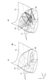
- Fig. 2A is a perspective view showing the three-dimensional shape of each optical surface of the prism PM, and Fig. 2B shows a part of a light ray traveling inside the prism PM.
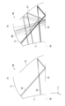
- Fig. 3A is a cross-sectional view of the prism PM along the YZ plane, and Fig. 3B shows a part of a light ray traveling inside the prism PM.
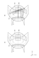
- Fig. 4A is a top view of the prism PM as viewed from the Y direction, and Fig. 4B shows a part of a light beam traveling inside the prism PM.
- Fig. 3A is a cross-sectional view of the prism PM along the YZ plane
- Fig. 3B shows a part of a light ray traveling inside the prism PM.
- Fig. 4A is a top view of the prism PM as viewed from the Y direction
- Fig. 4B shows a part of a light beam traveling inside the prism PM.
- 5A is a cross-sectional view showing the light beam closest to the optical axis OA inside the prism PM and its chief ray PR
- Fig. 5B is a cross-sectional view showing a Y-direction intermediate image IMy on the YZ plane.
- 6A is a YZ cross-sectional view for explaining the definition of the angle ⁇ a of the direction in which the principal ray PR is reflected by the second reflecting surface R2
- FIG. 6B is a YZ cross-sectional view for explaining the definition of the angle ⁇ b of the direction in which the principal ray PR advances outside the prism PM.
- Fig. 15(A) is a layout diagram showing an example of obliquely upward rear projection onto a wall screen SR.
- Fig. 15(B) is a layout diagram showing an example of obliquely downward rear projection onto a wall screen SR.
- FIG. 15(C) is a layout diagram showing an example of obliquely upward rear projection onto a ceiling screen SR.
- Fig. 15(D) is a layout diagram showing an example of obliquely downward rear projection onto a floor screen SR.
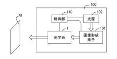
- FIG. 1 is a block diagram illustrating an example of an image projection device according to the present disclosure.
- FIG. 1 is a block diagram illustrating an example of an imaging device according to the present disclosure.
- the optical system is used in a projector (one example of an image projection device) that projects onto a screen the image light of an original image SA, which is formed by spatially modulating incident light using an image forming element such as a liquid crystal or a DMD (digital micromirror device) based on an image signal. That is, the optical system according to the present disclosure can be used to enlarge and project onto a screen an original image SA on an image forming element arranged on the reduction side by arranging a screen (not shown) on an extension of the enlargement side.
- the projection surface is not limited to a screen. Projection surfaces also include walls, ceilings, floors, and windows inside homes and stores, or vehicles and aircraft used for mobile transportation.
- the optical system disclosed herein can also be used to collect light emitted from an object located on the extension of the magnification side and form an optical image of the object on the imaging surface of an imaging element located on the reduction side.
- Example 1 Fig. 1 is a layout diagram showing an optical system 1 according to Example 1.
- the optical system 1 includes a first sub-optical system including a plurality of lens elements and an aperture stop ST, and a second sub-optical system having a plurality of optical surfaces.
- a reduction conjugate point which is an imaging position on the reduction side
- a magnification conjugate point which is an imaging position on the magnification side
- the second sub-optical system is provided on the magnification side of the first sub-optical system.
- optical system 1 there is an intermediate imaging position that is conjugate to the reduction conjugate point and the enlargement conjugate point.
- this intermediate imaging position both the Y-direction intermediate image IMy and the X-direction intermediate image IMx exist within the second sub-optical system.
- the Y-direction intermediate image IMy is shown in Figure 1, but the X-direction intermediate image IMx is not shown.
- the first sub-optical system includes, from the reduction side to the enlargement side, an optical element PA and lens elements L1 to L10.
- the optical element PA represents an optical element such as a TIR (total internal reflection) prism, a prism for color separation and color synthesis, an optical filter, parallel plate glass, a quartz low-pass filter, and an infrared cut filter.
- a reduction conjugate point is set at a position a predetermined distance from the reduction side end face of the optical element PA, and the original image SA is placed here.
- the optical element PA has two parallel, flat transmitting surfaces (surfaces 1 and 2).
- Surfaces 1 and 2 For the surface numbers, refer to the numerical examples described later.
- Lens element L1 has a biconvex shape (surfaces 3 and 4).
- Lens element L2 has a biconcave shape (surfaces 5 and 6).
- Lens element L3 has a biconvex shape (surfaces 7 and 8).
- Lens element L4 has a negative meniscus shape with the convex surface facing the reduction side (surfaces 9 and 10).
- Lens element L5 has a biconvex shape (surfaces 11 and 12).
- Lens element L6 has a negative meniscus shape with the convex surface facing the reduction side (surfaces 13 and 14).
- Lens element L7 has a biconvex shape (surfaces 16 and 17).
- Lens element L8 has a positive meniscus shape with the convex surface facing the reduction side (surfaces 18 and 19).
- Lens element L9 has a biconcave shape (surfaces 20 and 21).
- Lens element L10 has a biconcave shape (surfaces 22 and 23).
- These lens elements L1 to L10 are rotationally symmetric lenses that have a surface shape that is rotationally symmetric around the optical axis OA of the first sub-optical system, and if necessary, portions through which light rays do not pass may be removed.
- the second sub-optical system includes a prism PM formed of a transparent medium, such as glass or synthetic resin.
- the prism PM has a plurality of optical surfaces.
- the plurality of optical surfaces include a first transmitting surface T1 located closest to the first sub-optical system on the optical path between the first sub-optical system and the magnification conjugate point, a second transmitting surface T2 located closest to the magnification conjugate point, and a first reflecting surface R1 located closest to the first transmitting surface T1 and a second reflecting surface R2 located closest to the second transmitting surface T2 on the optical path between the first transmitting surface T1 and the second transmitting surface T2.
- the first transmitting surface T1 has a free-form surface shape with a convex surface facing the magnification side (surface 24).
- the first reflecting surface R1 has a free-form surface shape with a concave surface facing in the direction in which the light ray incident on the first reflecting surface R1 is reflected (surface 25).
- the second reflecting surface R2 has a free-form surface shape with a convex surface facing in the direction in which the light ray incident on the second reflecting surface R2 is reflected (surface 26).
- the second transmitting surface T2 has a free-form shape with a convex surface facing the magnification side (surface 27).
- the aperture stop ST defines the range through which the light beam passes through the optical system 1, and is positioned between the reduction conjugate point and the intermediate image position described above.
- the aperture stop ST is located between lens elements L6 and L7 (surface 15).
- FIG. 2(A) is a perspective view showing the three-dimensional shape of each optical surface of the prism PM
- FIG. 2(B) shows some of the light rays traveling inside the prism PM.
- the first transmitting surface T1 is curved so that it faces concave in the -Z direction
- the second transmitting surface T2 has a shape like a partial dome that covers the other optical surfaces from above
- the first reflecting surface R1 faces the first transmitting surface T1
- the second reflecting surface R2 faces the second transmitting surface T2.
- FIG. 3(A) is a cross-sectional view of the prism PM along the YZ plane
- FIG. 3(B) shows some of the light rays traveling inside the prism PM.
- FIG. 4(A) is a top view of the prism PM as seen from the Y direction
- FIG. 4(B) shows some of the light rays traveling inside the prism PM.
- Figure 5 (A) is a YZ cross-sectional view showing the light beam closest to the optical axis OA inside the prism PM and its chief ray PR.
- Figure 5 (B) is a YZ cross-sectional view showing the Y-direction intermediate image IMy on the YZ plane.
- Figure 6 (A) is a YZ cross-sectional view explaining the definition of the angle ⁇ a of the direction in which the chief ray PR is reflected by the second reflecting surface R2.
- Figure 6 (B) is a YZ cross-sectional view explaining the definition of the angle ⁇ b of the direction in which the chief ray PR travels outside the prism PM. Details will be described later.
- FIG. 7 and 8 are lateral aberration diagrams of the optical system 1 according to Example 1.
- the solid line indicates a wavelength of 550 nm
- the dashed line indicates a wavelength of 610 nm
- the dashed line indicates a wavelength of 455 nm. From these graphs, it can be seen that the optical system 1 according to Example 1 exhibits excellent optical performance.
- Example 2 Fig. 9 is a layout diagram showing an optical system 1 according to Example 2.
- This optical system 1 has a configuration similar to that of Example 1, and a description that overlaps with Example 1 will be omitted.
- the optical system 1 includes a first sub-optical system including a plurality of lens elements and an aperture stop ST, and a second sub-optical system having a plurality of optical surfaces.
- a reduction conjugate point which is an imaging position on the reduction side
- a magnification conjugate point which is an imaging position on the magnification side
- the second sub-optical system is provided on the magnification side of the first sub-optical system.
- optical system 1 there is an intermediate imaging position that is conjugate to the reduction conjugate point and the enlargement conjugate point.
- this intermediate imaging position both the Y-direction intermediate image IMy and the X-direction intermediate image IMx exist within the second sub-optical system.
- the Y-direction intermediate image IMy is shown in Figure 9, but the X-direction intermediate image IMx is not shown.
- the first sub-optical system includes, from the reduction side to the enlargement side, an optical element PA and lens elements L1 to L11.
- a reduction conjugate point is set at a position a predetermined distance from the reduction side end face of the optical element PA, and the original image SA is placed here.
- the optical element PA has two parallel, flat transmitting surfaces (surfaces 1 and 2).
- Surfaces 1 and 2 For the surface numbers, refer to the numerical examples described later.
- Lens element L1 has a biconvex shape (surfaces 3 and 4).
- Lens element L2 has a negative meniscus shape with a convex surface facing the reduction side (surfaces 5 and 6).
- Lens element L3 has a biconvex shape (surfaces 7 and 8).
- Lens element L4 has a negative meniscus shape with a convex surface facing the reduction side (surfaces 9 and 10).
- Lens element L5 has a biconvex shape (surfaces 11 and 12).
- Lens element L6 has a negative meniscus shape with a convex surface facing the reduction side (surfaces 13 and 14).
- Lens element L7 has a biconvex shape (surfaces 16 and 17).
- Lens element L8 has a positive meniscus shape with a convex surface facing the reduction side (surfaces 18 and 19).
- Lens element L9 has a negative meniscus shape with a convex surface facing the enlargement side (surfaces 20 and 21).
- Lens element L10 has a biconcave shape (surfaces 22, 23).
- Lens element L11 has a negative meniscus shape with a convex surface facing the magnification side (surfaces 24, 25).
- These lens elements L1 to L11 are rotationally symmetric lenses that have surface shapes that are rotationally symmetric around the optical axis OA of the first sub-optical system, and portions through which light rays do not pass may be removed if necessary.
- the second sub-optical system includes a prism PM formed of a transparent medium, such as glass or synthetic resin.
- the prism PM has a plurality of optical surfaces.
- the plurality of optical surfaces include a first transmitting surface T1 located closest to the first sub-optical system on the optical path between the first sub-optical system and the magnification conjugate point, a second transmitting surface T2 located closest to the magnification conjugate point, and a first reflecting surface R1 located closest to the first transmitting surface T1 and a second reflecting surface R2 located closest to the second transmitting surface T2 on the optical path between the first transmitting surface T1 and the second transmitting surface T2.
- the first transmitting surface T1 has a free-form surface shape with a convex surface facing the magnification side (surface 26).
- the first reflecting surface R1 has a free-form surface shape with a concave surface facing in the direction in which the light ray incident on the first reflecting surface R1 is reflected (surface 27).
- the second reflecting surface R2 has a free-form surface shape with a convex surface facing in the direction in which the light ray incident on the second reflecting surface R2 is reflected (surface 28).
- the second transmitting surface T2 has a free-form shape with a convex surface facing the magnification side (surface 29).
- FIGS. 10 and 11 are lateral aberration diagrams of the optical system 1 according to Example 2.
- FIG. 12 is a layout diagram showing an optical system 1 according to Example 3.
- This optical system 1 has a configuration similar to that of Example 1, and a description that overlaps with Example 1 will be omitted.
- the optical system 1 includes a first sub-optical system including a plurality of lens elements and an aperture stop ST, and a second sub-optical system having a plurality of optical surfaces.
- the second sub-optical system according to Example 3 is configured as a hollow prism PM with a cavity interposed between the plurality of optical surfaces.
- a reduction conjugate point which is an imaging position on the reduction side, is located on the left side of the optical axis OA
- a magnification conjugate point which is an imaging position on the enlargement side, is located on the upper left side of the optical axis OA.
- the second sub-optical system is provided on the enlargement side of the first sub-optical system.
- optical system 1 there is an intermediate imaging position that is conjugate to the reduction conjugate point and the enlargement conjugate point.
- this intermediate imaging position both the Y-direction intermediate image IMy and the X-direction intermediate image IMx exist within the second sub-optical system.
- the Y-direction intermediate image IMy is shown in Figure 12, but the X-direction intermediate image IMx is not shown.
- the first sub-optical system includes, from the reduction side to the enlargement side, an optical element PA and lens elements L1 to L10.
- a reduction conjugate point is set at a position a predetermined distance from the reduction side end face of the optical element PA, and the original image SA is placed here.
- Optical element PA has two parallel, flat transmitting surfaces (surfaces 2, 3).
- Surfaces 2, 3 For the surface numbers, refer to the numerical examples described later.
- Lens element L1 has a biconvex shape (surfaces 4, 5).
- Lens element L2 has a biconvex shape (surfaces 6, 7).
- Lens element L3 has a biconcave shape (surfaces 8, 9).
- Lens element L4 has a biconvex shape (surfaces 9, 10).
- Lens elements L3 and L4 are bonded together to form a compound lens.
- Lens element L5 has a biconvex shape (surfaces 11, 12).
- Lens element L6 has a biconcave shape (surfaces 12, 13). Lens elements L5 and L6 are bonded together to form a compound lens.
- Lens element L7 has a biconcave shape (surfaces 15, 16).
- Lens element L8 has a biconvex shape (surfaces 17, 18).
- Lens element L9 has a biconvex shape (surfaces 19, 20).
- Lens element L10 has a biconcave shape (surfaces 21, 22).
- the second sub-optical system has a plurality of optical surfaces, including a first transmitting surface T1 located closest to the first sub-optical system on the optical path between the first sub-optical system and the magnification conjugate point, a first sub-transmitting surface T1s close to the first transmitting surface T1, a second transmitting surface T2 located closest to the magnification conjugate point, a second sub-transmitting surface T2s close to the second transmitting surface T2, and a first reflecting surface R1 located closest to the first transmitting surface T1 and a second reflecting surface R2 located closest to the second transmitting surface T2 on the optical path between the first transmitting surface T1 and the second transmitting surface T2.
- the first transmitting surface T1 has an aspheric shape with a convex surface facing the magnification side (surface 23).
- the first sub-transmitting surface T1s is provided on the magnification side of the first transmitting surface T1 and has an aspheric shape with a convex surface facing the magnification side (surface 24), and functions as a lens element together with the first transmitting surface T1.
- the first reflecting surface R1 has an odd-order aspheric shape with a concave surface facing the direction in which the light ray incident on the first reflecting surface R1 is reflected (surface 25).
- the second reflecting surface R2 has a spherical shape with a convex surface facing the direction in which the light ray incident on the second reflecting surface R2 is reflected (surface 26).
- the second transmitting surface T2 has an aspheric shape with a convex surface facing the enlargement side (surface 28).
- the second sub-transmitting surface T2s is provided on the reduction side of the second transmitting surface T2, has an aspheric shape with a convex surface facing the enlargement side (surface 27), and functions as a lens element together with the second transmitting surface T2.
- FIG. 13 and 14 are lateral aberration diagrams of the optical system 1 according to Example 3.
- the optical system according to this embodiment has a reduction conjugate point on the reduction side and a magnification conjugate point on the magnification side, and has intermediate image positions therein that are conjugates to the reduction conjugate point and the magnification conjugate point, respectively.
- a first sub-optical system including a plurality of lenses that are rotationally symmetric with respect to an optical axis OA, and an aperture between the plurality of lenses; a second sub-optical system disposed on the enlargement side of the first sub-optical system and having a plurality of optical surfaces; a magnification conjugate plane including the magnification conjugate point is disposed on the reduction side as viewed from the second sub-optical system, and is substantially perpendicular to the optical axis OA; the plurality of optical surfaces include a first transmitting surface T1 located closest to the first sub-optical system on an optical path between the first sub-optical system and the magnification conjugate point, a second transmitting surface T2 located closest to the magnification conjugate point
- the second sub-optical system (e.g., prism PM) has, as its optical surfaces, a first transmitting surface T1, a first reflecting surface R1, a second reflecting surface R2, and a second transmitting surface T2, in that order from the reduction side to the enlargement side.
- a first effective area through which all the light beams pass can be defined at the first transmitting surface T1
- a second effective area through which all the light beams pass can also be defined at the second transmitting surface T2.
- the first and second effective areas correspond to the reduction-side effective area through which all the light beams pass at the reduction conjugate point, and correspond to the enlargement-side effective area through which all the light beams pass at the enlargement conjugate point.
- the optical system according to this embodiment is designed so that the first and second effective areas do not overlap.
- This allows the surface shapes of the first transmitting surface T1 and the second transmitting surface T2 to be designed independently, increasing the degree of freedom in optical design and enabling individual optimization. This is advantageous for achieving a wider angle, and in the case of a projection device, for example, it allows the throw ratio TR (projection distance/screen width) to be shortened.
- the boundary between the first transmitting surface T1 and the second transmitting surface T2 may be an acute-angle edge, or may have a C-chamfer, R-chamfer, etc.
- the first and second effective areas can be designed so that they do not overlap with each other, thereby achieving thermal isolation and reducing the thermal effects.
- magnification conjugate plane including the magnification conjugate point is disposed on the reduction side as viewed from the second sub-optical system, and is disposed, for example, approximately perpendicular to the optical axis OA.
- the optical system 1 is mounted on an image projection device 100, as shown in FIG. 15(A)
- obliquely upward rear projection is possible in which the second sub-optical system of the image projection device 100 projects onto a screen SR (magnification conjugate plane) installed above the wall surface.
- SR magnification conjugate plane
- the first sub-optical system is disposed on the left side inside the image projection device 100, and the second sub-optical system is disposed on the right side inside, and image light is rear-projected onto the screen SR from the second sub-optical system at the right end of the image projection device 100.
- the screen SR is disposed approximately perpendicular to the optical axis OA (similar below).
- FIG. 15(B) obliquely downward rear projection is possible in which the second sub-optical system projects onto a screen SR installed below the wall surface.
- FIG. 15C rear oblique upward projection is possible from the second sub-optical system onto a screen SR installed on the ceiling.
- magnification conjugate plane is "substantially perpendicular" to the optical axis OA means that the magnification conjugate plane is arranged at an angle of 80° or more and less than 100° to the optical axis OA.
- the angle ⁇ a of the direction in which the chief ray PR of the light beam closest to the optical axis OA is reflected by the second reflecting surface R2 may be greater than or equal to 30° and less than 50° with respect to the optical axis OA.
- the angle ⁇ a of the direction in which the chief ray PR of the light beam closest to the optical axis OA is reflected by the second reflecting surface R2 can be defined with the optical axis OA as the reference. Note that since the optical axis OA is close to the second reflecting surface R2, an auxiliary line DA parallel to the optical axis OA is added for ease of understanding.
- the angle ⁇ a is 30° or more, so that the chief ray PR reflected by the second reflecting surface R2 can be prevented from passing through the first transmitting surface T1.
- the chief ray of the light beam farthest from the optical axis OA can be set to less than 90°, and the second effective area at the second transmitting surface T2 can be limited to some extent.
- the first transmitting surface T1 and the second transmitting surface T2 may be defined by different curvatures or free-form surface coefficients.
- the z coordinate (sag amount) can be defined using the surface vertex curvature c, the Conic coefficient k, and the polynomial ⁇ C j x m y n, as described below in [Equation 2] and [Equation 3].
- the first transmitting surface T1 and the second transmitting surface T2 are defined by different curvatures or free-form surface coefficients, which increases the degree of freedom in optical design and enables individual optimization.
- a light ray travels within a YZ plane (meridional plane) including a Z direction along the optical axis OA and a Y direction perpendicular to the Z direction,
- a YZ plane (meridional plane) including a Z direction along the optical axis OA and a Y direction perpendicular to the Z direction
- the chief ray PR of the light beam closest to the optical axis OA passes through a first point of the second transmitting surface T2
- the chief ray PR may travel in a direction closer to the first sub-optical system outside the second sub-optical system than the normal to the second transmitting surface T2 that passes through the first point.
- the chief ray PR of the light beam closest to the optical axis OA is reflected by the first reflecting surface R1, then reflected by the second reflecting surface R2, and then passes through a first point on the second transmitting surface T2 to exit the second sub-optical system.
- the angle ⁇ b of the direction in which the chief ray PR travels outside the second sub-optical system is preferably a positive value, and more preferably 5° or more, with the angle being taken as positive with respect to the normal Nb of the second transmitting surface T2 that passes through the first point.
- the positive angle is counterclockwise from the normal Nb. This allows the chief ray PR to be emitted at an angle lower than the normal Nb, and the position of the magnification conjugate point can be set downward.
- the first transmitting surface T1 may have a concave surface when viewed from the first sub-optical system.
- each light ray that passes through the first transmitting surface T1 diverges, making it possible to reduce the effective lens diameter of the first sub-optical system and shorten the overall length of the optical system.
- the second transmitting surface T2 may have a convex surface when viewed from the magnification conjugate point.
- the second reflecting surface R2 may have a convex surface when viewed from the second transmitting surface.
- each light ray reflected by the second reflecting surface R2 diverges, making it possible to narrow the light beam at the second reflecting surface R2 and making it less susceptible to the effects of surface precision. If the second reflecting surface R2 were flat, manufacturing errors would increase, and the thicker the light beam, the more susceptible it would be to the effects of surface precision such as waviness.
- the first reflecting surface R1 may have a concave surface when viewed from the second transmitting surface. With this configuration, the light rays reflected by the first reflecting surface R2 converge, making it possible to miniaturize the second sub-optical system and reduce the overall length of the optical system.
- At least one of the first transmitting surface T1, the second transmitting surface T2, the first reflecting surface R1, and the second reflecting surface R2 may have a free-form surface.
- This configuration improves the optical performance of the second sub-optical system and reduces its size.
- the second sub-optical system may include a prism having the first transmitting surface, the second transmitting surface, the first reflecting surface, and the second reflecting surface.
- This configuration improves the optical performance of the second sub-optical system and reduces its size.
- the prism PM may be formed from a material having a refractive index of 1.5 or more at a wavelength of 587.56 nm (d-line). Furthermore, the prism PM may be formed from a material having a refractive index of 1.6 or more at a wavelength of 587.56 nm (d-line). By increasing the refractive index, the prism PM can be made more compact.
- This configuration increases the optical power of the prism PM, which is advantageous for widening the angle, and in the case of a projection device, for example, makes it possible to shorten the throw ratio TR.
- the intermediate image position may be located inside the prism PM.
- This configuration allows the prism PM to be made smaller and the optical system to have a wider angle than an optical system that does not have an intermediate imaging position.
- the magnification conjugate plane may be disposed at an angle of 80° or more and less than 100° with respect to the optical axis.
- z Sag amount of the surface parallel to the z axis
- c curvature at the vertex of the surface
- k Conic coefficient A to H: 4th to 18th order coefficients of r.
- the shape of a free-form surface is defined by the following equation using a local Cartesian coordinate system (x, y, z) with the vertex of the surface as the origin.
- z Sag amount of the surface parallel to the z axis
- c curvature at the surface vertex
- k conic coefficient
- C j coefficient of the monomial x my n .
- the i-th term of x and the j-th term of y which are the free-form surface coefficients in the polynomial, are written as x**i*y**j.
- "X**2*Y” indicates that the free-form surface coefficients are the quadratic term of x and the linear term of y in the polynomial.
- Table 10 below shows the values of angle ⁇ a, angle ⁇ b, and throw ratio TR for each of Numerical Examples 1 and 2.
- FIG. 16 is a block diagram showing an example of an image projection device according to the present disclosure.
- the image projection device 100 includes the optical system 1 disclosed in the first embodiment, an image forming element 101, a light source 102, a control unit 110, and the like.
- the image forming element 101 is composed of a liquid crystal, a DMD, or the like, and generates an image to be projected on the screen SR via the optical system 1.
- the light source 102 is composed of an LED (light emitting diode), a laser, or the like, and supplies light to the image forming element 101.
- the control unit 110 is composed of a CPU or an MPU, or the like, and controls the entire device and each component.
- the optical system 1 may be configured as an interchangeable lens that can be detachably attached to the image projection device 100, or may be configured as an integrated lens integrated into the image projection device 100.
- the image projection device 100 described above is capable of short-focus, large-screen projection using a compact device thanks to the optical system 1 of embodiment 1.
- FIG. 17 is a block diagram showing an example of an imaging device according to the present disclosure.
- the imaging device 200 includes the optical system 1 disclosed in the first embodiment, an imaging element 201, a control unit 210, and the like.
- the imaging element 201 is composed of a CCD (charge-coupled device) image sensor, a CMOS image sensor, and the like, and receives an optical image of an object OBJ formed by the optical system 1 and converts it into an electrical image signal.
- the control unit 110 is composed of a CPU or an MPU, and controls the entire device and each component.
- the optical system 1 may be configured as an interchangeable lens that can be detachably attached to the imaging device 200, or may be configured as a built-in lens integrated into the imaging device 200.
- the imaging device 200 described above uses the optical system 1 according to embodiment 1, making it possible to capture images with a short focal length and a large screen using a small device.
- the components shown in the attached drawings and detailed description may include not only components essential for solving the problem, but also components that are not essential for solving the problem in order to illustrate the above technology. Therefore, the fact that these non-essential components are shown in the attached drawings or detailed description should not be used to immediately conclude that these non-essential components are essential.
- This disclosure is applicable to image projection devices such as projectors, head-up displays, and laser televisions, as well as imaging devices such as digital still cameras, digital video cameras, surveillance cameras in surveillance systems, web cameras, and vehicle-mounted cameras, and distance measuring devices for measurement.
- imaging optical systems that require high image quality, such as projectors, digital still camera systems, and digital video camera systems.
Landscapes
- Physics & Mathematics (AREA)
- General Physics & Mathematics (AREA)
- Optics & Photonics (AREA)
- Lenses (AREA)
Priority Applications (2)
| Application Number | Priority Date | Filing Date | Title |
|---|---|---|---|
| JP2025531499A JPWO2025009428A1 (https=) | 2023-07-06 | 2024-06-24 | |
| US19/387,948 US20260072259A1 (en) | 2023-07-06 | 2025-11-13 | Optical system, image projection apparatus, and imaging apparatus |
Applications Claiming Priority (2)
| Application Number | Priority Date | Filing Date | Title |
|---|---|---|---|
| JP2023-111578 | 2023-07-06 | ||
| JP2023111578 | 2023-07-06 |
Related Child Applications (1)
| Application Number | Title | Priority Date | Filing Date |
|---|---|---|---|
| US19/387,948 Continuation US20260072259A1 (en) | 2023-07-06 | 2025-11-13 | Optical system, image projection apparatus, and imaging apparatus |
Publications (1)
| Publication Number | Publication Date |
|---|---|
| WO2025009428A1 true WO2025009428A1 (ja) | 2025-01-09 |
Family
ID=94171867
Family Applications (1)
| Application Number | Title | Priority Date | Filing Date |
|---|---|---|---|
| PCT/JP2024/022800 Ceased WO2025009428A1 (ja) | 2023-07-06 | 2024-06-24 | 光学系、画像投写装置および撮像装置 |
Country Status (3)
| Country | Link |
|---|---|
| US (1) | US20260072259A1 (https=) |
| JP (1) | JPWO2025009428A1 (https=) |
| WO (1) | WO2025009428A1 (https=) |
Citations (4)
| Publication number | Priority date | Publication date | Assignee | Title |
|---|---|---|---|---|
| JP2006154364A (ja) * | 2004-11-30 | 2006-06-15 | Olympus Corp | 光学系 |
| JP2020042103A (ja) * | 2018-09-07 | 2020-03-19 | リコーインダストリアルソリューションズ株式会社 | 投射光学系及び画像投射装置 |
| JP2021117276A (ja) * | 2020-01-23 | 2021-08-10 | セイコーエプソン株式会社 | 投写光学系、およびプロジェクター |
| WO2022107592A1 (ja) * | 2020-11-20 | 2022-05-27 | パナソニックIpマネジメント株式会社 | 光学系、画像投写装置および撮像装置 |
-
2024
- 2024-06-24 WO PCT/JP2024/022800 patent/WO2025009428A1/ja not_active Ceased
- 2024-06-24 JP JP2025531499A patent/JPWO2025009428A1/ja active Pending
-
2025
- 2025-11-13 US US19/387,948 patent/US20260072259A1/en active Pending
Patent Citations (4)
| Publication number | Priority date | Publication date | Assignee | Title |
|---|---|---|---|---|
| JP2006154364A (ja) * | 2004-11-30 | 2006-06-15 | Olympus Corp | 光学系 |
| JP2020042103A (ja) * | 2018-09-07 | 2020-03-19 | リコーインダストリアルソリューションズ株式会社 | 投射光学系及び画像投射装置 |
| JP2021117276A (ja) * | 2020-01-23 | 2021-08-10 | セイコーエプソン株式会社 | 投写光学系、およびプロジェクター |
| WO2022107592A1 (ja) * | 2020-11-20 | 2022-05-27 | パナソニックIpマネジメント株式会社 | 光学系、画像投写装置および撮像装置 |
Also Published As
| Publication number | Publication date |
|---|---|
| US20260072259A1 (en) | 2026-03-12 |
| JPWO2025009428A1 (https=) | 2025-01-09 |
Similar Documents
| Publication | Publication Date | Title |
|---|---|---|
| JP7573185B2 (ja) | 光学系、画像投写装置および撮像装置 | |
| TWI788366B (zh) | 圖像顯示裝置及投射光學系統 | |
| CN113176699B (zh) | 投射光学系统和投影仪 | |
| JP7813993B2 (ja) | 光学系、画像投写装置および撮像装置 | |
| US10928720B2 (en) | Projection optical system, image projection device and image projection system | |
| CN113176698B (zh) | 投射光学系统和投影仪 | |
| CN114114805B (zh) | 光学系统、投影仪和摄像装置 | |
| WO2025009428A1 (ja) | 光学系、画像投写装置および撮像装置 | |
| JP2005024716A (ja) | 結像光学系、光学系、光学装置、撮像装置、画像読取り装置および投射型画像表示装置 | |
| JP2004295042A (ja) | 画像投影装置 | |
| US11586104B2 (en) | Projection system and projector | |
| WO2024257479A1 (ja) | 光学系、画像投写装置および撮像装置 | |
| WO2024257475A1 (ja) | 光学系、画像投写装置および撮像装置 | |
| CN115145013B (zh) | 附属光学系统以及投影显示系统 | |
| JP2021113913A (ja) | 投写光学系およびプロジェクター | |
| CN115032851B (zh) | 投影光学系统以及图像投影装置 | |
| WO2023119790A1 (ja) | 光学系、画像投写装置および撮像装置 | |
| WO2025109861A1 (ja) | 投写光学系および画像投写装置 | |
| WO2023112363A1 (ja) | 光学系、マルチビーム投写光学系、マルチビーム投写装置、画像投写装置および撮像装置 | |
| JP2024121180A (ja) | リレー光学系、およびプロジェクター | |
| JPH11202206A (ja) | ファインダ光学系 | |
| WO2017170001A1 (ja) | 画像投射装置 |
Legal Events
| Date | Code | Title | Description |
|---|---|---|---|
| 121 | Ep: the epo has been informed by wipo that ep was designated in this application |
Ref document number: 24835941 Country of ref document: EP Kind code of ref document: A1 |
|
| ENP | Entry into the national phase |
Ref document number: 2025531499 Country of ref document: JP Kind code of ref document: A |
|
| NENP | Non-entry into the national phase |
Ref country code: DE |