WO2025009421A1 - トランスチップおよび信号伝達装置 - Google Patents
トランスチップおよび信号伝達装置 Download PDFInfo
- Publication number
- WO2025009421A1 WO2025009421A1 PCT/JP2024/022678 JP2024022678W WO2025009421A1 WO 2025009421 A1 WO2025009421 A1 WO 2025009421A1 JP 2024022678 W JP2024022678 W JP 2024022678W WO 2025009421 A1 WO2025009421 A1 WO 2025009421A1
- Authority
- WO
- WIPO (PCT)
- Prior art keywords
- wiring
- surface coil
- sub
- transformer
- coil
- Prior art date
- Legal status (The legal status is an assumption and is not a legal conclusion. Google has not performed a legal analysis and makes no representation as to the accuracy of the status listed.)
- Ceased
Links
Images












Classifications
-
- H—ELECTRICITY
- H01—ELECTRIC ELEMENTS
- H01F—MAGNETS; INDUCTANCES; TRANSFORMERS; SELECTION OF MATERIALS FOR THEIR MAGNETIC PROPERTIES
- H01F27/00—Details of transformers or inductances, in general
- H01F27/28—Coils; Windings; Conductive connections
- H01F27/2804—Printed windings
-
- H—ELECTRICITY
- H01—ELECTRIC ELEMENTS
- H01F—MAGNETS; INDUCTANCES; TRANSFORMERS; SELECTION OF MATERIALS FOR THEIR MAGNETIC PROPERTIES
- H01F27/00—Details of transformers or inductances, in general
- H01F27/28—Coils; Windings; Conductive connections
- H01F27/29—Terminals; Tapping arrangements for signal inductances
- H01F27/292—Surface mounted devices
-
- H—ELECTRICITY
- H01—ELECTRIC ELEMENTS
- H01F—MAGNETS; INDUCTANCES; TRANSFORMERS; SELECTION OF MATERIALS FOR THEIR MAGNETIC PROPERTIES
- H01F27/00—Details of transformers or inductances, in general
- H01F27/28—Coils; Windings; Conductive connections
- H01F27/2804—Printed windings
- H01F2027/2809—Printed windings on stacked layers
Definitions
- This disclosure relates to a transformer chip and a signal transmission device.
- Patent Document 1 discloses a transformer chip that includes an upper coil and a lower coil that are arranged opposite each other in the thickness direction of the insulating layer stack structure within the insulating layer stack structure.
- a transformer chip includes a first insulating transformer including an insulating layer including a front surface and a back surface facing opposite each other in a thickness direction, a first surface coil and a second surface coil arranged in the insulating layer near the front surface and spaced apart from each other in a first direction perpendicular to the thickness direction, a first back surface coil and a second back surface coil arranged in the insulating layer near the back surface and spaced apart from each other in the first direction and arranged opposite the first surface coil and the second surface coil, a third surface coil and a fourth surface coil arranged in the insulating layer near the front surface and spaced apart from each other in the first direction, and a third back surface coil and a fourth back surface coil arranged in the insulating layer near the back surface and spaced apart from each other in the first direction and arranged opposite the third surface coil and the fourth surface coil, and the first surface coil and the second surface coil are arranged in the insulating layer near the back surface and spaced apart from each other in a first direction perpen
- the insulating transformer includes a second insulating transformer arranged at a distance from the insulating transformer, a first outer pad arranged between the first surface coil and the second surface coil in the first direction as viewed from the thickness direction and electrically connected to both the first surface coil and the second surface coil, a second outer pad arranged between the third surface coil and the fourth surface coil in the first direction as viewed from the thickness direction and electrically connected to both the third surface coil and the fourth surface coil, a first dummy wiring provided on both sides of the first insulating transformer in a second direction perpendicular to the first direction as viewed from the thickness direction and electrically connected to the first outer pad, and a second dummy wiring provided on both sides of the second insulating transformer in the second direction, electrically connected to the second outer pad and electrically insulated from the first dummy wiring, and the first dummy wiring and the second dummy wiring are aligned along the first direction.
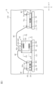
- FIG. 1 is a circuit diagram showing a schematic configuration of a signal transmission device according to an embodiment.
- FIG. 2 is a schematic plan view showing the internal structure of the signal transmission device of FIG.
- FIG. 3 is a schematic cross-sectional view showing an internal configuration of the signal transmission device of FIG.
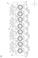
- FIG. 4 is a schematic plan view of the transformer chip of FIG.
- FIG. 5 is a schematic plan view of the transformer chip of FIG.
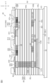
- FIG. 6 is a schematic cross-sectional view of the transformer chip taken along line F6-F6 in FIG.
- FIG. 7 is a schematic cross-sectional view of the transformer chip taken along line F7-F7 in FIG.
- FIG. 8 is a schematic cross-sectional view of the transformer chip taken along line F8-F8 in FIG.
- FIG. 1 is a circuit diagram showing a schematic configuration of a signal transmission device according to an embodiment.
- FIG. 2 is a schematic plan view showing the internal structure of the signal transmission device of FIG.
- FIG. 3 is a schematic
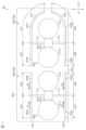
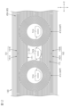
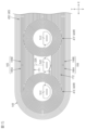
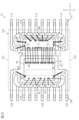
- FIG. 9 is a schematic plan view of the dummy wiring of the transformer chip.
- FIG. 10 is a schematic plan view showing an enlarged portion of the transformer chip of FIG.
- FIG. 11 is a schematic plan view showing an enlarged view of another part of the transformer chip of FIG.
- FIG. 12 is a schematic plan view showing an enlarged view of the first surface coil, the second surface coil, and the periphery of the transformer chip shown in FIG.
- FIG. 13 is a schematic plan view showing an enlargement of the first surface coil and its periphery in FIG.
- FIG. 14 is a schematic cross-sectional view showing an enlargement of the second surface coil and its periphery in FIG.
- FIG. 10 is a schematic plan view showing an enlarged portion of the transformer chip of FIG.
- FIG. 11 is a schematic plan view showing an enlarged view of another part of the transformer chip of FIG.
- FIG. 12 is a schematic plan view showing an enlarged view of the first surface coil, the second surface coil, and the peripher
- FIG. 15 is a schematic plan view showing an enlarged view of the fifth surface coil, the sixth surface coil, and the periphery of the transformer chip shown in FIG.
- FIG. 16 is a schematic plan view showing an enlargement of the fifth surface coil and its periphery in FIG.
- FIG. 17 is a schematic plan view showing an enlargement of the sixth surface coil and its periphery in FIG.
- FIG. 18 is a schematic plan view of a transformer chip of a comparative example.
- FIG. 19 is a schematic plan view of a transformer chip according to a modified example.
- FIG. 20 is a schematic plan view of a transformer chip according to a modified example.
- FIG. 21 is a schematic plan view showing an enlarged view of the first surface coil, the second surface coil, and the periphery of the transformer chip shown in FIG.
- FIG. 22 is a schematic plan view of a transformer chip according to a modified example.
- FIG. 23 is a circuit diagram showing a schematic configuration of a signal transmission device according to a modified example.
- FIG. 24 is a schematic plan view showing the internal configuration of the signal transmission device of FIG. 23.
- FIG. 25 is a schematic plan view showing an internal configuration of a signal transmission device according to a modified example.
- FIG. 26 is a schematic plan view showing an internal configuration of a signal transmission device according to a modified example.
- At least one means “one or more” of the desired options.
- at least one means “only one option” or “both of two options” if the number of options is two.
- at least one means “only one option” or “any combination of two or more options” if the number of options is three or more.
- the length of A is equal to the length of B
- the length of A and the length of B are equal to each other
- the difference between the length of A and the length of B is, for example, within 10% of the length of A.
- FIG. 1 shows a schematic circuit configuration of the signal transmission device 10 according to an embodiment.
- Figure 2 shows a schematic example of an internal configuration (planar structure) of the signal transmission device 10.
- Figure 3 shows a schematic example of a portion of the internal configuration (cross-sectional structure) of the signal transmission device 10. Note that hatched lines are omitted in Figure 3 to facilitate understanding of the drawing.
- the signal transmission device 10 includes a first circuit chip 60, a second circuit chip 70, and a transformer chip 80.
- the transformer chip 80 is connected between the first circuit chip 60 and the second circuit chip 70.
- the transformer chip 80 provides electrical insulation between the first circuit chip 60 and the second circuit chip 70.
- the first circuit chip 60 includes a first circuit 20 configured to operate with a first voltage V1.
- the first circuit 20 includes a transmitting circuit 21 and a receiving circuit 22.
- the second circuit chip 70 includes a second circuit 30 configured to operate with a second voltage V2.
- the second circuit 30 includes a receiving circuit 31 and a transmitting circuit 32.
- the first voltage V1 and the second voltage V2 may be the same as each other or may be different. In one example, the second voltage V2 is equal to the first voltage V1.
- the signal transmission device 10 may be referred to as a digital isolator.
- the transformer chip 80 includes a plurality of transformers 40.
- the plurality of transformers 40 include a first transformer 40A and a second transformer 40B connected to the transmitting circuit 21 of the first circuit 20, and a third transformer 40C and a fourth transformer 40D connected to the receiving circuit 22 of the first circuit 20.
- the first transformer 40A and the second transformer 40B are electrically connected between the transmitting circuit 21 of the first circuit chip 60 and the receiving circuit 31 of the second circuit chip 70.
- the third transformer 40C and the fourth transformer 40D are electrically connected between the receiving circuit 22 of the first circuit chip 60 and the transmitting circuit 32 of the second circuit chip 70.
- Each of the first to fourth transformers 40A to 40D includes a first coil 41 and a second coil 42.
- the first coil 41 of the first transformer 40A and the second transformer 40B is electrically connected to the receiving circuit 31 of the second circuit chip 70.
- the second coil 42 of the first transformer 40A and the second transformer 40B is electrically connected to the transmitting circuit 21 of the first circuit chip 60.
- the first coil 41 of the third transformer 40C and the fourth transformer 40D is electrically connected to the transmitting circuit 32 of the second circuit chip 70.
- the second coil 42 of the third transformer 40C and the fourth transformer 40D is electrically connected to the receiving circuit 22 of the first circuit chip 60.
- the transmitting circuit 21 of the first circuit chip 60 receives an input signal and pulse-drives the second coil 42 of at least one of the first transformer 40A and the second transformer 40B.
- the receiving circuit 31 of the second circuit chip 70 receives a signal that excites the first coil 41 of at least one of the first transformer 40A and the second transformer 40B and outputs an output signal.
- the transmitting circuit 32 of the second circuit chip 70 receives an input signal and pulse-drives the first coil 41 of at least one of the third transformer 40C and the fourth transformer 40D.
- the receiving circuit 22 of the first circuit chip 60 receives a signal that is excited in the second coil 42 of at least one of the third transformer 40C and the fourth transformer 40D and outputs an output signal.
- FIG. 2 shows an example of a schematic plan view showing the internal configuration of the signal transmission device 10.
- the number of external terminals of the signal transmission device 10 in Fig. 2 is greater than the number of external terminals of the signal transmission device 10 in Fig. 1.
- the number of external terminals of the signal transmission device 10 refers to the number of external electrodes capable of connecting the signal transmission device 10 to electronic components external to the signal transmission device 10.
- the number of signal lines (the number of wires W1 to W4 described later) that transmit signals from the first circuit 20 to the second circuit 30 in the signal transmission device 10 in Fig. 2 is greater than the number of signal lines in the signal transmission device 10 in Fig. 1.
- Figure 3 shows an example of a schematic cross-sectional view showing the internal configuration of the signal transmission device 10. Note that in Figure 3, the cross-sectional structures of each chip 60, 70, and 80 are shown in a simplified manner. Therefore, the cross-sectional structure of the transformer chip 80 shown in Figure 3 is different from the cross-sectional structure of the transformer chip 80 described later. The cross-sectional structure of the first transformer 40A is shown in the transformer chip 80 in Figure 3.
- the signal transmission device 10 is a semiconductor device in which a first circuit chip 60, a second circuit chip 70, and a transformer chip 80 are packaged together as multiple semiconductor chips.
- the package format of the signal transmission device 10 is an SO (Small Outline) type, which is an SOP (Small Outline Package) in this embodiment.
- the package format of the signal transmission device 10 can be changed as desired.
- the package format is not limited to SOP, and may be QFN (Quad For Non Lead Package), DFP (Dual Flat Package), DIP (Dual Inline Package), QFP (Quad Flat Package), SIP (Single Inline Package), or SOJ (Small Outline J-leaded Package), or various similar package structures.
- the first circuit chip 60 is mounted on the first lead frame 100.
- the second circuit chip 70 is mounted on the second lead frame 110.
- the transformer chip 80 is mounted on the first lead frame 100.
- both the first circuit chip 60 and the transformer chip 80 are mounted on the first lead frame 100.
- the sealing resin 120 seals a portion of each lead frame 100, 110 and each chip 60, 70, 80.
- the sealing resin 120 is shown by a two-dot chain line for the convenience of explaining the internal configuration of the signal transmission device 10.
- the sealing resin 120 is made of a resin material having electrical insulation properties.
- the resin material includes, for example, black epoxy resin.
- the sealing resin 120 is formed in a rectangular plate shape with the thickness direction being the Z direction.
- the sealing resin 120 has four resin side surfaces 121 to 124. More specifically, the sealing resin 120 has resin side surfaces 121 and 122 as both end faces in the X direction, and resin side surfaces 123 and 124 as both end faces in the Y direction.
- the X direction and the Y direction are directions perpendicular to the Z direction.
- the X direction and the Y direction are perpendicular to each other when viewed from the Z direction.
- the sealing resin 120 is rectangular in shape with the Y direction as the long side direction and the X direction as the short side direction when viewed from the Z direction.
- the X direction corresponds to the "first direction”
- the Y direction corresponds to the "second direction”.
- planear view means viewing from the Z direction.
- Each of the first lead frame 100 and the second lead frame 110 is a conductor and is made of a material containing, for example, Cu (copper), Fe (iron), Al (aluminum), etc.
- Each lead frame 100, 110 is provided across the inside and outside of the sealing resin 120.
- the first lead frame 100 has a first die pad 101 disposed within the sealing resin 120, and a plurality of first leads 102 disposed across the inside and outside of the sealing resin 120. Each of the first leads 102 constitutes an external terminal that electrically connects to an external electronic device of the signal transmission device 10.
- both the first circuit chip 60 and the transformer chip 80 are mounted on the first die pad 101.
- the first die pad 101 is positioned so that its center in the Y direction is closer to the resin side surface 123 than the center in the Y direction of the sealing resin 120. In this embodiment, the first die pad 101 is not exposed from the sealing resin 120.
- the shape of the first die pad 101 is rectangular with the long side direction in the X direction and the short side direction in the Y direction.
- the multiple first leads 102 are arranged at a distance from each other in the X direction. Of the multiple first leads 102, each of the first leads 102 arranged at both ends in the X direction is integrated with the first die pad 101. A portion of each first lead 102 protrudes outward from the resin side surface 123 of the sealing resin 120.
- the second lead frame 110 has a second die pad 111 disposed within the sealing resin 120, and a plurality of second leads 112 disposed across the inside and outside of the sealing resin 120.
- Each second lead 112 constitutes an external terminal that electrically connects to an external electronic device of the signal transmission device 10.
- the second circuit chip 70 is mounted on the second die pad 111.
- the second die pad 111 is disposed closer to the resin side surface 124 in the Y direction than the first die pad 101. In this embodiment, the second die pad 111 is not exposed from the sealing resin 120.
- the shape of the second die pad 111 is rectangular with the long side in the X direction and the short side in the Y direction.
- the first die pad 101 and the second die pad 111 are arranged at a distance from each other in the Y direction. Therefore, the Y direction can also be said to be the arrangement direction of both die pads 101, 111.
- the dimensions of the first die pad 101 and the second die pad 111 in the Y direction are set according to the size and number of semiconductor chips to be mounted.
- the first circuit chip 60 and the transformer chip 80 are mounted on the first die pad 101
- the second circuit chip 70 is mounted on the second die pad 111. Therefore, the dimension of the first die pad 101 in the Y direction is larger than the dimension of the second die pad 111 in the Y direction.
- the multiple second leads 112 are arranged at a distance from each other in the X direction. Of the multiple second leads 112, a pair of second leads 112 are integrated with the second die pad 111. A portion of each second lead 112 protrudes outward from the resin side surface 124 of the sealing resin 120.
- the number of second leads 112 is the same as the number of first leads 102.
- the multiple first leads 102 and the multiple second leads 112 are arranged in a direction (X direction) perpendicular to the arrangement direction (Y direction) of the first die pad 101 and the second die pad 111. Note that the number of second leads 112 and the number of first leads 102 can each be changed arbitrarily.
- the first die pad 101 is supported by a pair of first leads 102 that are integrated with the first die pad 101.
- the second die pad 111 is supported by a pair of second leads 112 that are integrated with the second die pad 111. Therefore, each die pad 101, 111 does not have a hanging lead exposed from the resin side surfaces 121, 122. This allows for a large insulation distance (creepage distance) between the first lead frame 100 and the second lead frame 110.
- the first circuit chip 60, the second circuit chip 70, and the transformer chip 80 are arranged at a distance from each other in the Y direction. In the Y direction, the first circuit chip 60, the transformer chip 80, and the second circuit chip 70 are arranged in this order from the first lead 102 to the second lead 112. Therefore, it can be said that the transformer chip 80 is disposed between the first circuit chip 60 and the second circuit chip 70 in the Y direction.
- the first circuit chip 60 is formed in a rectangular shape having short and long sides in a plan view. In a plan view, the first circuit chip 60 is mounted on the first die pad 101 so that the long sides run along the X direction and the short sides run along the Y direction. As shown in FIG. 3, the first circuit chip 60 has a chip main surface 60s and a chip back surface 60r that face opposite each other in the Z direction. The chip back surface 60r of the first circuit chip 60 is bonded to the first die pad 101 by a conductive bonding material SD.
- the conductive bonding material SD may be solder, Ag (silver) paste, or the like.
- the first circuit chip 60 includes the first circuit 20.
- a plurality of first electrode pads 61, a plurality of second electrode pads 62, and a plurality of third electrode pads 63 are formed on the chip main surface 60s of the first circuit chip 60.
- Each of the electrode pads 61 to 63 is electrically connected to the first circuit 20.
- the multiple first electrode pads 61 are arranged on the chip main surface 60s closer to the first lead 102 than the center of the chip main surface 60s in the Y direction.
- the multiple first electrode pads 61 are arranged in the X direction.
- the multiple second electrode pads 62 are arranged at the end of the chip main surface 60s in the Y direction that is closer to the transformer chip 80.
- the multiple second electrode pads 62 are arranged in the X direction.
- the multiple third electrode pads 63 are arranged at both ends of the chip main surface 60s in the X direction.
- the second circuit chip 70 is formed in a rectangular shape having short and long sides in a plan view. In a plan view, the second circuit chip 70 is mounted on the second die pad 111 so that the long sides run along the X direction and the short sides run along the Y direction. As shown in FIG. 3, the second circuit chip 70 has a chip main surface 70s and a chip back surface 70r that face opposite each other in the Z direction. The chip back surface 70r of the second circuit chip 70 is joined to the second die pad 111 by a conductive bonding material SD.
- the second circuit chip 70 includes a second circuit 30.
- a plurality of first electrode pads 71, a plurality of second electrode pads 72, and a plurality of third electrode pads 73 are formed on the chip main surface 70s of the second circuit chip 70.
- Each of the electrode pads 71 to 73 is electrically connected to the second circuit 30.
- the multiple first electrode pads 71 are arranged at the ends of the chip main surface 70s in the Y direction that are closer to the transformer chip 80.
- the multiple first electrode pads 71 are arranged in the X direction.
- the multiple second electrode pads 72 are arranged at the ends of the chip main surface 70s in the Y direction that are farther from the transformer chip 80. In other words, the multiple second electrode pads 72 are arranged at the ends of the chip main surface 70s in the Y direction that are closer to the second lead 112.
- the multiple second electrode pads 72 are arranged in the X direction.
- the multiple third electrode pads 73 are arranged at both ends of the chip main surface 70s in the X direction.
- the transformer chip 80 includes first to fourth transformers 40A to 40D (see FIG. 1) as multiple transformers 40.
- the transformer chip 80 is formed in a rectangular shape having short and long sides in a plan view.
- the transformer chip 80 is mounted on the first die pad 101 so that the long sides are aligned along the X direction and the short sides are aligned along the Y direction in a plan view.
- the transformer chip 80 has a chip main surface 80s and a chip back surface 80r that face opposite each other in the Z direction.
- the chip back surface 80r of the transformer chip 80 is bonded to the first die pad 101 by a conductive bonding material SD.
- a plurality of first electrode pads 81 and a plurality of second electrode pads 82 are formed on the chip main surface 80s of the transformer chip 80.
- the plurality of first electrode pads 81 are electrically connected to the first coils 41 (see FIG. 1) of the first to fourth transformers 40A to 40D
- the plurality of second electrode pads 82 are electrically connected to the second coils 42 (see FIG. 1) of the first to fourth transformers 40A to 40D.
- Both the first electrode pads 81 and the second electrode pads 82 include one or more appropriately selected from Ti (titanium), TiN (titanium nitride), Au (gold), Ag, Cu, Al, and W (tungsten).
- the multiple second electrode pads 82 are arranged, for example, at one of the two ends in the Y direction of the chip main surface 80s, which is closer to the first circuit chip 60.
- the multiple second electrode pads 82 are arranged in the X direction.
- the multiple first electrode pads 81 are arranged, for example, near the center in the Y direction of the chip main surface 80s.
- the multiple first electrode pads 81 are arranged in the X direction.
- the transformer chip 80 is disposed closer to the first circuit chip 60 than the second circuit chip 70. In other words, in a plan view, the distance between the second circuit chip 70 and the transformer chip 80 is greater than the distance between the first circuit chip 60 and the transformer chip 80.
- a number of wires W1 to W4 are connected to each of the first circuit chip 60, the transformer chip 80, and the second circuit chip 70.
- Each of the wires W1 to W4 is a bonding wire formed by a wire bonding device, and is made of a conductor containing, for example, Au, Al, Cu, etc.
- the first circuit chip 60 is electrically connected to the first lead frame 100 by the wire W1. More specifically, the first electrode pads 61 and the third electrode pads 63 of the first circuit chip 60 are connected to the first leads 102 by the wire W1. This electrically connects the first circuit 20 (see FIG. 1) to the first leads 102.
- the third electrode pads 63 of the first circuit chip 60 are connected to a pair of first leads 102 that are integrated with the first die pad 101 by the wire W1.
- the pair of first leads 102 that are integrated with the first die pad 101 constitute ground terminals, and the first circuit 20 and the first die pad 101 are electrically connected by the wire W1. Therefore, the first die pad 101 has the same potential as the ground GND1 of the first circuit 20.
- the second circuit chip 70 and each of the multiple second leads 112 of the second lead frame 110 are electrically connected by wires W4. More specifically, the multiple second electrode pads 72 and multiple third electrode pads 73 of the second circuit chip 70 are connected to the second leads 112 by wires W4. This electrically connects the second circuit 30 (see FIG. 1) and the multiple second leads 112.
- a pair of second leads 112 integrated with the second die pad 111 constitutes a ground terminal, and the second circuit 30 and the second die pad 111 are electrically connected by wires W4. Therefore, the second die pad 111 has the same potential as the ground GND2 of the second circuit 30.
- the transformer chip 80 is connected to the first circuit chip 60 by wire W2 and to the second circuit chip 70 by wire W3. More specifically, the multiple second electrode pads 82 of the transformer chip 80 are connected to the multiple second electrode pads 62 of the first circuit chip 60 by wire W2. This electrically connects the second coils 42 of the first to fourth transformers 40A to 40D to the first circuit 20. In addition, the multiple first electrode pads 81 of the transformer chip 80 are connected to the multiple first electrode pads 71 of the second circuit chip 70 by wire W3. This electrically connects the first coils 41 of the first to fourth transformers 40A to 40D to the second circuit 30.
- the second coils 42 of the first to fourth transformers 40A to 40D are electrically connected to the ground GND1 of the first circuit 20 via the wire W2 and the first circuit chip 60, etc.
- the first coils 41 of the first to fourth transformers 40A to 40D are electrically connected to the ground GND2 of the second circuit 30 via the wire W3 and the second circuit chip 70, etc.
- the configuration of the signal transmission device 10 shown in Figures 1 to 3 is an example, and the circuit configurations included in the first circuit chip 60 and the second circuit chip 70 may be changed as appropriate.
- the first circuit 20 may be configured to include a transmitting circuit 21 but not a receiving circuit 22.
- the second circuit 30 may be configured to include a receiving circuit 31 but not a transmitting circuit 32.
- the first circuit 20 may include circuits other than the transmitting circuit 21 and the receiving circuit 22.
- the second circuit 30 may include circuits other than the receiving circuit 31 and the transmitting circuit 32.
- the first circuit 20 may include an analog-to-digital conversion circuit.
- the signal transmission device 10 is configured as an isolated A/D conversion device.
- the second circuit 30 may include a driver circuit that drives the gate of the switching element.
- the driver circuit may be connected to an external terminal of the signal transmission device 10 (in one example, the second lead 112 shown in FIG. 2).
- the signal transmission device 10 is configured as an insulated gate driver that drives the switching element.
- the switching element is a power semiconductor element such as a SiMOSFET (Si Metal-Oxide-Semiconductor Field-Effect Transistor), a SiCMOSFET, or an IGBT (Insulated Gate Bipolar Transistor).
- the driver circuit generally uses a half-bridge circuit in which a low-side switching element and a high-side switching element are connected in a totem pole configuration.
- the signal transmission device 10 used as an insulated gate driver applies a drive voltage signal to the control terminal of the switching element.
- the transmission circuit 21 of the first circuit 20 converts a control signal input from, for example, a control device into a pulse signal.
- the driver circuit of the second circuit 30 outputs a drive voltage signal to the control terminal of the switching element based on a signal received by the reception circuit 31 through the first transformer 40A and the second transformer 40B.
- the transmission circuit 32 of the second circuit 30 and the reception circuit 22 of the first circuit 20 may be used to transmit a detection signal from, for example, a temperature sensor arranged near the motor to the control device.
- the power supply voltage of the first circuit 20 that receives a signal from the control device is 5V, 3.3V, etc., with respect to the ground potential.
- a voltage equivalent to the voltage applied to the drain of the high-side switching element (for example, 600V or more) is applied transiently.
- the signal transmission device 10 is required to have a dielectric strength voltage between the first circuit 20 and the second circuit 30, more specifically, between the first coil 41 and the second coil 42 of the first transformer 40A and the second transformer 40B.
- This dielectric strength voltage is 2500Vrms or more and 7500Vrms or less.
- the dielectric strength voltage of the signal transmission device 10 is about 5000Vrms.
- the specific value of the dielectric strength voltage of the signal transmission device 10 is not limited to this and is arbitrary.
- FIG. 4 is a schematic plan view showing the appearance of the transformer chip 80.
- FIG. 5 is a schematic plan view of the transformer chip 80 showing the positional relationship between the first electrode pad 81 and the second electrode pad 82 of the transformer chip 80 and the first to fourth transformers 40A to 40D.
- the passivation film 86 is omitted, and the first to fourth transformers 40A to 40D, the dummy wiring 45, and the floating dummy wiring 140 are each indicated by dashed lines.
- FIG. 6 is a schematic cross-sectional view of the transformer chip 80 taken along the XY plane at the Z-direction position of the second coils 42 of the first to fourth transformers 40A to 40D, showing the connection relationship of the second coils 42.
- FIG. 7 is a schematic cross-sectional view of the transformer chip 80 taken along the XY plane at the Z-direction position of the first coils 41 of the first to fourth transformers 40A to 40D, showing the connection relationship of the first coils 41. Note that hatching lines have been omitted in FIGS. 6 and 7 to make the drawings easier to understand.
- the transformer chip 80 includes two pairs of a first transformer 40A and a second transformer 40B, and two pairs of a third transformer 40C and a fourth transformer 40D.
- the transformer chip 80 is a semiconductor chip that integrates two pairs of a first transformer 40A and a second transformer 40B and two pairs of a third transformer 40C and a fourth transformer 40D into a single chip.
- the transformer chip 80 is provided separately from the first circuit chip 60 and the second circuit chip 70 (both see FIG. 2).
- the transformer chip 80 has chip side surfaces 80a to 80d.
- the chip side surfaces 80a and 80b form both end faces of the transformer chip 80 in the X direction
- the chip side surfaces 80c and 80d form both end faces of the transformer chip 80 in the Y direction.
- the chip side surfaces 80a and 80b form the short sides of the transformer chip 80
- the chip side surfaces 80c and 80d form the long sides of the transformer chip 80.
- the two pairs of the first to fourth transformers 40A to 40D are arranged closer to the chip side surface 80d than the center of the transformer chip 80 in the Y direction.
- the two pairs of the first to fourth transformers 40A to 40D are arranged at the same positions in the Y direction and spaced apart from each other in the X direction.
- the two pairs of the first to fourth transformers 40A to 40D are arranged in the following order from the chip side surface 80a to the chip side surface 80b: a pair of the first transformer 40A and the second transformer 40B, another pair of the first transformer 40A and the second transformer 40B, a pair of the third transformer 40C and the fourth transformer 40D, and another pair of the third transformer 40C and the fourth transformer 40D.
- the first transformer 40A is arranged closer to the chip side surface 80a than the second transformer 40B.
- the third transformer 40C is arranged closer to the chip side surface 80a than the fourth transformer 40D. Therefore, the two pairs of the first to fourth transformers 40A to 40D are arranged in the following order from the chip side surface 80a toward the chip side surface 80b: first transformer 40A, second transformer 40B, first transformer 40A, second transformer 40B, third transformer 40C, fourth transformer 40D, third transformer 40C, and fourth transformer 40D.
- the first to fourth transformers 40A to 40D have the same configuration.
- the transformer chip 80 of this embodiment includes the first isolation transformer 40P, the second isolation transformer 40Q, the third isolation transformer 40R, and the fourth isolation transformer 40S.
- the third isolation transformer 40R and the fourth isolation transformer 40S are distributed and arranged on both sides of the first isolation transformer 40P and the second isolation transformer 40Q in the X direction.
- the first isolation transformer 40P and the second isolation transformer 40Q are disposed between the third isolation transformer 40R and the fourth isolation transformer 40S in the X direction.
- the plurality of first electrode pads 81 include first to eighth pads 81A to 81H.
- the first pad 81A and the second pad 81B are pads electrically connected to the first transformer 40A and the second transformer 40B of the first isolation transformer 40P.
- the first pad 81A is arranged at a position overlapping the first transformer 40A and the second transformer 40B of the first isolation transformer 40P in a plan view.
- a plurality of first pads 81A are provided corresponding to the first transformer 40A and the second transformer 40B. That is, the plurality of first pads 81A include the first pad 81A electrically connected to the first transformer 40A and the first pad 81A electrically connected to the second transformer 40B.
- the second pad 81B is arranged outside the first transformer 40A and the second transformer 40B.
- the second pad 81B is arranged between the first transformer 40A and the second transformer 40B in the X direction.
- the second pad 81B is electrically connected to both the first transformer 40A and the second transformer 40B.
- the second pad 81B is provided as a common pad for the first transformer 40A and the second transformer 40B.
- the second pad 81B is an example of a "first outer pad.”
- the third pad 81C and the fourth pad 81D are pads electrically connected to the third transformer 40C and the fourth transformer 40D of the second isolation transformer 40Q.
- the third pad 81C is arranged at a position overlapping the third transformer 40C and the fourth transformer 40D of the second isolation transformer 40Q in a plan view.
- a plurality of third pads 81C are provided corresponding to the third transformer 40C and the fourth transformer 40D.
- the plurality of third pads 81C include a third pad 81C electrically connected to the third transformer 40C and a third pad 81C electrically connected to the fourth transformer 40D.
- the fourth pad 81D is arranged outside the third transformer 40C and the fourth transformer 40D.
- the fourth pad 81D is arranged between the third transformer 40C and the fourth transformer 40D in the X direction.
- the fourth pad 81D is electrically connected to both the third transformer 40C and the fourth transformer 40D.
- the fourth pad 81D is provided as a common pad for the third transformer 40C and the fourth transformer 40D.
- the fourth pad 81D is an example of a "second outer pad.”
- the fifth pad 81E and the sixth pad 81F are pads electrically connected to the first transformer 40A and the second transformer 40B of the third isolation transformer 40R.
- the fifth pad 81E is arranged at a position overlapping the first transformer 40A and the second transformer 40B of the third isolation transformer 40R in a plan view.
- a plurality of fifth pads 81E are provided corresponding to the first transformer 40A and the second transformer 40B.
- the plurality of fifth pads 81E include the fifth pad 81E electrically connected to the first transformer 40A and the fifth pad 81E electrically connected to the second transformer 40B.
- the sixth pad 81F is arranged outside the first transformer 40A and the second transformer 40B.
- the sixth pad 81F is arranged between the first transformer 40A and the second transformer 40B in the X direction.
- the sixth pad 81F is electrically connected to both the first transformer 40A and the second transformer 40B.
- the sixth pad 81F is provided as a common pad for the first transformer 40A and the second transformer 40B.
- the seventh pad 81G and the eighth pad 81H are pads electrically connected to the third transformer 40C and the fourth transformer 40D of the fourth isolation transformer 40S.
- the seventh pad 81G is arranged at a position overlapping the third transformer 40C and the fourth transformer 40D of the fourth isolation transformer 40S in a plan view.
- a plurality of seventh pads 81G are provided corresponding to the third transformer 40C and the fourth transformer 40D.
- the plurality of seventh pads 81G include a seventh pad 81G electrically connected to the third transformer 40C and a seventh pad 81G electrically connected to the fourth transformer 40D.
- the eighth pad 81H is arranged outside the third transformer 40C and the fourth transformer 40D.
- the eighth pad 81H is arranged between the third transformer 40C and the fourth transformer 40D in the X direction.
- the eighth pad 81H is electrically connected to both the third transformer 40C and the fourth transformer 40D.
- the eighth pad 81H is provided as a common pad for the third transformer 40C and the fourth transformer 40D.
- the multiple second electrode pads 82 are arranged closer to the chip side surface 80c than the first to fourth transformers 40A to 40D in a plan view.
- the multiple second electrode pads 82 are arranged at one of the two ends of the transformer chip 80 in the Y direction that is closer to the chip side surface 80c. It can also be said that the multiple second electrode pads 82 are arranged closer to the first lead 102 (see Figure 2) than the two pairs of the first to fourth transformers 40A to 40D in a plan view.
- the multiple second electrode pads 82 are arranged in the same position as the two pairs of the first to fourth transformers 40A to 40D in the X direction.
- the second electrode pad 82 includes first to eighth pads 82A to 82H.
- the first pad 82A corresponds to the first pad 81A of the first electrode pad 81
- the second pad 82B corresponds to the second pad 81B of the first electrode pad 81
- the third pad 82C corresponds to the third pad 81C of the first electrode pad 81
- the fourth pad 82D corresponds to the fourth pad 81D of the first electrode pad 81.
- the fifth pad 82E corresponds to the fifth pad 81E of the first electrode pad 81
- the sixth pad 82F corresponds to the sixth pad 81F of the first electrode pad 81
- the seventh pad 82G corresponds to the seventh pad 81G of the first electrode pad 81
- the eighth pad 82H corresponds to the eighth pad 81H of the first electrode pad 81.
- the first pad 82A and the second pad 82B are electrically connected to the first transformer 40A and the second transformer 40B of the first isolation transformer 40P.
- the third pad 82C and the fourth pad 82D are electrically connected to the third transformer 40C and the fourth transformer 40D of the second isolation transformer 40Q.
- the fifth pad 82E and the sixth pad 82F are electrically connected to the first transformer 40A and the second transformer 40B of the third isolation transformer 40R.
- the seventh pad 82G and the eighth pad 82H are electrically connected to the third transformer 40C and the fourth transformer 40D of the fourth isolation transformer 40S.
- a plurality of first pads 82A are provided corresponding to the first transformer 40A and the second transformer 40B of the first isolation transformer 40P.
- the plurality of first pads 82A include a first pad 82A electrically connected to the first transformer 40A and a first pad 82A electrically connected to the second transformer 40B.
- the second pad 82B is electrically connected to both the first transformer 40A and the second transformer 40B.
- the second pad 82B can be said to be provided as a common pad for the first transformer 40A and the second transformer 40B.
- the third pads 82C are provided in multiple locations corresponding to the third transformer 40C and the fourth transformer 40D of the second isolation transformer 40Q. That is, the multiple third pads 82C include a third pad 82C electrically connected to the third transformer 40C and a third pad 82C electrically connected to the fourth transformer 40D.
- the fourth pad 82D is electrically connected to both the third transformer 40C and the fourth transformer 40D. That is, the fourth pad 82D can be said to be provided as a common pad for the third transformer 40C and the fourth transformer 40D.
- the fifth pad 82E is provided in multiple locations corresponding to the first transformer 40A and the second transformer 40B of the third isolation transformer 40R. That is, the multiple fifth pads 82E include a fifth pad 82E electrically connected to the first transformer 40A and a fifth pad 82E electrically connected to the second transformer 40B.
- the sixth pad 82F is electrically connected to both the first transformer 40A and the second transformer 40B. That is, the sixth pad 82F can be said to be provided as a common pad for the first transformer 40A and the second transformer 40B.
- the seventh pad 82G is provided in multiple locations corresponding to the third transformer 40C and the fourth transformer 40D of the fourth isolation transformer 40S.
- the multiple seventh pads 82G include a seventh pad 82G electrically connected to the third transformer 40C and a seventh pad 82G electrically connected to the fourth transformer 40D.
- the eighth pad 82H is electrically connected to both the third transformer 40C and the fourth transformer 40D. In other words, the eighth pad 82H can be said to be provided as a common pad for the third transformer 40C and the fourth transformer 40D.
- (Cross-sectional structure of transformer chip) 8 is a schematic cross-sectional view of a transformer chip 80 mainly showing the cross-sectional structure of a transformer 40 A.
- the cross-sectional structure of the transformer chip 80 will be described below with reference to FIGS.
- a transformer chip 80 has a substrate 83 and an insulating layer 84 formed on the substrate 83 .
- the substrate 83 is, for example, a semiconductor substrate.
- the substrate 83 is a substrate formed of a material containing Si (silicon).
- Examples of the Si substrate used for the substrate 83 include a semiconductor substrate made of a single crystal intrinsic semiconductor material, a p-type semiconductor substrate containing an acceptor-type impurity, and an n-type semiconductor substrate containing a donor-type impurity.
- the substrate 83 may be a semiconductor substrate using a wide band gap semiconductor or a compound semiconductor.
- the wide band gap semiconductor is a semiconductor substrate having a band gap of 2.0 eV or more.
- the wide band gap semiconductor may be SiC (silicon carbide), GaN (gallium nitride), Ga 2 O 3 (gallium oxide), or the like.
- the compound semiconductor may be a III-V group compound semiconductor.
- the compound semiconductor may include at least one of AlN (aluminum nitride), InN (indium nitride), GaN, and GaAs (gallium arsenide).
- the substrate 83 may be an insulating substrate formed of a material including glass, instead of a semiconductor substrate.
- the substrate 83 has a substrate main surface 83s and a substrate back surface 83r that face opposite each other in the Z direction.
- the substrate main surface 83s faces the same side as the chip main surface 80s of the transformer chip 80
- the substrate back surface 83r faces the same side as the chip back surface 80r of the transformer chip 80.
- the substrate back surface 83r constitutes the chip back surface 80r of the transformer chip 80.
- the insulating layer 84 has a plurality of insulating films 85 stacked in the Z direction from the substrate main surface 83s of the substrate 83.
- the Z direction can be said to be the thickness direction of the insulating layer 84.
- the Z direction can also be said to be the stacking direction of the plurality of insulating films 85.
- the insulating layer 84 is formed on the substrate main surface 83s of the substrate 83.
- the insulating layer 84 includes an upper surface 84s and a lower surface 84r facing the opposite side to the upper surface 84s.
- the lower surface 84r is in contact with the substrate main surface 83s.
- the upper surface 84s is an example of the "surface of the insulating layer”
- the lower surface 84r is an example of the "rear surface of the insulating layer”.
- the insulating film 85 includes a first insulating film 85A and a second insulating film 85B formed on the first insulating film 85A.
- the first insulating film 85A is a thin film, for example, an etching stopper layer.
- the first insulating film 85A is formed of a material including SiN (silicon nitride), SiC, SiCN (nitrogen-added silicon carbide), or the like.
- the first insulating film 85A is formed of a material including SiN.
- the second insulating film 85B is, for example, an interlayer insulating film.
- the second insulating film 85B is formed of a material including SiO (silicon oxide), for example.
- the second insulating film 85B is formed of SiO 2.
- the thickness of the second insulating film 85B is thicker than the thickness of the first insulating film 85A.
- the thickness of the first insulating film 85A may be, for example, 100 nm or more and less than 1000 nm.
- the thickness of the second insulating film 85B may be, for example, 1000 nm or more and 3000 nm or less.
- the first insulating film 85A has a thickness of, for example, about 300 nm
- the second insulating film 85B has a thickness of, for example, about 2000 nm.
- the bottom insulating film 85L in contact with the substrate main surface 83s of the substrate 83 and the top insulating film 85U are both composed of the second insulating film 85B.
- the thicknesses of both the bottom insulating film 85L and the top insulating film 85U are thinner than the other insulating films 85.
- the thicknesses of both the bottom insulating film 85L and the top insulating film 85U are greater than or equal to the thickness of the first insulating film 85A and less than or equal to the thickness of the second insulating film 85B.
- the thickness of both the bottom insulating film 85L and the top insulating film 85U can be changed as desired.
- the thickness of both the bottom insulating film 85L and the top insulating film 85U may be thicker than the thickness of the second insulating film 85B, or may be greater than or equal to the thickness of the insulating film 85 formed by the first insulating film 85A and the second insulating film 85B.
- the transformer chip 80 includes a passivation film 86.
- the passivation film 86 is formed on the upper surface 84s of the insulating layer 84.
- the passivation film 86 is a film that protects the insulating layer 84, and can also be said to be a surface protective film for the transformer chip 80.
- the passivation film 86 is formed of a material that includes, for example, any one of SiO, SiN, and SiCN.
- the upper surface of the passivation film 86 constitutes the chip main surface 80s of the transformer chip 80.
- Each electrode pad 81, 82 is covered with a passivation film 86.
- the passivation film 86 has an opening that exposes a portion of each electrode pad 81, 82.
- the second electrode pad 82 has an exposed surface for connecting the wire W2 (see FIG. 2).
- the first electrode pad 81 has an exposed surface for connecting the wire W3 (see FIG. 2).
- the transformer chip 80 includes a resin layer 87 formed on a passivation film 86.
- the resin layer 87 is formed of a material containing, for example, polyimide (PI).
- the resin layer 87 is separated into an inner resin layer and an outer resin layer by a separation groove 87A.
- the separation groove 87A is formed in a rectangular ring shape in a plan view.
- the separation groove 87A is formed so as to surround two pairs of the first to fourth transformers 40A to 40D in a plan view.
- the separation groove 87A is formed so as to surround the first to fourth isolation transformers 40P, 40Q, 40R, and 40S in a plan view.
- the resin layer 87 includes a first resin opening 87B that exposes the second electrode pad 82 and a second resin opening 87C that exposes the first electrode pad 81.
- the exposed surface of the second electrode pad 82 is exposed to the outside of the transformer chip 80 through the first resin opening 87B and the opening of the passivation film 86 (see FIG. 8).
- the exposed surface of the first electrode pad 81 is exposed to the outside of the transformer chip 80 through the second resin opening 87C and the opening of the passivation film 86.
- the second coils 42 of the two pairs of the first to fourth transformers 40A to 40D include the first to eighth back coils 42A to 42H. More specifically, the second coil 42 of the first transformer 40A of the first isolation transformer 40P is the "first back coil 42A”, and the second coil 42 of the second transformer 40B of the first isolation transformer 40P is the “second back coil 42B”. The second coil 42 of the third transformer 40C of the second isolation transformer 40Q is the “third back coil 42C", and the second coil 42 of the fourth transformer 40D of the second isolation transformer 40Q is the "fourth back coil 42D".
- the second coil 42 of the first transformer 40A of the third isolation transformer 40R is the "fifth back coil 42E", and the second coil 42 of the second transformer 40B of the third isolation transformer 40R is the "sixth back coil 42F”.
- the second coil 42 of the third transformer 40C of the fourth isolation transformer 40S is the "seventh back coil 42G", and the second coil 42 of the fourth transformer 40D of the fourth isolation transformer 40S is the "eighth back coil 42H".
- the first to eighth rear coils 42A to 42H are configured with second coil wiring 44.
- the second coil wiring 44 is formed in a spiral shape in a plan view.
- the second coil wiring 44 includes one or more appropriately selected from Ti, TiN, Au, Ag, Cu, Al, and W.
- the first to eighth back coils 42A to 42H are formed in an annular shape.
- the first to eighth back coils 42A to 42H have the winding directions of adjacent back coils in the X direction opposite to each other.
- the second back coil 42B is formed by winding the second coil wiring 44 in a winding direction opposite to that of the first back coil 42A in a plan view.
- the fourth back coil 42D is formed by winding the second coil wiring 44 in a winding direction opposite to that of the third back coil 42C in a plan view.
- the sixth back coil 42F is formed by winding the second coil wiring 44 in a winding direction opposite to that of the fifth back coil 42E in a plan view.
- the eighth back coil 42H is formed by winding the second coil wiring 44 in a winding direction opposite to that of the seventh back coil 42G in a plan view. Additionally, the number of turns of the second coil wiring 44 in the first to eighth back coils 42A to 42H are the same.
- An inner end wiring 57A is arranged inside the second coil wiring 44 of each of the first back surface coil 42A and the second back surface coil 42B, and an outer end wiring 58A is arranged outside the second coil wiring 44 of each of the first back surface coil 42A and the second back surface coil 42B.
- One end of the second coil wiring 44 of each of the first back surface coil 42A and the second back surface coil 42B is electrically connected to the inner end wiring 57A, and the other end of the second coil wiring 44 is electrically connected to the outer end wiring 58A.
- the outer end wiring 58A is configured as a common end wiring for the first back surface coil 42A and the second back surface coil 42B.
- An inner end wiring 57B is arranged inside the second coil wiring 44 of each of the third back surface coil 42C and the fourth back surface coil 42D, and an outer end wiring 58B is arranged outside the second coil wiring 44 of each of the third back surface coil 42C and the fourth back surface coil 42D.
- One end of the second coil wiring 44 of each of the third back surface coil 42C and the fourth back surface coil 42D is electrically connected to the inner end wiring 57B, and the other end of the second coil wiring 44 is electrically connected to the outer end wiring 58B.
- the outer end wiring 58B is configured as a common end wiring for the third back surface coil 42C and the fourth back surface coil 42D.
- An inner end wiring 57C is arranged inside the second coil wiring 44 of each of the fifth back surface coil 42E and the sixth back surface coil 42F, and an outer end wiring 58C is arranged outside the second coil wiring 44 of each of the fifth back surface coil 42E and the sixth back surface coil 42F.
- One end of the second coil wiring 44 of each of the fifth back surface coil 42E and the sixth back surface coil 42F is electrically connected to the inner end wiring 57C, and the other end of the second coil wiring 44 is electrically connected to the outer end wiring 58C.
- the outer end wiring 58C is configured as a common end wiring for the fifth back surface coil 42E and the sixth back surface coil 42F.
- the inner end wiring 57D is arranged inside the second coil wiring 44 of each of the seventh back coil 42G and the eighth back coil 42H, and the outer end wiring 58D is arranged outside the second coil wiring 44 of each of the seventh back coil 42G and the eighth back coil 42H.
- One end of the second coil wiring 44 of each of the seventh back coil 42G and the eighth back coil 42H is electrically connected to the inner end wiring 57D, and the other end of the second coil wiring 44 is electrically connected to the outer end wiring 58D.
- the outer end wiring 58D is configured as a common end wiring for the seventh back coil 42G and the eighth back coil 42H.
- Each of the inner end wirings 57A to 57D and the outer end wirings 58A to 58D includes a material selected from one or more of Ti, TiN, Au, Ag, Cu, Al, and W.
- one end of the second coil wiring 44 is an inner end of the spiral-shaped second coil wiring 44 in a plan view.
- the other end of the second coil wiring 44 is an outer end of the spiral-shaped second coil wiring 44 in a plan view.
- the configuration of the outer end wirings 58A to 58D can be changed as desired.
- the outer end wiring 58A may be provided for each of the first back surface coil 42A and the second back surface coil 42B.
- the outer end wiring 58B may be provided for each of the third back surface coil 42C and the fourth back surface coil 42D.
- the outer end wiring 58C may be provided for each of the fifth back surface coil 42E and the sixth back surface coil 42F.
- the outer end wiring 58D may be provided for each of the seventh back surface coil 42G and the eighth back surface coil 42H.
- the inner end wiring 57A is electrically connected to the first pad 82A by the connection wiring 131A.
- the inner end wiring 57B is electrically connected to the third pad 82C by the connection wiring 131C.
- the inner end wiring 57C is electrically connected to the fifth pad 82E by the connection wiring 131E.
- the inner end wiring 57D is electrically connected to the seventh pad 82G by the connection wiring 131G.
- the connection wirings 131A, 131C, 131E, and 131G include one or more appropriately selected materials selected from Ti, TiN, Au, Ag, Cu, Al, and W.
- the connection wirings 131C, 131E, and 131G have the same configuration as the connection wiring 131A. Therefore, in the following, the configuration of the connection wiring 131A will be described, and detailed configurations of the connection wirings 131C, 131E, and 131G will be omitted.
- the connection wiring 131A includes a first wiring portion 132A extending in the Z direction so as to penetrate a plurality of insulating films 85, and a second wiring portion 133A extending in the Y direction.
- the first wiring portion 132A is disposed at a position overlapping the first pad 82A in a plan view, and is connected to the first pad 82A.
- the first wiring portion 132A penetrates from the insulating film 85 below the uppermost insulating film 85U to the insulating film 85 above the lowermost insulating film 85L.
- the first wiring portion 132A includes a flat wiring portion and a plurality of vias.
- the wiring portion is provided at the same position as the insulating films 85P and 85Q on which the coils 41 and 42 are provided.
- the plurality of vias are provided between the two wiring portions in the Z direction, between the upper wiring portion and the first pad 82A, and between the lower wiring portion and the second wiring portion 133A.
- the second wiring portion 133A is provided closer to the substrate 83 than the first wiring portion 132A.
- the second wiring portion 133A is provided closer to the substrate 83 than the first back coil 42A.
- the second wiring portion 133A is provided in an insulating film 85 that is one layer above the lowest insulating film 85L among the multiple insulating films 85.
- the first end closer to the chip side surface 80c of the transformer chip 80 is provided at a position overlapping with the first wiring portion 132A in a planar view.
- the second wiring portion 133A is connected to the first wiring portion 132A.
- the second end of the second wiring portion 133A which is opposite to the first end, is provided at a position overlapping with the first back coil 42A in a planar view. More specifically, the second end is provided at a position overlapping with the inner end wiring 57A to which the first back coil 42A is connected in a planar view.
- the connection wiring 131A includes a plurality of vias 134A that connect the second wiring portion 133A and the inner end wiring 57A. As shown in FIG. 6, the connection wirings 131C, 131E, and 131G include first wiring portions 132C, 132E, and 132G, second wiring portions 133C, 133E, and 133G, and a plurality of vias (not shown), similar to the connection wiring 131A.
- the outer end wiring 58A is electrically connected to the second pad 82B by the connection wiring 131B.
- the outer end wiring 58B is electrically connected to the fourth pad 82D by the connection wiring 131D.
- the outer end wiring 58C is electrically connected to the sixth pad 82F by the connection wiring 131F.
- the outer end wiring 58D is electrically connected to the eighth pad 82H by the connection wiring 131H.
- the connection wirings 131B, 131D, 131F, and 131H include one or more appropriately selected materials selected from Ti, TiN, Au, Ag, Cu, Al, and W.
- the connection wirings 131B, 131D, 131F, and 131H include the same configuration as the connection wiring 131A.
- connection wirings 131B, 131D, 131F, and 131H include first wiring portions 132B, 132D, 132F, and 132H, second wiring portions 133B, 133D, 133F, and 133H, and a plurality of vias (not shown) similar to the connection wiring 131A.
- the connection wirings 131B, 131D, 131F, and 131H include substrate-side vias (not shown) that connect the second wiring portions 133B, 133D, 133F, and 133H to the substrate 83.
- the connection wirings 131B, 131D, 131F, and 131H are electrically connected to the substrate 83.
- the first coils 41 of the two pairs of the first to fourth transformers 40A to 40D include first to eighth surface coils 41A to 41H. More specifically, the first coil 41 of the first transformer 40A of the first isolation transformer 40P is the "first surface coil 41A”, and the first coil 41 of the second transformer 40B of the first isolation transformer 40P is the “second surface coil 41B”. The first coil 41 of the third transformer 40C of the second isolation transformer 40Q is the “third surface coil 41C", and the first coil 41 of the fourth transformer 40D of the second isolation transformer 40Q is the "fourth surface coil 41D".
- the first coil 41 of the first transformer 40A of the third isolation transformer 40R is the "fifth surface coil 41E"
- the first coil 41 of the second transformer 40B of the third isolation transformer 40R is the "sixth surface coil 41F”.
- the first coil 41 of the third transformer 40C of the fourth isolation transformer 40S is the "seventh surface coil 41G”
- the first coil 41 of the fourth transformer 40D of the fourth isolation transformer 40S is the "eighth surface coil 41H.”
- the first to eighth surface coils 41A to 48A are formed of the first coil wiring 43.
- the first coil wiring 43 is formed in a spiral shape when viewed in a plane.
- the second coil 42 includes one or more appropriately selected from Ti, TiN, Au, Ag, Cu, Al, and W.
- each of the first to eighth surface coils 41A to 41H is formed in a circular ring shape.
- the first to eighth surface coils 41A to 41H have the winding directions of adjacent surface coils in the X direction opposite to each other.
- the second surface coil 41B is formed by winding the first coil wiring 43 in a winding direction opposite to that of the first surface coil 41A in a plan view.
- the fourth surface coil 41D is formed by winding the first coil wiring 43 in a winding direction opposite to that of the third surface coil 41C in a plan view.
- the sixth surface coil 41F is formed by winding the first coil wiring 43 in a winding direction opposite to that of the fifth surface coil 41E in a plan view.
- the eighth surface coil 41H is formed by winding the first coil wiring 43 in a winding direction opposite to that of the seventh surface coil 41G in a plan view.
- the number of turns of the first coil wiring 43 in the first to eighth surface coils 41A to 41H is the same as each other.
- the first coil wiring 43 is formed in the same winding direction as the second coil wiring 44 shown in FIG. 6 in a plan view.
- the number of turns of the first coil wiring 43 in the first to eighth surface coils 41A to 41H is the same as the number of turns of the second coil wiring 44 in the first to eighth back surface coils 42A to 42H.
- the first pad 81A is disposed at a position overlapping the first surface coil 41A and the second surface coil 41B in a plan view.
- the second pad 81B is disposed at a position overlapping between the first surface coil 41A and the second surface coil 41B in a plan view. It can be said that the second pad 81B is disposed outside the first coil wiring 43 of the first surface coil 41A and the second surface coil 41B.
- One end of the first coil wiring 43 of the first surface coil 41A and the second surface coil 41B is electrically connected to the first pad 81A.
- the other end of the first coil wiring 43 of the first surface coil 41A and the second surface coil 41B is electrically connected to the second pad 81B. Therefore, the second pad 81B is configured as a common pad for the first surface coil 41A and the second surface coil 41B.
- the third pad 81C is arranged at a position overlapping the third surface coil 41C and the fourth surface coil 41D in a planar view.
- the fourth pad 81D is arranged at a position overlapping between the third surface coil 41C and the fourth surface coil 41D in a planar view. It can be said that the fourth pad 81D is arranged outside the first coil wiring 43 of the third surface coil 41C and the fourth surface coil 41D.
- One end of the first coil wiring 43 of the third surface coil 41C and the fourth surface coil 41D is electrically connected to the third pad 81C.
- the other end of the first coil wiring 43 of the third surface coil 41C and the fourth surface coil 41D is electrically connected to the fourth pad 81D. Therefore, the fourth pad 81D is configured as a common pad for the third surface coil 41C and the fourth surface coil 41D.
- the fifth pad 81E is arranged at a position overlapping the fifth surface coil 41E and the sixth surface coil 41F in a plan view.
- the sixth pad 81F is arranged at a position overlapping between the fifth surface coil 41E and the sixth surface coil 41F in a plan view. It can be said that the sixth pad 81F is arranged outside the first coil wiring 43 of the fifth surface coil 41E and the sixth surface coil 41F.
- One end of the first coil wiring 43 of the fifth surface coil 41E and the sixth surface coil 41F is electrically connected to the fifth pad 81E.
- the other end of the first coil wiring 43 of the fifth surface coil 41E and the sixth surface coil 41F is electrically connected to the sixth pad 81F. Therefore, the sixth pad 81F is configured as a common pad for the fifth surface coil 41E and the sixth surface coil 41F.
- the seventh pad 81G is disposed at a position overlapping the seventh surface coil 41G and the eighth surface coil 41H in a plan view.
- the eighth pad 81H is disposed at a position overlapping between the seventh surface coil 41G and the eighth surface coil 41H in a plan view. It can be said that the eighth pad 81H is disposed outside the first coil wiring 43 of the seventh surface coil 41G and the eighth surface coil 41H.
- One end of the first coil wiring 43 of the seventh surface coil 41G and the eighth surface coil 41H is electrically connected to the seventh pad 81G.
- the other end of the first coil wiring 43 of the seventh surface coil 41G and the eighth surface coil 41H is electrically connected to the eighth pad 81H. Therefore, the eighth pad 81H is configured as a common pad for the seventh surface coil 41G and the eighth surface coil 41H.
- the configuration of the second pad 81B, the fourth pad 81D, the sixth pad 81F, and the eighth pad 81H can be changed as desired.
- the second pad 81B may be provided for the first surface coil 41A and the second surface coil 41B, respectively.
- the fourth pad 81D may be provided for the third surface coil 41C and the fourth surface coil 41D, respectively.
- the sixth pad 81F may be provided for the fifth surface coil 41E and the sixth surface coil 41F, respectively.
- the eighth pad 81H may be provided for the seventh surface coil 41G and the eighth surface coil 41H, respectively.
- an inner end wiring 51A is arranged inside the first coil wiring 43 of each of the first surface coil 41A and the second surface coil 41B, and an outer end wiring 52A is arranged outside the first coil wiring 43 of the first surface coil 41A and the second surface coil 41B.
- One end of the first coil wiring 43 of the first surface coil 41A and the second surface coil 41B is electrically connected to the inner end wiring 51A, and the other end of the first coil wiring 43 is electrically connected to the outer end wiring 52A.
- the outer end wiring 52A is configured as a common end wiring for the first surface coil 41A and the second surface coil 41B.
- Inner end wiring 51B is arranged inside the first coil wiring 43 of each of the third surface coil 41C and the fourth surface coil 41D, and outer end wiring 52B is arranged outside the first coil wiring 43 of the third surface coil 41C and the fourth surface coil 41D.
- One end of the first coil wiring 43 of the third surface coil 41C and the fourth surface coil 41D is electrically connected to the inner end wiring 51B, and the other end of the first coil wiring 43 is electrically connected to the outer end wiring 52B.
- the outer end wiring 52B is configured as a common end wiring for the third surface coil 41C and the fourth surface coil 41D.
- An inner end wiring 51C is arranged inside the first coil wiring 43 of each of the fifth surface coil 41E and the sixth surface coil 41F, and an outer end wiring 52C is arranged outside the first coil wiring 43 of the fifth surface coil 41E and the sixth surface coil 41F.
- One end of the first coil wiring 43 of the fifth surface coil 41E and the sixth surface coil 41F is electrically connected to the inner end wiring 51C, and the other end of the first coil wiring 43 is electrically connected to the outer end wiring 52C.
- the outer end wiring 52C is configured as a common end wiring for the fifth surface coil 41E and the sixth surface coil 41F.
- the inner end wiring 51D is arranged inside the first coil wiring 43 of each of the seventh surface coil 41G and the eighth surface coil 41H, and the outer end wiring 52D is arranged outside the first coil wiring 43 of the seventh surface coil 41G and the eighth surface coil 41H.
- One end of the first coil wiring 43 of the seventh surface coil 41G and the eighth surface coil 41H is electrically connected to the inner end wiring 51D, and the other end of the first coil wiring 43 is electrically connected to the outer end wiring 52D.
- the outer end wiring 52D is configured as a common end wiring for the seventh surface coil 41G and the eighth surface coil 41H.
- the inner end wirings 51A to 51D and the outer end wirings 52A to 52D include a material selected from one or more of Ti, TiN, Au, Ag, Cu, Al, and W.
- one end of the first coil wiring 43 is an inner end of the first coil wiring 43 that is spiral-shaped in a plan view.
- the other end of the first coil wiring 43 is an outer end of the first coil wiring 43 that is spiral-shaped in a plan view.
- the configuration of the outer end wirings 52A to 52D can be changed as desired.
- the outer end wiring 52A may be provided for each of the first surface coil 41A and the second surface coil 41B.
- the outer end wiring 52B may be provided for each of the third surface coil 41C and the fourth surface coil 41D.
- the outer end wiring 52C may be provided for each of the fifth surface coil 41E and the sixth surface coil 41F.
- the outer end wiring 52D may be provided for each of the seventh surface coil 41G and the eighth surface coil 41H.
- the inner end wiring 51A is disposed at a position overlapping the first pad 81A in a plan view.
- the inner end wiring 51A is electrically connected to the first pad 81A by a via 53.
- the via 53 penetrates the uppermost insulating film 85U.
- the connection structure between the inner end wiring 51B and the third pad 81C, the connection structure between the inner end wiring 51C and the fifth pad 81E, and the connection structure between the inner end wiring 51D and the seventh pad 81G are the same as the connection structure between the inner end wiring 51A and the first pad 81A.
- connection structure between the outer end wiring 52A and the second pad 81B, the connection structure between the outer end wiring 52B and the fourth pad 81D, the connection structure between the outer end wiring 52C and the sixth pad 81F, and the connection structure between the outer end wiring 52D and the eighth pad 81H are also the same as the connection structure between the inner end wiring 51A and the first pad 81A.
- the transformer chip 80 includes dummy wiring 45 formed around the first to eighth surface coils 41A to 41H.
- the dummy wiring 45 is a wiring pattern formed so that no current flows through the first coil wiring 43 of the first to eighth surface coils 41A to 41H.
- the dummy wiring 45 is disposed in the same position in the Z direction as the first to eighth surface coils 41A to 41H.
- the dummy wiring 45 includes one or more appropriately selected from Ti, TiN, Au, Ag, Cu, Al, and W. The detailed configuration of the dummy wiring 45 will be described later.
- the transformer chip 80 further includes floating dummy wiring 140 that surrounds the first to eighth surface coils 41A to 41H and the dummy wiring 45 in a plan view and is insulated from the dummy wiring 45.
- the floating dummy wiring 140 is disposed in the same position as the first to eighth surface coils 41A to 41H and the dummy wiring 45 in the Z direction.
- the floating dummy wiring 140 is also insulated from the first to eighth surface coils 41A to 41H.
- the floating dummy wiring 140 is electrically independent from both the first to eighth surface coils 41A to 41H and the dummy wiring 45.
- the floating dummy wiring 140 suppresses an increase in the electric field strength around the first to eighth surface coils 41A to 41H.
- the floating dummy wiring 140 is formed in a closed ring that surrounds the first to eighth surface coils 41A to 41H and the dummy wiring 45.
- the floating dummy wiring 140 includes one or more appropriately selected from Ti, TiN, Au, Ag, Cu, Al, and W.
- the shape of the floating dummy wiring 140 can be changed as desired.
- the floating dummy wiring 140 may be formed in an open ring shape that surrounds the first to eighth surface coils 41A to 41H and the dummy wiring 45 and has an open portion.
- Fig. 8 shows the arrangement relationship between the first surface coil 41A and the first back surface coil 42A.
- the arrangement relationship between the second to eighth surface coils 41B to 41H and the second to eighth back surface coils 42B to 42H is the same as that between the first surface coil 41A and the first back surface coil 42A.
- the first back coil 42A and the first surface coil 41A are arranged opposite each other in the Z direction via an insulating film 85.
- the first back coil 42A and the first surface coil 41A are arranged opposite each other in the Z direction via a plurality of insulating films 85.
- the first surface coil 41A is arranged at a position farther from the substrate 83 than the first back coil 42A.
- the first surface coil 41A is located higher than the first back coil 42A.
- the first back coil 42A is arranged closer to the substrate 83 than the first surface coil 41A.
- the first back coil 42A is arranged closer to the lower surface 84r than the center in the Z direction of the insulating layer 84.
- the first back coil 42A is arranged closer to the upper surface 84s than the insulating film 85L of the lowest layer.
- the first surface coil 41A is arranged closer to the upper surface 84s than the center in the Z direction of the insulating layer 84.
- the first surface coil 41A is disposed closer to the lower surface 84r than the insulating film 85U of the top layer.
- the first surface coil 41A is disposed in a position adjacent to the insulating film 85U of the top layer in the Z direction.
- the distance between the first back surface coil 42A and the first surface coil 41A in the Z direction is greater than the distance between the first back surface coil 42A and the substrate main surface 83s of the substrate 83.
- the first back coil 42A is configured as a conductive layer embedded in one insulating film 85. More specifically, the insulating film 85Q in which the first back coil 42A is embedded has a coil groove (second coil groove) that penetrates both the first insulating film 85A and the second insulating film 85B in the Z direction. The conductive layer that constitutes the first back coil 42A is embedded in the coil groove of the insulating film 85Q. The insulating film 85Q in which the first back coil 42A is embedded is covered by the insulating film 85 adjacent to the insulating film 85Q in the Z direction. As a result, it can be said that the first back coil 42A is embedded in the insulating layer 84.
- the first surface coil 41A is configured as a conductive layer embedded in one insulating film 85. More specifically, the insulating film 85P in which the first surface coil 41A is embedded has a coil groove (first coil groove) that penetrates both the first insulating film 85A and the second insulating film 85B in the Z direction. The conductive layer that constitutes the first surface coil 41A is embedded in the coil groove of the insulating film 85P. The insulating film 85P in which the first surface coil 41A is embedded is covered by the insulating film 85 (85U) that is adjacent to the insulating film 85P in the Z direction. As a result, it can be said that the first surface coil 41A is embedded in the insulating layer 84.
- the insulating film 85P in which the first surface coil 41A is embedded has a coil groove (first coil groove) that penetrates both the first insulating film 85A and the second insulating film 85B in the Z direction.
- the conductive layer that constitutes the first surface coil 41A is embedded in the
- FIGS. 9 to 11 are planar structures that typically show the first to eighth surface coils 41A to 41H and the dummy wirings 45.
- Figures 12 to 17 are planar structures that specifically show the first to eighth surface coils 41A to 41H and the dummy wirings 45.
- Fig. 9 shows a schematic diagram of the relationship between the first to fourth transformers 40A to 40D and the dummy wiring 45.
- Fig. 10 shows a schematic diagram of the relationship between the first isolation transformer 40P and the third isolation transformer 40R and the dummy wiring 45.
- Fig. 11 shows a schematic diagram of the relationship between the second isolation transformer 40Q and the fourth isolation transformer 40S and the dummy wiring 45. Note that in Fig. 9, the dummy wiring 45 is shown as a single wire in order to facilitate understanding of the drawing.
- dummy wiring 45 is provided for each pair of transformers 40A, 40B (first isolation transformers 40P, 40R) and each pair of transformers 40C, 40D (second isolation transformers 40Q, 40S). More specifically, the dummy wiring 45 includes first to fourth dummy wiring 45A to 45D.
- the first dummy wiring 45A is formed around the first surface coil 41A and the second surface coil 41B of the first isolation transformer 40P.
- the second dummy wiring 45B is provided around the third surface coil 41C and the fourth surface coil 41D corresponding to the second isolation transformer 40Q.
- the third dummy wiring 45C is provided around the fifth surface coil 41E and the sixth surface coil 41F corresponding to the third isolation transformer 40R.
- the fourth dummy wiring 45D is provided around the seventh surface coil 41G and the eighth surface coil 41H corresponding to the fourth isolation transformer 40S.
- the first to fourth dummy wirings 45A to 45D are insulated from each other.
- the first to fourth dummy wirings 45A to 45D are arranged side by side in the X direction.
- the first to fourth dummy wirings 45A to 45D are arranged apart from each other. Note that in FIG. 9, since it is a schematic diagram of the dummy wiring 45, the first to fourth dummy wirings 45A to 45D are all arranged apart from each other in the X direction, but the actual first to fourth dummy wirings 45A to 45D are different. As will be described later in FIG. 12 to FIG.
- the first dummy wiring 45A and the second dummy wiring 45B include portions that overlap each other when viewed from the Y direction.
- the first dummy wiring 45A and the third dummy wiring 45C include portions that overlap each other when viewed from the Y direction.
- the second dummy wiring 45B and the fourth dummy wiring 45D include portions that overlap each other when viewed from the Y direction.
- the third dummy wiring 45C and the fourth dummy wiring 45D arranged at both ends in the X direction have the same configuration.
- the first dummy wiring 45A and the second dummy wiring 45B arranged in the center in the X direction have the same configuration.
- the first dummy wiring 45A includes a portion that is linearly symmetrical with respect to an imaginary line VL1 that connects the center C1 of the first surface coil 41A and the center C2 of the second surface coil 41B.
- the first dummy wiring 45A also includes a portion that is linearly symmetrical with respect to an imaginary line VL5 that passes through the center in the X direction between the center C1 of the first surface coil 41A and the center C2 of the second surface coil 41B and extends along the Y direction.
- the second dummy wiring 45B includes a portion that is linearly symmetrical with respect to an imaginary line VL2 that connects the center C3 of the third surface coil 41C and the center C4 of the fourth surface coil 41D.
- the second dummy wiring 45B also includes a portion that is linearly symmetrical with respect to an imaginary line VL6 that passes through the center in the X direction between the center C3 of the third surface coil 41C and the center C4 of the fourth surface coil 41D and extends along the Y direction.
- the third dummy wiring 45C includes a portion that is linearly symmetrical with respect to a virtual line VL3 that connects the center C5 of the fifth surface coil 41E and the center C6 of the sixth surface coil 41F.
- the third dummy wiring 45C also includes a portion that is linearly symmetrical with respect to a virtual line VL7 that passes through the center in the X direction between the center C5 of the fifth surface coil 41E and the center C6 of the sixth surface coil 41F and extends along the Y direction.
- the third dummy wiring 45C also includes a portion that is not linearly symmetrical with respect to the virtual line VL7.
- the fourth dummy wiring 45D includes a portion that is linearly symmetrical with respect to a virtual line VL4 that connects the center C7 of the seventh surface coil 41G and the center C8 of the eighth surface coil 41H.
- the fourth dummy wiring 45D also includes a portion that is linearly symmetrical with respect to a virtual line VL8 that passes through the center in the X direction between the center C7 of the seventh surface coil 41G and the center C8 of the eighth surface coil 41H and extends along the Y direction.
- the fourth dummy wiring 45D also includes a portion that is not linearly symmetrical with respect to the virtual line VL8.
- the first dummy wiring 45A includes a first wiring portion 161 and a second wiring portion 162 , as well as a first pad connecting portion 171 and a second pad connecting portion 172 .
- the first wiring portion 161 is disposed on one side of the first surface coil 41A and the second surface coil 41B in the Y direction.
- the first wiring portion 161 is formed in a straight line extending in the X direction.
- the one side of the first surface coil 41A and the second surface coil 41B in the Y direction means the chip side surface 80c side with respect to the first surface coil 41A and the second surface coil 41B.
- the first wiring portion 161 includes two first sub-wiring portions 161A and 161B that are aligned along the X direction.
- the lengths LA1 and LB1 of the two first sub-wiring portions 161A and 161B in the X direction are equal to each other.
- the two first sub-wiring portions 161A and 161B are formed by separating the first wiring portion 161 at the center in the X direction.
- the second wiring portion 162 is disposed on the other side of the first surface coil 41A and the second surface coil 41B in the Y direction.
- the second wiring portion 162 is formed in a straight line extending in the X direction.
- the other side of the first surface coil 41A and the second surface coil 41B in the Y direction means the chip side surface 80d side relative to the first surface coil 41A and the second surface coil 41B.
- the second wiring portion 162 includes two second sub-wiring portions 162A, 162B arranged to be aligned along the X direction.
- the lengths LA2, LB2 of the two second sub-wiring portions 162A, 162B in the X direction are equal to each other.
- the two second sub-wiring portions 162A, 162B are formed by separating the second wiring portion 162 at the center in the X direction.
- the lengths LA1, LA2 of the two first sub-wiring portions 161A, 161B in the X direction and the lengths LA2, LB2 of the two second sub-wiring portions 162A, 162B in the X direction are equal to each other.
- the first pad connection portion 171 electrically connects the two first sub-wiring portions 161A, 161B to the second pad 81B of the first electrode pad 81.
- the second pad connection portion 172 electrically connects the two second sub-wiring portions 162A, 162B to the second pad 81B of the first electrode pad 81. That is, the first dummy wiring 45A is electrically connected to the second pad 81B.
- the first dummy wiring 45A is electrically connected to the first surface coil 41A and the second surface coil 41B. That is, the first dummy wiring 45A has the same potential (ground GND2) as the second ends of the first surface coil 41A and the second surface coil 41B.
- the second dummy wiring 45B includes a third wiring portion 163 and a fourth wiring portion 164 , as well as a third pad connecting portion 173 and a fourth pad connecting portion 174 .
- the third wiring portion 163 is disposed on one side of the third surface coil 41C and the fourth surface coil 41D in the Y direction.
- the third wiring portion 163 is formed in a straight line extending in the X direction.
- the one side of the third surface coil 41C and the fourth surface coil 41D in the Y direction means the chip side surface 80c side with respect to the third surface coil 41C and the fourth surface coil 41D.
- the third wiring portion 163 includes two third sub-wiring portions 163A, 163B that are aligned along the X direction.
- the lengths LA3, LB3 of the two third sub-wiring portions 163A, 163B in the X direction are equal to each other.
- the two third sub-wiring portions 163A, 163B are formed by separating the third wiring portion 163 at the center in the X direction.
- the fourth wiring portion 164 is disposed on the other side of the third surface coil 41C and the fourth surface coil 41D in the Y direction.
- the fourth wiring portion 164 is formed in a straight line extending in the X direction.
- the other side of the third surface coil 41C and the fourth surface coil 41D in the Y direction means the chip side surface 80d side relative to the third surface coil 41C and the fourth surface coil 41D.
- the fourth wiring portion 164 includes two fourth sub-wiring portions 164A, 164B that are aligned along the X direction.
- the lengths LA4, LB4 of the two fourth sub-wiring portions 164A, 164B in the X direction are equal to each other.
- the two fourth sub-wiring portions 164A, 164B are formed by separating the fourth wiring portion 164 at the center in the X direction.
- the lengths LA3, LA3 of the two third sub-wiring portions 163A, 163B in the X direction and the lengths LA4, LB4 of the two fourth sub-wiring portions 164A, 164B in the X direction are equal to each other.
- the third pad connection portion 173 electrically connects the two third sub-wiring portions 163A, 163B to the fourth pad 81D of the first electrode pad 81.
- the fourth pad connection portion 174 electrically connects the two fourth sub-wiring portions 164A, 164B to the fourth pad 81D of the first electrode pad 81. That is, the second dummy wiring 45B is electrically connected to the fourth pad 81D. In other words, the second dummy wiring 45B is electrically connected to the third surface coil 41C and the fourth surface coil 41D. That is, the second dummy wiring 45B has the same potential (ground GND2) as the second ends of the third surface coil 41C and the fourth surface coil 41D.
- the third dummy wiring 45C includes a fifth wiring portion 165 and a sixth wiring portion 166 , as well as a fifth pad connecting portion 175 and a sixth pad connecting portion 176 .
- the fifth wiring portion 165 is disposed on one side of the fifth surface coil 41E and the sixth surface coil 41F in the Y direction.
- the fifth wiring portion 165 includes a straight portion formed in a straight line extending in the X direction and a curved portion that partially surrounds the fifth surface coil 41E in a plan view.
- the one side of the fifth surface coil 41E and the sixth surface coil 41F in the Y direction refers to the chip side surface 80c side with respect to the fifth surface coil 41E and the sixth surface coil 41F.
- the fifth wiring portion 165 includes two fifth sub-wiring portions 165A, 165B that are aligned along the X direction.
- the fifth sub-wiring portion 165A includes a straight portion that is formed in a straight line extending in the X direction, and a curved portion that partially surrounds the fifth surface coil 41E in a plan view.
- the fifth sub-wiring portion 165B is formed in a straight line that extends in the X direction.
- the length LA5 of the fifth sub-wiring portion 165A is longer than the length LB5 in the X direction of the fifth sub-wiring portion 165B.
- the sixth wiring portion 166 is disposed on the other side of the fifth surface coil 41E and the sixth surface coil 41F in the Y direction.
- the sixth wiring portion 166 includes a straight portion formed in a straight line extending in the X direction, and a curved portion that partially surrounds the fifth surface coil 41E in a plan view. This curved portion is disposed at a position that overlaps with the curved portion of the fifth wiring portion 165 when viewed from the Y direction.
- the other side of the fifth surface coil 41E and the sixth surface coil 41F in the Y direction refers to the chip side surface 80d side relative to the fifth surface coil 41E and the sixth surface coil 41F.
- the sixth wiring portion 166 includes two sixth sub-wiring portions 166A and 166B that are aligned along the X direction.
- the sixth sub-wiring portion 166A includes a straight portion formed in a straight line extending in the X direction and a curved portion that partially surrounds the fifth surface coil 41E in a plan view.
- the sixth sub-wiring portion 166B is formed in a straight line extending in the X direction.
- the length LA6 of the sixth sub-wiring portion 166A is longer than the length LB6 of the sixth sub-wiring portion 166B in the X direction.
- the length LB6 of the sixth sub-wiring portion 166B is equal to the length LB5 of the fifth sub-wiring portion 165B.
- the length LA6 of the sixth sub-wiring portion 166A is equal to the length LA5 of the fifth sub-wiring portion 165A.
- the fifth pad connection portion 175 electrically connects the two fifth sub-wiring portions 165A, 165B to the sixth pad 81F of the first electrode pad 81.
- the sixth pad connection portion 176 electrically connects the two sixth sub-wiring portions 166A, 166B to the sixth pad 81F of the first electrode pad 81. That is, the third dummy wiring 45C is electrically connected to the sixth pad 81F. In other words, the third dummy wiring 45C is electrically connected to the fifth surface coil 41E and the sixth surface coil 41F. That is, the third dummy wiring 45C has the same potential (ground GND2) as the second ends of the fifth surface coil 41E and the sixth surface coil 41F.
- the fourth dummy wiring 45D includes a seventh wiring portion 167 and an eighth wiring portion 168, as well as a seventh pad connecting portion 177 and an eighth pad connecting portion 178.
- the seventh wiring portion 167 is disposed on one side of the seventh surface coil 41G and the eighth surface coil 41H in the Y direction.
- the seventh wiring portion 167 includes a straight portion formed in a straight line extending in the X direction and a curved portion that partially surrounds the eighth surface coil 41H in a plan view.
- the one side of the seventh surface coil 41G and the eighth surface coil 41H in the Y direction means the chip side surface 80c side with respect to the seventh surface coil 41G and the eighth surface coil 41H.
- the seventh wiring portion 167 includes two seventh sub-wiring portions 167A, 167B that are aligned along the X direction.
- the seventh sub-wiring portion 167A includes a straight portion that is formed in a straight line extending in the X direction, and a curved portion that partially surrounds the eighth surface coil 41H in a plan view.
- the seventh sub-wiring portion 167B is formed in a straight line that extends in the X direction.
- the length LA7 of the seventh sub-wiring portion 167A is longer than the length LB7 in the X direction of the seventh sub-wiring portion 167B.
- the eighth wiring portion 168 is disposed on the other side of the seventh surface coil 41G and the eighth surface coil 41H in the Y direction.
- the eighth wiring portion 168 includes a straight portion formed in a straight line extending in the X direction, and a curved portion that partially surrounds the eighth surface coil 41H in a plan view. This curved portion is disposed at a position that overlaps with the curved portion of the seventh wiring portion 167 when viewed from the Y direction.
- the other side of the seventh surface coil 41G and the eighth surface coil 41H in the Y direction refers to the chip side surface 80d side relative to the seventh surface coil 41G and the eighth surface coil 41H.
- the eighth wiring portion 168 includes two eighth sub-wiring portions 168A and 168B that are aligned along the X direction.
- the eighth sub-wiring portion 168A includes a straight portion formed in a straight line extending in the X direction and a curved portion that partially surrounds the eighth surface coil 41H in a plan view.
- the eighth sub-wiring portion 168B is formed in a straight line extending in the X direction.
- the length LA8 of the eighth sub-wiring portion 168A is longer than the length LB8 of the eighth sub-wiring portion 168B in the X direction.
- the length LB8 of the eighth sub-wiring portion 168B is equal to the length LB7 of the seventh sub-wiring portion 167B.
- the length LA8 of the eighth sub-wiring portion 168A is equal to the length LA7 of the seventh sub-wiring portion 167A.
- the seventh pad connection portion 177 electrically connects the two seventh sub-wiring portions 167A, 167B to the eighth pad 81H of the first electrode pad 81.
- the eighth pad connection portion 178 electrically connects the two eighth sub-wiring portions 168A, 168B to the eighth pad 81H of the first electrode pad 81. That is, the fourth dummy wiring 45D is electrically connected to the eighth pad 81H.
- the fourth dummy wiring 45D is electrically connected to the seventh surface coil 41G and the eighth surface coil 41H. That is, the fourth dummy wiring 45D has the same potential (ground GND2) as the second ends of the seventh surface coil 41G and the eighth surface coil 41H.
- FIG. 12 shows a schematic planar structure in which the first isolation transformer 40P and the first dummy wiring 45A are enlarged.
- FIG. 13 shows a schematic planar structure in which the first surface coil 41A of the first isolation transformer 40P in FIG. 12 and its periphery are enlarged.
- FIG. 14 shows a schematic planar structure in which the second surface coil 41B of the first isolation transformer 40P in FIG. 12 and its periphery are enlarged.
- FIG. 15 shows a schematic planar structure in which the third isolation transformer 40R and the third dummy wiring 45C and their periphery are enlarged.
- FIG. 16 shows a schematic planar structure in which the fifth surface coil 41E of the third isolation transformer 40R in FIG. 15 and its periphery are enlarged.
- FIG. 17 shows a schematic planar structure in which the sixth surface coil 41F of the third isolation transformer 40R in FIG. 15 and its periphery are enlarged.
- the first dummy wiring 45A is formed so as to surround the first surface coil 41A and the second surface coil 41B of the first isolation transformer 40P. Meanwhile, in the region between the first surface coil 41A and the second surface coil 41B in the X direction, near the center in the Y direction, there is a region where the first dummy wiring 45A is not formed.
- the first wiring portion 161 and the second wiring portion 162 of the first dummy wiring 45A are arranged adjacent to each of the surface coils 41A and 41B in the Y direction on both sides of the first surface coil 41A and the second surface coil 41B in the Y direction.
- the two first sub-wiring portions 161A, 161B of the first wiring portion 161 are arranged adjacent to each other in the X direction.
- the first sub-wiring portion 161A includes a plurality of first wiring layers 181A stacked in the Y direction, and a first wiring connection layer 191A that connects the plurality of first wiring layers 181A.
- the first sub-wiring portion 161B includes a plurality of first wiring layers 181B stacked in the Y direction, and a first wiring connection layer 191B that connects the plurality of first wiring layers 181B.
- each first wiring layer 181A of the first sub-wiring portion 161A is arranged at a position overlapping the first surface coil 41A when viewed from the Y direction.
- Each first wiring layer 181A extends along the X direction.
- the first wiring connection layer 191A of the first sub-wiring portion 161A is provided at the end closer to the first sub-wiring portion 161B (see FIG. 14) among both ends in the X direction of each first wiring layer 181A.
- the first wiring connection layer 191A extends along the Y direction. In other words, the first wiring connection layer 191A connects the multiple first wiring layers 181A at the central portion in the X direction of the first wiring portion 161.
- the end farther from the first sub-wiring portion 161B among both ends in the X direction of each first wiring layer 181A is arranged on the opposite side of the second surface coil 41B than the first surface coil 41A in the X direction.
- the first sub-wiring portion 161A is arranged so as to overlap the entire first surface coil 41A when viewed from the Y direction.
- each first wiring layer 181B of the first sub-wiring portion 161B is arranged at a position overlapping the second surface coil 41B when viewed from the Y direction.
- Each first wiring layer 181B extends along the X direction.
- the first wiring connection layer 191B of the first sub-wiring portion 161B is provided at the end closer to the first sub-wiring portion 161A (see FIG. 13) of both ends in the X direction of each first wiring layer 181B.
- the first wiring connection layer 191B extends along the Y direction. In other words, the first wiring connection layer 191B connects multiple first wiring layers 181B at the central portion in the X direction of the first wiring portion 161.
- the two first wiring connection layers 191A, 191B are adjacent to each other in the X direction. That is, the two first sub-wiring portions 161A, 161B extend in opposite directions from the two first wiring connection layers 191A, 191B adjacent to each other in the X direction. Specifically, the first wiring layer 181A of the first sub-wiring portion 161A extends in a direction away from the first wiring connection layer 191A and the first sub-wiring portion 161B. The first wiring layer 181B of the first sub-wiring portion 161B extends in a direction away from the first wiring connection layer 191B and the first sub-wiring portion 161A.
- each first wiring layer 181B in the X direction that is farther from the first sub-wiring portion 161A is arranged on the opposite side of the first surface coil 41A (see FIG. 13) in the X direction than the second surface coil 41B.
- the first sub-wiring portion 161B is arranged so as to overlap the entire second surface coil 41B when viewed from the Y direction.
- the two second sub-wiring parts 162A and 162B of the second wiring part 162 are arranged adjacent to each other in the X direction.
- the second sub-wiring part 162A includes a plurality of second wiring layers 182A stacked in the Y direction and a second wiring connection layer 192A that connects the plurality of second wiring layers 182A.
- the second sub-wiring part 162B includes a plurality of second wiring layers 182B stacked in the Y direction and a second wiring connection layer 192B that connects the plurality of second wiring layers 182A.
- the configuration of the second sub-wiring part 162A is the same as the configuration of the first sub-wiring part 161A, and the configuration of the second sub-wiring part 162B is the same as the configuration of the first sub-wiring part 161B. For this reason, a detailed description of the configuration of the second sub-wiring parts 162A and 162B is omitted.
- the second wiring connection layer 192A connects the multiple second wiring layers 182A at the center of the second wiring section 162 in the X direction.
- the second wiring connection layer 192B connects the multiple second wiring layers 182B at the center of the second wiring section 162 in the X direction.
- the second wiring connection layers 192A and 192B are adjacent to each other in the X direction. In other words, the two second sub-wiring sections 162A and 162B extend in opposite directions from the two second wiring connection layers 192A and 192B that are adjacent to each other in the X direction.
- the first pad connection portion 171 of the first wiring portion 161 includes a first connection base portion 201, a second connection base portion 202, a plurality of first straight portions 211A, 211B, and a plurality of second straight portions 212A, 212B.
- the first connection base 201 extends to surround at least the second pad 81B (first outer pad) side of the first surface coil 41A.
- the first connection base 201 is formed to surround the portion of the first surface coil 41A closer to the first wiring portion 161 in a plan view.
- the first connection base 201 extends in the X direction to the side of the first surface coil 41A opposite the second pad 81B (first outer pad).
- the first connection base 201 is integrated with the first wiring layer 181A that is closest to the first coil 41 among the multiple first wiring layers 181A of the first sub-wiring portion 161A. This electrically connects the multiple first wiring layers 181A and the first connection base 201.
- the second connection base 202 extends to surround at least the second pad 81B (first outer pad) side of the second surface coil 41B.
- the second connection base 202 is formed to surround the portion of the second surface coil 41B closer to the first wiring portion 161 in a plan view.
- the second connection base 202 extends in the X direction to the side of the second surface coil 41B opposite the second pad 81B (first outer pad).
- the second connection base 202 is symmetrical to the first connection base 201 shown in FIG. 13 with respect to the virtual line VL5 (see FIG. 9).
- the second connection base 202 is integrated with the first wiring layer 181B that is closest to the second surface coil 41B among the multiple first wiring layers 181B of the first sub-wiring portion 161B. This electrically connects the multiple first wiring layers 181B and the second connection base 202.
- the second connection base 202 is also integrated with the first connection base 201 at the end closest to the second pad 81B (first outer pad) in the Y direction.
- the integrated first connection base 201 and second connection base 202 are connected to the outer end wiring 52A by the first connection wiring 221 (see FIG. 12).
- the first connection wiring 221 extends along the Y direction.
- the multiple first straight portions 211A are connected to the first connection base 201 and are arranged in the Y direction.
- Each first straight portion 211A is formed in a straight line extending in the X direction.
- Each first straight portion 211A extends from the first connection base 201 toward the second surface coil 41B.
- Each first straight portion 211A extends to a position adjacent to the second connection base 202 in the X direction.
- the multiple first straight portions 211B are connected to the first connection base 201 and are arranged in the Y direction.
- the multiple first straight portions 211B are arranged apart from the multiple first straight portions 211A in the X direction on the opposite side to the second surface coil 41B.
- the multiple first straight portions 211B are formed in a straight line extending in the X direction. Each first straight portion 211B extends from the first connection base 201 toward the opposite side to the second surface coil 41B.
- the multiple second straight portions 212A are connected to the second connection base 202 and are arranged in the Y direction.
- Each second straight portion 212A is formed in a straight line extending in the X direction.
- Each second straight portion 212A extends from the second connection base 202 toward the first surface coil 41A.
- Each second straight portion 212A extends to a position adjacent to the first connection base 201 in the X direction.
- the multiple first straight portions 211A and the multiple second straight portions 212A are arranged in positions where they overlap each other when viewed from the Y direction.
- the multiple first straight portions 211A and the multiple second straight portions 212A are arranged alternately one by one in the Y direction.
- the multiple second straight portions 212B are connected to the second connection base 202 and are arranged in the Y direction.
- the multiple second straight portions 212B are arranged apart from the multiple second straight portions 212A in the X direction on the opposite side to the first surface coil 41A.
- the multiple second straight portions 212B are formed in a straight line extending in the X direction.
- Each second straight portion 212B extends from the second connection base 202 toward the opposite side to the second surface coil 41B.
- the second pad connection portion 172 of the second wiring portion 162 includes a third connection base portion 203, a fourth connection base portion 204, a plurality of third straight portions 213A, 213B, and a plurality of fourth straight portions 214A, 214B.
- the third connection base 203 extends to surround at least the second pad 81B (first outer pad) side of the first surface coil 41A.
- the third connection base 203 is formed to surround the portion of the first surface coil 41A closer to the second wiring portion 162 in a plan view.
- the third connection base 203 extends in the X direction to the side of the first surface coil 41A opposite the second pad 81B (first outer pad).
- the third connection base 203 is integrated with the second wiring layer 182A that is closest to the first coil 41 among the multiple second wiring layers 182A of the second sub-wiring portion 162A. This electrically connects the multiple second wiring layers 182A and the third connection base 203.
- the tip 203A of the third connection base 203 is disposed in a position adjacent to the tip 201A of the first connection base 201 in the Y direction.
- the tip 201A of the first connection base 201 and the tip 203A of the third connection base 203 are adjacent to each other in the Y direction.
- the fourth connection base 204 extends to surround at least the second pad 81B (first outer pad) side of the second surface coil 41B.
- the fourth connection base 204 is formed to surround the portion of the second surface coil 41B closer to the second wiring portion 162 in a plan view.
- the fourth connection base 204 extends in the X direction to the side of the second surface coil 41B opposite the second pad 81B (first outer pad).
- the fourth connection base 204 is symmetrical to the third connection base 203 shown in FIG. 13 with respect to the virtual line VL5 (see FIG. 9).
- the fourth connection base 204 is integrated with the second wiring layer 182B that is closest to the second surface coil 41B among the multiple second wiring layers 182B of the second sub-wiring portion 162B. This electrically connects the multiple second wiring layers 182B and the fourth connection base 204.
- the fourth connection base 204 is also integrated with the third connection base 203 at the end closest to the second pad 81B (first outer pad) in the Y direction.
- the integrated third connection base 203 and fourth connection base 204 are connected to the first pad 81A by the second connection wiring 222 (see FIG. 12).
- the second connection wiring 222 extends along the Y direction. The dimension of the second connection wiring 222 in the Y direction is smaller than the dimension of the first connection wiring 221 in the Y direction.
- the tip 204A of the fourth connection base 204 is disposed in a position adjacent to the tip 202A of the second connection base 202 in the Y direction.
- the tip 202A of the second connection base 202 and the tip 204A of the fourth connection base 204 are adjacent to each other in the Y direction.
- the multiple third straight portions 213A are connected to the third connection base 203 and are arranged in the Y direction.
- Each third straight portion 213A is formed in a straight line extending in the X direction.
- Each third straight portion 213A extends from the third connection base 203 toward the second surface coil 41B (see FIG. 14).
- Each third straight portion 213A extends to a position adjacent to the fourth connection base 204 in the X direction.
- the third straight portions 213B are connected to the third connection base 203 and are arranged in the Y direction.
- the third straight portions 213B are arranged in the X direction away from the third straight portions 213A on the opposite side to the second surface coil 41B.
- the third straight portions 213B are formed in a straight line extending in the X direction.
- Each third straight portion 213B extends from the third connection base 203 toward the opposite side to the second surface coil 41B.
- the third straight portions 213B are arranged at positions overlapping with the first straight portions 211B when viewed from the Y direction.
- the third straight portions 213B are arranged closer to the second sub-wiring portion 162A than the first straight portions 211B in the Y direction.
- the multiple fourth straight portions 214A are connected to the fourth connection base 204 and are arranged in the Y direction.
- Each fourth straight portion 214A is formed in a straight line extending in the X direction.
- Each fourth straight portion 214A extends from the fourth connection base 204 toward the first surface coil 41A.
- Each fourth straight portion 214A extends to a position adjacent to the third connection base 203 in the X direction.
- the multiple third straight portions 213A and the multiple fourth straight portions 214A are arranged in positions where they overlap each other when viewed from the Y direction.
- the multiple third straight portions 213A and the multiple fourth straight portions 214A are arranged alternately one by one in the Y direction.
- the multiple fourth straight line portions 214B are connected to the fourth connection base 204 and are arranged in the Y direction.
- the multiple fourth straight line portions 214B are arranged in the X direction, spaced apart from the multiple third straight line portions 213A on the opposite side to the first surface coil 41A.
- the multiple fourth straight line portions 214B are formed in a straight line extending in the X direction.
- Each fourth straight line portion 214B extends from the fourth connection base 204 toward the opposite side to the first surface coil 41A.
- the multiple fourth straight line portions 214B are arranged at positions overlapping with the multiple second straight line portions 212B when viewed from the Y direction.
- the multiple fourth straight line portions 214B are arranged closer to the second sub-wiring portion 162B than the multiple second straight line portions 212B in the Y direction.
- each of the third sub-wiring parts 163A, 163B has the same configuration as each of the two first sub-wiring parts 161A, 161B. Therefore, although not shown, each of the third sub-wiring parts 163A, 163B includes a plurality of third wiring layers stacked in the Y direction and a third wiring connection layer that connects the plurality of third wiring layers.
- the third wiring connection layer connects the plurality of third wiring layers at the center part in the X direction of the third wiring part 163.
- the two third wiring connection layers are adjacent to each other in the X direction.
- the two third sub-wiring parts 163A, 163B extend in opposite directions from two adjacent third wiring connection layers.
- each of the two fourth sub-wiring parts 164A, 164B has the same configuration as each of the two second sub-wiring parts 162A, 162B.
- each of the fourth sub-wiring parts 164A, 164B includes a plurality of fourth wiring layers stacked in the Y direction and a fourth wiring connection layer that connects the plurality of fourth wiring layers.
- the fourth wiring connection layer connects the plurality of fourth wiring layers in the central part of the fourth wiring part 164 in the X direction.
- the two fourth wiring connection layers are adjacent to each other in the X direction.
- the two fourth sub-wiring parts 164A, 164B extend in opposite directions from the two adjacent fourth wiring connection layers.
- the third pad connection portion 173 has the same configuration as the first pad connection portion 171.
- the third pad connection portion 173 includes a ninth connection base that extends to surround at least the fourth pad 81D side of the third surface coil 41C, and a tenth connection base that extends to surround at least the fourth pad 81D side of the fourth surface coil 41D.
- the ninth connection base is formed to surround the portion of the third surface coil 41C closer to the third wiring portion 163 in a planar view.
- the tenth connection base is formed to surround the portion of the fourth surface coil 41D closer to the third wiring portion 163 in a planar view.
- the third pad connection portion 173 also includes a plurality of ninth straight portions connected to the ninth connection base, and a plurality of tenth straight portions connected to the tenth connection base.
- the multiple ninth straight portions are aligned in the Y direction.
- Each of the ninth straight portions is formed in a straight line extending in the X direction.
- the multiple tenth straight portions are aligned in the Y direction.
- Each of the tenth straight portions is formed in a straight line extending in the X direction.
- the multiple ninth straight portions and the multiple tenth straight portions are arranged alternately in the Y direction.
- the fourth pad connection portion 174 has the same configuration as the second pad connection portion 172. Therefore, although not shown, the fourth pad connection portion 174 includes an eleventh connection base extending to surround at least the fourth pad 81D side of the third surface coil 41C, and a twelfth connection base extending to surround at least the fourth pad 81D side of the fourth surface coil 41D.
- the eleventh connection base is formed to surround a portion of the third surface coil 41C closer to the fourth wiring portion 164 in a plan view.
- the twelfth connection base is formed to surround a portion of the fourth surface coil 41D closer to the fourth wiring portion 164 in a plan view.
- the tip of the ninth connection base and the tip of the eleventh connection base are adjacent to each other in the Y direction.
- the tip of the tenth connection base and the tip of the twelfth connection base are adjacent to each other in the Y direction.
- the fourth pad connection portion 174 includes a plurality of eleventh straight portions connected to the eleventh connection base, and a plurality of twelfth straight portions connected to the twelfth connection base.
- the plurality of eleventh straight portions are aligned in the Y direction.
- Each of the eleventh straight portions is formed in a straight line extending in the X direction.
- the plurality of twelfth straight portions are aligned in the Y direction.
- Each of the twelfth straight portions is formed in a straight line extending in the X direction.
- the plurality of eleventh straight portions and the plurality of twelfth straight portions are arranged alternately in the Y direction.
- the third dummy wiring 45C is formed so as to surround the fifth surface coil 41E and the sixth surface coil 41F. Meanwhile, in the region between the fifth surface coil 41E and the sixth surface coil 41F in the X direction, near the center in the Y direction, there is a region where the third dummy wiring 45C is not formed.
- the fifth wiring portion 165 and the sixth wiring portion 166 of the third dummy wiring 45C are arranged adjacent to the fifth surface coil 41E and the sixth surface coil 41F in the Y direction on both sides of the fifth surface coil 41E and the sixth surface coil 41F in the Y direction.
- the two fifth sub-wiring portions 165A, 165B of the fifth wiring portion 165 are arranged adjacent to each other in the X direction.
- the fifth sub-wiring portion 165A includes a plurality of fifth wiring layers 185A stacked in the Y direction, and a fifth wiring connection layer 195A that connects the plurality of fifth wiring layers 185A.
- the fifth sub-wiring portion 165B includes a plurality of fifth wiring layers 185B stacked in the Y direction, and a fifth wiring connection layer 195B that connects the plurality of fifth wiring layers 185B.
- each fifth wiring layer 185A of the fifth sub-wiring portion 165A is arranged at a position overlapping the fifth surface coil 41E when viewed from the Y direction.
- Each fifth wiring layer 185A includes a straight portion 185AA formed in a straight line extending along the X direction and a curved portion 185AB curved to surround the first coil 41 in a plan view. In this embodiment, the straight portion 185AA and the curved portion 185AB are integrated.
- the fifth wiring connection layer 195A of the fifth sub-wiring portion 165A is provided at the end closer to the fifth sub-wiring portion 165B (see FIG. 17) of both ends of the straight portion 185AA of each fifth wiring layer 185A in the X direction.
- the fifth wiring connection layer 195A extends along the Y direction.
- the end of the curved portion 185AB of each fifth wiring layer 185A that is farther from the straight portion 185AA is disposed on the opposite side of the outer end wiring 52C with respect to the fifth surface coil 41E in the X direction.
- the fifth sub-wiring portion 165A is disposed so as to overlap the entire fifth surface coil 41E when viewed from the Y direction.
- each fifth wiring layer 185B of the fifth sub-wiring portion 165B is arranged at a position overlapping with the sixth surface coil 41F when viewed from the Y direction.
- Each fifth wiring layer 185B extends along the X direction.
- the fifth wiring connection layer 195B of the fifth sub-wiring portion 165B is provided at the end closer to the fifth sub-wiring portion 165A (see FIG. 16) of both ends of each fifth wiring layer 185B in the X direction.
- the fifth wiring connection layer 195B extends along the Y direction.
- the two fifth wiring connection layers 195A, 195B are adjacent to each other in the X direction.
- the two fifth sub-wiring portions 165A, 165B extend in opposite directions from the two fifth wiring connection layers 195A, 195B adjacent to each other in the X direction.
- the fifth wiring layer 185A of the fifth sub-wiring unit 165A extends in a direction away from the fifth wiring connection layer 195A to the fifth sub-wiring unit 165B.
- the fifth wiring layer 185B of the fifth sub-wiring unit 165B extends in a direction away from the fifth wiring connection layer 195B to the fifth sub-wiring unit 165A.
- each fifth wiring layer 185B in the X direction that is farther from the fifth sub-wiring portion 165A is arranged on the opposite side of the sixth surface coil 41F from the outer end wiring 52C in the X direction.
- the fifth sub-wiring portion 165B is arranged so as to overlap the entire sixth surface coil 41F when viewed from the Y direction.
- the two sixth sub-wiring parts 166A and 166B of the sixth wiring part 166 are arranged adjacent to each other in the X direction.
- the sixth sub-wiring part 166A includes a plurality of sixth wiring layers 186A stacked in the Y direction and a sixth wiring connection layer 196A that connects the plurality of sixth wiring layers 186A.
- the sixth sub-wiring part 166B includes a plurality of sixth wiring layers 186B stacked in the Y direction and a sixth wiring connection layer 196B that connects the plurality of sixth wiring layers 186A.
- the configuration of the sixth sub-wiring part 166A is the same as the configuration of the fifth sub-wiring part 165A, and the configuration of the sixth sub-wiring part 166B is the same as the configuration of the fifth sub-wiring part 165B. For this reason, a detailed description of the configurations of the sixth sub-wiring parts 166A and 166B is omitted.
- the sixth wiring connection layers 196A and 196B are adjacent to each other in the X direction. That is, the two sixth sub-wiring portions 166A and 166B extend in opposite directions from the two sixth wiring connection layers 196A and 196B that are adjacent to each other in the X direction. Also, as shown in FIG. 16, the tip of the fifth wiring layer 185A and the tip of the sixth wiring layer 186A are disposed in positions adjacent to each other in the Y direction.
- the fifth pad connection portion 175 of the fifth wiring portion 165 includes a fifth connection base portion 205, a sixth connection base portion 206, a plurality of fifth straight portions 215, and a plurality of sixth straight portions 216A and 216B.
- the fifth connection base 205 extends so as to surround at least the sixth pad 81F (outer end wiring 52C) side of the fifth surface coil 41E.
- the fifth connection base 205 is formed so as to surround the portion of the fifth surface coil 41E closer to the fifth wiring portion 165 in a plan view.
- the fifth connection base 205 is integrated with the fifth wiring layer 185A that is closest to the fifth surface coil 41E among the multiple fifth wiring layers 185A of the fifth sub-wiring portion 165A. This electrically connects the multiple fifth wiring layers 185A and the fifth connection base 205.
- the sixth connection base 206 extends so as to surround at least the sixth pad 81F (outer end wiring 52C) side of the sixth surface coil 41F.
- the sixth connection base 206 is formed so as to surround the portion of the sixth surface coil 41F closer to the sixth wiring portion 166 in a plan view.
- the sixth connection base 206 is symmetrical to the fifth connection base 205 shown in FIG. 16 with respect to the imaginary line VL7 (see FIG. 9).
- the sixth connection base 206 is integrated with the fifth wiring layer 185B that is closest to the sixth surface coil 41F among the multiple fifth wiring layers 185B of the fifth sub-wiring portion 165B. This electrically connects the multiple fifth wiring layers 185B and the sixth connection base 206.
- the sixth connection base 206 is also integrated with the fifth connection base 205 at the end closest to the sixth pad 81F in the Y direction.
- the integrated fifth connection base 205 and sixth connection base 206 are connected to the sixth pad 81F (outer end wiring 52C) by the fifth connection wiring 225 (see FIG. 15).
- the fifth connection wiring 225 extends along the Y direction.
- the multiple fifth straight portions 215 are connected to the fifth connection base 205 and are arranged in the Y direction. Each fifth straight portion 215 is formed in a straight line extending in the X direction. Each fifth straight portion 215 extends from the fifth connection base 205 toward the sixth surface coil 41F (see FIG. 17). Each fifth straight portion 215 extends to a position adjacent to the second connection base 202 shown in FIG. 17 in the X direction.
- the sixth straight portions 216A are connected to the sixth connection base 206 and are arranged in the Y direction. Each sixth straight portion 216A is formed in a straight line extending in the X direction. Each sixth straight portion 216A extends from the sixth connection base 206 toward the fifth surface coil 41E. Each sixth straight portion 216A extends to a position adjacent to the fifth connection base 205 in the X direction. The fifth straight portions 215 and the sixth straight portions 216A are arranged in positions where they overlap each other when viewed from the Y direction. The fifth straight portions 215 and the sixth straight portions 216A are arranged alternately one by one in the Y direction.
- the sixth straight portions 216B are connected to the sixth connection base 206 and are arranged in the Y direction.
- the sixth straight portions 216B are arranged in the X direction, spaced apart from the sixth straight portions 216A on the opposite side of the fifth surface coil 41E (see FIG. 16).
- the sixth straight portions 216B are formed in a straight line extending in the X direction.
- Each sixth straight portion 216B extends from the sixth connection base 206 toward the opposite side of the fifth surface coil 41E.
- the sixth straight portions 216B are arranged at positions overlapping the first straight portions 211B when viewed from the Y direction.
- the sixth straight portions 216B and the first straight portions 211B are arranged alternately one by one in the Y direction.
- the sixth pad connection portion 176 of the sixth wiring portion 166 includes a seventh connection base portion 207, an eighth connection base portion 208, a plurality of seventh straight portions 217, and a plurality of eighth straight portions 218A and 218B.
- the seventh connection base 207 extends so as to surround at least the sixth pad 81F (outer end wiring 52C) side of the fifth surface coil 41E.
- the seventh connection base 207 is formed so as to surround the portion of the fifth surface coil 41E closer to the sixth wiring portion 166 in a plan view.
- the seventh connection base 207 extends in the X direction to the side of the fifth surface coil 41E opposite the sixth pad 81F.
- the seventh connection base 207 is integrated with the sixth wiring layer 186A that is closest to the fifth surface coil 41E among the multiple sixth wiring layers 186A of the sixth sub-wiring portion 166A. This electrically connects the multiple sixth wiring layers 186A and the seventh connection base 207.
- the tip 207A of the seventh connection base 207 is disposed in a position adjacent to the tip 205A of the fifth connection base 205 in the Y direction. In other words, the tip 207A of the seventh connection base 207 and the tip 205A of the fifth connection base 205 are adjacent to each other in the Y direction.
- the eighth connection base 208 extends so as to surround at least the sixth pad 81F (outer end wiring 52C) side of the sixth surface coil 41F.
- the eighth connection base 208 is formed so as to surround the portion of the sixth surface coil 41F closer to the sixth wiring portion 166 in a plan view.
- the eighth connection base 208 extends in the X direction to the side of the sixth surface coil 41F opposite the sixth pad 81F.
- the eighth connection base 208 is linearly symmetrical to the seventh connection base 207 shown in FIG. 16 with respect to the imaginary line VL7 (see FIG. 9).
- the eighth connection base 208 is integrated with the sixth wiring layer 186B that is closest to the sixth surface coil 41F among the multiple sixth wiring layers 186B of the sixth sub-wiring portion 166B. This electrically connects the multiple sixth wiring layers 186B and the eighth connection base 208.
- the eighth connection base 208 is also integrated with the seventh connection base 207 at the end closest to the sixth pad 81F in the Y direction.
- the integrated seventh connection base 207 and eighth connection base 208 are connected to the sixth pad 81F (outer end wiring 52C) by the sixth connection wiring 226 (see FIG. 15).
- the sixth connection wiring 226 extends along the Y direction.
- the Y-direction dimension of the sixth connection wiring 226 is smaller than the Y-direction dimension of the fifth connection wiring 225.
- the tip 208A of the eighth connection base 208 is disposed in a position adjacent to the tip 206A of the sixth connection base 206 in the Y direction.
- the tip 206A of the sixth connection base 206 and the tip 208A of the eighth connection base 208 are adjacent to each other in the Y direction.
- the seventh straight portions 217 are connected to the seventh connection base 207 and are arranged in the Y direction. Each of the seventh straight portions 217 is formed in a straight line extending in the X direction. Each of the seventh straight portions 217 extends from the seventh connection base 207 toward the sixth surface coil 41F. Each of the seventh straight portions 217 extends to a position adjacent to the eighth connection base 208 in the X direction.
- the multiple eighth straight portions 218A are connected to the eighth connection base 208 and are arranged in the Y direction.
- Each of the eighth straight portions 218A is formed in a straight line extending in the X direction.
- Each of the eighth straight portions 218A extends from the eighth connection base 208 toward the fifth surface coil 41E.
- Each of the eighth straight portions 218A extends to a position adjacent to the seventh connection base 207 (see FIG. 16) in the X direction.
- the multiple seventh straight portions 217 and the multiple eighth straight portions 218A are arranged in positions that overlap each other when viewed from the Y direction.
- the multiple seventh straight portions 217 and the multiple eighth straight portions 218A are arranged alternately one by one in the Y direction.
- the eighth straight line portions 218B are connected to the eighth connection base 208 and are arranged in the Y direction.
- the eighth straight line portions 218B are arranged in the X direction on the opposite side of the sixth pad 81F (outer end wiring 52C) from the seventh straight line portions 217.
- the eighth straight line portions 218B are formed in a straight line extending in the X direction.
- Each of the eighth straight line portions 218B extends from the eighth connection base 208 toward the opposite side of the sixth pad 81F.
- the eighth straight line portions 218B are arranged in a position overlapping with the sixth straight line portions 216B when viewed from the Y direction.
- the eighth straight line portions 218B are arranged closer to the sixth sub-wiring portion 166B than the sixth straight line portions 216B in the Y direction.
- the eighth straight line portions 218B are arranged in a position overlapping with the third straight line portions 213B when viewed from the Y direction.
- the multiple eighth straight line portions 218B and the multiple third straight line portions 213B are arranged alternately one by one in the Y direction.
- each of the seventh sub-wiring parts 167A, 167B has the same configuration as each of the two fifth sub-wiring parts 165A, 165B. Therefore, although not shown, each of the seventh sub-wiring parts 167A, 167B includes a plurality of seventh wiring layers stacked in the Y direction and a seventh wiring connection layer that connects the plurality of seventh wiring layers. The two seventh wiring connection layers are adjacent to each other in the X direction. The two seventh sub-wiring parts 167A, 167B extend in opposite directions from the two adjacent seventh wiring connection layers.
- each of the two 8th sub-wiring portions 168A, 168B has the same configuration as each of the two 6th sub-wiring portions 166A, 166B.
- each of the 8th sub-wiring portions 168A, 168B includes a plurality of 8th wiring layers stacked in the Y direction and an 8th wiring connection layer that connects the plurality of 8th wiring layers.
- the two 8th wiring connection layers are adjacent to each other in the X direction.
- the two 8th sub-wiring portions 168A, 168B extend in opposite directions from the two adjacent 8th wiring connection layers.
- the seventh pad connection portion 177 has the same configuration as the fifth pad connection portion 175. For this reason, although not shown, the seventh pad connection portion 177 includes a thirteenth connection base extending to surround at least the eighth pad 81H side of the seventh surface coil 41G, and a fourteenth connection base extending to surround at least the eighth pad 81H side of the eighth surface coil 41H.
- the thirteenth connection base is formed to surround the portion of the seventh surface coil 41G closer to the seventh wiring portion 167 in a plan view.
- the fourteenth connection base is formed to surround the portion of the seventh surface coil 41G closer to the seventh wiring portion 167 in a plan view.
- the seventh pad connection portion 177 also includes a plurality of thirteenth straight portions connected to the thirteenth connection base, and a plurality of fourteenth straight portions connected to the fourteenth connection base.
- the plurality of thirteenth straight portions are aligned in the Y direction.
- Each of the thirteenth straight portions is formed in a straight line extending in the X direction.
- the plurality of fourteenth straight portions are aligned in the Y direction.
- Each of the fourteenth straight portions is formed in a straight line extending in the X direction.
- the plurality of thirteenth straight portions and the plurality of fourteenth straight portions are arranged alternately in the Y direction.
- the eighth pad connection portion 178 has the same configuration as the sixth pad connection portion 176.
- the eighth pad connection portion 178 includes a fifteenth connection base extending to surround at least the eighth pad 81H side of the seventh surface coil 41G, and a sixteenth connection base extending to surround at least the eighth pad 81H side of the eighth surface coil 41H.
- the fifteenth connection base is formed to surround a portion of the seventh surface coil 41G closer to the eighth wiring portion 168 in a plan view.
- the sixteenth connection base is formed to surround a portion of the eighth surface coil 41H closer to the eighth wiring portion 168 in a plan view.
- the tip of the thirteenth connection base and the tip of the fifteenth connection base are adjacent to each other in the Y direction.
- the tip of the fourteenth connection base and the tip of the sixteenth connection base are adjacent to each other in the Y direction.
- the eighth pad connection portion 178 also includes a plurality of fifteenth straight portions connected to the fifteenth connection base, and a plurality of sixteenth straight portions connected to the sixteenth connection base.
- the plurality of fifteenth straight portions are aligned in the Y direction.
- Each of the fifteenth straight portions is formed in a straight line extending in the X direction.
- the plurality of sixteenth straight portions are aligned in the Y direction.
- Each of the sixteenth straight portions is formed in a straight line extending in the X direction.
- the plurality of fifteenth straight portions and the plurality of sixteenth straight portions are arranged alternately in the Y direction.
- FIG. 18 shows a schematic planar structure of a transformer chip 80X of the comparative example.
- the transformer chip 80X of the comparative example includes a dummy wiring 45X.
- the dummy wiring 45X is formed to surround the first to eighth surface coils 41A to 41H in a planar view in order to suppress the electric field from wrapping around the first to eighth surface coils 41A to 41H.
- the dummy wiring 45X is formed in an open ring shape in a planar view.
- the dummy wiring 45X is connected to, for example, the fourth pad 81D.
- the dummy wiring 45X includes a first wiring portion 45XA, a second wiring portion 45XB, and a pad connection portion 45XC.
- the first wiring portion 45XA is formed to surround the first to third surface coils 41A to 41C, the fifth surface coil 41E, and the sixth surface coil 41F from the opening 45XD.
- the second wiring portion 45XB is formed so as to surround the fourth surface coil 41D, the seventh surface coil 41G, and the eighth surface coil 41H from the opening 45XD. Both the first wiring portion 45XA and the second wiring portion 45XB are connected to the pad connection portion 45XC.
- the pad connection portion 45XC is connected to the fourth pad 81D.
- the potential of the dummy wiring 45X is the same as that of the fourth pad 81D.
- Each of the pads 81B, 81D, 81F, and 81H is electrically connected to the second circuit chip 70 shown in FIG. 1 and has the same potential (ground GND2) as each other. Therefore, by making the dummy wiring 45X the same potential as the first to eighth surface coils 41A to 41H, the electric field concentration on the first to eighth surface coils 41A to 41H is alleviated.
- the length of the first wiring portion 45XA in the direction in which the first wiring portion 45XA extends in a plan view is longer than the length of the second wiring portion 45XB in the direction in which the second wiring portion 45XB extends.
- the comparative example transformer chip 80X when noise enters from the tip 45E1 of the first wiring portion 45XA and the tip 45E2 of the second wiring portion 45XB, a first current IA caused by the noise enters the fourth pad 81D through the first wiring portion 45XA and the pad connection portion 45XC, and a second current IB caused by the noise enters the fourth pad 81D through the second wiring portion 45XB and the pad connection portion 45XC.
- the direction of the first current IA near the tip 45E1 of the first wiring portion 45XA and the direction of the first current IA near the pad connection portion 45XC of the first wiring portion 45XA are opposite.
- the magnetic fields caused by the first current IA reinforce each other, for example, in the third surface coil 41C.
- the direction of the second current IB near the tip 45E2 of the second wiring portion 45XB is opposite to the direction of the second current IB near the pad connection portion 45XC of the second wiring portion 45XB. Therefore, the magnetic fields caused by the second current IB reinforce each other, for example, in the fourth surface coil 41D.
- the currents caused by these magnetic fields flow through the third surface coil 41C and the fourth surface coil 41D, causing noise to be introduced into the pulse signal transmitted through the third surface coil 41C and the fourth surface coil 41D.
- the winding direction of the third surface coil 41C and the winding direction of the fourth surface coil 41D are opposite to each other, even if currents caused by noise flow through both the third surface coil 41C and the fourth surface coil 41D, the magnetic fields generated by the currents cancel each other out.
- the length of the first wiring portion 45XA in the direction in which the first wiring portion 45XA extends in a plan view is longer than the length of the second wiring portion 45XB in the direction in which the second wiring portion 45XB extends, there is variation in the magnitude of the current flowing through the third surface coil 41C and the magnitude of the current flowing through the fourth surface coil 41D. Therefore, there is variation in the strength of the magnetic field generated in the third surface coil 41C and the strength of the magnetic field in the fourth surface coil 41D, and the degree to which the magnetic fields cancel each other out is reduced.
- the dummy wiring 45 includes first to fourth dummy wirings 45A to 45D that are insulated from each other.
- the first to fourth dummy wirings 45A to 45D are provided corresponding to the first to fourth isolation transformers 40P, 40Q, 40R, and 40S. In one example, as shown in FIG.
- the length LA3 of the third sub-wiring portion 163A is equal to the length LA4 of the fourth sub-wiring portion 164A
- the length LB3 of the third sub-wiring portion 163B is equal to the length LB4 of the fourth sub-wiring portion 164B
- the variation between the magnitude of the current flowing through the third surface coil 41C and the magnitude of the current flowing through the fourth surface coil 41D is reduced. Therefore, the variation between the strength of the magnetic field generated in the third surface coil 41C and the strength of the magnetic field in the fourth surface coil 41D can be suppressed, and the degree to which the magnetic fields cancel each other out is increased.
- the transformer chip 80 includes a first isolation transformer 40P including an insulating layer 84 including an upper surface 84s and a lower surface 84r that face opposite each other in the Z direction, a first surface coil 41A and a second surface coil 41B that are disposed in the insulating layer 84 near the upper surface 84s and spaced apart from each other in the X direction, a first back surface coil 42A and a second back surface coil 42B that are disposed in the insulating layer 84 near the lower surface 84r and spaced apart from each other in the X direction and that face the first surface coil 41A and the second surface coil 41B, a third surface coil 41C and a fourth surface coil 41D that are disposed in the insulating layer 84 near the upper surface 84s and spaced apart from each other in the X direction, and a third back surface coil 42A and a fourth surface coil 41D that are disposed in the insulating layer 84 near the lower surface 84s and spaced apart from each other in the X direction, and
- a second isolation transformer 40Q including a fourth back coil 42D and a fourth back coil 42C, the second isolation transformer 40Q being disposed apart from the first isolation transformer 40P in the X direction; a second pad 81B being disposed between the first surface coil 41A and the second surface coil 41B in the X direction in a plan view and electrically connected to both the first surface coil 41A and the second surface coil 41B; a fourth pad 81D being disposed between the third surface coil 41C and the fourth surface coil 41D in the X direction in a plan view and electrically connected to both the third surface coil 41C and the fourth surface coil 41D; first dummy wiring 45A being provided on both sides of the first isolation transformer 40P in the Y direction in a plan view and electrically connected to the second pad 82B; and second dummy wiring 45B being provided on both sides of the second isolation transformer 40Q in the Y direction and electrically connected to the fourth pad 81D and electrically insulated from the first dummy wiring 45A.
- the first dummy wiring 45A includes a portion that is linearly symmetrical with respect to a virtual line VL1 that connects the center C1 of the first surface coil 41A and the center C2 of the second surface coil 41B.
- the second dummy wiring 45B includes a portion that is linearly symmetrical with respect to a virtual line VL2 that connects the center C3 of the third surface coil 41C and the center C4 of the fourth surface coil 41D.
- the first dummy wiring 45A includes a first wiring portion 161 arranged on one side of the first surface coil 41A and the second surface coil 41B in the Y direction and formed in a straight line extending in the X direction, and a second wiring portion 162 arranged on the other side of the first surface coil 41A and the second surface coil 41B in the Y direction and formed in a straight line extending in the X direction.
- the second dummy wiring 45B includes a third wiring portion 163 arranged on one side of the third surface coil 41C and the fourth surface coil 41D in the Y direction and formed in a straight line extending in the X direction, and a fourth wiring portion 164 arranged on the other side of the third surface coil 41C and the fourth surface coil 41D in the Y direction and formed in a straight line extending in the X direction.
- the first wiring portion 161 and the second wiring portion 162 which are parallel to each other, are distributed and arranged on both sides of the first surface coil 41A and the second surface coil 41B in the Y direction. Therefore, when noise is applied to the first wiring portion 161 and the second wiring portion 162 in the same direction, the magnetic fields generated in the first wiring portion 161 and the second wiring portion 162 are easily canceled out in the first surface coil 41A and the second surface coil 41B.
- the third wiring portion 163 and the fourth wiring portion 164 which are parallel to each other, are distributed and arranged on both sides of the third surface coil 41C and the fourth surface coil 41D in the Y direction. Therefore, when noise is applied to the third wiring portion 163 and the fourth wiring portion 164 in the same direction, the magnetic fields generated in the third wiring portion 163 and the fourth wiring portion 164 are easily canceled out in the third surface coil 41C and the fourth surface coil 41D.
- the first wiring portion 161 includes two first sub-wiring portions 161A and 161B that are aligned along the X direction.
- the second wiring portion 162 includes two second sub-wiring portions 162A and 162B that are aligned along the X direction.
- the first sub-wiring portions 161A and 161B are shorter in the X direction than the first wiring portion 161, and the second sub-wiring portions 162A and 162B are shorter in the X direction than the second wiring portion 162. Therefore, when noise is introduced into the first sub-wiring portions 161A and 161B and the second sub-wiring portions 162A and 162B, the variation in the magnitude of the current caused by the noise is reduced.
- the lengths LA1 and LB1 of the two first sub-wiring parts 161A and 161B in the X direction are equal to each other.
- the lengths LA2 and LB2 of the two second sub-wiring parts 162A and 162B in the X direction are equal to each other.
- the lengths LA1, LB1 of the first sub-wiring portions 161A, 161B in the X direction, respectively, are equal to the lengths LA2, LB2 of the second sub-wiring portions 162A, 162B in the X direction, respectively. According to this configuration, when noise is introduced into the first sub-wiring portions 161A, 161B and the second sub-wiring portions 162A, 162B, the magnetic fields in the first sub-wiring portions 161A, 161B and the second sub-wiring portions 162A, 162B can be effectively canceled out by each other in the first surface coil 41A and the second surface coil 41B.
- Each of the two first sub-wiring parts 161A, 161B includes a plurality of first wiring layers 181A, 181B stacked in the Y direction, and a first wiring connection layer 191A, 191B that connects the plurality of first wiring layers 181A.
- Each of the two second sub-wiring parts 162A, 162B includes a plurality of second wiring layers 182A, 182B stacked in the Y direction, and a second wiring connection layer 192A, 192B that connects the plurality of second wiring layers 182A, 182B.
- the first wiring connection layers 191A, 191B connect the plurality of first wiring layers 181A, 181B at the center part of the first wiring part 161 in the X direction.
- the second wiring connection layers 192A, 192B connect the plurality of second wiring layers 182A, 182B at the center part of the second wiring part 162 in the X direction.
- the magnetic fields in the first sub-wiring portions 161A and 161B and the second sub-wiring portions 162A and 162B can be effectively cancelled out by each other in the first surface coil 41A and the second surface coil 41B.
- the first dummy wiring 45A includes a first pad connection portion 171 that electrically connects the two first sub-wiring portions 161A, 161B to the second pad 81B, and a second pad connection portion 172 that electrically connects the two second sub-wiring portions 162A, 162B to the second pad 81B.
- the first pad connection portion 171 includes a first connection base portion 201 that extends to surround at least the second pad 81B side of the first surface coil 41A, a second connection base portion 202 that extends to surround at least the second pad 81B side of the second surface coil 41B, a plurality of first straight line portions 211A that are connected to the first connection base portion 201 and are arranged in the Y direction and extend in the X direction, and a plurality of second straight line portions 212A that are connected to the second connection base portion 202 and are arranged in the Y direction and extend in the X direction.
- the second pad connection portion 172 includes a third connection base portion 203 that extends to surround at least the second pad 81B side of the first surface coil 41A, a fourth connection base portion 204 that extends to surround at least the second pad 81B side of the second surface coil 41B, a plurality of third straight line portions 213A that are connected to the third connection base portion 203 and aligned in the Y direction and extend in the X direction, and a plurality of fourth straight line portions 214A that are connected to the fourth connection base portion 204 and aligned in the Y direction and extend in the X direction.
- the plurality of first straight line portions 211A and the plurality of second straight line portions 212A are alternately arranged one by one in the Y direction.
- the plurality of third straight line portions 213A and the plurality of fourth straight line portions 214A are alternately arranged one by one in the Y direction.
- the first straight line portion 211A and the second straight line portion 212A arranged alternately in the Y direction extend in opposite directions. Therefore, when noise is introduced into the first straight line portion 211A and the second straight line portion 212A, the magnetic fields of the first straight line portion 211A and the second straight line portion 212A are opposite to each other, so that the influence of the magnetic fields of the first straight line portion 211A and the second straight line portion 212A can be reduced.
- the third straight line portion 213A and the fourth straight line portion 214A arranged alternately in the Y direction extend in opposite directions.
- the magnetic fields of the third straight line portion 213A and the fourth straight line portion 214A are opposite to each other, so that the influence of the magnetic fields of the third straight line portion 213A and the fourth straight line portion 214A can be reduced.
- the first connection base 201 is formed to surround the portion of the first surface coil 41A closer to the first wiring portion 161 in a plan view.
- the second connection base 202 is formed to surround the portion of the second surface coil 41B closer to the first wiring portion 161 in a plan view.
- the third connection base 203 is formed to surround the portion of the first surface coil 41A closer to the second wiring portion 162 in a plan view.
- the fourth connection base 204 is formed to surround the portion of the second surface coil 41B closer to the second wiring portion 162 in a plan view.
- the tip portion 201A of the first connection base 201 and the tip portion 203A of the third connection base 203 are adjacent to each other in the Y direction.
- the tip portion 202A of the second connection base 202 and the tip portion 204A of the fourth connection base 204 are adjacent to each other in the Y direction.
- the first connection base 201 and the third connection base 203 are formed to surround most of the first surface coil 41A.
- the second connection base 202 and the fourth connection base 204 are formed to surround most of the second surface coil 41B. This makes it possible to reduce electric field concentration in the first surface coil 41A and the second surface coil 41B.
- the third dummy wiring 45C includes a fifth wiring portion 165 arranged on one side in the Y direction of both the fifth surface coil 41E and the sixth surface coil 41F, and a sixth wiring portion 166 arranged on the other side in the Y direction of both the fifth surface coil 41E and the sixth surface coil 41F.
- the fourth dummy wiring 45D includes a seventh wiring portion 167 arranged on one side in the Y direction of both the seventh surface coil 41G and the eighth surface coil 41H, and an eighth wiring portion 168 arranged on the other side in the Y direction of both the seventh surface coil 41G and the eighth surface coil 41H.
- the fifth wiring portion 165 and the sixth wiring portion 166 which include portions parallel to each other, are distributed and arranged on both sides of the fifth surface coil 41E and the sixth surface coil 41F in the Y direction. Therefore, when noise enters the fifth wiring portion 165 and the sixth wiring portion 166 in the same direction, the influence of the magnetic field generated in the fifth wiring portion 165 and the sixth wiring portion 166 can be reduced in the fifth surface coil 41E and the sixth surface coil 41F.
- the seventh wiring portion 167 and the eighth wiring portion 168 which include portions parallel to each other, are distributed and arranged on both sides of the seventh surface coil 41G and the eighth surface coil 41H in the Y direction. Therefore, when noise enters the seventh wiring portion 167 and the eighth wiring portion 168 in the same direction, the influence of the magnetic field generated in the seventh wiring portion 167 and the eighth wiring portion 168 can be reduced in the seventh surface coil 41G and the eighth surface coil 41H.
- the fifth wiring portion 165 and the sixth wiring portion 166 include curved portions that surround the fifth surface coil 41E.
- the seventh wiring portion 167 and the eighth wiring portion 168 include curved portions that surround the eighth surface coil 41H.
- the transformer chip 80 includes the floating dummy wiring 140 that surrounds the first to eighth surface coils 41A to 41H and the first to fourth dummy wirings 45A to 45D. This configuration can reduce electric field concentration in the first to eighth surface coils 41A to 41H.
- the configuration of the first to fourth dummy wirings 45A to 45D can be changed arbitrarily.
- the first to fourth dummy wirings 45A to 45D may be changed to, for example, either the first example shown in FIG. 19 or the second example shown in FIG. 20 and FIG. 21.
- the first dummy wiring 45A includes a first wiring portion 231 formed in an open loop shape surrounding both the first surface coil 41A and the second surface coil 41B of the first isolation transformer 40P.
- the first wiring portion 231 includes one opening.
- the first wiring portion 231 includes two first sub-wiring portions 231A, 231B arranged to be aligned along the X direction. The lengths of the two first sub-wiring portions 231A, 231B are equal to each other.
- the first dummy wiring 45A includes a portion that is linearly symmetrical with respect to the imaginary line VL5.
- the first wiring portion 231 is divided into the first sub-wiring portions 231A, 231B at the imaginary line VL5.
- the first sub-wiring portion 231A includes a first straight portion formed in a straight line extending along the X direction, a curved portion formed in a curved shape extending to surround the first surface coil 41A, and a second straight portion of a straight line extending from the curved portion in the X direction.
- the straight portion extends along the X direction from the center of the first sub-wiring portion 231A in the X direction to the side opposite the first sub-wiring portion 231B.
- the curved portion is formed in a substantially semicircular ring shape surrounding the first surface coil 41A from the side opposite the second pad 81B.
- the second straight portion extends along the X direction from the curved portion toward the first sub-wiring portion 231B.
- the first sub-wiring portion 231B includes a first straight portion formed in a straight line extending along the X direction, a curved portion formed in a curved shape extending to surround the second surface coil 41B, and a second straight portion formed in a straight line extending from the curved portion in the X direction.
- the straight portion extends along the X direction from the center of the first sub-wiring portion 231B in the X direction to the opposite side to the first sub-wiring portion 231A.
- the curved portion is formed in a substantially semicircular ring shape surrounding the second surface coil 41B from the opposite side to the first pad 81A.
- the second straight portion extends along the X direction from the curved portion toward the first sub-wiring portion 231A.
- the second straight portion of the first sub-wiring portion 231A and the second straight portion of the first sub-wiring portion 231B face each other while being spaced apart from each other in the X direction.
- the first dummy wiring 45A is formed in an open loop shape between the second straight portion of the first sub-wiring portion 231A and the second straight portion of the first sub-wiring portion 231B in the X direction.
- the first dummy wiring 45A includes a first pad connection portion 235 that connects the first wiring portion 231 and the second pad 81B.
- the first pad connection portion 235 is connected to both the first sub-wiring portion 231A and the first sub-wiring portion 231B.
- the second dummy wiring 45B includes a second wiring portion 232 formed in an open loop shape surrounding both the third surface coil 41C and the fourth surface coil 41D of the second isolation transformer 40Q.
- the second wiring portion 232 includes one opening.
- the second wiring portion 232 includes two second sub-wiring portions 232A, 232B arranged to be aligned along the X direction. The lengths of the two second sub-wiring portions 232A, 232B are equal to each other.
- the second dummy wiring 45B includes a portion that is linearly symmetrical with respect to the imaginary line VL6.
- the second wiring portion 232 is divided into the second sub-wiring portions 232A, 232B at the imaginary line VL6.
- the second sub-wiring portion 232A includes a first straight portion formed in a straight line extending along the X direction, a curved portion formed in a curved shape extending to surround the third surface coil 41C, and a second straight portion of a straight line extending from the curved portion in the X direction.
- the straight portion extends along the X direction from the center of the second sub-wiring portion 232A in the X direction to the side opposite the second sub-wiring portion 232B.
- the curved portion is formed in a substantially semicircular ring shape surrounding the third surface coil 41C from the side opposite the fourth pad 81D.
- the second straight portion extends along the X direction from the curved portion toward the second sub-wiring portion 232B.
- the second sub-wiring portion 232B includes a first straight portion formed in a straight line extending along the X direction, a curved portion formed in a curved shape extending to surround the fourth surface coil 41D, and a second straight portion formed in a straight line extending from the curved portion in the X direction.
- the straight portion extends along the X direction from the center of the second sub-wiring portion 232B in the X direction to the opposite side to the second sub-wiring portion 232A.
- the curved portion is formed in a substantially semicircular ring shape surrounding the fourth surface coil 41D from the opposite side to the fourth pad 81D.
- the second straight portion extends along the X direction from the curved portion toward the second sub-wiring portion 232A.
- the second straight portion of the second sub-wiring portion 232A and the second straight portion of the second sub-wiring portion 232B face each other while being spaced apart from each other in the X direction.
- the second dummy wiring 45B is formed in an open loop shape between the second straight portion of the second sub-wiring portion 232A and the second straight portion of the second sub-wiring portion 232B in the X direction.
- the second dummy wiring 45B includes a second pad connection portion 236 that connects the second wiring portion 232 and the fourth pad 81D.
- the second pad connection portion 236 is connected to both the second sub-wiring portion 232A and the second sub-wiring portion 232B.
- the third dummy wiring 45C includes a third wiring portion 233 formed in an open loop shape surrounding both the fifth surface coil 41E and the sixth surface coil 41F of the third isolation transformer 40R.
- the third wiring portion 233 includes one opening.
- the third wiring portion 233 includes two third sub-wiring portions 233A and 233B arranged to be aligned along the X direction. The lengths of the two third sub-wiring portions 233A and 233B are equal to each other.
- the third dummy wiring 45C includes a portion that is linearly symmetrical with respect to the imaginary line VL7.
- the third wiring portion 233 is divided into the third sub-wiring portions 233A and 233B at the imaginary line VL7.
- the third sub-wiring portion 233A includes a first straight portion formed in a straight line extending along the X direction, a curved portion formed in a curved shape extending to surround the fifth surface coil 41E, and a second straight portion of a straight line extending from the curved portion in the X direction.
- the straight portion extends along the X direction from the center of the third sub-wiring portion 233A in the X direction to the side opposite the third sub-wiring portion 233B.
- the curved portion is formed in a substantially semicircular ring shape surrounding the fifth surface coil 41E from the side opposite the sixth pad 81F.
- the second straight portion extends along the X direction from the curved portion toward the third sub-wiring portion 233B.
- the third sub-wiring portion 233B includes a first straight portion formed in a straight line extending along the X direction, a curved portion formed in a curved shape extending to surround the sixth surface coil 41F, and a second straight portion formed in a straight line extending from the curved portion in the X direction.
- the straight portion extends along the X direction from the center of the third sub-wiring portion 233B in the X direction to the opposite side to the third sub-wiring portion 233A.
- the curved portion is formed in a substantially semicircular ring shape surrounding the sixth surface coil 41F from the opposite side to the sixth pad 81F.
- the second straight portion extends along the X direction from the curved portion toward the third sub-wiring portion 233A.
- the second straight portion of the third sub-wiring portion 233A and the second straight portion of the third sub-wiring portion 233B face each other while being spaced apart from each other in the X direction.
- the third dummy wiring 45C is formed in an open loop shape between the second straight portion of the third sub-wiring portion 233A and the second straight portion of the third sub-wiring portion 233B in the X direction.
- the third dummy wiring 45C includes a third pad connection portion 237 that connects the third wiring portion 233 and the sixth pad 81F.
- the third pad connection portion 237 is connected to both the third sub-wiring portion 233A and the third sub-wiring portion 233B.
- the fourth dummy wiring 45D includes a fourth wiring portion 234 formed in an open loop shape surrounding both the seventh surface coil 41G and the eighth surface coil 41H of the fourth isolation transformer 40S.
- the fourth wiring portion 234 includes one opening.
- the fourth wiring portion 234 includes two fourth sub-wiring portions 234A, 234B arranged to be aligned along the X direction. The lengths of the two fourth sub-wiring portions 234A, 234B are equal to each other.
- the fourth dummy wiring 45D includes a portion that is linearly symmetrical with respect to the virtual line VL8. In other words, the fourth wiring portion 234 is divided into the fourth sub-wiring portions 234A, 234B at the virtual line VL8.
- the fourth sub-wiring portion 234A includes a first straight portion formed in a straight line extending along the X direction, a curved portion formed in a curved shape extending to surround the seventh surface coil 41G, and a second straight portion of a straight line extending from the curved portion in the X direction.
- the straight portion extends along the X direction from the center of the fourth sub-wiring portion 234A in the X direction to the side opposite the fourth sub-wiring portion 234B.
- the curved portion is formed in a substantially semicircular ring shape surrounding the seventh surface coil 41G from the side opposite the eighth pad 81H.
- the second straight portion extends along the X direction from the curved portion toward the fourth sub-wiring portion 234B.
- the fourth sub-wiring portion 234B includes a first straight portion formed in a straight line extending along the X direction, a curved portion formed in a curved shape extending to surround the eighth surface coil 41H, and a second straight portion formed in a straight line extending from the curved portion in the X direction.
- the straight portion extends along the X direction from the center of the fourth sub-wiring portion 234B in the X direction to the side opposite the fourth sub-wiring portion 234A.
- the curved portion is formed in a substantially semicircular ring shape surrounding the eighth surface coil 41H from the side opposite the eighth pad 81H.
- the second straight portion extends along the X direction from the curved portion toward the fourth sub-wiring portion 234A.
- the second straight portion of the fourth sub-wiring portion 234A and the second straight portion of the fourth sub-wiring portion 234B face each other while being spaced apart from each other in the X direction.
- the fourth dummy wiring 45D is formed in an open loop shape between the second straight portion of the fourth sub-wiring portion 234A and the second straight portion of the fourth sub-wiring portion 234B in the X direction.
- the fourth dummy wiring 45D includes a fourth pad connection portion 238 that connects the fourth wiring portion 234 and the eighth pad 81H.
- the fourth pad connection portion 238 is connected to both the fourth sub-wiring portion 234A and the fourth sub-wiring portion 234B.
- the first to fourth dummy wirings 45A to 45D are formed in an open loop shape with openings formed at both ends in the X direction.
- Each of the first to fourth dummy wirings 45A to 45D includes two openings formed at a distance in the X direction.
- the first dummy wiring 45A is formed so as to be line-symmetrical with respect to the virtual line VL1 and line-symmetrical with respect to the virtual line VL5.
- the second dummy wiring 45B is formed so as to be line-symmetrical with respect to the virtual line VL2 and line-symmetrical with respect to the virtual line VL6.
- the third dummy wiring 45C is formed so as to be line-symmetrical with respect to the virtual line VL3 and line-symmetrical with respect to the virtual line VL7.
- the fourth dummy wiring 45D is formed so as to be line-symmetrical with respect to the virtual line VL4 and line-symmetrical with respect to the virtual line VL8.
- the first to fourth dummy wirings 45A to 45D have the same configuration. Therefore, the configuration of the first dummy wiring 45A will be described in detail, and a description of the detailed configurations of the second to fourth dummy wirings 45B to 45D will be omitted.
- the first dummy wiring 45A includes a first wiring portion 241, first curved portions 242A, 242B, a second wiring portion 243, and second curved portions 244A, 244B.
- the first dummy wiring 45A includes a first pad connection portion 245 and a second pad connection portion 246.
- the first wiring portion 241, the first curved portions 242A, 242B, and the first pad connection portion 245 are integrated.
- the second wiring portion 243, the second curved portions 244A, 244B, and the second pad connection portion 246 are integrated.
- the first wiring portion 241 is disposed on one side of the first surface coil 41A and the second surface coil 41B in the Y direction.
- the first wiring portion 241 is formed in a straight line extending in the X direction. When viewed from the Y direction, the first wiring portion 241 extends so as to overlap the first surface coil 41A, the second surface coil 41B, and the second pad 81B.
- the first wiring portion 241 includes two first sub-wiring portions 241A, 241B arranged to be aligned along the X direction.
- the first sub-wiring portion 241A is arranged at a position overlapping the first coil 41 of the transformer 40A when viewed from the Y direction.
- the first sub-wiring portion 241B is arranged at a position overlapping the first coil 41 of the transformer 40B when viewed from the Y direction.
- the lengths of the two first sub-wiring portions 241A, 241B in the X direction are equal to each other. In other words, the first sub-wiring portions 241A, 241B are spaced apart at the center of the first wiring portion 241 in the X direction.
- the first curved portions 242A and 242B are formed so as to partially surround the first surface coil 41A and the second surface coil 41B from both ends of the first wiring portion 241 in the X direction.
- the first curved portion 242A is connected to the end of the first sub-wiring portion 241A opposite to the first sub-wiring portion 241B in the X direction.
- the first curved portion 242A partially surrounds the first surface coil 41A.
- the first curved portion 242B is connected to the end of the first sub-wiring portion 241B opposite to the first sub-wiring portion 241A in the X direction.
- the first curved portion 242B partially surrounds the second surface coil 41B.
- the length of the first curved portion 242A in the direction in which the first curved portion 242A extends is equal to the length of the first curved portion 242B in the direction in which the first curved portion 242B extends.
- the first pad connection portion 245 connects the first wiring portion 241 and the second pad 81B.
- the first pad connection portion 245 individually connects the first sub-wiring portions 241A and 241B. As a result, the first sub-wiring portions 241A and 241B are electrically connected to the second pad 81B.
- the second wiring portion 243 is disposed on the other side of the first surface coil 41A and the second surface coil 41B in the Y direction.
- the second wiring portion 243 is formed in a straight line extending in the X direction. When viewed from the Y direction, the second wiring portion 243 extends so as to overlap with the first surface coil 41A, the second surface coil 41B, and the second pad 81B.
- the second wiring portion 243 is disposed in a position overlapping with the first wiring portion 241 when viewed from the Y direction.
- the second wiring portion 243 includes two second sub-wiring portions 243A, 243B arranged to be aligned along the X direction.
- the second sub-wiring portion 243A is arranged at a position overlapping the first surface coil 41A when viewed from the Y direction.
- the second sub-wiring portion 243A is arranged at a position overlapping the first sub-wiring portion 241A when viewed from the Y direction.
- the second sub-wiring portion 243B is arranged at a position overlapping the second surface coil 41B when viewed from the Y direction.
- the second sub-wiring portion 243B is arranged at a position overlapping the first sub-wiring portion 241B when viewed from the Y direction.
- the lengths of the two second sub-wiring portions 243A, 243B in the X direction are equal to each other.
- the second sub-wiring portions 243A, 243B are spaced apart at the center of the second wiring portion 243 in the X direction.
- the length in the X direction of the first sub-wiring portion 241A is equal to the length in the X direction of the second sub-wiring portion 243A.
- the length in the X direction of the first sub-wiring portion 241B is equal to the length in the X direction of the second sub-wiring portion 243B.
- the second curved portions 244A, 244B are formed so as to partially surround the first surface coil 41A and the second surface coil 41B individually from both ends of the second wiring portion 243 in the X direction.
- the second curved portion 244A is connected to the end of the second sub-wiring portion 243A opposite to the second sub-wiring portion 243B in the X direction.
- the second curved portion 244A partially surrounds the first surface coil 41A.
- the second curved portion 244B is connected to the end of the second sub-wiring portion 243B opposite to the second sub-wiring portion 243A in the X direction.
- the second curved portion 244B partially surrounds the second surface coil 41B.
- the length of the second curved portion 244A in the direction in which the second curved portion 244A extends is equal to the length of the second curved portion 244B in the direction in which the second curved portion 244B extends.
- the length of the first curved portion 242A in the direction in which the first curved portion 242A extends is equal to the length of the second curved portion 244A in the direction in which the second curved portion 244A extends.
- the length of the first curved portion 242B in the direction in which the first curved portion 242B extends is equal to the length of the second curved portion 244B in the direction in which the second curved portion 244B extends.
- the tip 244AA of the second curved portion 244A is adjacent to the tip 242AA of the first curved portion 242A in the Y direction.
- the tip 244AA of the second curved portion 244A and the tip 242AA of the first curved portion 242A are arranged opposite each other in the Y direction.
- the tip 244BA of the second curved portion 244B is adjacent to the tip 242BA of the first curved portion 242B in the Y direction.
- the tip 244BA of the second curved portion 244B and the tip 242BA of the first curved portion 242B are arranged opposite each other in the Y direction.
- the second pad connection portion 246 connects the second wiring portion 243 and the second pad 81B.
- the second pad connection portion 246 individually connects the second sub-wiring portions 243A and 243B.
- the second sub-wiring portions 243A and 243B are electrically connected to the second pad 81B.
- the second to fourth dummy wirings 45B to 45D have the same configuration as the first dummy wiring 45A. Therefore, the general configuration of the second to fourth dummy wirings 45B to 45D will be described.
- the second dummy wiring 45B includes a third wiring portion, two third curved portions, a fourth wiring portion, two fourth curved portions, a third pad connecting portion, and a fourth pad connecting portion.
- the third wiring portion is disposed on one side of both the third surface coil 41C and the fourth surface coil 41D in the Y direction.
- the third wiring portion is formed in a straight line extending in the X direction.
- the third wiring portion includes two third sub-wiring portions disposed so as to be aligned along the X direction. The lengths of the two third sub-wiring portions in the X direction are equal to each other.
- the two third curved portions are formed so as to individually partially surround the third surface coil 41C and the fourth surface coil 41D from both ends of the third wiring portion in the X direction in a plan view.
- the lengths of the two third curved portions are equal to each other.
- the third pad connection portion connects the third wiring portion (the two third sub-wiring portions) and the fourth pad 81D.
- the fourth wiring portion is disposed on the other side of both the third surface coil 41C and the fourth surface coil 41D in the Y direction.
- the fourth wiring portion is formed in a straight line extending in the X direction.
- the fourth wiring portion includes two fourth sub-wiring portions disposed to be aligned along the X direction. The lengths of the two fourth sub-wiring portions in the X direction are equal to each other.
- the length of the third sub-wiring portion in the X direction is equal to the length of the fourth sub-wiring portion in the X direction.
- the two fourth curved portions are formed so as to partially surround the third surface coil 41C and the fourth surface coil 41D individually from both ends of the fourth wiring portion in the X direction in a plan view.
- the lengths of the two fourth curved portions are equal to each other.
- the length of the third curved portion is equal to the length of the fourth curved portion.
- the fourth pad connection portion connects the fourth wiring portion (the two fourth sub-wiring portions) and the fourth pad 81D.
- the tip of the third curved portion and the tip of the fourth curved portion are adjacent to each other in the Y direction.
- the tip of the third curved portion and the tip of the fourth curved portion are arranged opposite each other in the Y direction.
- the third dummy wiring 45C includes a fifth wiring portion, two fifth curved portions, a sixth wiring portion, two sixth curved portions, a fifth pad connecting portion, and a sixth pad connecting portion.
- the fifth wiring portion is disposed on one side of both the fifth surface coil 41E and the sixth surface coil 41F in the Y direction.
- the fifth wiring portion is formed in a straight line extending in the X direction.
- the fifth wiring portion includes two fifth sub-wiring portions disposed so as to be aligned along the X direction. The lengths of the two fifth sub-wiring portions in the X direction are equal to each other.
- the two fifth curved portions are formed so as to individually partially surround the fifth surface coil 41E and the sixth surface coil 41F from both ends of the fifth wiring portion in the X direction in a plan view.
- the lengths of the two fifth curved portions are equal to each other.
- the fifth pad connection portion connects the fifth wiring portion (the two fifth sub-wiring portions) and the sixth pad 81F.
- the sixth wiring portion is disposed on the other side of both the fifth surface coil 41E and the sixth surface coil 41F in the Y direction.
- the sixth wiring portion is formed in a straight line extending in the X direction.
- the sixth wiring portion includes two sixth sub-wiring portions disposed to be aligned along the X direction.
- the two sixth sub-wiring portions have the same length in the X direction.
- the fifth sub-wiring portion has the same length in the X direction as the sixth sub-wiring portion.
- the two sixth curved portions are formed so as to partially surround the fifth surface coil 41E and the sixth surface coil 41F individually from both ends of the sixth wiring portion in the X direction in a plan view.
- the two sixth curved portions have the same length.
- the fifth curved portion has the same length as the sixth curved portion.
- the sixth pad connection portion connects the sixth wiring portion (the two sixth sub-wiring portions) and the sixth pad 81F.
- the tip of the fifth curved portion and the tip of the sixth curved portion are adjacent to each other in the Y direction.
- the tip of the fifth curved portion and the tip of the sixth curved portion are arranged opposite each other in the Y direction.
- the fourth dummy wiring 45D includes a seventh wiring portion, two seventh curved portions, an eighth wiring portion, two eighth curved portions, a seventh pad connecting portion, and an eighth pad connecting portion.
- the seventh wiring portion is disposed on one side of both the seventh surface coil 41G and the eighth surface coil 41H in the Y direction.
- the seventh wiring portion is formed in a straight line extending in the X direction.
- the seventh wiring portion includes two seventh sub-wiring portions disposed to be aligned along the X direction. The lengths of the two seventh sub-wiring portions in the X direction are equal to each other.
- the two seventh curved portions are formed so as to individually partially surround the seventh surface coil 41G and the eighth surface coil 41H from both ends of the seventh wiring portion in the X direction in a plan view. The lengths of the two seventh curved portions are equal to each other.
- the seventh pad connection portion connects the seventh wiring portion (the two seventh sub-wiring portions) and the eighth pad 81H.
- the eighth wiring portion is disposed on the other side of both the seventh surface coil 41G and the eighth surface coil 41H in the Y direction.
- the eighth wiring portion is formed in a straight line extending in the X direction.
- the eighth wiring portion includes two eighth sub-wiring portions disposed to be aligned along the X direction.
- the two eighth sub-wiring portions have the same length in the X direction.
- the seventh sub-wiring portion has the same length in the X direction as the eighth sub-wiring portion.
- the seventh sub-wiring portion has the same length in the X direction as the eighth sub-wiring portion.
- the two eighth curved portions are formed so as to partially surround the seventh surface coil 41G and the eighth surface coil 41H individually from both ends of the eighth wiring portion in the X direction in a plan view.
- the two eighth curved portions have the same length.
- the seventh curved portion has the same length as the eighth curved portion.
- the eighth pad connection portion connects the eighth wiring portion (the two eighth sub-wiring portions) and the eighth pad 81H.
- the tip of the seventh curved portion and the tip of the eighth curved portion are adjacent to each other in the Y direction.
- the tip of the seventh curved portion and the tip of the eighth curved portion are disposed opposite each other in the Y direction.
- the shape of the first to eighth surface coils 41A to 41H in a planar view is not limited to a circular shape and can be changed as desired.
- the shape of the first to eighth surface coils 41A to 41H in a planar view may be an ellipse, an oval, a rectangle, a polygon with 5 or more sides, etc.
- the shape of the first to eighth back coils 42A to 42H in a planar view is not limited to a circular shape and can be changed as desired.
- the shape of the first to eighth back coils 42A to 42H in a planar view may be an ellipse, an oval, a rectangle, a polygon with 5 or more sides, etc.
- the shapes of the first to fourth dummy wirings 45A to 45D in a planar view can be changed arbitrarily.
- the first dummy wiring 45A does not have to be line-symmetrical with respect to the virtual line VL5.
- the first dummy wiring 45A does not have to be line-symmetrical with respect to the virtual line VL1.
- the second dummy wiring 45B does not have to be line-symmetrical with respect to the virtual line VL6.
- the second dummy wiring 45B does not have to be line-symmetrical with respect to the virtual line VL2.
- the third dummy wiring 45C does not have to be line-symmetrical with respect to the virtual line VL7.
- the third dummy wiring 45C does not have to be line-symmetrical with respect to the virtual line VL3. In one example, the fourth dummy wiring 45D does not have to be line-symmetrical with respect to the virtual line VL8. In one example, the fourth dummy wiring 45D does not have to be line-symmetrical with respect to the virtual line VL4.
- the first wiring portion 161 and the second wiring portion 162 of the first dummy wiring 45A are not limited to being linear, but may be formed in a curved shape surrounding the first surface coil 41A and the second surface coil 41B.
- the third wiring portion 163 and the fourth wiring portion 164 of the second dummy wiring 45B are not limited to being linear, but may be formed in a curved shape surrounding the third surface coil 41C and the fourth surface coil 41D.
- the straight portion of the fifth sub-wiring portion 165A of the fifth wiring portion 165 of the third dummy wiring 45C may be changed to a curved portion surrounding the fifth surface coil 41E.
- the fifth sub-wiring portion 165B of the fifth wiring portion 165 may be formed in a curved shape surrounding the sixth surface coil 41F.
- the straight portion of the sixth sub-wiring portion 166A of the sixth wiring portion 166 of the fourth dummy wiring 45D may be changed to a curved portion surrounding the fifth surface coil 41E.
- the sixth sub-wiring portion 166B of the sixth wiring portion 166 may be formed in a curved shape surrounding the sixth surface coil 41F.
- the lengths LA1, LB1 of the two first sub-wiring portions 161A, 161B in the first wiring portion 161 of the first dummy wiring 45A may be different from each other.
- the lengths LA2, LB2 of the two first sub-wiring portions 161A, 161B in the second wiring portion 162 may be different from each other.
- the length LA1 of the first sub-wiring portion 161A in the first wiring portion 161 and the length LA2 of the second sub-wiring portion 162A in the second wiring portion 162 may be different from each other. Also, the length LB1 of the first sub-wiring portion 161B and the length LB2 of the second sub-wiring portion 162B may be different from each other.
- the lengths LA3, LB3 of the two third sub-wiring portions 163A, 163B in the third wiring portion 163 of the second dummy wiring 45B may be different from each other.
- the lengths LA4, LB4 of the two fourth sub-wiring portions 164A, 164B in the fourth wiring portion 164 may be different from each other.
- the length LA3 of the third sub-wiring portion 163A in the third wiring portion 163 and the length LA4 of the fourth sub-wiring portion 164A in the fourth wiring portion 164 may be different from each other.
- the length LB3 of the third sub-wiring portion 163B and the length LB4 of the fourth sub-wiring portion 164B may be different from each other.
- the length LA5 of the fifth sub-wiring portion 165A and the length LA6 of the sixth sub-wiring portion 166A of the third dummy wiring 45C may be different from each other. Also, the length LB5 of the fifth sub-wiring portion 165B and the length LB6 of the sixth sub-wiring portion 166B may be different from each other.
- the length LA7 of the seventh sub-wiring portion 167A and the length LA8 of the eighth sub-wiring portion 168A of the fourth dummy wiring 45D may be different from each other. Also, the length LB7 of the seventh sub-wiring portion 167B and the length LB8 of the eighth sub-wiring portion 168B may be different from each other.
- the X-direction positions of the first wiring connection layers 191A, 191B of the first dummy wiring 45A can be changed as desired.
- the X-direction positions of the fifth wiring connection layers 195A, 195B of the third dummy wiring 45C can be changed as desired.
- the second dummy wiring 45B and the fourth dummy wiring 45D can also be changed in the same manner.
- the number of first wiring layers 181A, 181B of the first sub-wiring portions 161A, 161B of the first dummy wiring 45A and the number of second wiring layers 182A, 182B of the second sub-wiring portions 162A, 162B can each be changed arbitrarily.
- each of the first wiring layers 181A, 181B and the second wiring layers 182A, 182B may be one.
- the first wiring connection layers 191A, 191B and the second wiring connection layers 192A, 192B are omitted.
- the second dummy wiring 45B may also be changed in the same way.
- the number of the fifth wiring layers 185A, 185B of the fifth sub-wiring portions 165A, 165B of the third dummy wiring 45C and the number of the sixth wiring layers 186A, 186B of the sixth sub-wiring portions 166A, 166B can each be changed arbitrarily.
- the fifth wiring layers 185A, 185B and the sixth wiring layers 186A, 186B may each be one.
- the fifth wiring connection layers 195A, 195B and the sixth wiring connection layers 196A, 196B are omitted.
- the fourth dummy wiring 45D may also be changed in the same way.
- the configuration of the first pad connection portion 171 and the second pad connection portion 172 of the first dummy wiring 45A is not limited to the configuration shown in FIG. 13 and FIG. 14, and can be changed arbitrarily.
- at least one of the first connection base 201 of the first pad connection portion 171 and the third connection base 203 of the second pad connection portion 172 may be configured not to cover the side of the first surface coil 41A opposite to the second pad 81B side in the X direction.
- the first connection base 201 and the third connection base 203 may be configured to cover only the second pad 81B side of the first surface coil 41A.
- At least one of the second connection base 202 of the first pad connection portion 171 and the fourth connection base 204 of the second pad connection portion 172 may be configured not to cover the side of the second surface coil 41B opposite to the second pad 81B side in the X direction. That is, the second connection base 202 and the fourth connection base 204 may be configured to cover only the second pad 81B side of the second surface coil 41B.
- the first straight line portions 211A and the second straight line portions 212A may be arranged alternately in groups of multiples in the Y direction.
- the third straight line portions 213A and the fourth straight line portions 214A may be arranged alternately in groups of multiples in the Y direction.
- the configurations of the fifth pad connection portion 175 and the sixth pad connection portion 176 of the third dummy wiring 45C are not limited to the configurations shown in Figures 16 and 17, and can be changed as desired.
- the third pad connection portion 173 and the fourth pad connection portion 174 of the second dummy wiring 45B, and the seventh pad connection portion 177 and the eighth pad connection portion 178 of the fourth dummy wiring 45D can also be changed as desired.
- the transformer chip 80 may include two isolation transformers, a first isolation transformer 40P and a second isolation transformer 40Q.
- the transformer chip 80 includes a first dummy wiring 45A corresponding to the first isolation transformer 40P and a second dummy wiring 45B corresponding to the second isolation transformer 40Q.
- the configuration of the first dummy wiring 45A is the same as the configuration of the third dummy wiring 45C in the above embodiment.
- the configuration of the second dummy wiring 45B is the same as the configuration of the fourth dummy wiring 45D in the above embodiment.
- the configuration of the signal transmission device 10 can be modified as desired.
- the signal transmission device 10 may be modified, for example, as in a first modified example shown in Fig. 23 and Fig. 24, a second modified example shown in Fig. 25, or a third modified example shown in Fig. 26.
- the signal transmission device 10 may include a plurality of transformer chips 80.
- Fig. 23 shows a schematic planar structure of the inside of the signal transmission device 10 including two transformer chips 80.
- Fig. 24 shows a schematic cross-sectional structure of the signal transmission device 10 including two transformer chips 80.
- the signal transmission device 10 includes a first circuit chip 60, a second circuit chip 70, and two transformer chips 80A and 80B.
- Each of the transformer chips 80A and 80B includes a plurality of transformers 40 (first to fourth transformers 40A to 40D in the example shown in FIG. 23).
- Each of the second coils 42 of the first to fourth transformers 40A to 40D of the transformer chip 80A is electrically connected to the first circuit 20 of the first circuit chip 60.
- the first coils 41 of the first to fourth transformers 40A to 40D of the transformer chip 80A are electrically connected to the first coils 41 of the first to fourth transformers 40A to 40D of the transformer chip 80B.
- the first coils 41 of the first to fourth transformers 40A to 40D of the transformer chip 80A and the first coils 41 of the first to fourth transformers 40A to 40D of the transformer chip 80B are electrically floating.
- the second coils 42 of the first to fourth transformers 40A to 40D of the transformer chip 80B are electrically connected to the second circuit 30 of the second circuit chip 70.
- the pulse signal output from the first circuit 20 is transmitted to the second circuit 30 of the second circuit chip 70 through the transformer chips 80A and 80B.
- the pulse signal output from the second circuit 30 is transmitted to the first circuit 20 through the transformer chips 80A and 80B.
- the first circuit chip 60, the transformer chips 80A and 80B, and the second circuit chip 70 are arranged at a distance from each other in the Y direction.
- the first circuit chip 60, the transformer chip 80A, the transformer chip 80B, and the second circuit chip 70 are arranged in the Y direction, which is the arrangement direction of the first die pad 101 and the second die pad 111.
- the first circuit chip 60, the transformer chip 80A, the transformer chip 80B, and the second circuit chip 70 are arranged in this order from the first lead 102 to the second lead 112.
- the first die pad 101 is an example of a "die pad".
- Both the first circuit chip 60 and the transformer chip 80A are disposed on the first die pad 101. Both the second circuit chip 70 and the transformer chip 80B are disposed on the second die pad 111.
- the second electrode pad 82 of the transformer chip 80B is electrically connected to the second circuit chip 70 by a wire W3.
- the first electrode pad 81 of the transformer chip 80B is electrically connected to the first electrode pad 81 of the transformer chip 80B by a wire W5.
- the transformer chip 80A and the transformer chip 80B are connected in series between the first circuit chip 60 and the second circuit chip 70.
- Transformer chip 80B has the same configuration as transformer chip 80A. Therefore, transformer chip 80B has the same dielectric strength voltage as transformer chip 80A. Thus, signal transmission device 10 has a dielectric strength voltage that corresponds to the dielectric strength voltages of transformer chip 80A and transformer chip 80B, which are connected in series.
- the signal transmission device 10 is not a semiconductor chip dedicated to a transformer like the transformer chip 80, but has a configuration in which a plurality of transformers 40 are included in the first circuit chip 60. Therefore, the signal transmission device 10 includes two semiconductor chips, the first circuit chip 60 and the second circuit chip 70.
- the first circuit chip 60 includes the first circuit 20 and multiple transformers 40.
- the first circuit chip 60 includes the first electrode pad 61 and the third electrode pad 63 of the first circuit chip 60 and the first electrode pad 81 of the transformer chip 80 shown in FIG. 2.
- the first circuit chip 60 is disposed on the first die pad 101, and the second circuit chip 70 is disposed on the second die pad 111.
- the wire W2 shown in FIG. 2 is not required.
- the signal transmission device 10 is not a semiconductor chip dedicated to a transformer like the transformer chip 80, but has a configuration in which a plurality of transformers 40 are included in both the first circuit chip 60 and the second circuit chip 70. Therefore, the signal transmission device 10 includes two semiconductor chips, the first circuit chip 60 and the second circuit chip 70.
- the first circuit chip 60 includes a first circuit 20 and a plurality of transformers 40.
- the first circuit chip 60 includes a first electrode pad 61 and a third electrode pad 63 of the first circuit chip 60 and a first electrode pad 81 of the transformer chip 80 shown in FIG. 2.
- the pulse signal output from the first circuit 20 is transmitted to the second circuit 30 through the transformer 40 in the first circuit chip 60.
- the second circuit chip 70 includes the second circuit 30 and a plurality of transformers 40.
- the second circuit chip 70 includes the second electrode pad 72 and the third electrode pad 73 of the second circuit chip 70 and the first electrode pad 81 of the transformer chip 80 shown in FIG. 2.
- the first circuit chip 60 is disposed on the first die pad 101, and the second circuit chip 70 is disposed on the second die pad 111.
- the first electrode pad 81 of the first circuit chip 60 and the first electrode pad 81 of the second circuit chip 70 are electrically connected by a wire W5.
- the wire W3 shown in FIG. 2 is not required.
- At least one of the first circuit chip 60 and the second circuit chip 70 may be omitted from the signal transmission device 10.
- the signal transmission device 10 includes the transformer chip 80, the second circuit chip 70, and a sealing resin 120 that seals the transformer chip 80 and the second circuit chip 70.
- the signal transmission device 10 includes the transformer chip 80, the first circuit chip 60, and a sealing resin 120 that seals the transformer chip 80 and the first circuit chip 60.
- the signal transmission device 10 includes the transformer chip 80 and a sealing resin 120 that seals the transformer chip 80.
- the term “on” as used in this disclosure includes the meanings “on” and “above” unless the context clearly indicates otherwise.
- the expression “a first element is disposed on a second element” is intended to mean that in some embodiments, the first element may be in contact with the second element and disposed directly on the second element, while in other embodiments, the first element may be disposed above the second element without contacting the second element.
- the term “on” does not exclude a structure in which another element is formed between the first element and the second element.
- the Z direction used in this disclosure does not necessarily have to be the vertical direction, nor does it have to completely coincide with the vertical direction. Therefore, the various structures according to this disclosure are not limited to the "up” and “down” of the Z direction described in this specification being “up” and “down” in the vertical direction.
- the X direction may be the vertical direction
- the Y direction may be the vertical direction.
- the first dummy wiring (45A) includes a portion that is linearly symmetrical with respect to a virtual line (VL1) that connects a center (C1) of the first surface coil (41A) and a center (C2) of the second surface coil (41B);
- the second dummy wiring (45B) includes a portion that is linearly symmetrical with respect to a virtual line (VL2) that connects a center (C3) of the third surface coil (41C) and a center (C4) of the fourth surface coil (41D).
- the first dummy wiring (45A) includes a portion that is linearly symmetrical with respect to a virtual line (VL5) that passes through the center between the center (C1) of the first surface coil (41A) and the center (C2) of the second surface coil (41B) and extends along the second direction (Y direction);
- the second dummy wiring (45B) includes a portion that is linearly symmetrical with respect to a virtual line (VL6) that passes through a center between a center (C3) of the third surface coil (41C) and a center (C4) of the fourth surface coil (41D) and extends along the second direction (Y direction).
- the first dummy wiring (45A) is a first wiring portion (161) disposed on one side of the first surface coil (41A) and the second surface coil (41B) in the second direction (Y direction) and formed in a straight line extending in the first direction (X direction); a second wiring portion (162) disposed on the other side of the first surface coil (41A) and the second surface coil (41B) in the second direction (Y direction) and formed in a straight line extending in the first direction (X direction); Including, The second dummy wiring (45B) is a third wiring portion (163) disposed on one side of the third surface coil (41C) and the fourth surface coil (41D) in the second direction (Y direction) and formed in a straight line extending in the first direction (X direction); a fourth wiring portion (164) disposed on the other side of the third surface coil (41C) and the fourth surface coil (41D) in the second direction (Y direction) and formed in a straight line extending in the first direction (X direction); Including
- the first wiring portion (161) includes two first sub-wiring portions (161A, 161B) arranged to be aligned along the first direction (X direction),
- the second wiring portion (162) includes two second sub-wiring portions (162A, 162B) arranged to be aligned along the first direction (X direction), 5.
- Each of the two first sub-wiring portions (161A, 161B) is A plurality of first wiring layers (181A, 181B) stacked in the second direction (Y direction); a first wiring connection layer (191A, 191B) that connects the plurality of first wiring layers (181A, 181B); Including, Each of the two second sub-wiring portions (162A, 162B) is A plurality of second wiring layers (182A, 182B) stacked in the second direction (Y direction); a second wiring connection layer (192A, 192B) that connects the plurality of second wiring layers (182A, 182B); Including, A transformer chip according to any one of claims 5 to 7.
- the first wiring connection layer (191A, 191B) connects the plurality of first wiring layers (181A, 181B) at a central portion of the first wiring portion (161) in the first direction (X direction);
- the second wiring connection layer (192A, 192B) connects the plurality of second wiring layers (182A, 182B) at a central portion of the second wiring portion (162) in the first direction (X direction).
- the two first wiring connection layers (191A, 191B) are adjacent to each other in the first direction (X direction),
- the two first sub-wiring portions (161A, 161B) extend in opposite directions from the two adjacent first wiring connection layers (191A, 191B),
- the two second wiring connection layers (192A, 192B) are adjacent to each other in the first direction (X direction),
- the two second sub-wiring portions (162A, 162B) extend in opposite directions from the two adjacent second wiring connection layers (192A, 192B).
- the first dummy wiring (45A) is a first pad connection portion (171) electrically connecting the two first sub-wiring portions (161A, 161B) and the first outer pad (81B); a second pad connection portion (172) electrically connecting the two second sub-wiring portions (162A, 162B) and the first outer pad (81B); Including, The transformer chip according to any one of claims 5 to 10.
- the first pad connection portion (171) is a first connection base portion (201) extending so as to surround at least the first outer pad (81B) side of the first surface coil (41A); a second connection base portion (202) extending so as to surround at least the first outer pad (81B) side of the second surface coil (41B); A plurality of first linear portions (211A) connected to the first connection base portion (201), arranged in the second direction (Y direction), and extending in the first direction (X direction); A plurality of second linear portions (212A) connected to the second connection base portion (202), arranged in the second direction (Y direction), and extending in the first direction (X direction); Including, The second pad connection portion (172) is a third connection base portion (203) extending so as to surround at least the first outer pad (81B) side of the first surface coil (41A); a fourth connection base portion (204) extending so as to surround at least the first outer pad (81B) side of the second surface coil (41B); A plurality of third linear portions (213A
- the first connection base (201) is formed so as to surround a portion of the first surface coil (41A) close to the first wiring portion (161) when viewed from the thickness direction (Z direction)
- the second connection base (202) is formed so as to surround a portion of the second surface coil (41B) close to the first wiring portion (161) when viewed from the thickness direction (Z direction)
- the third connection base (203) is formed so as to surround a portion of the first surface coil (41A) close to the second wiring portion (162) when viewed from the thickness direction (Z direction)
- the fourth connection base (204) is formed so as to surround a portion of the second surface coil (41B) close to the second wiring portion (162) when viewed from the thickness direction (Z direction)
- a tip end portion (201A) of the first connection base portion (201) and a tip end portion (203A) of the third connection base portion (203) are adjacent to each other in the second direction (Y direction);
- the first dummy wiring (45A) is a first wiring portion (241) disposed on one side of the first surface coil (41A) and the second surface coil (41B) in the second direction (Y direction) and formed in a straight line extending in the first direction (X direction); a first curved portion (242A, 242B) formed so as to partially surround the first surface coil (41A) and the second surface coil (41B) individually from both ends of the first wiring portion (241) in the first direction (X direction) when viewed from the thickness direction (Z direction); a second wiring portion (243) disposed on the other side of the first surface coil (41A) and the second surface coil (41B) in the second direction (Y direction) and formed in a straight line extending in the first direction (X direction); second curved portions (244A, 244B) formed so as to partially surround the first surface coil (41A) and the second surface coil (41B) individually from both ends of the second wiring portion (243) in the first direction (X direction) when viewed from the thickness direction
- the first wiring portion (241) includes two first sub-wiring portions (241A, 241B) arranged to be aligned along the first direction (X direction)
- the second wiring portion (243) includes two second sub-wiring portions (243A, 243B) arranged to be aligned along the first direction (X direction)
- the lengths of the two first sub-wiring portions (241A, 241B) in the first direction (X direction) are equal to each other
- the lengths of the two second sub-wiring portions (243A, 243B) in the first direction (X direction) are equal to each other
- the lengths of the two first curved portions (242A, 242B) in the direction in which the first curved portions (242A, 242B) extend are equal to each other
- the lengths of the two second curved portions (244A, 244B) in the direction in which the second curved portions (244A, 244B) extend are equal to each other.
- each of the first sub-wiring portions (241A, 241B) in the first direction (X direction) is equal to the length of each of the second sub-wiring portions (243A, 243B) in the first direction (X direction)
- a length of each of the first curved portions (242A, 242B) in a direction in which the first curved portions (242A, 242B) extend is equal to a length of each of the second curved portions (244A, 244B) in a direction in which the second curved portions (244A, 244B) extend.
- the first dummy wiring (45A) is formed in an open loop shape surrounding the first surface coil (41A) and the second surface coil (41B), and includes a first wiring portion (231) electrically connected to the first outer pad (81B);
- the second dummy wiring (45B) is formed in an open loop shape surrounding the third surface coil (41C) and the fourth surface coil (41D), and includes a second wiring portion (232) electrically connected to the second outer pad (81D).
- the first wiring portion (231) includes two first sub-wiring portions (231A, 231B) arranged to be aligned along the first direction (X direction)
- the second wiring portion (232) includes two second sub-wiring portions (232A, 232B) arranged to be aligned along the first direction (X direction)
- the lengths of the two first sub-wiring portions (231A, 231B) are equal to each other
- the lengths of the two second sub-wiring portions (232A, 232B) are equal to each other.
- the transformer chip (80) is An insulating layer (84) including a front surface (84s) and a back surface (84r) facing opposite each other in a thickness direction (Z direction); a first isolation transformer (40P) including: a first surface coil (41A) and a second surface coil (41B) disposed in the insulating layer (84) close to the front surface (84s) and spaced apart from each other in a first direction (X direction) perpendicular to the thickness direction (Z direction); and a first back surface coil (42A) and a second back surface coil (42B) disposed in the insulating layer (84) close to the back surface (84r) and spaced apart from each other in the first direction (X direction) and opposed to the first surface coil (41A) and the second surface coil (41B); a third surface coil (
- the coil When viewed from the thickness direction (Z direction), the coil further includes a floating dummy wiring (140) that surrounds the first to fourth surface coils (41A to 41D), the first dummy wiring (45A), and the second dummy wiring (45B) and is insulated from the first dummy wiring (45A) and the second dummy wiring (45B).
- a floating dummy wiring 140
- the transformer chip according to any one of claims 1 to 19.
- the floating dummy wiring (140) is formed in an open ring shape. 22.
- the third wiring portion (163) includes two third sub-wiring portions (163A, 163B) arranged to be aligned along the first direction (X direction),
- the fourth wiring portion (164) includes two fourth sub-wiring portions (164A, 164B) arranged to be aligned along the first direction (X direction),
- Each of the two third sub-wiring portions (163A, 163B) is a plurality of third wiring layers stacked in the second direction (Y direction); a third wiring connection layer that connects the plurality of third wiring layers; Including,
- Each of the two fourth sub-wiring portions (164A, 164B) is a plurality of fourth wiring layers stacked in the second direction (Y direction); a fourth wiring connection layer that connects the plurality of fourth wiring layers; Including, 26.
- the transformer chip according to any one of claims 23 to 25.
- the third wiring connection layer connects the plurality of third wiring layers at a central portion of the third wiring portion (163) in the first direction (X direction),
- the fourth wiring connection layer connects the plurality of fourth wiring layers at a central portion of the fourth wiring portion (164) in the first direction (X direction).
- the two third wiring connection layers are adjacent to each other in the first direction (X direction), The two third sub-wiring portions (163A, 163B) extend in opposite directions from two adjacent third wiring connection layers, The two fourth wiring connection layers are adjacent to each other in the first direction (X direction), The two fourth sub-wiring portions (164A, 164B) extend in opposite directions from two adjacent fourth wiring connection layers.
- the transformer chip of claim 27 The transformer chip of claim 27.
- the second dummy wiring (45B) is a third pad connection portion (173) connecting the two third sub-wiring portions (163A, 163B) and the second outer pad (81D); a fourth pad connection portion (174) connecting the two fourth sub-wiring portions (164A, 164B) and the second outer pad (81D); Including, 29.
- the transformer chip of claim 28 is a third pad connection portion (173) connecting the two third sub-wiring portions (163A, 163B) and the second outer pad (81D); a fourth pad connection portion (174) connecting the two fourth sub-wiring portions (164A, 164B) and the second outer pad (81D); Including, 29.
- the transformer chip of claim 28 is a third pad connection portion (173) connecting the two third sub-wiring portions (163A, 163B) and the second outer pad (81D); a fourth pad connection portion (174) connecting the two fourth sub-wiring portions (164A, 164B) and the second outer pad (81D); Including, 29.
- the third pad connection portion (173) is a ninth connection base portion extending so as to surround at least the second outer pad side of the third surface coil; a tenth connection base portion extending so as to surround at least the second outer pad side of the fourth surface coil; a plurality of ninth straight line portions connected to the ninth connection base and arranged in the second direction (Y direction) and extending in the first direction (X direction); a plurality of tenth straight line portions connected to the tenth connection base, arranged in the second direction (Y direction), and extending in the first direction (X direction); Including, The fourth pad connection portion (174) is an eleventh connection base portion extending so as to surround at least the second outer pad side of the third surface coil; a twelfth connection base portion extending so as to surround at least the second outer pad side of the fourth surface coil; a plurality of eleventh straight line portions connected to the eleventh connection base portion, arranged in the second direction (Y direction), and extending in the first direction (X direction); a plurality of
- the ninth connection base is formed so as to surround a portion of the third surface coil (41C) close to the third wiring portion (163) when viewed from the thickness direction (Z direction)
- the tenth connection base is formed so as to surround a portion of the fourth surface coil (41D) close to the third wiring portion (163) when viewed from the thickness direction (Z direction)
- the eleventh connection base is formed so as to surround a portion of the third surface coil (41C) close to the fourth wiring portion (164) when viewed from the thickness direction (Z direction)
- the twelfth connection base is formed so as to surround a portion of the fourth surface coil (41D) close to the fourth wiring portion (164) when viewed from the thickness direction (Z direction)
- a tip end of the ninth connection base and a tip end of the eleventh connection base are adjacent to each other in the second direction (Y direction)
- a tip end of the tenth connection base and a tip end of the twelfth connection base are adjacent to each other in the second direction (Y direction).
- the third wiring portion includes two third sub-wiring portions arranged to be aligned along the first direction (X direction); the fourth wiring portion includes two fourth sub-wiring portions arranged to be aligned along the first direction (X direction); The lengths of the two third sub-wiring portions in the first direction (X direction) are equal to each other, The lengths of the two fourth sub-wiring portions in the first direction (X direction) are equal to each other, The lengths of the two third curved portions in the extending direction of the third curved portions are equal to each other, The lengths of the two fourth curved portions in the direction in which the fourth curved portions extend are equal to each other. 17.
- the transformer chip according to any one of claims 14 to 16.
- the length of the third sub-wiring portion in the first direction (X direction) is equal to the length of the fourth sub-wiring portion in the first direction (X direction);
- a length of the third curved portion in a direction in which the third curved portion extends is equal to a length of the fourth curved portion in a direction in which the fourth curved portion extends.
Landscapes
- Engineering & Computer Science (AREA)
- Power Engineering (AREA)
- Coils Or Transformers For Communication (AREA)
- Semiconductor Integrated Circuits (AREA)
Priority Applications (2)
| Application Number | Priority Date | Filing Date | Title |
|---|---|---|---|
| JP2025531494A JPWO2025009421A1 (https=) | 2023-07-03 | 2024-06-21 | |
| US19/430,970 US20260120939A1 (en) | 2023-07-03 | 2025-12-23 | Transformer chip and signal transmission device |
Applications Claiming Priority (2)
| Application Number | Priority Date | Filing Date | Title |
|---|---|---|---|
| JP2023109342 | 2023-07-03 | ||
| JP2023-109342 | 2023-07-03 |
Related Child Applications (1)
| Application Number | Title | Priority Date | Filing Date |
|---|---|---|---|
| US19/430,970 Continuation US20260120939A1 (en) | 2023-07-03 | 2025-12-23 | Transformer chip and signal transmission device |
Publications (1)
| Publication Number | Publication Date |
|---|---|
| WO2025009421A1 true WO2025009421A1 (ja) | 2025-01-09 |
Family
ID=94172082
Family Applications (1)
| Application Number | Title | Priority Date | Filing Date |
|---|---|---|---|
| PCT/JP2024/022678 Ceased WO2025009421A1 (ja) | 2023-07-03 | 2024-06-21 | トランスチップおよび信号伝達装置 |
Country Status (3)
| Country | Link |
|---|---|
| US (1) | US20260120939A1 (https=) |
| JP (1) | JPWO2025009421A1 (https=) |
| WO (1) | WO2025009421A1 (https=) |
Citations (3)
| Publication number | Priority date | Publication date | Assignee | Title |
|---|---|---|---|---|
| JP2018078169A (ja) * | 2016-11-08 | 2018-05-17 | ローム株式会社 | 電子部品 |
| WO2019074130A1 (ja) * | 2017-10-13 | 2019-04-18 | ローム株式会社 | 電子部品および電子部品モジュール |
| WO2023074137A1 (ja) * | 2021-10-25 | 2023-05-04 | ローム株式会社 | トランスチップ、信号伝達装置 |
-
2024
- 2024-06-21 WO PCT/JP2024/022678 patent/WO2025009421A1/ja not_active Ceased
- 2024-06-21 JP JP2025531494A patent/JPWO2025009421A1/ja active Pending
-
2025
- 2025-12-23 US US19/430,970 patent/US20260120939A1/en active Pending
Patent Citations (3)
| Publication number | Priority date | Publication date | Assignee | Title |
|---|---|---|---|---|
| JP2018078169A (ja) * | 2016-11-08 | 2018-05-17 | ローム株式会社 | 電子部品 |
| WO2019074130A1 (ja) * | 2017-10-13 | 2019-04-18 | ローム株式会社 | 電子部品および電子部品モジュール |
| WO2023074137A1 (ja) * | 2021-10-25 | 2023-05-04 | ローム株式会社 | トランスチップ、信号伝達装置 |
Also Published As
| Publication number | Publication date |
|---|---|
| JPWO2025009421A1 (https=) | 2025-01-09 |
| US20260120939A1 (en) | 2026-04-30 |
Similar Documents
| Publication | Publication Date | Title |
|---|---|---|
| CN111213214B (zh) | 电子组件及电子组件模块 | |
| JP7686394B2 (ja) | ゲートドライバ | |
| US12419112B2 (en) | Isolation transformer | |
| US12396264B2 (en) | Isolation transformer | |
| WO2022181402A1 (ja) | 絶縁モジュールおよびゲートドライバ | |
| US20240029949A1 (en) | Insulating transformer | |
| WO2025009421A1 (ja) | トランスチップおよび信号伝達装置 | |
| US20250014799A1 (en) | Insulating chip and signal transmission device | |
| US20240420884A1 (en) | Insulated chip and signal transmitting device | |
| JP7803935B2 (ja) | 絶縁トランス | |
| US20220068776A1 (en) | Semiconductor device | |
| JP2025014349A (ja) | 絶縁チップおよび信号伝達装置 | |
| WO2024171760A1 (ja) | 絶縁チップおよび絶縁チップの製造方法 | |
| WO2024166718A1 (ja) | トランスチップ | |
| JP2025183805A (ja) | 絶縁チップおよび信号伝達装置 | |
| WO2025094846A1 (ja) | 半導体装置 | |
| US20250072012A1 (en) | Semiconductor device | |
| US20240332259A1 (en) | Insulation chip and signal transmission device | |
| US20240332171A1 (en) | Insulation chip and signal transmission device | |
| US20250070103A1 (en) | Semiconductor device | |
| JP2024173373A (ja) | 信号伝達装置 | |
| JP2025183804A (ja) | 半導体装置および信号伝達装置 | |
| CN118901137A (zh) | 绝缘芯片及信号传递装置 | |
| CN117242571A (zh) | 信号传递装置及绝缘模块 | |
| WO2024195396A1 (ja) | 絶縁チップおよび信号伝達装置 |
Legal Events
| Date | Code | Title | Description |
|---|---|---|---|
| ENP | Entry into the national phase |
Ref document number: 2025531494 Country of ref document: JP Kind code of ref document: A |
|
| WWE | Wipo information: entry into national phase |
Ref document number: 2025531494 Country of ref document: JP |
|
| NENP | Non-entry into the national phase |
Ref country code: DE |