WO2025009349A1 - 電子装置 - Google Patents
電子装置 Download PDFInfo
- Publication number
- WO2025009349A1 WO2025009349A1 PCT/JP2024/021456 JP2024021456W WO2025009349A1 WO 2025009349 A1 WO2025009349 A1 WO 2025009349A1 JP 2024021456 W JP2024021456 W JP 2024021456W WO 2025009349 A1 WO2025009349 A1 WO 2025009349A1
- Authority
- WO
- WIPO (PCT)
- Prior art keywords
- electronic device
- lead
- die pad
- leads
- electronic component
- Prior art date
- Legal status (The legal status is an assumption and is not a legal conclusion. Google has not performed a legal analysis and makes no representation as to the accuracy of the status listed.)
- Ceased
Links
Images











Classifications
-
- H—ELECTRICITY
- H10—SEMICONDUCTOR DEVICES; ELECTRIC SOLID-STATE DEVICES NOT OTHERWISE PROVIDED FOR
- H10W—GENERIC PACKAGES, INTERCONNECTIONS, CONNECTORS OR OTHER CONSTRUCTIONAL DETAILS OF DEVICES COVERED BY CLASS H10
- H10W72/00—Interconnections or connectors in packages
-
- H—ELECTRICITY
- H10—SEMICONDUCTOR DEVICES; ELECTRIC SOLID-STATE DEVICES NOT OTHERWISE PROVIDED FOR
- H10W—GENERIC PACKAGES, INTERCONNECTIONS, CONNECTORS OR OTHER CONSTRUCTIONAL DETAILS OF DEVICES COVERED BY CLASS H10
- H10W74/00—Encapsulations, e.g. protective coatings
-
- H—ELECTRICITY
- H10—SEMICONDUCTOR DEVICES; ELECTRIC SOLID-STATE DEVICES NOT OTHERWISE PROVIDED FOR
- H10W—GENERIC PACKAGES, INTERCONNECTIONS, CONNECTORS OR OTHER CONSTRUCTIONAL DETAILS OF DEVICES COVERED BY CLASS H10
- H10W90/00—Package configurations
Definitions
- This disclosure relates to electronic devices.
- Patent Document 1 An example of such a semiconductor device is described in Patent Document 1.
- the semiconductor device described in this document is surface-mounted on a wiring board of an inverter device, and includes a first semiconductor element, a conductive support member, and a sealing resin.
- the conductive support member is formed from a single lead frame.
- the conductive support member includes a first die pad and multiple input terminals.
- the first die pad is mounted with a first semiconductor element. Some of the multiple input terminals are connected to the first die pad.
- An object of the present disclosure is to provide a semiconductor device that is an improvement over conventional semiconductor devices.
- an object of the present disclosure is to provide an electronic device that can suppress deformation of the lead frame.
- the electronic device provided by the first aspect of the present disclosure includes an electronic component, a sealing resin covering the electronic component, and a first lead including a first inner part covered by the sealing resin and a first outer part exposed from the sealing resin, the first inner part includes a first die pad part on which the electronic component is mounted, and a first connecting part connecting the first outer part and the first die pad part, the first outer part is disposed on one side of a first direction perpendicular to the thickness direction of the electronic component with respect to the first die pad part, the first die pad part has a first side surface facing the side where the first outer part is located in the first direction, the first connecting part is connected to the first side surface, and in a second direction perpendicular to the first direction, the center of the first outer part is disposed on one side of the second direction from the center of the first die pad part, and the first side surface includes a connecting region connected to the first connecting part and a pair of side regions disposed on both sides of the connecting region in the second direction.
- FIG. 1 is a plan view showing an electronic device according to a first embodiment.
- FIG. 2 is a plan view of FIG. 1 in which the sealing resin is shown by imaginary lines.
- FIG. 3 is an enlarged plan view of a main portion of FIG.
- FIG. 4 is an enlarged plan view of a main portion of FIG.
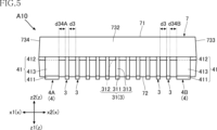
- FIG. 5 is a front view of the electronic device according to the first embodiment.
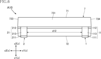
- FIG. 6 is a rear view of the electronic device according to the first embodiment.
- FIG. 7 is a left side view showing the electronic device according to the first embodiment.
- FIG. 8 is a right side view showing the electronic device according to the first embodiment.
- FIG. 9 is a cross-sectional view taken along line IX-IX in FIG.
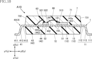
- FIG. 10 is a cross-sectional view taken along line XX in FIG.
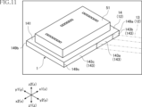
- FIG. 11 is an enlarged perspective view of a main portion showing a first die pad portion and a first electronic component of the electronic device according to the first embodiment.
- FIG. 12 is an enlarged perspective view of a main portion showing a second die pad portion and a second electronic component of the electronic device according to the first embodiment.
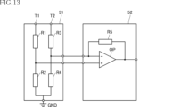
- FIG. 13 is a diagram illustrating a circuit configuration of the first electronic component and the second electronic component of the electronic device according to the first embodiment.
- FIG. 14 is a plan view showing a process for manufacturing the electronic device according to the first embodiment.
- FIG. 15 is a plan view showing an electronic device according to a first modified example of the first embodiment, in which a sealing resin is indicated by imaginary lines.
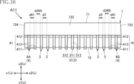
- FIG. 16 is a front view showing an electronic device according to a first modified example of the first embodiment.
- FIG. 16 is a front view showing an electronic device according to a first modified example of the first embodiment.
- FIG. 17 is a rear view showing the electronic device according to the first modified example of the first embodiment.
- FIG. 18 is a plan view showing an electronic device according to a second modified example of the first embodiment, in which the sealing resin is indicated by imaginary lines.
- FIG. 19 is a plan view showing an electronic device according to a third modified example of the first embodiment, in which the sealing resin is indicated by imaginary lines.
- FIG. 20 is a plan view showing an electronic device according to a fourth modified example of the first embodiment, in which the sealing resin is indicated by imaginary lines.
- FIG. 21 is a diagram showing a circuit configuration of a first electronic component and a second electronic component of an electronic device according to a fourth modified example of the first embodiment. In FIG. FIG. FIG.
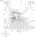
- FIG. 22 is a plan view showing an electronic device according to another configuration of the fourth modified example of the first embodiment, in which the sealing resin is indicated by imaginary lines.
- FIG. 23 is an enlarged plan view of a main part of an electronic device according to the second embodiment.
- FIG. 24 is an enlarged plan view of a main part of an electronic device according to the second embodiment.
- an object A is formed on an object B
- an object A is formed on (an object B)
- an object A is formed directly on an object B
- an object A is formed on an object B with another object interposed between the object A and the object B” unless otherwise specified.
- an object A is disposed on an object B” and “an object A is disposed on (an object B)” include “an object A is disposed directly on an object B” and “an object A is disposed on (an object B) with another object interposed between the object A and the object B” unless otherwise specified.
- an object A is located on (an object B) includes “an object A is in contact with an object B and is located on (an object B)” and “an object A is located on (an object B) with another object interposed between the object A and the object B".
- an object A overlaps an object B includes “an object A overlaps the entire object B” and “an object A overlaps a part of an object B” unless otherwise specified.
- an object A (its material) contains a certain material C includes “an object A (its material) is made of a certain material C” and “an object A (its material) is mainly composed of a certain material C.”
- a certain surface A faces a certain direction B (one side or the other side) includes, unless otherwise specified, the angle of surface A with respect to direction B is not limited to 90°, and includes the case where surface A is inclined with respect to direction B.
- a certain surface A is perpendicular to a certain surface B includes, unless otherwise specified, the angle of surface A with respect to surface B is not limited to 90°, and includes the case where surface A is inclined with respect to surface B.
- the electronic device A10 includes a first lead 1, a second lead 2, a plurality of third leads 3, a pair of fourth leads 4, a first electronic component 51, a second electronic component 52, a plurality of connecting members 61 to 66, and a sealing resin 7.
- the electronic device A10 includes eleven third leads 3, but the number of third leads 3 is not limited in any way.
- the specific use of the electronic device A10 is not limited in any way, but may be, for example, for detecting the battery voltage of an electric vehicle.
- the electronic device A10 does not detect the battery voltage of an electric vehicle, but may detect other voltages of the electric vehicle, or may detect voltages used in industrial equipment, home appliances, power supplies, etc., other than electric vehicles.
- the electronic device A10 is a surface-mounted semiconductor package, and in this embodiment, it is an SOP (Small Outline Package) type, as shown in FIG. 1 and FIG. 5 to FIG. 8.
- the thickness direction z corresponds to the thickness direction of the electronic device A10 (first electronic component 51).
- Planar view refers to the view in the thickness direction z.
- the first direction y is perpendicular to the thickness direction z.
- the second direction x is perpendicular to the thickness direction z and the first direction y.
- One side of the first direction y is referred to as the y1 side of the first direction y, and the other side of the first direction y is referred to as the y2 side of the first direction y.
- One side of the second direction x is referred to as the x1 side of the second direction x, and the other side of the second direction x is referred to as the x2 side of the second direction x.
- One side of the thickness direction z is referred to as the z1 side of the thickness direction z, and the other side of the thickness direction z is referred to as the z2 side of the thickness direction z.
- the z2 side of the thickness direction z is sometimes referred to as the upper side, and the z1 side of the thickness direction z is sometimes referred to as the lower side.
- Terms such as “top,” “bottom,” “upper,” “lower,” “top surface,” and “bottom surface” indicate the relative positional relationship of each part in the thickness direction z, and do not necessarily define the relationship with the direction of gravity.
- the first lead 1, the second lead 2, the multiple third leads 3, and the pair of fourth leads 4 include metals such as Cu (copper), Ni (nickel), Fe (iron), etc.
- the first lead 1, the second lead 2, the multiple third leads 3, and the pair of fourth leads 4 are formed from the same lead frame (lead frame 9 described below).
- the first lead 1, the second lead 2, the multiple third leads 3, and the pair of fourth leads 4 are formed, for example, by subjecting a metal plate material to a process selected from punching, bending, etching, etc.
- a plating layer made of Ag (silver), Ni, Au (gold), etc. may be provided at appropriate locations on each of the first lead 1, the second lead 2, the multiple third leads 3, and the pair of fourth leads 4, as necessary.
- the first lead 1, the second lead 2, the multiple third leads 3, and the pair of fourth leads 4 are electrically connected to the first electronic component 51 or the second electronic component 52, and form a conductive path in the electronic device A10.
- the first lead 1, the second lead 2, the multiple third leads 3, and the pair of fourth leads 4 are spaced apart from each other.
- the first lead 1, the second lead 2, the multiple third leads 3, and the pair of fourth leads 4 each have a portion covered by the sealing resin 7 and a portion exposed from the sealing resin 7.
- the first lead 1 includes a first outer portion 11 and a first inner portion 12.
- the first outer portion 11 and the first inner portion 12 are connected to each other and formed integrally.
- the boundary between the first outer portion 11 and the first inner portion 12 overlaps with the periphery of the sealing resin 7 in a plan view.
- the first outer part 11 is a part of the first lead 1 that is exposed from the sealing resin 7.
- the first outer part 11 protrudes from the sealing resin 7 to the y2 side in the first direction y.
- the first outer part 11 has a rectangular shape with the first direction y as the longitudinal direction in a plan view.
- the first outer part 11 is bent in a gull-wing shape when viewed in the second direction x.
- the dimension W11 (see FIG. 1) of the first outer part 11 along the second direction x is not limited in any way, but is, for example, 0.1 mm or more and 1.5 mm or less.
- the first outer part 11 includes a first mounting part 111, a first root part 112, and a first relay part 113.
- the first mounting portion 111 is the tip portion of the first outer portion 11.
- the first mounting portion 111 is a portion that is joined to the circuit board when the electronic device A10 is mounted on the circuit board. As shown in Figures 1 and 2, the first mounting portion 111 is located at the end opposite the sealing resin 7 in the first direction y. Therefore, the first mounting portion 111 is located farther from the sealing resin 7 in the first direction y than the first root portion 112 and the first relay portion 113. The first mounting portion 111 is located lower in the thickness direction z than the first root portion 112.
- the first root portion 112 is the root portion of the first outer part 11. As shown in Figures 1 and 2, the first root portion 112 is located at the end of the first outer part 11 that is closer to the sealing resin 7 in the first direction y. Therefore, the first root portion 112 is located closer to the sealing resin 7 in the first direction y than the first mounting part 111 and the first relay part 113. The first root portion 112 is located above the first mounting part 111 in the thickness direction z, and protrudes from the center of the sealing resin 7 in the thickness direction z.
- the first relay portion 113 connects the first mounting portion 111 and the first root portion 112.
- the first relay portion 113 is inclined with respect to the first mounting portion 111 and the first root portion 112 when viewed in the second direction x.
- the first relay portion 113 is inclined with respect to the thickness direction z.
- the first inner portion 12 is a portion of the first lead 1 that is covered with the sealing resin 7.
- the first inner portion 12 extends from the first outer portion 11 inwardly into the sealing resin 7.
- the first inner portion 12 includes a first connecting portion 13 and a first die pad portion 14.
- the first connecting portion 13 extends from the first outer portion 11 inwardly into the sealing resin 7.
- the first connecting portion 13 is connected to the first die pad portion 14.
- the first connecting portion 13 connects the first inner portion 12 and the first die pad portion 14.
- the first die pad portion 14 has the first electronic component 51 mounted thereon and supports the first electronic component 51.
- the first connecting portion 13 is connected to the first die pad portion 14, and the first die pad portion 14 is supported by the first connecting portion 13.
- the first die pad portion 14 is located on the y1 side of the first direction y of the first outer portion 11. Therefore, the first outer portion 11 is disposed on the y2 side of the first direction y with respect to the first die pad portion 14.
- the center of the first die pad portion 14 in the second direction x is located on the x2 side of the second direction x from the center of the first outer portion 11 in the second direction x.
- the center of the first outer portion 11 is located on the x1 side of the second direction x from the center of the first die pad portion 14.
- a part of the first root portion 112 overlaps with the first die pad portion 14 when viewed in the first direction y.
- the entire first root portion 112 may overlap the first die pad portion 14 when viewed in the first direction y.
- the entire first root portion 112 may not overlap the first die pad portion 14.
- the first outer portion 11 may be disposed outward (on the x1 side of the second direction x) from the first die pad portion 14 in the second direction x.
- the first die pad portion 14 has a main surface 141, a back surface 142, and a first side surface 143.
- the main surface 141 and the back surface 142 are spaced apart in the thickness direction z.
- the main surface 141 faces upward in the thickness direction z
- the back surface 142 faces downward in the thickness direction z.
- the first side surface 143 is connected to the main surface 141 and the back surface 142.
- the first side surface 143 faces in the first direction y toward the side where the first outer part 11 is located (the y2 side in the first direction y).
- the first connecting part 13 is connected to the first side surface 143.
- the inclination angle ⁇ 1 of the first connecting part 13 with respect to the first side surface 143 is not limited in any way, but is, for example, 10° or more and 89° or less, and in this embodiment, the inclination angle ⁇ 1 is 45°.
- the first side surface 143 includes a connecting region 143a and a pair of side regions 143b, 143c.
- the connecting region 143a is a region of the first side surface 143 that is connected to the first connecting portion 13.
- the connecting region 143a is in contact with the first connecting portion 13.
- the pair of side regions 143b, 143c are individually arranged on both sides of the connecting region 143a in the second direction x.
- the side region 143b is located on the x1 side of the second direction x with respect to the connecting region 143a, and the side region 143c is located on the x2 side of the second direction x (the same side as the second lead 2) with respect to the connecting region 143a.
- the pair of side regions 143b, 143c are each in contact with the sealing resin 7.
- the connecting region 143a is disposed on the x1 side of the first side surface 143 in the second direction x from the center in the second direction x. Therefore, the dimension in the second direction x of the lateral region 143b is smaller than the dimension in the second direction x of the lateral region 143c.
- the connecting region 143a may be disposed on the x2 side of the first side surface 143 in the second direction x from the center in the second direction x.
- the dimension in the second direction x of the lateral region 143b may be the same as the dimension in the second direction x of the lateral region 143c, or may be larger than the dimension in the second direction x of the lateral region 143c.
- the shape of the first die pad portion 14 in a plan view is rectangular.
- the first die pad portion 14 has a first corner portion 149a, a second corner portion 149b, and two other corner portions 149c and 149d.
- the first corner 149a is located on the y2 side in the first direction y and the x1 side in the second direction x of the four corners of the first die pad portion 14 in a planar view.
- the first corner 149a is closest to the first outer portion 11 of the four corners of the first die pad portion 14.
- the second corner 149b is located on the y1 side in the first direction y and the x2 side in the second direction x of the four corners of the first die pad portion 14 in a planar view.
- the second corner 149b is diagonal to the first corner 149a.
- the second corner 149b is farthest from the first outer portion 11 of the four corners of the first die pad portion 14.
- the corner 149c is located on the y2 side in the first direction y and the x2 side in the second direction x of the four corners of the first die pad portion 14 in a planar view.
- the corner 149d is located on the y1 side in the first direction y and on the x1 side in the second direction x.
- the corner 149d is diagonal to the corner 149c.
- the first corner 149a and the corner 149c are both ends of the first side surface 143 in the second direction x.
- the second lead 2 includes a second outer portion 21 and a second inner portion 22.
- the second outer portion 21 and the second inner portion 22 are connected to each other and formed integrally.
- the boundary between the second outer portion 21 and the second inner portion 22 overlaps with the periphery of the sealing resin 7 in a plan view.
- the second outer part 21 is a portion of the second lead 2 that is exposed from the sealing resin 7.
- the second outer part 21 protrudes from the sealing resin 7 to the y2 side in the first direction y (the same side as the first outer part 11).
- the second outer part 21 has a rectangular shape with the first direction y as its longitudinal direction.
- the plan view shape of the second outer part 21 is congruent with the plan view shape of the first outer part 11, but unlike this configuration, these plan view shapes do not have to be congruent with each other.
- the second outer part 21 is bent in a gull-wing shape when viewed in the second direction x.
- the second outer part 21 overlaps the first outer part 11 when viewed in the second direction x.
- the dimension W21 (see FIG.
- the dimension W21 of the second outer part 21 is not limited in any way and is, for example, 0.1 mm or more and 1.5 mm or less.
- the dimension W21 of the second outer part 21 is the same as the dimension W11 of the first outer part 11, but in some configurations, the dimension W21 and the dimension W11 may be different.
- the second outer part 21 includes a second mounting part 211, a second root part 212, and a second relay part 213.
- the second mounting portion 211 is the tip portion of the second outer portion 21.
- the second mounting portion 211 is a portion that is joined to the circuit board when the electronic device A10 is mounted on the circuit board. As shown in Figures 1 and 2, the second mounting portion 211 is located at the end opposite the sealing resin 7 in the first direction y. Therefore, the second mounting portion 211 is located farther from the sealing resin 7 in the first direction y than the second root portion 212 and the second relay portion 213.
- the second mounting portion 211 is located lower in the thickness direction z than the second root portion 212.
- the second mounting portion 211 is disposed at the same position as the first mounting portion 111 in the thickness direction z.
- the second root portion 212 is the root portion of the second outer part 21. As shown in Figures 1 and 2, the second root portion 212 is located at the end of the second outer part 21 on the sealing resin 7 side in the first direction y. Therefore, the second root portion 212 is located closer to the sealing resin 7 than the second mounting part 211 and the second relay part 213 in the first direction y. The second root portion 212 is located above the second mounting part 211 in the thickness direction z, and protrudes from the center of the sealing resin 7 in the thickness direction z. The second root portion 212 is located at the same position as the first root portion 112 in the thickness direction z.
- the second relay portion 213 connects the second mounting portion 211 and the second root portion 212.
- the second relay portion 213 is inclined with respect to the first mounting portion 111 and the first root portion 112 when viewed in the second direction x.
- the second relay portion 213 is inclined with respect to the thickness direction z.
- the second inner portion 22 is a portion of the second lead 2 that is covered with the sealing resin 7.
- the second inner portion 22 is connected to the second outer portion 21 and extends from the second outer portion 21 inwardly into the sealing resin 7.
- the second inner portion 22 extends from the second outer portion 21 inwardly into the sealing resin 7 so as to approach the first die pad portion 14.
- Each of the multiple third leads 3 includes a third outer portion 31 and a third inner portion 32.
- the electronic device A10 has multiple third outer portions 31 and multiple third inner portions 32.
- the third outer portion 31 and the third inner portion 32 are connected to each other and formed integrally.
- the boundary between the third outer portion 31 and the third inner portion 32 overlaps the periphery of the sealing resin 7 in a plan view.
- the third outer portion 31 and the third inner portion 32 described below are common to each third lead 3 unless otherwise specified.
- the third outer portion 31 is a portion of each third lead 3 that is exposed from the sealing resin 7. Each third outer portion 31 protrudes from the sealing resin 7 to the y1 side of the first direction y (the opposite side to the first outer portion 11 and the second outer portion 21). In a plan view, each third outer portion 31 is in the shape of a strip with the first direction y as its longitudinal direction. The multiple third outer portions 31 are arranged at equal intervals along the second direction x. Each third outer portion 31 is bent in a gull-wing shape when viewed in the second direction x. The multiple third outer portions 31 overlap each other when viewed in the second direction x.
- the dimension W31 (see FIG.
- the third outer portion 31 along the second direction x is not limited in any way, but is, for example, 0.15 mm or more and 0.5 mm or less.
- the dimension W31 of the third outer portion 31 is smaller than the dimension W11 of the first outer portion 11 and the dimension W21 of the second outer portion 21.
- the third outer part 31 includes a third mounting part 311, a third root part 312, and a third relay part 313.
- the electronic device A10 has a plurality of third mounting parts 311, a plurality of third root parts 312, and a plurality of third relay parts 313.
- the third mounting parts 311, the third root parts 312, and the third relay parts 313 described below are common to each third outer part 31 unless otherwise specified.
- the third mounting portion 311 is the tip portion of the third outer portion 31.
- the third mounting portion 311 is a portion that is joined to the circuit board when the electronic device A10 is mounted on the circuit board. As shown in FIG. 1 and FIG. 2, the third mounting portion 311 is located at the end opposite the sealing resin 7 in the first direction y. Therefore, the third mounting portion 311 is located farther from the sealing resin 7 in the first direction y than the third root portion 312 and the third relay portion 313.
- the third mounting portion 311 is located lower in the thickness direction z than the third root portion 312.
- the multiple third mounting portions 311 are arranged at the same position in the thickness direction z.
- the multiple third mounting portions 311 are arranged at equal intervals along the second direction x.
- the third root portion 312 is a root portion of the third outer part 31. As shown in Figures 1 and 2, the third root portion 312 is located at the end of the third outer part 31 on the sealing resin 7 side in the first direction y. Therefore, the third root portion 312 is located closer to the sealing resin 7 than the third mounting part 311 and the third relay part 313 in the first direction y. The third root portion 312 is located above the third mounting part 311 in the thickness direction z, and protrudes from the center of the sealing resin 7 in the thickness direction z. The multiple third root portions 312 are arranged at the same positions as each other in the thickness direction z.
- the third relay portion 313 connects the third mounting portion 311 and the third root portion 312.
- the third relay portion 313 is inclined with respect to the third mounting portion 311 and the third root portion 312 when viewed in the second direction x.
- the third relay portion 313 is inclined with respect to the thickness direction z.
- the third inner portion 32 is a portion of each third lead 3 that is covered with the sealing resin 7.
- the third inner portion 32 is connected to the third outer portion 31 and extends from the third outer portion 31 inwardly into the sealing resin 7.
- the third inner portion 32 extends from the third outer portion 31 inwardly into the sealing resin 7 so as to approach a portion of the fourth lead 4A (second die pad portion 44) described below.
- the pair of fourth leads 4 are arranged on both sides of the multiple third leads 3 in the second direction x.
- one of the pair of fourth leads 4 may be referred to as the "fourth lead 4A” and the other of the pair of fourth leads 4 may be referred to as the "fourth lead 4B".
- the fourth lead 4A is arranged on the x1 side of the second direction x with respect to the multiple third leads 3, and the fourth lead 4B is arranged on the x2 side of the second direction x with respect to the multiple third leads 3.
- the planar shape of the fourth lead 4A is congruent with the planar shape of the first lead 1, but they do not have to be congruent.
- the planar shape of the fourth lead 4B is congruent with the planar shape of the second lead 2, but they do not have to be congruent.
- Each of the pair of fourth leads 4 includes a fourth outer portion 41 and a fourth inner portion 42.
- the fourth outer portion 41 and the fourth inner portion 42 are connected to each other and formed integrally.
- the boundary between the fourth outer portion 41 and the fourth inner portion 42 overlaps the periphery of the sealing resin 7 in a plan view.
- the fourth outer portion 41 and the fourth inner portion 42 described below are common to each fourth lead 4 unless otherwise specified.
- the fourth outer portion 41 is a portion of the fourth lead 4 that is exposed from the sealing resin 7.
- the fourth outer portion 41 protrudes from the sealing resin 7 to the other side in the first direction y.
- the fourth outer portion 41 of the fourth lead 4A is located on the x1 side in the second direction x relative to the multiple third outer portions 31, and the fourth outer portion 41 of the fourth lead 4B is located on the x2 side in the second direction x relative to the multiple third outer portions 31.
- the fourth outer portion 41 is bent in a gull-wing shape when viewed in the second direction x.
- the fourth outer portion 41 overlaps each of the third outer portions 31 when viewed in the second direction x.
- the fourth outer portion 41 is rectangular in plan view with the first direction y as its longitudinal direction.
- the plan view shape of the fourth outer portion 41 is congruent with the plan view shape of the first outer portion 11, but unlike this configuration, these plan view shapes do not have to be congruent with each other.
- the fourth outer portion 41 of the fourth lead 4A overlaps the first outer portion 11 when viewed in the first direction y
- the fourth outer portion 41 of the fourth lead 4B overlaps the second outer portion 21 when viewed in the first direction y.
- the dimension W41 (see FIG. 1 ) of the fourth outer portion 41 along the second direction x is not limited in any way, but is, for example, 0.1 mm or more and 1.5 mm or less.
- the dimension W41 of the fourth outer portion 41 is the same as the dimension W11 of the first outer portion 11 and the dimension W21 of the second outer portion 21, but unlike this configuration, the dimension W41 of the fourth outer portion 41 may be different from the dimension W11 of the first outer portion 11 and the dimension W21 of the second outer portion 21.
- the fourth outer portion 41 includes a fourth mounting portion 411, a fourth root portion 412, and a fourth relay portion 413.
- the fourth mounting portion 411, fourth root portion 412, and fourth relay portion 413 described below are common to the fourth outer portion 41 of each fourth lead 4 unless otherwise specified.
- the fourth mounting portion 411 is the tip portion of the fourth outer portion 41.
- the fourth mounting portion 411 is a portion that is joined to the circuit board when the electronic device A10 is mounted on the circuit board. As shown in Figures 1 and 2, the fourth mounting portion 411 is located at the end opposite the sealing resin 7 in the first direction y. Therefore, the fourth mounting portion 411 is located farther from the sealing resin 7 in the first direction y than the fourth root portion 412 and the fourth relay portion 413.
- the fourth mounting portion 411 is located lower in the thickness direction z than the fourth root portion 412.
- the fourth mounting portion 411 is located at the same position as each third mounting portion 311 in the thickness direction z.
- the fourth mounting portion 411 of the fourth lead 4A is adjacent to the second direction x on the x1 side of the second direction x of the multiple third mounting portions 311.
- the fourth mounting portion 411 of the fourth lead 4B is adjacent to the third mounting portions 311 on the x2 side in the second direction x.
- the fourth mounting portion 411 of the fourth lead 4A overlaps the first mounting portion 111 of the first lead 1 when viewed in the first direction y.
- the fourth mounting portion 411 of the fourth lead 4B overlaps the second mounting portion 211 of the second lead 2 when viewed in the first direction y.
- the fourth root portion 412 is the root portion of the fourth outer part 41. As shown in Figures 1 and 2, the fourth root portion 412 is located at the end of the fourth outer part 41 on the sealing resin 7 side in the first direction y. Therefore, the fourth root portion 412 is located closer to the sealing resin 7 in the first direction y than the fourth mounting part 411 and the fourth relay part 413. The fourth root portion 412 is located above the fourth mounting part 411 in the thickness direction z, and protrudes from the center of the sealing resin 7 in the thickness direction z. The fourth root portion 412 is located at the same position as each third root portion 312 in the thickness direction z.
- the fourth relay portion 413 connects the fourth mounting portion 411 and the fourth root portion 412.
- the fourth relay portion 413 is inclined with respect to the fourth mounting portion 411 and the fourth root portion 412 when viewed in the second direction x.
- the fourth relay portion 413 is inclined with respect to the thickness direction z.
- the fourth inner portion 42 is a portion of the corresponding fourth lead 4 that is covered with the sealing resin 7.
- the fourth inner portion 42 is connected to the fourth outer portion 41 and extends from the fourth outer portion 41 inwardly into the sealing resin 7.
- the fourth inner portion 42 of the fourth lead 4B extends from the fourth outer portion 41 inwardly into the sealing resin 7 so as to approach the second die pad portion 44.
- the fourth inner portion 42 of the fourth lead 4A includes the second connecting portion 43 and the second die pad portion 44.
- the second connecting portion 43 extends from the fourth outer portion 41 inwardly into the sealing resin 7.
- the second connecting portion 43 is connected to the second die pad portion 44.
- the second connecting portion 43 connects the fourth outer portion 41 and the second die pad portion 44.
- the second die pad portion 44 has the second electronic component 52 mounted thereon and supports the second electronic component 52.
- the second connecting portion 43 is connected to the second die pad portion 44, and the second die pad portion 44 is supported by the second connecting portion 43.
- the second die pad portion 44 is spaced apart from the first die pad portion 14.
- the first die pad portion 14 and the second die pad portion 44 are aligned in the first direction y, and the second die pad portion 44 is located on the y1 side of the first direction y from the first die pad portion 14.
- the second die pad portion 44 is located on the y2 side of the first direction y from the fourth outer portion 41. Therefore, the fourth outer portion 41 is disposed on the y1 side of the first direction y from the second die pad portion 44.
- the center in the second direction x of the second die pad portion 44 is located on the x2 side of the second direction x from the center in the second direction x of the fourth outer portion 41 of the fourth lead 4A. Therefore, in the second direction x, the center of the fourth outer portion 41 of the fourth lead 4A is located on the x1 side of the center of the second die pad portion 44 in the second direction x.
- a part of the fourth root portion 412 of the fourth lead 4A overlaps with the second die pad portion 44 when viewed in the first direction y.
- the entire fourth root portion 412 of the fourth lead 4A may overlap with the second die pad portion 44 when viewed in the first direction y.
- the entire fourth root portion 412 of the fourth lead 4A may not overlap with the second die pad portion 44. Therefore, in the fourth lead 4A, the fourth outer portion 41 may be disposed outward (on the x1 side of the second direction x) from the second die pad portion 44 in the second direction x.
- the second die pad portion 44 has a main surface 441, a back surface 442, and a second side surface 443.
- the main surface 441 and the back surface 442 are spaced apart in the thickness direction z.
- the main surface 441 faces upward in the thickness direction z
- the back surface 442 faces downward in the thickness direction z.
- the second side surface 443 is connected to the main surface 441 and the back surface 442.
- the second side surface 443 faces in the first direction y toward the side where the fourth outer part 41 of the fourth lead 4A is located (the y1 side in the first direction y).
- the second connecting part 43 is connected to the second side surface 443.
- the inclination angle ⁇ 1 of the second connecting part 43 with respect to the second side surface 443 is not limited in any way, but is, for example, 10° or more and 89° or less, and in this embodiment, the inclination angle ⁇ 1 is 45°.
- the second side surface 443 includes a connecting region 443a and a pair of side regions 443b, 443c.
- the connecting region 443a is a region of the second side surface 443 that is connected to the second connecting portion 43.
- the connecting region 443a is in contact with the second connecting portion 43.
- the pair of side regions 443b, 443c are individually arranged on both sides of the connecting region 443a in the second direction x.
- the side region 443b is located on the x1 side of the second direction x with respect to the connecting region 443a, and the side region 443c is located on the x2 side of the second direction x with respect to the connecting region 443a (the same side as the fourth lead 4B).
- the pair of side regions 443b, 443c are each in contact with the sealing resin 7.
- the connecting region 443a is disposed on the x1 side of the second direction x from the center in the second direction x of the second side 443. Therefore, the dimension in the second direction x of the lateral region 443b is smaller than the dimension in the second direction x of the lateral region 443c. Unlike this configuration, the connecting region 443a may be disposed on the x2 side of the second direction x from the center in the second direction x of the second side 443. In other words, the dimension in the second direction x of the lateral region 443b may be the same as the dimension in the second direction x of the lateral region 443c, or may be larger than the dimension in the second direction x of the lateral region 443c.
- the shape of the second die pad portion 44 in a plan view is rectangular.
- the second die pad portion 44 has four corners 449a, 449b, 449c, and 449d.
- corner 449a is located on the y1 side in the first direction y and the x1 side in the second direction x among the four corners of the second die pad portion 44 in a planar view. Corner 449a is closest to the fourth outer portion 41 of the fourth lead 4A among the four corners of the second die pad portion 44 in a planar view. Corner 449b is located on the y2 side in the first direction y and the x2 side in the second direction x among the four corners of the second die pad portion 44 in a planar view. Corner 449b is diagonal to corner 449a. Corner 449b is farthest from the fourth outer portion 41 of the fourth lead 4A among the four corners of the second die pad portion 44.
- Corner 449c is located on the y1 side in the first direction y and the x2 side in the second direction x among the four corners of the second die pad portion 44 in a planar view.
- the corner 449d is located on the y2 side in the first direction y and on the x1 side in the second direction x.
- the corner 449d is diagonal to the corner 449c.
- the corners 449a and 449c are both ends of the second side surface 443 in the second direction x.
- the first outer part 11 and the first inner part 12 are adjacent to each other with a distance d12 (see FIG. 6) in the second direction x.
- the multiple third outer parts 31 are arranged with an arrangement distance d3 (see FIG. 5) in the second direction x.
- the distance d12 (see FIG. 6) in the second direction x between the first outer part 11 and the first inner part 12 is larger than the arrangement distance d3 (see FIG. 5) in the second direction x between the third outer parts 31 adjacent to each other in the second direction x.
- the distance d12 is 10 times or more and 20 times or less than the arrangement distance d3.
- the distance d12 is, for example, 5 mm or more and 10 mm or less
- the arrangement distance d3 is, for example, 0.25 mm or more and 5 mm or less.
- the distance d12 is preferably 4 mm or more to prevent a short circuit between the first outer part 11 and the second outer part 21.
- the distance d34A (see FIG. 5) in the second direction x between the fourth outer part 41 of the fourth lead 4A and the third outer part 31 adjacent to the fourth outer part 41, and the distance d34B (see FIG. 5) in the second direction x between the fourth outer part 41 of the fourth lead 4B and the third outer part 31 adjacent to the fourth outer part 41 are the same as the arrangement distance d3.
- the shapes and positional relationships between each of the first die pad portion 14 and the second die pad portion 44 and each of the first inner portion 12, the second inner portion 22, each of the third inner portions 32, and each of the fourth inner portions 42 are not limited to the example shown in the figure, and can be changed as appropriate depending on the specifications of electronic device A10.
- the first electronic component 51 and the second electronic component 52 are elements that perform electrical functions in the electronic device A10.
- the specific functions of the first electronic component 51 and the second electronic component 52 are not limited in any way, but in this embodiment, the first electronic component 51 and the second electronic component 52 have the function of detecting voltage.
- the first electronic component 51 is bonded to the first die pad portion 14 by a bonding material (such as solder or sintered silver) not shown, and is mounted on the first die pad portion 14.
- a bonding material such as solder or sintered silver
- the first electronic component 51 and the connection region 143a of the first die pad portion 14 are arranged along the first direction y in a plan view.
- the first electronic component 51 outputs a first signal corresponding to the potential of the first lead 1 and a second signal corresponding to the potential of the second lead 2 to the second electronic component 52.
- the first electronic component 51 has a plurality of electrodes 511, 512, 513 arranged on the upper surface in the thickness direction z.
- the second electronic component 52 is bonded to the second die pad portion 44 by a bonding material (such as solder or sintered silver) not shown, and is mounted on the second die pad portion 44.
- the second electronic component 52 and the connection region 443a of the second die pad portion 44 are arranged along the first direction y in a plan view.
- the second electronic component 52 receives the first signal and the second signal from the first electronic component 51, and outputs a third signal according to the potential difference between the first lead 1 and the second lead 2.
- the second electronic component 52 outputs a detection signal (third signal) of the voltage applied between the first lead 1 and the second lead 2.
- the second electronic component 52 has a plurality of electrodes 521, 522 arranged on the upper surface in the thickness direction z.
- the first electronic component 51 and the second electronic component 52 have a circuit configuration, for example, as shown in FIG. 13.
- the first electronic component 51 includes a plurality of resistive elements R1 to R4, and the second electronic component 52 includes an operational amplifier OP and a resistive element R5.
- the circuit configuration of the first electronic component 51 and the second electronic component 52 is not limited to the example shown in FIG. 13.
- the two resistive elements R1 and R2 are connected in series with each other.
- the two resistive elements R1 and R2 divide the voltage of terminal T1 (the potential difference between the potential of terminal T1 and the reference potential of ground GND).
- terminal T1 corresponds to multiple electrodes 512.
- the connection point of the two resistive elements R1 and R2 is connected to the non-inverting input terminal of the operational amplifier OP.
- the two resistive elements R3 and R4 are connected in series with each other.
- the two resistive elements R3 and R4 divide the voltage of terminal T2 (the potential difference between the potential of terminal T2 and the reference potential of ground GND).
- terminal T2 corresponds to multiple electrodes 511.
- connection point of the two resistive elements R3 and R4 is connected to the inverting input terminal of the operational amplifier OP.
- electronic device A10 detects the voltage of a battery installed in an electric vehicle, one of terminals T1 and T2 is electrically connected to the high-potential terminal of the battery, and the other is electrically connected to the low-potential terminal.
- the operational amplifier OP receives a first signal (in this embodiment, a signal obtained by dividing the voltage at terminal T1) corresponding to the potential at terminal T1 and a second signal (in this embodiment, a signal obtained by dividing the voltage at terminal T2) corresponding to the potential at terminal T2, and outputs a third signal corresponding to the potential difference between terminals T1 and T2.
- the resistive element R5 is an element (feedback resistor) for determining the amplification gain of the operational amplifier OP, and one end of the resistive element R5 is connected to the inverting input terminal of the operational amplifier OP, and the other end is connected to the output terminal of the operational amplifier OP.
- the second electronic component 52 does not need to include the resistive element R5.
- the multiple connection members 61-66 each electrically connect parts spaced apart from one another.
- the multiple connection members 61-66 are each bonding wires.
- the multiple connection members 61-66 may each be a plate-shaped metal member rather than a bonding wire.
- the multiple connection members 61-66 each contain Au, Al (aluminum), or Cu.
- connection member 61 is joined to the electrode 511 of the first electronic component 51 and the second inner portion 22, and electrically connects the first electronic component 51 and the second lead 2. Therefore, the second outer portion 21 of the second lead 2 is electrically connected to the first electronic component 51 via the second inner portion 22 and the connection member 61.
- connection member 62 is joined to the electrode 512 of the first electronic component 51 and the first connecting portion 13 (first inner portion 12), electrically connecting the first electronic component 51 and the first lead 1. Therefore, the first outer portion 11 of the first lead 1 is electrically connected to the first electronic component 51 via the first connecting portion 13 and the connection member 62.
- each of the multiple connection members 63 is joined to the electrode 521 of the second electronic component 52 and one of the multiple third inner parts 32, electrically connecting the second electronic component 52 to one of the multiple third leads 3. Therefore, each third outer part 31 of the multiple third leads 3 is electrically connected to the second electronic component 52 via the corresponding third inner part 32 and the corresponding connection member 63.
- connection member 64 is joined to the electrode 521 of the second electronic component 52 and the fourth inner portion 42 of the fourth lead 4B, electrically connecting the second electronic component 52 and the fourth lead 4B. Therefore, the fourth outer portion 41 of the fourth lead 4B is electrically connected to the second electronic component 52 via the fourth inner portion 42 of the fourth lead 4B and the connection member 64.
- connection member 65 is joined to the electrode 521 of the second electronic component 52 and the second coupling portion 43 (fourth inner portion 42), electrically connecting the second electronic component 52 and the fourth lead 4A.
- the fourth outer portion 41 of the fourth lead 4A is electrically connected to the second electronic component 52 via the second coupling portion 43 of the fourth lead 4A and the connection member 65.
- the multiple connection members 66 are joined to the electrodes 513 of the first electronic component 51 and the electrodes 522 of the second electronic component 52, electrically connecting the first electronic component 51 and the second electronic component 52.
- the multiple connection members 66 are transmission paths for the first signal and the second signal.
- the sealing resin 7 covers the first lead 1, the second lead 2, the plurality of third leads 3, and a portion of each of the pair of fourth leads 4, the first electronic component 51, the second electronic component 52, and the plurality of connection members 61 to 66.
- the sealing resin 7 includes an insulating material such as an epoxy resin.
- the sealing resin 7 is made of a resin material having a CTI (Comparative Tracking Index) of 600 V or more.
- the method of forming the sealing resin 7 is not limited, but may be, for example, molding.
- the sealing resin 7 has, for example, a rectangular parallelepiped shape.
- the sealing resin 7 has a dimension along the second direction x of, for example, 5 mm or more and 10 mm or less, and a dimension along the first direction y of, for example, 3 mm or more and 13 mm or less.
- the sealing resin 7 has a resin main surface 71, a resin back surface 72, a first resin side surface 731, a second resin side surface 732, and two resin side surfaces 733 and 734.
- the resin main surface 71 and the resin back surface 72 are spaced apart from each other in the thickness direction z.
- the resin main surface 71 faces the z2 side in the thickness direction z
- the resin back surface 72 faces the z1 side in the thickness direction z.
- the resin main surface 71 is the upper surface of the sealing resin 7, and the resin back surface 72 is the lower surface of the sealing resin 7.
- the first resin side surface 731 and the second resin side surface 732 are spaced apart from each other in the first direction y.
- the first resin side surface 731 faces the y2 side of the first direction y
- the second resin side surface 732 faces the y1 side of the first direction y.
- the two resin side surfaces 733, 734 are spaced apart from each other in the second direction x.
- the resin side surface 733 faces the x2 side of the second direction x
- the resin side surface 734 faces the x1 side of the second direction x.
- the first outer portion 11 and the second outer portion 21 each protrude from the first resin side surface 731.
- each third outer portion 31 of the multiple third leads 3 and each fourth outer portion 41 of the pair of fourth leads 4 each protrude from the second resin side surface 732.
- the sum of the distance d11 (see FIG. 3) from the first connection point 191 to the second connection point 192 and the distance d12 (see FIG. 3) from the second connection point 192 to the second corner 149b is shorter than in the case of the following configuration.
- the first connection portion 13 is connected to the first corner 149a (the corner closest to the first outer portion 11) of the four corners of the first die pad portion 14.
- the first connection point 191 is the center of the boundary between the first inner portion 12 and the first outer portion 11 (hereinafter referred to as the "first boundary").
- the first boundary is a line segment along the second direction x as shown in FIG.
- the center of the first boundary is the center of the line segment in the second direction x.
- the second connection point 192 is the center of the boundary (hereinafter referred to as the "second boundary") between the first connection portion 13 and the first die pad portion 14.
- the second boundary is a line segment along the second direction x as shown in FIG. 3, and the center of the second boundary is the center of the line segment in the second direction x.
- the distance d11 is the shortest distance from the first connection point 191 to the second connection point 192 that passes over the first connection portion 13
- the distance d12 is the shortest distance from the second connection point 192 to the second corner portion 149b that passes over the first die pad portion 14.
- the sum of the distance d21 (see FIG. 4) from the connection point 491 to the connection point 492 and the distance d22 (see FIG. 4) from the connection point 492 to the corner 449b is shorter than in the case of the following configuration.
- the second connection portion 43 is connected to the corner 449a (the corner closest to the fourth outer portion 41 of the fourth lead 4A) among the four corners of the second die pad portion 44.
- the connection point 491 is the center of the boundary (hereinafter referred to as the "third boundary") between the fourth inner portion 42 of the fourth lead 4A and the fourth outer portion 41 of the fourth lead 4A.
- the third boundary is a line segment along the second direction x as shown in FIG. 4, and the center of the third boundary is the center of the line segment in the second direction x.
- the connection point 492 is the center of the boundary (hereinafter referred to as the "fourth boundary") between the second connection portion 43 and the second die pad portion 44.
- the fourth boundary is a line segment along the second direction x as shown in FIG. 4, and the center of the fourth boundary is the center of the line segment in the second direction x.
- the distance d21 is the shortest distance from the connection point 491 to the connection point 492 that passes through the second connection portion 43
- the distance d22 is the shortest distance from the connection point 492 to the corner portion 449b that passes through the second die pad portion 44.
- FIG. 14 shows a process in the manufacture of the electronic device A10.
- FIG. 14 shows the state before the sealing resin 7 is formed.
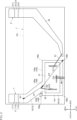
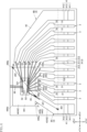
- the first lead 1, the second lead 2, the multiple third leads 3, and the pair of fourth leads 4 are connected to each other by a tie bar 91 and are included in one lead frame 9.
- this tie bar 91 is connected to the first outer part 11 of the first lead 1, the second outer part 21 of the second lead 2, each third outer part 31 of the multiple third leads 3, and each fourth outer part 41 of the pair of fourth leads 4.
- the first inner part 12 is supported by the tie bar 91 at the connection point C1 shown in FIG. 14.
- the fourth inner part 42 of the fourth lead 4A is supported by the tie bar 91 at the connection point C2 shown in FIG. 14.
- the first electronic component 51 and the second electronic component 52 are mounted (joined) on the lead frame 9 shown in FIG. 14, and the connection members 61-66 are formed (wire bonded) and then the sealing resin 7 is formed, for example, by molding.
- the first lead 1, the second lead 2, the multiple third leads 3, and the pair of fourth leads 4 are each cut off from the tie bar 91, and the first outer part 11, the second outer part 21, the third outer parts 31, and the fourth outer parts 41 are each bent to manufacture electronic device A10.
- the center of the first outer part 11 is disposed on the x1 side of the center of the first die pad part 14 in the second direction x.
- the first outer part 11 is shifted from the first die pad part 14 in both directions in the second direction x.
- the connection position of the first connecting part 13 to the first die pad part 14 will be farther away from the center of the first die pad part 14.
- the first side surface 143 includes a connecting region 143a connected to the first connecting part 13, and a pair of side regions 143b, 143c disposed on both sides of the connecting region 143a in the second direction x.
- the connection position of the first connecting portion 13 to the first die pad portion 14 is closer to the center in the second direction x than to the edge of the first die pad portion 14 in the second direction x, so the connection position is closer to the center of the first die pad portion 14. Therefore, in the electronic device A10, the weight of the first die pad portion 14 can reduce the stress applied to the connection portion between the first connecting portion 13 and the first die pad portion 14. In other words, the electronic device A10 can reduce deformation of the first lead 1, i.e., deformation of the lead frame.
- the second side surface 443 includes a connection region 443a connected to the second connecting portion 43 and a pair of side regions 443b, 443c arranged on either side of the connection region 443a in the second direction x, so that the connection position of the second connecting portion 43 to the second die pad portion 44 approaches the center of the second die pad portion 44.
- the weight of the second die pad portion 44 can reduce the stress applied to the connection portion between the second connecting portion 43 and the second die pad portion 44, so that deformation of the fourth lead 4A, i.e., deformation of the lead frame, can be reduced.
- the sum of the distance d11 and the distance d12 is smaller than in a configuration in which the first connecting portion 13 is connected to the first corner 149a (the corner closest to the first outer portion 11) of the four corners of the first die pad portion 14.
- This configuration can reduce deformation of the first lead 1.
- the first inner portion 12 is supported by the tie bar 91 at the connection point C1. In this configuration, a bending moment occurs at the connection point C1 due to an external force applied to the first die pad portion 14.
- the external force is applied to the first die pad portion 14, for example, during the manufacturing process of the electronic device A10, when the lead frame 9 is transported, when the first electronic component 51 is joined to the first die pad portion 14, and when the connection members 61 and 62 are bonded to the first electronic component 51.
- the sum of distance d11 and distance d12 is smaller than in a configuration in which first connecting portion 13 is connected to first corner 149a (the corner closest to first outer portion 11) of the four corners of first die pad portion 14. In other words, electronic device A10 can reduce the bending moment acting on connection point C1, thereby reducing deformation of first lead 1.
- the electronic device A10 can reduce the bending moment applied to the connection point C2, thereby reducing deformation of the fourth lead 4A.
- the side of the first die pad portion 14 is in contact with the sealing resin 7, except for the connecting region 143a.
- the side of the first die pad portion 14 is the surface of the first die pad portion 14 that is connected to the main surface 141 and the back surface 142 and is sandwiched between them, and a part of it is the first side surface 143.
- the inclination angle ⁇ 1 of the first connecting portion 13 relative to the first side surface 143 is 10° or more and 89° or less.
- the first connecting portion 13 is connected to the first side surface 143 at an acute angle. This reduces the strength at the second boundary, increasing the possibility of deformation at the second boundary.
- the second boundary approaches the first corner portion 149a. This increases the sum of the distance d11 and the distance d12, increasing the possibility of deformation at the connection point C1.
- the electronic device A10 can appropriately reduce deformation at the second boundary and deformation at the connection point C1, which is preferable for reducing deformation of the first lead 1.
- the inclination angle ⁇ 1 to 45°, deformation at the second boundary and deformation at the connection point C1 are suppressed in a balanced manner, which is even more preferable in reducing deformation of the first lead 1.
- the inclination angle ⁇ 1 of the second connecting portion 43 relative to the second side surface 443 is greater than or equal to 10° and less than or equal to 89°, which is preferable in terms of reducing deformation of the fourth lead 4A because it is possible to appropriately reduce deformation at the fourth boundary and at the connection point C2.
- the inclination angle ⁇ 1 to 45°, deformation at the fourth boundary and at the connection point C2 are reduced in a balanced manner, which is even more preferable in terms of reducing deformation of the fourth lead 4A.
- connecting region 143a is disposed on the x1 side in the second direction x (i.e., the side where the center in the second direction x of first outer part 11 is located and where first corner part 149a is located) of first side surface 143 from the center in the second direction x.
- This configuration is preferable for setting inclination angle ⁇ 1 of first connecting part 13 with respect to first side surface 143 to be 30° or more and 45° or less.
- connection region 443a is disposed on the second side surface 443, on the x1 side in the second direction x from the center in the second direction x (i.e., the side where the center in the second direction x of the fourth outer portion 41 of the fourth lead 4A is located, and where the corner portion 449a is located).
- This configuration is preferable for making the inclination angle ⁇ 1 of the second connection portion 43 with respect to the second side surface 443 greater than or equal to 30° and less than or equal to 45°.
- this is preferable for ensuring an area in which multiple third leads 3 can be disposed between a pair of fourth leads 4.
- the first outer part 11 and the second outer part 21 are adjacent to each other in the second direction x with a distance d12 therebetween, and the multiple third outer parts 31 are arranged with a spacing d3 therebetween in the second direction x.
- the spacing d12 is greater than the spacing d3.
- the electronic device A10 it is possible to reduce discharge between the first outer part 11 and the second outer part 21 while miniaturizing the device.
- the electronic device A10 has a package structure that is favorable for reducing discharge between the first outer part 11 and the second outer part 21.
- FIGS. 15 to 17 show an electronic device A11 according to a first modified example of the first embodiment.
- the electronic device A11 differs from the electronic device A10 in the following respects. That is, the configurations of the first lead 1, the second lead 2, and the pair of fourth leads 4 are different.
- the first lead 1 of the electronic device A11 includes two first outer parts 11 that are separated from each other. Unlike the illustrated example, the number of the first outer parts 11 may be three or more.
- Each of the two first outer parts 11 includes a first mounting part 111, a first root part 112, and a first relay part 113.
- the two first outer parts 11 are adjacent to each other in the second direction x with a distance d1 therebetween.
- the distance d1 is, for example, the same as the arrangement distance d3, but these may be different. Due to this configuration, the first inner part 12 of the first lead 1 has an end part that is connected to each first outer part 11 and is bifurcated into two.
- the two first outer parts 11 are electrically connected to each other by the first inner part 12, and therefore have the same potential. Furthermore, since the first lead 1 includes two first outer parts 11, the first lead 1 includes two of the first boundaries. In this example, the first connection point 191 may be the midpoint between the two first boundaries, as shown in FIG. 15.
- the second lead 2 of the electronic device A11 includes two second outer parts 21 that are separated from each other. Unlike the illustrated example, the number of second outer parts 21 may be three or more.
- Each of the two second outer parts 21 includes a second mounting part 211, a second root part 212, and a second relay part 213.
- the two second outer parts 21 are adjacent to each other in the second direction x with a distance d2 therebetween.
- the distance d2 is, for example, the same as the arrangement distance d3, but these may be different.
- the second inner part 22 of the second lead 2 has a bifurcated end on the side connected to each second outer part 21. Therefore, the two second outer parts 21 are electrically connected to each other by the second inner parts 22 and are at the same potential.
- each fourth lead 4 of the electronic device A11 includes two fourth outer parts 41 that are separated from each other. Unlike the illustrated example, the number of fourth outer parts 41 may be three or more.
- the two fourth outer parts 41 each include a fourth mounting part 411, a fourth root part 412, and a fourth relay part 413. As shown in FIG. 16, the two fourth outer parts 41 are adjacent to each other in the second direction x with a distance d41 therebetween.
- the distance d41 is, for example, the same as the above-mentioned arrangement distance d3, but these may be different. Due to this configuration, the fourth inner part 42 of each fourth lead 4 has an end part that is connected to each fourth outer part 41 and is bifurcated into two.
- each fourth lead 4 the two fourth outer parts 41 are electrically connected to each other by the fourth inner part 42, and therefore have the same potential.
- the fourth lead 4A since the fourth lead 4A includes two fourth outer parts 41, the fourth lead 4A includes two of the above-mentioned third boundaries.
- the connection point 491 may be the midpoint between the two third boundaries, as shown in FIG. 15.
- electronic device A11 can reduce deformation of the first lead 1 and the fourth lead 4A, i.e., deformation of the lead frame.
- electronic device A11 has a common configuration with electronic device A10, and thus achieves the same effects.
- the first lead 1, the second lead 2, and the pair of fourth leads 4 are each described as being bifurcated inside the sealing resin 7, but at least one of these does not have to be bifurcated, as in the electronic device A10.
- FIG. 18 shows an electronic device A12 according to a second modified example of the first embodiment.
- the electronic device A12 differs from the electronic device A10 in the following respect. That is, a plurality of third leads 3 are further disposed between the first lead 1 and the second lead 2.
- the multiple third leads 3 arranged between the first lead 1 and the second lead 2 protrude from the first resin side surface 731.
- the third outer parts 31 of the multiple third leads 3 are arranged between the first outer part 11 and the second outer part 21 in the second direction x.
- the first outer part 11 is arranged on the x1 side in the second direction x from the third outer parts 31 of the multiple third leads 3.
- the first outer part 11 is located furthest from the x1 side in the second direction x among the first outer part 11, the second outer part 21 and the multiple third outer parts 31 protruding from the first resin side surface 731.
- Such a configuration can be adopted, for example, when each of the first electronic component 51 and the second electronic component 52 is an IC (Integrated Circuit).
- electronic device A12 like electronic device A10, deformation of the first lead 1 and deformation of the fourth lead 4A, i.e., deformation of the lead frame, can be reduced.
- electronic device A12 has a common configuration with electronic devices A10 and A11, and thus achieves the same effects.
- FIG. 19 shows an electronic device A13 according to a third modified example of the first embodiment.
- the electronic device A13 differs from the electronic device A10 in the following respect. That is, the electronic device A13 does not include any of the multiple third leads 3.
- electronic device A13 like electronic device A10, deformation of the first lead 1 and deformation of the fourth lead 4A, i.e., deformation of the lead frame, can be reduced.
- electronic device A13 has a common configuration with each of electronic devices A10 to A12, and thus achieves the same effects.
- the 20 and 21 show an electronic device A14 according to a fourth modified example of the first embodiment.
- the electronic device A14 differs from the electronic device A10 in the following respect. That is, the functions of the first electronic component 51 and the second electronic component 52 are different.
- the first electronic component 51 and the second electronic component 52 have a power conversion function rather than a voltage detection function.
- the first electronic component 51 and the second electronic component 52 are each switching elements.
- the first electronic component 51 and the second electronic component 52 are each an IGBT (Insulated Gate Bipolar Transistor), but they may be other transistors such as MOSFETs (Metal-Oxide-Semiconductor Field Effect Transistors) or bipolar transistors instead of IGBTs.
- the first electronic component 51 has three electrodes 511, 512, and 513.
- the electrode 511 is a gate
- the electrode 512 is an emitter
- the electrode 513 is a collector.
- the first electronic component 51 is configured, for example, in a vertical structure, with two electrodes 511 and 512 arranged on the upper surface (surface facing upward in the thickness direction z) and an electrode 513 arranged on the lower surface (surface facing downward in the thickness direction z).
- the first electronic component 51 is joined to the first die pad portion 14 by a conductive bonding material (such as solder) not shown.
- the electrode 513 provided on the lower surface of the first electronic component 51 is electrically connected to the first die pad portion 14 via the conductive bonding material.
- the second electronic component 52 has three electrodes 521, 522, and 523.
- the electrode 521 is a gate
- the electrode 522 is an emitter
- the electrode 523 is a collector.
- the second electronic component 52 is configured, for example, in a vertical structure, with two electrodes 521 and 522 arranged on the upper surface (surface facing upward in the thickness direction z) and an electrode 523 arranged on the lower surface (surface facing downward in the thickness direction z).
- the second electronic component 52 is joined to the second die pad portion 44 by a conductive bonding material (for example, solder, etc.) not shown.
- the electrode 523 provided on the lower surface of the second electronic component 52 is conductive to the second die pad portion 44 (fourth lead 4A) via the conductive bonding material.
- the first electronic component 51 and the second electronic component 52 may each have a horizontal structure rather than a vertical structure.
- the electrode 513 is disposed on the upper surface of the first electronic component 51
- the electrode 523 is disposed on the upper surface of the second electronic component 52.
- the electrode 513 and the first inner portion 12 are electrically connected by a bonding wire or a plate-shaped metal member
- the electrode 523 and the fourth inner portion 42 of the fourth lead 4A are electrically connected by a bonding wire or a plate-shaped metal member.
- connection members 61 to 66 In electronic device A14, in addition to the multiple connection members 61 to 66, multiple connection members 67 are provided.
- the multiple connection members 67 are bonding wires, just like each of the connection members 61 to 66.
- each of the connection members 61 to 67 is joined as follows.
- the multiple connection members 61 are each bonded to the electrode 512 and the second die pad portion 44, electrically connecting them.
- the second die pad portion 44 (the fourth inner portion 42 of the fourth lead 4A) is electrically connected to the electrode 512 via the multiple connection members 61.
- the multiple connection members 64 are each bonded to the electrode 522 and the second inner portion 22 of the second lead 2, electrically connecting them.
- the second lead 2 is electrically connected to the electrode 522 via the multiple connection members 64.
- the multiple connection members 67 are bonded to the second die pad portion 44 and the fourth inner portion 42 of the fourth lead 4B, electrically connecting them.
- the fourth lead 4B is electrically connected to the fourth lead 4A via the multiple connection members 67.
- the fourth lead 4B is electrically connected to the electrode 523.
- connection member 62 is joined to the electrode 511 and the third inner portion 32 of one of the multiple third leads 3, electrically connecting them.
- the third outer portion 31 of the third lead 3 to which the connection member 62 is joined is a signal input terminal that inputs a drive signal for the first electronic component 51.
- the connection member 63 is joined to the electrode 512 and the third inner portion 32 of one of the multiple third leads 3, electrically connecting them.
- the third outer portion 31 of the third lead 3 to which the connection member 63 is joined is a detection terminal for detecting the current (emitter current in the electronic device A14) flowing through the first electronic component 51.
- connection member 65 is joined to the electrode 521 and the third inner portion 32 of one of the multiple third leads 3, electrically connecting them.
- the third outer portion 31 of the third lead 3 to which the connection member 65 is joined is a signal input terminal that inputs a drive signal for the second electronic component 52.
- the connection member 66 is joined to the electrode 522 and the third inner portion 32 of one of the multiple third leads 3, electrically connecting them.
- the third outer portion 31 of the third lead 3 to which the connection member 66 is connected is a detection terminal for detecting the current (emitter current in the electronic device A14) flowing through the second electronic component 52.
- a power supply voltage (e.g., DC voltage) is applied to the first outer part 11 (first lead 1) and the second outer part 21 (second lead 2), and the power supply voltage is converted to a predetermined voltage (e.g., AC voltage) by the switching operations of the first electronic component 51 and the second electronic component 52.
- a predetermined voltage e.g., AC voltage
- the signal input terminal and detection terminal for the first electronic component 51 may be any of the multiple third leads 3 arranged between a pair of fourth leads 4. In this case, it is not necessary to provide either of the two third leads 3 between the first lead 1 and the second lead 2.
- electronic device A14 can reduce deformation of the first lead 1 and the fourth lead 4A, i.e., deformation of the lead frame.
- electronic device A14 has a common configuration with each of electronic devices A10 to A13, and thus achieves the same effects.
- both the first electronic component 51 and the second electronic component 52 are switching elements.
- the second electronic component 52 may be a control IC that controls the driving of the first electronic component 51, rather than a switching element.
- FIG. 22 shows an electronic device according to such a modified example of the fourth embodiment.
- the second electronic component 52 outputs a drive signal to the first electronic component 51 via a connection member 66.
- the second electronic component 52 detects the current flowing through the first electronic component 51 via a connection member 67.
- the multiple connection members 61 are joined to the electrode 512 and the second inner portion 22.
- the electronic device configured in this manner also achieves the same effects as the electronic device A14.
- the function of the first electronic component 51 and the second electronic component 52 is not limited to a voltage detection function.
- the first electronic component 51 and the second electronic component 52 include semiconductor elements made of semiconductor materials.
- the electronic device of the present disclosure includes a semiconductor device including semiconductor elements as the first electronic component 51 and the second electronic component 52.
- the arrangement and number of the multiple third leads 3 and the arrangement and number of the multiple connection members 61 to 67 are not limited to the configurations shown in the figures, and can be changed as appropriate according to the specifications of the electronic device.
- FIGS. 23 and 24 show electronic device A20 according to the second embodiment.
- Electronic device A20 differs from electronic device A10 in the following respects. First, in electronic device A20, first connection point 191, second connection point 192, and second corner portion 149b are aligned in a straight line. Second, in electronic device A20, connection point 491, connection point 492, and corner portion 449b are aligned in a straight line.
- first side 143 includes connecting region 143a and a pair of side regions 143b, 143c. Therefore, like electronic device A10, electronic device A20 can reduce deformation of first lead 1, i.e., deformation of the lead frame.
- second side 443 includes connecting region 443a and a pair of side regions 443b, 443c. Therefore, like electronic device A10, electronic device A20 can reduce deformation of fourth lead 4A, i.e., deformation of the lead frame.
- electronic device A20 has a common configuration with electronic device A10, and thus achieves the same effects.
- first connection point 191, second connection point 192, and second corner 149b are aligned in a straight line. This configuration can minimize the sum of distance d11 between first connection point 191 and second connection point 192, and distance d12 between second connection point 192 and second corner 149b. Therefore, electronic device A20 can reduce deformation of first lead 1 more than electronic device A10.
- connection point 491, connection point 492, and corner 449b are aligned in a straight line. This configuration makes it possible to minimize the sum of distance d21 between connection point 491 and connection point 492 and distance d22 between connection point 492 and corner 449b. Therefore, electronic device A20 can reduce deformation of fourth lead 4A more than electronic device A10.
- the electronic device of the present disclosure is not limited to one including both the first electronic component 51 and the second electronic component 52, but may be configured to include only one of the first electronic component 51 and the second electronic component 52.
- a configuration including the first electronic component 51 and not the second electronic component 52 may not include either the multiple third leads 3 or the pair of fourth leads 4.
- a configuration including the second electronic component 52 and not the first electronic component 51 may not include either the first lead 1 or the second lead 2.
- the electronic device according to the present disclosure is not limited to the above-described embodiment.
- the specific configuration of each part of the electronic device according to the present disclosure can be freely designed.
- the electronic device according to the present disclosure includes the following embodiments.
- Appendix 1 Electronic components, A sealing resin for covering the electronic components; a first lead including a first inner portion covered with the sealing resin and a first outer portion exposed from the sealing resin; Equipped with the first inner portion includes a first die pad portion on which the electronic component is mounted, and a first connecting portion connecting the first outer portion and the first die pad portion, the first outer portion is disposed on one side in a first direction perpendicular to a thickness direction of the electronic component with respect to the first die pad portion, the first die pad portion has a first side surface facing a side where the first outer portion is located in the first direction; The first connecting portion is connected to the first side surface, a center of the first outer portion is disposed on one side of the second direction perpendicular to the first direction with respect to a center of the first die
- the first die pad portion is rectangular when viewed in the thickness direction, 2.
- Appendix 3. a center of a boundary between the first inner portion and the first outer portion is defined as a first connecting point; a center of a boundary between the first connection portion and the first die pad portion is defined as a second connection point; 3.
- the electronic device of claim 2, wherein the first connecting portion, the second connecting point, and the second corner portion are aligned in a straight line when viewed in the thickness direction.
- the electronic device according to claim 1 or 2 wherein the connecting region is disposed on one side of the first side in the second direction from a center in the second direction. Appendix 5. 5. The electronic device according to claim 1, wherein the connecting region and the electronic component are arranged along the first direction when viewed in the thickness direction. Appendix 6. 6. The electronic device according to claim 1, wherein the first connecting portion is inclined with respect to the first side surface when viewed in the thickness direction. Appendix 7. 7. The electronic device of claim 6, wherein an inclination angle of the first connecting portion with respect to the first side surface is greater than or equal to 10° and less than or equal to 89°. Appendix 8.
- a second lead spaced apart from the first lead; a conductive member joined to the second lead and the electronic component, the second lead includes a second inner portion covered with the sealing resin and a second outer portion exposed from the sealing resin; 8.
- the conductive member is covered with the sealing resin and joined to the second inner portion.
- Appendix 9. the sealing resin has a first resin side surface facing the one side of the first direction, 9.
- Appendix 10. a plurality of third leads, each of the third leads being spaced apart from the first and second leads; 10.
- each of the plurality of third leads includes a third inner portion covered with the sealing resin and a third outer portion exposed from the sealing resin.
- Appendix 11. each of the third leads protrudes from the first resin side surface;
- the electronic device of claim 10 wherein the first outer portion is positioned on one side of the second direction relative to the second outer portion and the third outer portions of each of the plurality of third leads.
- Appendix 12. the sealing resin has a second resin side surface facing an opposite side to the first resin side surface in the first direction, 11.
- each of the third leads protrudes from the second resin side surface when viewed in the thickness direction. Appendix 13.
- the first outer portion and the second outer portion are adjacent to each other with a first interval therebetween in the second direction,
- the third outer portions of the plurality of third leads are arranged at second intervals in the second direction, 13.
- Appendix 14 a pair of fourth leads each including a fourth inner portion covered with the sealing resin and a fourth outer portion exposed from the sealing resin; each of the pair of fourth leads is spaced apart from the first lead, the second lead, and the plurality of third leads, and protrudes from the second resin side surface when viewed in the thickness direction;
- the electronic device of claim 13 wherein the fourth outer portion of each of the pair of fourth leads is disposed on either side of the third outer portion of the plurality of third leads in the first direction.
- the electronic component is a first electronic component, and a second electronic component is further provided,
- the pair of fourth leads are spaced apart from each other,
- the second die pad portion has a second side surface facing a side where the one of the pair of fourth leads is located in the first direction, The second connecting portion is connected to the second side surface, 16.
Landscapes
- Structures Or Materials For Encapsulating Or Coating Semiconductor Devices Or Solid State Devices (AREA)
Abstract
電子装置は、第1電子部品と、封止樹脂と、第1インナー部および第1アウター部を含む第1リードとを備える。前記第1インナー部は、前記第1電子部品が搭載された第1ダイパッド部と、前記第1アウター部と前記第1ダイパッド部とを繋ぐ第1連結部とを含む。前記第1アウター部は、前記第1ダイパッド部に対して、第1方向の一方に配置されている。前記第1連結部は、前記第1ダイパッド部の第1側面に繋がる。第2方向において、前記第1アウター部の中央は、前記第1ダイパッド部の中央より、前記第2方向の一方に配置されており、前記第1側面は、前記第1連結部に繋がる連結領域と、前記第2方向において前記連結領域の両側に配置された一対の側方領域とを含む。
Description
本開示は、電子装置に関する。
従来、種々の電子装置の一つとして、リードフレームを用いて製造される半導体装置が知られている。そのような半導体装置の一例が、特許文献1に記載されている。同文献に記載された半導体装置は、インバータ装置の配線基板に表面実装されるものであり、第1半導体素子、導電支持部材、および封止樹脂を備える。導電支持部材は、1つのリードフレームから形成される。導電支持部材は、第1ダイパッドおよび複数の入力側端子を含む。第1ダイパッドには、第1半導体素子が搭載される。複数の入力側端子には、第1ダイパッドに繋がるものがある。
[概要]
特許文献1に記載の半導体装置のように、従来の電子装置では、リードフレームに電子部品が搭載されるものがある。このような電子装置では、信頼性の向上のために、たとえばリードフレームの変形を抑制することが求められる。仮に、リードフレームが変形して、ダイパッド(電子部品が搭載される部位)の位置が変わった場合、電子部品とダイパッドとの接合に支障を来す。
特許文献1に記載の半導体装置のように、従来の電子装置では、リードフレームに電子部品が搭載されるものがある。このような電子装置では、信頼性の向上のために、たとえばリードフレームの変形を抑制することが求められる。仮に、リードフレームが変形して、ダイパッド(電子部品が搭載される部位)の位置が変わった場合、電子部品とダイパッドとの接合に支障を来す。
本開示は、従来より改良が施された半導体装置を提供することを一の課題とする。特に本開示は、上記事情に鑑み、リードフレームの変形を抑制することが可能な電子装置を提供することを一の課題とする。
本開示の第1の側面によって提供される電子装置は、電子部品と、前記電子部品を覆う封止樹脂と、前記封止樹脂に覆われた第1インナー部および前記封止樹脂から露出する第1アウター部を含む第1リードと、を備え、前記第1インナー部は、前記電子部品が搭載された第1ダイパッド部と、前記第1アウター部と前記第1ダイパッド部とを繋ぐ第1連結部とを含み、前記第1アウター部は、前記第1ダイパッド部に対して、前記電子部品の厚さ方向に直交する第1方向の一方に配置されており、前記第1ダイパッド部は、前記第1方向において、前記第1アウター部が位置する側を向く第1側面を有し、前記第1連結部は、前記第1側面に繋がり、前記第1方向に直交する第2方向において、前記第1アウター部の中央は、前記第1ダイパッド部の中央より、前記第2方向の一方に配置されており、前記第1側面は、前記第1連結部に繋がる連結領域と、前記第2方向において前記連結領域の両側に配置された一対の側方領域とを含む。
[詳細な説明]
本開示の電子装置の好ましい実施の形態について、図面を参照して、以下に説明する。以下では、同一あるいは類似の構成要素に、同じ符号を付して、重複する説明を省略する。本開示における「第1」、「第2」、「第3」等の用語は、単にラベルとして用いたものであり、必ずしもそれらの対象物に順列を付することを意図していない。
本開示の電子装置の好ましい実施の形態について、図面を参照して、以下に説明する。以下では、同一あるいは類似の構成要素に、同じ符号を付して、重複する説明を省略する。本開示における「第1」、「第2」、「第3」等の用語は、単にラベルとして用いたものであり、必ずしもそれらの対象物に順列を付することを意図していない。
本開示において、「ある物Aがある物Bに形成されている」および「ある物Aがある物B(の)上に形成されている」とは、特段の断りのない限り、「ある物Aがある物Bに直接形成されていること」、および、「ある物Aとある物Bとの間に他の物を介在させつつ、ある物Aがある物Bに形成されていること」を含む。同様に、「ある物Aがある物Bに配置されている」および「ある物Aがある物B(の)上に配置されている」とは、特段の断りのない限り、「ある物Aがある物Bに直接配置されていること」、および、「ある物Aとある物Bとの間に他の物を介在させつつ、ある物Aがある物Bに配置されていること」を含む。同様に、「ある物Aがある物B(の)上に位置している」とは、特段の断りのない限り、「ある物Aがある物Bに接して、ある物Aがある物B(の)上に位置していること」、および、「ある物Aとある物Bとの間に他の物が介在しつつ、ある物Aがある物B(の)上に位置していること」を含む。また、「ある方向に見てある物Aがある物Bに重なる」とは、特段の断りのない限り、「ある物Aがある物Bのすべてに重なること」、および、「ある物Aがある物Bの一部に重なること」を含む。また、「ある物A(の材料)がある材料Cを含む」とは、「ある物A(の材料)がある材料Cからなる場合」、および、「ある物A(の材料)の主成分がある材料Cである場合」を含む。また、「ある面Aがある方向B(の一方側または他方側)を向く」とは、特段の断りのない限り、面Aの方向Bに対する角度が90°である場合に限定されず、面Aが方向Bに対して傾いている場合を含む。また、「ある面Aがある面Bに直交する」とは、特段の断りのない限り、面Aの面Bに対する角度が90°である場合に限定されず、面Aが面Bに対して傾いている場合を含む。
図1~図13は、第1実施形態にかかる電子装置A10を示している。電子装置A10は、第1リード1、第2リード2、複数の第3リード3、一対の第4リード4、第1電子部品51、第2電子部品52、複数の接続部材61~66および封止樹脂7を備える。図示された例では、電子装置A10は、11個の第3リード3を備えるが、第3リード3の数は、何ら限定されない。電子装置A10の具体的な用途等は、何ら限定されないが、たとえば電気自動車のバッテリ電圧を検出するためのものである。電子装置A10は、電気自動車のバッテリ電圧を検出するものではなく、電気自動車の他の電圧を検出してよいし、電気自動車ではなく、産業機器、家電機器、あるいは、電源装置などで使用される電圧を検出してよい。電子装置A10は、表面実装型の半導体パッケージであって、本実施形態では、図1および図5~図8に示すように、SOP(Small Outline Package)型である。
説明の便宜上、互いに直交する厚さ方向z、第1方向yおよび第2方向xを参照する。厚さ方向zは、電子装置A10(第1電子部品51)の厚さ方向に相当する。「平面視」とは、厚さ方向zに見たときをいう。第1方向yは、厚さ方向zに直交する。第2方向xは、厚さ方向zおよび第1方向yに直交する。第1方向yの一方側を第1方向yのy1側、第1方向yの他方側を第1方向yのy2側という。第2方向xの一方側を第2方向xのx1側、第2方向xの他方側を第2方向xのx2側という。厚さ方向zの一方側を厚さ方向zのz1側、厚さ方向zの他方側を厚さ方向zのz2側と称する。厚さ方向zのz2側を上方といい、厚さ方向zのz1側を下方ということがある。「上」、「下」、「上方」、「下方」、「上面」および「下面」などの記載は、厚さ方向zにおける各部品等の相対的位置関係を示すものであり、必ずしも重力方向との関係を規定する用語ではない。
第1リード1、第2リード2、複数の第3リード3および一対の第4リード4は、たとえばCu(銅)、Ni(ニッケル)、Fe(鉄)等の金属を含む。第1リード1、第2リード2、複数の第3リード3および一対の第4リード4は、同一のリードフレーム(後述のリードフレーム9)から形成される。第1リード1、第2リード2、複数の第3リード3および一対の第4リード4は、たとえば、金属板材料に、打ち抜き、折り曲げ、あるいはエッチング等から選択された加工が施されることによって、形成される。また、第1リード1、第2リード2、複数の第3リード3および一対の第4リード4の各々の適所には、必要に応じて、Ag(銀),Ni,Au(金)等からなるめっき層を設けてよい。
第1リード1、第2リード2、複数の第3リード3および一対の第4リード4は、第1電子部品51または第2電子部品52に導通し、電子装置A10における導通経路を構成する。第1リード1、第2リード2、複数の第3リード3および一対の第4リード4は、互いに離間する。第1リード1、第2リード2、複数の第3リード3および一対の第4リード4はそれぞれ、封止樹脂7に覆われた部位と封止樹脂7から露出する部位とを有する。
第1リード1は、第1アウター部11および第1インナー部12を含む。第1アウター部11と第1インナー部12とは、互いに繋がり、一体的に形成されている。第1アウター部11と第1インナー部12との境界は、平面視において、封止樹脂7の周縁に重なる。
第1アウター部11は、第1リード1のうち封止樹脂7から露出する部位である。第1アウター部11は、封止樹脂7から第1方向yのy2側に突き出る。第1アウター部11は、平面視において第1方向yを長手方向とする矩形状である。第1アウター部11は、第2方向xに見て、ガルウィング状に屈曲する。第1アウター部11の第2方向xに沿う寸法W11(図1参照)は、何ら限定されないが、たとえば0.1mm以上1.5mm以下である。第1アウター部11は、第1実装部111、第1根元部112および第1中継部113を含む。
第1実装部111は、第1アウター部11の先端部分である。第1実装部111は、電子装置A10を回路基板に実装する際に、当該回路基板に接合される部位である。図1および図2に示すように、第1実装部111は、第1方向yにおいて封止樹脂7と反対側の端部に位置する。よって、第1実装部111は、第1方向yにおいて、第1根元部112および第1中継部113より封止樹脂7の遠くに位置する。第1実装部111は、第1根元部112より厚さ方向zの下方に位置する。
第1根元部112は、第1アウター部11の根元部分である。図1および図2に示すように、第1根元部112は、第1方向yにおいて、第1アウター部11のうち封止樹脂7に近い側の端部に位置する。よって、第1根元部112は、第1方向yにおいて、第1実装部111および第1中継部113より封止樹脂7の近くに位置する。第1根元部112は、第1実装部111より厚さ方向zの上方に位置しており、封止樹脂7の厚さ方向zの中央部から突き出る。
第1中継部113は、第1実装部111と第1根元部112とを繋ぐ。第1中継部113は、第2方向xに見て、第1実装部111および第1根元部112に対して傾斜する。本実施形態では、第1中継部113は、厚さ方向zに対して傾斜する。
第1インナー部12は、第1リード1のうち封止樹脂7に覆われた部位である。第1インナー部12は、第1アウター部11から封止樹脂7の内方に延びる。第1インナー部12は、第1連結部13および第1ダイパッド部14を含む。
第1連結部13は、第1アウター部11から封止樹脂7の内方に延びる。第1連結部13は、第1ダイパッド部14に繋がる。よって、第1連結部13は、第1インナー部12と第1ダイパッド部14とを繋ぐ。
第1ダイパッド部14は、第1電子部品51が搭載され、第1電子部品51を支持する。第1ダイパッド部14には、第1連結部13が接続されており、第1ダイパッド部14は、第1連結部13により支持される。第1ダイパッド部14は、第1アウター部11の第1方向yのy1側に位置する。よって、第1アウター部11は、第1ダイパッド部14に対して、第1方向yのy2側に配置されている。また、第1ダイパッド部14の第2方向xの中央は、第1アウター部11の第2方向xの中央より第2方向xのx2側に位置する。よって、第2方向xにおいて、第1アウター部11の中央は、第1ダイパッド部14の中央より第2方向xのx1側に位置する。本実施形態では、図2に示すように、第1方向yに見て、第1根元部112の一部が、第1ダイパッド部14に重なる。この構成と異なり、第1方向yに見て、第1根元部112の全てが第1ダイパッド部14に重なってよい。あるいは、第1根元部112の全てが第1ダイパッド部14に重ならなくてよい。よって、第1アウター部11は、第2方向xにおいて、第1ダイパッド部14より外方(第2方向xのx1側)に配置されていてよい。第1ダイパッド部14は、主面141、裏面142および第1側面143を有する。
主面141および裏面142は、厚さ方向zに離間する。主面141は、厚さ方向z上方を向き、裏面142は、厚さ方向z下方を向く。第1側面143は、主面141および裏面142に繋がる。第1側面143は、第1方向yにおいて、第1アウター部11が位置する側(第1方向yのy2側)を向く。第1連結部13は、第1側面143に繋がっている。第1側面143に対する第1連結部13の傾斜角α1は、何ら限定されないが、たとえば10°以上89°以下であり、本実施形態では、傾斜角α1は、45°である。
第1側面143は、連結領域143aおよび一対の側方領域143b,143cを含む。連結領域143aは、第1側面143のうち第1連結部13に繋がる領域である。連結領域143aは、第1連結部13に接する。一対の側方領域143b,143cは、第2方向xにおいて、連結領域143aの両側にそれぞれ個別に配置されている。側方領域143bは、連結領域143aに対して、第2方向xのx1側に位置し、側方領域143cは、連結領域143aに対して、第2方向xのx2側(第2リード2と同じ側)に位置する。一対の側方領域143b,143cはそれぞれ、封止樹脂7に接する。
図示された例では、連結領域143aは、第1側面143のうち、第2方向xの中央より第2方向xのx1側に配置されている。よって、側方領域143bの第2方向xの寸法は、側方領域143cの第2方向xの寸法より小さい。このような構成と異なり、連結領域143aは、第1側面143のうち、第2方向xの中央に配置されていてよいし、第1側面143のうち、第2方向xの中央より第2方向xのx2側に配置されていてよい。すなわち、側方領域143bの第2方向xの寸法は、側方領域143cの第2方向xの寸法と同じであってよいし、側方領域143cの第2方向xの寸法より大きくてよい。
図示された例では、第1ダイパッド部14の平面視形状は、矩形である。第1ダイパッド部14は、第1角部149a、第2角部149bおよび2つの角部149c,149dを有する。
図3に示すように、第1角部149aは、平面視における第1ダイパッド部14の四隅のうち、第1方向yのy2側かつ第2方向xのx1側に位置する。第1角部149aは、第1ダイパッド部14の四隅のうち、第1アウター部11に最も近い。第2角部149bは、平面視における第1ダイパッド部14の四隅のうち、第1方向yのy1側かつ第2方向xのx2側に位置する。第2角部149bは、第1角部149aの対角である。第2角部149bは、第1ダイパッド部14の四隅のうち、第1アウター部11から最も遠い。角部149cは、平面視における第1ダイパッド部14の四隅のうち、第1方向yのy2側かつ第2方向xのx2側に位置する。角部149dは、平面視における第1ダイパッド部14の四隅のうち、第1方向yのy1側かつ第2方向xのx1側に位置する。角部149dは、角部149cの対角である。第1角部149aと角部149cとは、第2方向xにおいて、第1側面143の両端である。
第2リード2は、第2アウター部21および第2インナー部22を含む。第2アウター部21と第2インナー部22とは、互いに繋がり、一体的に形成されている。第2アウター部21と第2インナー部22との境界は、平面視において、封止樹脂7の周縁に重なる。
第2アウター部21は、第2リード2のうち封止樹脂7から露出する部位である。第2アウター部21は、封止樹脂7から第1方向yのy2側(第1アウター部11と同じ側)に突き出る。第2アウター部21は、平面視において、第1方向yを長手方向とする矩形状である。本実施形態では、第2アウター部21の平面視形状は、第1アウター部11の平面視形状と合同であるが、この構成と異なり、これらの平面視形状は、互いに合同でなくてよい。第2アウター部21は、第2方向xに見て、ガルウィング状に屈曲する。第2アウター部21は、第2方向xに見て、第1アウター部11に重なる。第2アウター部21の第2方向xに沿う寸法W21(図1参照)は、何ら限定されないが、たとえば0.1mm以上1.5mm以下である。本実施形態では、第2アウター部21の寸法W21は、第1アウター部11の寸法W11と同じであるが、この構成と異なり、寸法W21と寸法W11とは異なっていてよい。第2アウター部21は、第2実装部211、第2根元部212および第2中継部213を含む。
第2実装部211は、第2アウター部21の先端部分である。第2実装部211は、電子装置A10を回路基板に実装する際に、当該回路基板に接合される部位である。図1および図2に示すように、第2実装部211は、第1方向yにおいて封止樹脂7と反対側の端部に位置する。よって、第2実装部211は、第1方向yにおいて、第2根元部212および第2中継部213より封止樹脂7の遠くに位置する。第2実装部211は、第2根元部212より厚さ方向zの下方に位置する。第2実装部211は、厚さ方向zにおいて、第1実装部111と同じ位置に配置される。
第2根元部212は、第2アウター部21の根元部分である。図1および図2に示すように、第2根元部212は、第1方向yにおいて、第2アウター部21のうちの封止樹脂7側の端部に位置する。よって、第2根元部212は、第1方向yにおいて、第2実装部211および第2中継部213より封止樹脂7の近くに位置する。第2根元部212は、第2実装部211より厚さ方向zの上方に位置しており、封止樹脂7の厚さ方向zの中央部から突き出る。第2根元部212は、厚さ方向zにおいて、第1根元部112と同じ位置に配置される。
第2中継部213は、第2実装部211と第2根元部212とを繋ぐ。第2中継部213は、第2方向xに見て、第1実装部111および第1根元部112に対して傾斜する。本実施形態では、第2中継部213は、厚さ方向zに対して傾斜する。
第2インナー部22は、第2リード2のうち封止樹脂7に覆われた部位である。第2インナー部22は、第2アウター部21に繋がり、第2アウター部21から封止樹脂7の内方に延びる。第2インナー部22は、封止樹脂7の内方において、第2アウター部21から第1ダイパッド部14に近づくように延びる。
複数の第3リード3はそれぞれ、第3アウター部31および第3インナー部32を含む。よって、電子装置A10は、複数の第3アウター部31および複数の第3インナー部32を備える。各第3リード3において、第3アウター部31と第3インナー部32とは、互いに繋がり、一体的に形成されている。各第3リード3において、第3アウター部31と第3インナー部32との境界は、平面視において、封止樹脂7の周縁に重なる。以下で説明する第3アウター部31および第3インナー部32は、特段の断りがない限り、各第3リード3において共通する。
第3アウター部31は、各第3リード3のうち封止樹脂7から露出する部位である。各第3アウター部31は、封止樹脂7から第1方向yのy1側(第1アウター部11および第2アウター部21と反対側)に突き出る。各第3アウター部31は、平面視において、第1方向yを長手方向とする帯状である。複数の第3アウター部31は、第2方向xに沿って等間隔に配置される。各第3アウター部31は、第2方向xに見て、ガルウィング状に屈曲する。複数の第3アウター部31は、第2方向xに見て、互いに重なる。第3アウター部31の第2方向xに沿う寸法W31(図1参照)は、何ら限定されないが、たとえば0.15mm以上0.5mm以下である。第3アウター部31の寸法W31は、第1アウター部11の寸法W11および第2アウター部21の寸法W21より小さい。第3アウター部31は、第3実装部311、第3根元部312および第3中継部313を含む。よって、電子装置A10は、複数の第3実装部311、複数の第3根元部312および複数の第3中継部313を備える。以下で説明する第3実装部311、第3根元部312および第3中継部313は、特段の断りがない限り、各第3アウター部31において共通する。
第3実装部311は、第3アウター部31の先端部分である。第3実装部311は、電子装置A10を回路基板に実装する際に、当該回路基板に接合される部位である。図1および図2に示すように、第3実装部311は、第1方向yにおいて封止樹脂7と反対側の端部に位置する。よって、第3実装部311は、第1方向yにおいて、第3根元部312および第3中継部313より封止樹脂7の遠くに位置する。第3実装部311は、第3根元部312より厚さ方向zの下方に位置する。複数の第3実装部311は、厚さ方向zにおいて、同じ位置に配置される。複数の第3実装部311は、第2方向xに沿って等間隔に配置される。
第3根元部312は、第3アウター部31の根元部分である。図1および図2に示すように、第3根元部312は、第1方向yにおいて、第3アウター部31のうちの封止樹脂7側の端部に位置する。よって、第3根元部312は、第1方向yにおいて、第3実装部311および第3中継部313より封止樹脂7の近くに位置する。第3根元部312は、第3実装部311より厚さ方向zの上方に位置しており、封止樹脂7の厚さ方向zの中央部から突き出る。複数の第3根元部312は、厚さ方向zにおいて、互いに同じ位置に配置される。
第3中継部313は、第3実装部311と第3根元部312とを繋ぐ。第3中継部313は、第2方向xに見て、第3実装部311および第3根元部312に対して傾斜する。本実施形態では、第3中継部313は、厚さ方向zに対して傾斜する。
第3インナー部32は、各第3リード3のうち封止樹脂7に覆われた部位である。第3インナー部32は、第3アウター部31に繋がり、第3アウター部31から封止樹脂7の内方に延びる。各第3リード3において、第3インナー部32は、封止樹脂7の内方において、第3アウター部31から後述の第4リード4Aの一部(第2ダイパッド部44)に近づくように延びる。
一対の第4リード4は、第2方向xにおいて、複数の第3リード3の両側にそれぞれ配置されている。以下の説明では、一対の第4リード4の一方を「第4リード4A」、一対の第4リード4の他方を「第4リード4B」ということがある。第4リード4Aは、複数の第3リード3に対して、第2方向xのx1側に配置されており、第4リード4Bは、複数の第3リード3に対して、第2方向xのx2側に配置されている。図示された例では、第4リード4Aの平面視形状は、第1リード1の平面視形状と合同であるが、これらは合同でなくてよい。また、図示された例では、第4リード4Bの平面視形状は、第2リード2の平面視形状と合同であるが、これらは合同でなくてよい。一対の第4リード4(一対の第4リード4A,4B)はそれぞれ、第4アウター部41および第4インナー部42を含む。各第4リード4において、第4アウター部41と第4インナー部42とは、互いに繋がり、一体的に形成されている。各第4リード4において、第4アウター部41と第4インナー部42との境界は、平面視において封止樹脂7の周縁に重なる。以下で説明する第4アウター部41および第4インナー部42は、特段の断りがない限り、各第4リード4で共通する。
第4アウター部41は、第4リード4のうち封止樹脂7から露出する部位である。第4アウター部41は、封止樹脂7から第1方向yの他方側に突き出る。第4リード4Aの第4アウター部41は、複数の第3アウター部31に対して、第2方向xのx1側に位置し、第4リード4Bの第4アウター部41は、複数の第3アウター部31に対して、第2方向xのx2側に位置する。第4アウター部41は、第2方向xに見て、ガルウィング状に屈曲する。第4アウター部41は、第2方向xに見て、各第3アウター部31に重なる。第4アウター部41は、平面視において、第1方向yを長手方向とする矩形状である。本実施形態では、第4アウター部41の平面視形状は、第1アウター部11の平面視形状と合同であるが、この構成と異なり、これらの平面視形状は互いに合同でなくてよい。第4リード4Aの第4アウター部41は、第1方向yに見て、第1アウター部11に重なり、第4リード4Bの第4アウター部41は、第1方向yに見て、第2アウター部21に重なる。第4アウター部41の第2方向xに沿う寸法W41(図1参照)は、何ら限定されないが、たとえば0.1mm以上1.5mm以下である。本実施形態では、第4アウター部41の寸法W41は、第1アウター部11の寸法W11および第2アウター部21の寸法W21と同じであるが、この構成と異なり、第4アウター部41の寸法W41は、第1アウター部11の寸法W11および第2アウター部21の寸法W21と異なっていてよい。第4アウター部41は、第4実装部411、第4根元部412および第4中継部413を含む。以下で説明する第4実装部411、第4根元部412および第4中継部413は、特段の断りがない限り、各第4リード4の第4アウター部41で共通する。
第4実装部411は、第4アウター部41の先端部分である。第4実装部411は、電子装置A10を回路基板に実装する際に、当該回路基板に接合される部位である。図1および図2に示すように、第4実装部411は、第1方向yにおいて封止樹脂7と反対側の端部に位置する。よって、第4実装部411は、第1方向yにおいて、第4根元部412および第4中継部413より封止樹脂7の遠くに位置する。第4実装部411は、第4根元部412より厚さ方向zの下方に位置する。第4実装部411は、厚さ方向zにおいて、各第3実装部311と同じ位置に配置される。第4リード4Aの第4実装部411は、複数の第3実装部311の第2方向xのx1側において、第2方向xに隣接する。第4リード4Bの第4実装部411は、複数の第3実装部311の第2方向xのx2側において、第2方向xに隣接する。第4リード4Aの第4実装部411は、第1方向yに見て、第1リード1の第1実装部111に重なる。第4リード4Bの第4実装部411は、第1方向yに見て、第2リード2の第2実装部211に重なる。
第4根元部412は、第4アウター部41の根元部分である。図1および図2に示すように、第4根元部412は、第1方向yにおいて、第4アウター部41のうちの封止樹脂7側の端部に位置する。よって、第4根元部412は、第1方向yにおいて、第4実装部411および第4中継部413より封止樹脂7の近くに位置する。第4根元部412は、第4実装部411より厚さ方向zの上方に位置しており、封止樹脂7の厚さ方向zの中央部から突き出る。第4根元部412は、厚さ方向zにおいて、各第3根元部312と同じ位置に配置される。
第4中継部413は、第4実装部411と第4根元部412とを繋ぐ。第4中継部413は、第2方向xに見て、第4実装部411および第4根元部412に対して傾斜する。本実施形態では、第4中継部413は、厚さ方向zに対して傾斜する。
第4インナー部42は、対応する第4リード4のうち封止樹脂7に覆われた部位である。第4インナー部42は、第4アウター部41に繋がり、第4アウター部41から封止樹脂7の内方に延びる。第4リード4Bの第4インナー部42は、封止樹脂7の内方において、第4アウター部41から第2ダイパッド部44に近づくように延びる。第4リード4Aの第4インナー部42は、第2連結部43および第2ダイパッド部44を含む。
第4リード4Aにおいて、第2連結部43は、第4アウター部41から封止樹脂7の内方に延びる。第2連結部43は、第2ダイパッド部44に繋がる。よって、第4リード4Aにおいて、第2連結部43は、第4アウター部41と第2ダイパッド部44とを繋ぐ。
第2ダイパッド部44は、第2電子部品52が搭載され、第2電子部品52を支持する。第2ダイパッド部44には、第2連結部43が接続されており、第2ダイパッド部44は、第2連結部43により支持される。第2ダイパッド部44は、第1ダイパッド部14から離間する。第1ダイパッド部14と第2ダイパッド部44とは、第1方向yに並んでおり、第2ダイパッド部44は、第1ダイパッド部14より第1方向yのy1側に位置する。第2ダイパッド部44は、第4アウター部41の第1方向yのy2側に位置する。よって、第4アウター部41は、第2ダイパッド部44に対して、第1方向yのy1側に配置されている。第2ダイパッド部44の第2方向xの中央は、第4リード4Aの第4アウター部41の第2方向xの中央より第2方向xのx2側に位置する。よって、第2方向xにおいて、第4リード4Aの第4アウター部41の中央は、第2ダイパッド部44の中央より第2方向xのx1側に位置する。本実施形態では、図2に示すように、第1方向yに見て、第4リード4Aの第4根元部412の一部が、第2ダイパッド部44に重なる。この構成と異なり、第1方向yに見て、第4リード4Aの第4根元部412の全てが第2ダイパッド部44に重なってよい。あるいは、第4リード4Aの第4根元部412の全てが第2ダイパッド部44に重ならなくてよい。よって、第4リード4Aにおいて、第4アウター部41は、第2方向xにおいて、第2ダイパッド部44より外方(第2方向xのx1側)に配置されていてよい。第2ダイパッド部44は、主面441、裏面442および第2側面443を有する。
主面441および裏面442は、厚さ方向zに離間する。主面441は、厚さ方向z上方を向き、裏面442は、厚さ方向z下方を向く。第2側面443は、主面441および裏面442に繋がる。第2側面443は、第1方向yにおいて、第4リード4Aの第4アウター部41が位置する側(第1方向yのy1側)を向く。第2連結部43は、第2側面443に繋がっている。第2側面443に対する第2連結部43の傾斜角β1は、何ら限定されないが、たとえば10°以上89°以下であり、本実施形態では、傾斜角β1は、45°である。
第2側面443は、連結領域443aおよび一対の側方領域443b,443cを含む。連結領域443aは、第2側面443のうち第2連結部43に繋がる領域である。連結領域443aは、第2連結部43に接する。一対の側方領域443b,443cは、第2方向xにおいて、連結領域443aの両側にそれぞれ個別に配置されている。側方領域443bは、連結領域443aに対して、第2方向xのx1側に位置し、側方領域443cは、連結領域443aに対して、第2方向xのx2側(第4リード4Bと同じ側)に位置する。一対の側方領域443b,443cはそれぞれ、封止樹脂7に接する。
図示された例では、連結領域443aは、第2側面443のうち、第2方向xの中央より第2方向xのx1側に配置されている。よって、側方領域443bの第2方向xの寸法は、側方領域443cの第2方向xの寸法より小さい。このような構成と異なり、連結領域443aは、第2側面443のうち、第2方向xの中央に配置されていてよいし、第2側面443のうち、第2方向xの中央より第2方向xのx2側に配置されていてよい。すなわち、側方領域443bの第2方向xの寸法は、側方領域443cの第2方向xの寸法と同じであってよいし、側方領域443cの第2方向xの寸法より大きくてよい。
図示された例では、第2ダイパッド部44の平面視形状は、矩形である。第2ダイパッド部44は、4つの角部449a,449b,449c,449dを有する。
図4に示すように、角部449aは、平面視における第2ダイパッド部44の四隅のうち、第1方向yのy1側かつ第2方向xのx1側に位置する。角部449aは、第2ダイパッド部44の四隅のうち、第4リード4Aの第4アウター部41に最も近い。角部449bは、平面視における第2ダイパッド部44の四隅のうち、第1方向yのy2側かつ第2方向xのx2側に位置する。角部449bは、角部449aの対角である。角部449bは、第2ダイパッド部44の四隅のうち、第4リード4Aの第4アウター部41から最も遠い。角部449cは、平面視における第2ダイパッド部44の四隅のうち、第1方向yのy1側かつ第2方向xのx2側に位置する。角部449dは、平面視における第2ダイパッド部44の四隅のうち、第1方向yのy2側かつ第2方向xのx1側に位置する。角部449dは、角部449cの対角である。角部449aと角部449cとは、第2方向xにおいて、第2側面443の両端である。
電子装置A10において、第1アウター部11と第1インナー部12とは、第2方向xに間隔d12(図6参照)を空けて隣接する。複数の第3アウター部31は、第2方向xに配置間隔d3(図5参照)を空けて配列されている。第1アウター部11と第1インナー部12との第2方向xの間隔d12(図6参照)は、第2方向xに隣接する第3アウター部31同士の第2方向xの配置間隔d3(図5参照)より大きい。たとえば、間隔d12は、配置間隔d3の10倍以上20倍以下である。本実施形態では、間隔d12は、たとえば5mm以上10mm以下であり、配置間隔d3は、たとえば0.25mm以上5mm以下である。第1アウター部11と第2アウター部21との電位差が800V程度の場合、第1アウター部11と第2アウター部21との短絡抑制のために、間隔d12は、4mm以上とすることが好ましい。第4リード4Aの第4アウター部41と当該第4アウター部41に隣接する第3アウター部31との第2方向xの間隔d34A(図5参照)、および、第4リード4Bの第4アウター部41と当該第4アウター部41に隣接する第3アウター部31との第2方向xの間隔d34B(図5参照)はそれぞれ、配置間隔d3と同じである。
電子装置A10において、第1ダイパッド部14および第2ダイパッド部44の各々と、第1インナー部12、第2インナー部22、各第3インナー部32および各第4インナー部42の各々との形状および位置関係は、図示された例に限定されず、電子装置A10の仕様に応じて、適宜変更可能である。
第1電子部品51および第2電子部品52は、電子装置A10における電気的機能を発揮する要素である。第1電子部品51および第2電子部品52の具体的機能は何ら限定されないが、本実施形態では、第1電子部品51および第2電子部品52は、電圧を検出する機能を有する。
第1電子部品51は、図示しない接合材(たとえばはんだあるいは焼結銀など)により、第1ダイパッド部14に接合され、第1ダイパッド部14に搭載される。図示された例では、第1電子部品51と第1ダイパッド部14の連結領域143aとは、平面視において、第1方向yに沿って配置されている。本実施形態では、第1電子部品51は、第1リード1の電位に応じた第1信号と、第2リード2の電位に応じた第2信号とを第2電子部品52に出力する。第1電子部品51は、厚さ方向zの上面に複数の電極511,512,513が配置されている。
第2電子部品52は、図示しない接合材(たとえばはんだあるいは焼結銀など)により、第2ダイパッド部44に接合され、第2ダイパッド部44に搭載される。図示された例では、第2電子部品52と第2ダイパッド部44の連結領域443aとは、平面視において、第1方向yに沿って配置されている。本実施形態では、第2電子部品52は、第1電子部品51から第1信号および第2信号が入力され、第1リード1と第2リード2との電位差に応じた第3信号を出力する。つまり、第2電子部品52は、第1リード1と第2リード2との間に印加される電圧の検出信号(第3信号)を出力する。第2電子部品52は、厚さ方向zの上面に複数の電極521,522が配置されている。
電子装置A10では、第1電子部品51および第2電子部品52は、たとえば図13に示す回路構成となる。図13に示すように、第1電子部品51は、複数の抵抗素子R1~R4を含み、第2電子部品52は、オペアンプOPおよび抵抗素子R5を含む。第1電子部品51および第2電子部品52の回路構成は、図13に示す例に限定されない。
2つの抵抗素子R1,R2は、互いに直列に接続される。2つの抵抗素子R1,R2は、端子T1の電圧(端子T1の電位とグランドGNDの基準電位との電位差)を、分圧する。本実施形態では、端子T1は、複数の電極512に相当する。2つの抵抗素子R1,R2の接続点は、オペアンプOPの非反転入力端子に接続される。2つの抵抗素子R3,R4は、互いに直列に接続される。2つ抵抗素子R3,R4は、端子T2の電圧(端子T2の電位とグランドGNDの基準電位との電位差)を、分圧する。本実施形態では、端子T2は、複数の電極511に相当する。2つの抵抗素子R3,R4の接続点は、オペアンプOPの反転入力端子に接続される。電子装置A10が、電気自動車に搭載されたバッテリの電圧を検出する際、端子T1と端子T2との一方が、バッテリの高電位側の端子に電気的に接続され、他方が低電位側の端子に電気的に接続される。
オペアンプOPは、端子T1の電位に応じた第1信号(本実施形態では、端子T1の電圧を分圧した信号)と、端子T2の電位に応じた第2信号(本実施形態では、端子T2の電圧を分圧した信号)とが入力され、端子T1と端子T2との電位差に応じた第3信号を出力する。抵抗素子R5は、オペアンプOPの増幅ゲインを決定するための素子(帰還抵抗)で、抵抗素子R5の一端はオペアンプOPの反転入力端子に接続され、他端はオペアンプOPの出力端子に接続されている。第2電子部品52は、抵抗素子R5を含んでいなくてよい。
複数の接続部材61~66はそれぞれ、互いに離間する部位間を電気的に接続する。図示された例では、複数の接続部材61~66はそれぞれ、ボンディングワイヤである。複数の接続部材61~66はそれぞれ、ボンディングワイヤではなく、板状の金属部材であってよい。複数の接続部材61~66はそれぞれ、Au、Al(アルミニウム)、Cuのいずれかを含む。
接続部材61は、図2に示すように、第1電子部品51の電極511と第2インナー部22とに接合され、第1電子部品51と第2リード2とを電気的に接続する。よって、第2リード2の第2アウター部21は、第2インナー部22および接続部材61を介して、第1電子部品51に導通する。
接続部材62は、図2に示すように、第1電子部品51の電極512と第1連結部13(第1インナー部12)とに接合され、第1電子部品51と第1リード1とを電気的に接続する。よって、第1リード1の第1アウター部11は、第1連結部13および接続部材62を介して、第1電子部品51に導通する。
複数の接続部材63はそれぞれ、図2に示すように、第2電子部品52の電極521と複数の第3インナー部32のいずれかとに接合され、第2電子部品52と複数の第3リード3のいずれかとを電気的に接続する。よって、複数の第3リード3の各第3アウター部31は、対応する第3インナー部32および対応する接続部材63を介して、第2電子部品52に導通する。
接続部材64は、図2に示すように、第2電子部品52の電極521と第4リード4Bの第4インナー部42とに接合され、第2電子部品52と第4リード4Bとを電気的に接続する。よって、第4リード4Bの第4アウター部41は、第4リード4Bの第4インナー部42および接続部材64を介して、第2電子部品52に導通する。
接続部材65は、図2に示すように、第2電子部品52の電極521と第2連結部43(第4インナー部42)とに接合され、第2電子部品52と第4リード4Aとを電気的に接続する。つまり、第4リード4Aの第4アウター部41は、第4リード4Aの第2連結部43および接続部材65を介して、第2電子部品52に導通する。
複数の接続部材66は、図2に示すように、第1電子部品51の電極513と第2電子部品52の電極522とに接合され、第1電子部品51と第2電子部品52とを電気的に接続する。よって、複数の接続部材66は、上記第1信号および上記第2信号の伝送路である。
封止樹脂7は、第1リード1、第2リード2、複数の第3リード3および一対の第4リード4の一部ずつと、第1電子部品51および第2電子部品52と、複数の接続部材61~66とを覆う。封止樹脂7は、たとえばエポキシ樹脂等の絶縁性材料を含む。好ましくは、封止樹脂7は、CTI(Comparative Tracking Index:比較トラッキング指数)が600V以上の樹脂材料により構成される。封止樹脂7の形成方法は、何ら限定されないが、たとえばモールド成形である。封止樹脂7は、たとえば直方体形状である。封止樹脂7は、第2方向xに沿う寸法がたとえば5mm以上10mm以下であり、第1方向yに沿う寸法がたとえば3mm以上13mm以下である。封止樹脂7は、樹脂主面71、樹脂裏面72、第1樹脂側面731、第2樹脂側面732および2つの樹脂側面733,734を有している。
樹脂主面71および樹脂裏面72は、厚さ方向zに互いに離間する。樹脂主面71は、厚さ方向zのz2側を向き、樹脂裏面72は、厚さ方向zのz1側を向く。樹脂主面71は、封止樹脂7の上面であり、樹脂裏面72は、封止樹脂7の下面である。
第1樹脂側面731および第2樹脂側面732は、第1方向yに互いに離間する。第1樹脂側面731は、第1方向yのy2側を向き、第2樹脂側面732は、第1方向yのy1側を向く。2つの樹脂側面733,734は、第2方向xに互いに離間する。樹脂側面733は、第2方向xのx2側を向き、樹脂側面734は、第2方向xのx1側を向く。
図1~図3および図6~図10に示すように、第1アウター部11および第2アウター部21はそれぞれ、第1樹脂側面731から突き出る。図1、図2、図4、図5および図7~図10に示すように、複数の第3リード3の各第3アウター部31および一対の第4リード4の各第4アウター部41はそれぞれ、第2樹脂側面732から突き出る。
以上のように構成された電子装置A10では、第1連結点191から第2連結点192までの距離d11(図3参照)と、第2連結点192から第2角部149bまでの距離d12(図3参照)との和が、次のように構成された場合より短い。その構成は、たとえば第1連結部13が第1ダイパッド部14の四隅のうちの第1角部149a(第1アウター部11に最も近い角)に接続されているものである。第1連結点191は、図3に示すように、第1インナー部12と第1アウター部11との境界(以下「第1境界」という)における中心である。本実施形態では、平面視において、第1境界は、図3に示すように、第2方向xに沿う線分になっており、第1境界における中心とは、当該線分の第2方向xの中央である。第2連結点192は、図3に示すように、第1連結部13と第1ダイパッド部14との境界(以下「第2境界」という)における中心である。本実施形態では、平面視において、第2境界は、図3に示すように、第2方向xに沿う線分になっており、第2境界における中心とは、当該線分の第2方向xの中央である。また、距離d11は、第1連結点191から第2連結点192までの、第1連結部13上を通る最短距離であり、距離d12は、第2連結点192から第2角部149bまでの、第1ダイパッド部14上を通る最短距離である。
また、電子装置A10では、連結点491から連結点492までの距離d21(図4参照)と、連結点492から角部449bまでの距離d22(図4参照)との和が、次のように構成された場合より短い。その構成は、たとえば第2連結部43が第2ダイパッド部44の四隅のうちの角部449a(第4リード4Aの第4アウター部41に最も近い角)に接続されているものである。連結点491は、図4に示すように、第4リード4Aの第4インナー部42と第4リード4Aの第4アウター部41との境界(以下「第3境界」という)における中心である。本実施形態では、平面視において、第3境界は、図4に示すように、第2方向xに沿う線分になっており、第3境界における中心とは、当該線分の第2方向xの中央である。連結点492は、図4に示すように、第2連結部43と第2ダイパッド部44との境界(以下「第4境界」という)における中心である。本実施形態では、平面視において、第4境界は、図4に示すように、第2方向xに沿う線分になっており、第4境界における中心とは、当該線分の第2方向xの中央である。また、距離d21は、連結点491から連結点492までの、第2連結部43上を通る最短距離であり、距離d22は、連結点492から角部449bまでの、第2ダイパッド部44上を通る最短距離である。
図14は、電子装置A10の製造時の一工程を示している。図14は、封止樹脂7を形成する前の状態を示している。電子装置A10の製造過程においては、図14に示すように、第1リード1、第2リード2、複数の第3リード3および一対の第4リード4は、タイバー91で互いに繋がっており、1つのリードフレーム9に含まれる。このタイバー91は、たとえば第1リード1の第1アウター部11、第2リード2の第2アウター部21、複数の第3リード3の各第3アウター部31および一対の第4リード4の各第4アウター部41にそれぞれ繋がっている。このリードフレーム9の状態において、第1インナー部12は、図14に示す接続箇所C1によって、タイバー91に支持されている。また、第4リード4Aの第4インナー部42は、図14に示す接続箇所C2によって、タイバー91に支持されている。
電子装置A10の製造工程では、図14に示すリードフレーム9に対して、第1電子部品51および第2電子部品52の搭載(接合)、および、各接続部材61~66の成形()ワイヤボンディングを経て、封止樹脂7をたとえばモールド成形により形成する。その後、タイバー91から、第1リード1、第2リード2、複数の第3リード3および一対の第4リード4をそれぞれ切り離し、且つ、第1アウター部11、第2アウター部21、各第3アウター部31および各第4アウター部41に折り曲げ加工を施すことで、電子装置A10が製造される。
電子装置A10の作用および効果は、次の通りである。
電子装置A10では、第2方向xにおいて、第1アウター部11の中央は、第1ダイパッド部14の中央より第2方向xのx1側に配置されている。つまり、第1アウター部11は、第1ダイパッド部14から第2方向xの両方にずれている。このような第1アウター部11と第1ダイパッド部14との位置関係では、仮に、第1連結部13を、第1ダイパッド部14の第2方向xの端縁に繋がるように、第1ダイパッド部14に接続すると、第1ダイパッド部14に対する第1連結部13の接続位置が、第1ダイパッド部14の中心から遠くなる。これに対して、電子装置A10では、第1側面143は、第1連結部13に繋がる連結領域143aと、第2方向xにおいて連結領域143aの両側に配置された一対の側方領域143b,143cとを含んでいる。この構成では、第1ダイパッド部14に対する第1連結部13の接続位置は、第1ダイパッド部14の第2方向xの端縁より、第2方向xの中央寄りになるので、当該接続位置が、第1ダイパッド部14の中心に近づく。したがって、電子装置A10では、第1ダイパッド部14の重みによって、第1連結部13と第1ダイパッド部14の接続部分に加わる応力を低減することができる。つまり、電子装置A10は、第1リード1の変形すなわちリードフレームの変形を低減することができる。
このことは、第2ダイパッド部44においても同様である。すなわち、電子装置A10では、第2側面443は、第2連結部43に繋がる連結領域443aと第2方向xにおいて、連結領域443aの両側に配置された一対の側方領域443b,443cとを含んでいることから、第2ダイパッド部44に対する第2連結部43の接続位置が、第2ダイパッド部44の中心に近づく。つまり、電子装置A10は、第2ダイパッド部44の重みによって、第2連結部43と第2ダイパッド部44との接続部分に加わる応力を低減できるので、第4リード4Aの変形すなわちリードフレームの変形を低減することができる。
電子装置A10では、たとえば第1連結部13が第1ダイパッド部14の四隅のうちの第1角部149a(第1アウター部11に最も近い角)に繋がる構成と比較して、上記距離d11と上記距離d12との和が小さい。この構成によれば、第1リード1の変形を低減することができる。図14に示すように、電子装置A10の製造時において、第1インナー部12は、接続箇所C1によって、タイバー91に支持されている。この構成では、第1ダイパッド部14に加わる外力によって、接続箇所C1に曲げモーメントが発生する。第1ダイパッド部14への外力は、たとえば、電子装置A10の製造過程においては、リードフレーム9の搬送時、第1ダイパッド部14への第1電子部品51の接合時、および、第1電子部品51への各接続部材61,62のボンディング時などにおいて、加わる。この曲げモーメントが大きい程、接続箇所C1で変形する(折れ曲がる)可能性が高いが、上記距離d11と上記距離d12との和が小さい程、この曲げモーメントは小さくなる。電子装置A10では、先述の通り、たとえば第1連結部13が第1ダイパッド部14の四隅のうちの第1角部149a(第1アウター部11に最も近い角)に繋がる構成と比較して、上記距離d11と上記距離d12との和が小さい。つまり、電子装置A10は、接続箇所C1にかかる曲げモーメントを小さくできるので、第1リード1の変形を低減することができる。
このことは、第2ダイパッド部44においても同様である。すなわち、電子装置A10では、たとえば第2連結部43が第2ダイパッド部44の四隅のうちの角部449a(第4リード4Aの第4アウター部41に最も近い角)に繋がる構成と比較して、上記距離d21と上記距離d22との和が小さい。つまり、電子装置A10は、接続箇所C2にかかる曲げモーメントを小さくできるので、第4リード4Aの変形を低減することができる。
電子装置A10では、第1ダイパッド部14の側面は、連結領域143aを除き、封止樹脂7に接している。第1ダイパッド部14の側面とは、第1ダイパッド部14のうち、主面141および裏面142にそれぞれ繋がり且つこれらに挟まれた面であり、一部が第1側面143である。この構成によれば、第1ダイパッド部14には、第1連結部13だけが接続され、第1ダイパッド部14は、第1連結部13のみで支持さされる。そのため、上記接続箇所C1にかかる応力負荷が大きくなる。したがって、このように構成された電子装置A10において、距離d11および距離d12との和を小さくすることは、第1リード1の変形を低減する上で、好ましい。
電子装置A10では、第1側面143に対する第1連結部13の傾斜角α1は、10°以上89°以下である。たとえば、傾斜角α1が10°(先述の範囲の下限値)より小さいと、第1側面143に対して第1連結部13が鋭角に接続される。このため、上記第2境界における強度が低下し、第2境界での変形が発生する可能性が高くなる。一方で、傾斜角α1が89°(先述の範囲の上限値)より小さいと、第2境界が第1角部149aに近づく。このため、距離d11と距離d12との和が大きくなり、接続箇所C1での変形が発生する可能性が高くなる。したがって、傾斜角α1を上記範囲内とすることで、電子装置A10は、第2境界での変形および接続箇所C1での変形を適度に低減することができるので、第1リード1の変形を低減する上で好ましい。特に、傾斜角α1を45°にすることで、第2境界での変形および接続箇所C1での変形がバランスよく抑制され、第1リード1の変形を低減する上でさらに好ましい。
このことは、第2ダイパッド部44においても同様である。すなわち、電子装置A10では、第2側面443に対する第2連結部43の傾斜角β1は、10°以上89°以下であるので、上記第4境界での変形および接続箇所C2での変形を適度に低減できるので、第4リード4Aの変形を低減する上で好ましい。特に、傾斜角β1を45°にすることで、第4境界での変形および接続箇所C2での変形がバランスよく低減され、第4リード4Aの変形を低減する上でさらに好ましい。
電子装置A10では、連結領域143aは、第1側面143のうち、第2方向xの中央より、第2方向xのx1側(すなわち第1アウター部11の第2方向x中央が位置する側であって、第1角部149aが位置する側)に配置されている。この構成によれば、第1側面143に対する第1連結部13の傾斜角α1を、30°以上45°以下にする上で好ましい。
電子装置A10では、連結領域443aは、第2側面443のうち、第2方向xの中央より第2方向xのx1側(すなわち第4リード4Aの第4アウター部41の第2方向x中央が位置する側であって、角部449aが位置する側)に配置されている。この構成によれば、第2側面443に対する第2連結部43の傾斜角β1を、30°以上45°以下にする上で好ましい。また、電子装置A10では、一対の第4リード4の間に、複数の第3リード3を配置する領域を確保する上で好ましい。
電子装置A10では、第1アウター部11および第2アウター部21は、第2方向xにおいて、間隔d12を空けて隣接しており、複数の第3アウター部31は、第2方向xにおいて、配置間隔d3を空けて配列されている。そして、間隔d12は、配置間隔d3より大きい。この構成によると、第1アウター部11および第2アウター部21の沿面距離(封止樹脂7の表面に沿った距離)が、複数の第3アウター部31同士の沿面距離(封止樹脂7の表面に沿った距離)より大きくなるので、第1アウター部11および第2アウター部21との間に、高電圧が印加された場合であっても、第1アウター部11および第2アウター部21の間での放電が発生しにくくなる。したがって、電子装置A10によれば、装置の小型化を図りつつ、第1アウター部11および第2アウター部21の間での放電を低減することが可能である。つまり、電子装置A10は、第1アウター部11および第2アウター部21の間での放電を低減する上で、好ましいパッケージ構造をなす。
以下に、本開示の電子装置の他の実施形態および変形例について、説明する。各実施形態および各変形例における各部の構成は、技術的な矛盾が生じない範囲において相互に組み合わせ可能である。
図15~図17は、第1実施形態の第1変形例にかかる電子装置A11を示している。電子装置A11は、電子装置A10と比較して、次の点で異なる。それは、第1リード1、第2リード2および一対の第4リード4の各構成が異なる点である。
図15および図17に示すように、電子装置A11の第1リード1は、互いに分離した2つの第1アウター部11を含む。図示された例と異なり、第1アウター部11の数は、3つ以上であってよい。2つの第1アウター部11はそれぞれ、第1実装部111、第1根元部112および第1中継部113を含む。図17に示すように、2つの第1アウター部11は、第2方向xに間隔d1を空けて隣接する。間隔d1は、たとえば上記配置間隔d3と同じであるが、これらは異なっていてよい。このような構成のため、第1リード1の第1インナー部12は、各第1アウター部11に繋がる側の端部が二股に分かれている。よって、2つの第1アウター部11は、第1インナー部12により互いに電気的に接続されているので、同電位となる。また、第1リード1が2つの第1アウター部11を含むことから、第1リード1は、2つの上記第1境界を含む。この例において、第1連結点191は、図15に示すように、2つの第1境界の中間点とすればよい。
図15および図17に示すように、電子装置A11の第2リード2は、互いに分離した2つの第2アウター部21を含む。図示された例と異なり、第2アウター部21の数は、3つ以上であってよい。2つの第2アウター部21はそれぞれ、第2実装部211、第2根元部212および第2中継部213を含む。図17に示すように、2つの第2アウター部21は、第2方向xに間隔d2を空けて隣接する。間隔d2は、たとえば上記配置間隔d3と同じであるが、これらは異なっていてよい。このような構成のため、第2リード2の第2インナー部22は、各第2アウター部21に繋がる側の端部が二股に分かれている。よって、2つの第2アウター部21は、第2インナー部22により互いに電気的に接続されているので、同電位となる。
図15および図16に示すように、電子装置A11の各第4リード4は、互いに分離した2つの第4アウター部41を含む。図示された例と異なり、第4アウター部41の数は、3つ以上であってよい。各第4リード4において、2つの第4アウター部41はそれぞれ、第4実装部411、第4根元部412および第4中継部413を含む。図16に示すように、2つの第4アウター部41は、第2方向xに間隔d41を空けて隣接する。間隔d41は、たとえば上記配置間隔d3と同じであるが、これらは異なっていてよい。このような構成のため、各第4リード4の第4インナー部42は、各第4アウター部41に繋がる側の端部が二股に分かれている。よって、各第4リード4において、2つの第4アウター部41は、第4インナー部42により互いに電気的に接続されているので、同電位となる。また、第4リード4Aが2つの第4アウター部41を含むことから、第4リード4Aは、2つの上記第3境界を含む。この例において、連結点491は、図15に示すように、2つの第3境界の中間点とすればよい。
電子装置A11においても、電子装置A10と同様に、第1リード1の変形および第4リード4Aの変形、すなわち、リードフレームの変形を低減することができる。その他、電子装置A11は、電子装置A10と共通する構成により、共通の効果を奏する。
上記第1変形例では、第1リード1、第2リード2および一対の第4リード4のそれぞれが、封止樹脂7の内方で二股に分かれた構成を例に説明した、これらのうちの少なくとも1つは、電子装置A10と同様に、二股に分かれていなくてよい。
図18は、第1実施形態の第2変形例にかかる電子装置A12を示している。電子装置A12は、電子装置A10と比較して、次の点で異なる。それは、第1リード1と第2リード2との間に複数の第3リード3がさらに配置されている点である。
図18に示すように、第1リード1と第2リード2との間に配置された複数の第3リード3は、第1樹脂側面731から突き出る。複数の第3リード3の第3アウター部31は、第2方向xにおいて、第1アウター部11と第2アウター部21との間に配置されている。第1アウター部11は、複数の第3リード3の第3アウター部31より第2方向xのx1側に配置されている。第1アウター部11は、第1樹脂側面731から突き出る第1アウター部11、第2アウター部21および複数の第3アウター部31のうち、最も第2方向xのx1側に位置する。このような構成は、たとえば、第1電子部品51および第2電子部品52の各々がIC(Integrated Circuit)である場合に採用されうる。
電子装置A12においても、電子装置A10と同様に、第1リード1の変形および第4リード4Aの変形、すなわち、リードフレームの変形を低減することができる。その他、電子装置A12は、各電子装置A10,A11と共通する構成により、共通の効果を奏する。
図19は、第1実施形態の第3変形例にかかる電子装置A13を示している。電子装置A13は、電子装置A10と比較して、次の点で異なる。それは、電子装置A13が複数の第3リード3のいずれも備えていない点である。
電子装置A13においても、電子装置A10と同様に、第1リード1の変形および第4リード4Aの変形、すなわち、リードフレームの変形を低減することができる。その他、電子装置A13は、各電子装置A10~A12と共通する構成により、共通の効果を奏する。
図20および図21は、第1実施形態の第4変形例にかかる電子装置A14を示している。電子装置A14は、電子装置A10と比較して、次の点で異なる。それは、第1電子部品51および第2電子部品52の機能が異なる点である。
電子装置A14では、第1電子部品51および第2電子部品52は、電圧検出機能ではなく、電力変換機能を有する。本変形例において、第1電子部品51および第2電子部品52がそれぞれ、スイッチング素子である。本変形例では、図21に示すように、第1電子部品51および第2電子部品52はそれぞれ、IGBT(Insulated Gate Bipolar Transistor)で構成された例を示しているが、IGBTではなく、MOSFET(Metal-Oxide-Semiconductor Field Effect Transistor)またはバイポーラトランジスタなどの他のトランジスタであってよい。
図21に示すように、第1電子部品51は、3つの電極511,512,513を有する。第1電子部品51がIGBTである例において、電極511は、ゲートであり、電極512は、エミッタであり、電極513は、コレクタである。第1電子部品51は、たとえば縦型構造で構成され、上面(厚さ方向zの上方を向く面)に2つの電極511,512が配置され、下面(厚さ方向zの下方を向く面)に電極513が配置されている。第1電子部品51は、図示しない導電性接合材(たとえばはんだなど)によって、第1ダイパッド部14に接合されている。第1電子部品51の下面に設けられた電極513は、当該導電性接合材を介して第1ダイパッド部14に導通する。
図21に示すように、第2電子部品52は、3つの電極521,522,523を有する。第2電子部品52がIGBTである例において、電極521は、ゲートであり、電極522は、エミッタであり、電極523は、コレクタである。第2電子部品52は、たとえば縦型構造で構成され、上面(厚さ方向zの上方を向く面)に2つの電極521,522が配置され、下面(厚さ方向zの下方を向く面)に電極523が配置されている。図21に示すように、第2電子部品52は、図示しない導電性接合材(たとえばはんだなど)によって、第2ダイパッド部44に接合されている。第2電子部品52の下面に設けられた電極523は、当該導電性接合材を介して第2ダイパッド部44(第4リード4A)に導通する。
第1電子部品51および第2電子部品52はそれぞれ、縦型構造ではなく、横型構造であってよい。この場合、電極513は、第1電子部品51の上面に配置され、電極523は、第2電子部品52の上面に配置される。この例においては、電極513と第1インナー部12とが、ボンディングワイヤまたは板状の金属部材によって電気的に接続され、電極523と第4リード4Aの第4インナー部42とが、ボンディングワイヤまたは板状の金属部材によって電気的に接続される。
電子装置A14では、複数の接続部材61~66に追加して、複数の接続部材67を備える。複数の接続部材67は、各接続部材61~66と同様に、ボンディングワイヤである。電子装置A14において、各接続部材61~67は、以下のように接合される。
電子装置A14では、複数の接続部材61はそれぞれ、電極512と第2ダイパッド部44とに接合され、これらを電気的に接続する。これにより、第2ダイパッド部44(第4リード4Aの第4インナー部42)は、複数の接続部材61を介して電極512に導通する。複数の接続部材64はそれぞれ、電極522と、第2リード2の第2インナー部22とに接合され、これらを電気的に接続する。これにより、第2リード2は、複数の接続部材64を介して、電極522に導通する。複数の接続部材67は、第2ダイパッド部44と第4リード4Bの第4インナー部42とに接合され、これらを電気的に接続する。これにより、第4リード4Bは、複数の接続部材67を介して、第4リード4Aに導通する。電子装置A14では、第4リード4Aが電極523に導通することから、第4リード4Bは、電極523に導通する。
電子装置A14では、接続部材62は、電極511と、複数の第3リード3のいずれかの第3インナー部32とに接合され、これらを電気的に接続する。接続部材62が接合された第3リード3の第3アウター部31は、第1電子部品51の駆動信号を入力する信号入力端子である。接続部材63は、電極512と、複数の第3リード3のいずれかの第3インナー部32とに接合され、これらを電気的に接続する。接続部材63が接合された第3リード3の第3アウター部31は、第1電子部品51に流れる電流(電子装置A14ではエミッタ電流)を検出するための検出端子である。
電子装置A14では、接続部材65は、電極521と、複数の第3リード3のいずれかの第3インナー部32とに接合され、これらを電気的に接続する。接続部材65が接合された第3リード3の第3アウター部31は、第2電子部品52の駆動信号を入力する信号入力端子である。接続部材66は、電極522と、複数の第3リード3のいずれかの第3インナー部32とに接合され、これらを電気的に接続する。接続部材66が接続された第3リード3の第3アウター部31は、第2電子部品52に流れる電流(電子装置A14ではエミッタ電流)を検出するための検出端子である。
電子装置A14では、第1アウター部11(第1リード1)と第2アウター部21(第2リード2)とに電源電圧(たとえば直流電圧)が印加され、当該電源電圧が、第1電子部品51および第2電子部品52の各スイッチング動作によって所定の電圧(たとえば交流電圧)に変換される。この変換された電圧は、一対の第4リード4(一対の第4リード4A,4B)の各第4アウター部41から出力される。
電子装置A14において、複数の第3リード3のうちのいくつかは、第1電子部品51および第2電子部品52のいずれにも導通しないため、電子装置A14は、このような第3リード3を備えていなくてよい。また、電子装置A14において、第1電子部品51に対する信号入力端子および検出端子は、一対の第4リード4の間に配置された複数の第3リード3のいずれであってよい。この場合、第1リード1と第2リード2との間の2つの第3リード3をいずれも設けなくてよい。
電子装置A14においても、電子装置A10と同様に、第1リード1の変形および第4リード4Aの変形、すなわち、リードフレームの変形を低減することができる。その他、電子装置A14は、各電子装置A10~A13と共通する構成により、共通の効果を奏する。
上記第4変形例では、第1電子部品51および第2電子部品52の両方がスイッチング素子で構成された例を示した。この構成と異なり、たとえば、第2電子部品52は、スイッチング素子ではなく、第1電子部品51の駆動を制御する制御ICであってよい。図22は、このような第4実施形態の変形例にかかる電子装置を示している。図22に示す電子装置では、第2電子部品52は、接続部材66を介して、第1電子部品51に駆動信号を出力する。第2電子部品52は、接続部材67を介して、第1電子部品51に流れる電流を検出する。図22に示す電子装置では、複数の接続部材61は、電極512と第2インナー部22とに接合される。このように構成された電子装置においても、電子装置A14と同様の効果を奏する。
上記第1実施形態の各変形例から理解されるように、本開示の電子装置において、第1電子部品51および第2電子部品52の機能は、電圧検出機能に、限定されるものではない。また、本開示の電子装置において、第1電子部品51および第2電子部品52は、半導体材料により構成された半導体素子を含む。つまり、本開示の電子装置は、第1電子部品51および第2電子部品52としての半導体素子を備えた半導体装置を含む。また、上記第1実施形態の各変形例から理解されるように、本開示の電子装置において、複数の第3リード3の配置および数と、複数の接続部材61~67の配置および数とはそれぞれ、図示された構成に限定されるものでなく、電子装置の仕様に応じて適宜変更可能である。
図23および図24は、第2実施形態にかかる電子装置A20を示している。電子装置A20は、電子装置A10と比較して、次の点で異なる。第1に、電子装置A20では、第1連結点191と第2連結点192と第2角部149bとが、一直線に並んでいる点である。第2に、電子装置A20では、連結点491と連結点492と角部449bとが、一直線に並んでいる点である。
電子装置A20では、電子装置A10と同様に、第1側面143は、連結領域143aおよび一対の側方領域143b,143cを含む。したがって、電子装置A20は、電子装置A10と同様に、第1リード1の変形すなわちリードフレームの変形を低減することができる。また、電子装置A20では、電子装置A10と同様に、第2側面443は、連結領域443aおよび一対の側方領域443b,443cを含む。したがって、電子装置A20は、電子装置A10と同様に、第4リード4Aの変形すなわちリードフレームの変形を低減することができる。その他、電子装置A20は、電子装置A10と共通する構成により、共通の効果を奏する。
電子装置A20では、第1連結点191と第2連結点192と第2角部149bとが、一直線に並んでいる。この構成によれば、第1連結点191と第2連結点192との距離d11と、第2連結点192と第2角部149bとの距離d12との和を最小にすることができる。したがって、電子装置A20は、電子装置A10より、第1リード1の変形を低減することができる。
電子装置A20では、連結点491と連結点492と角部449bとが、一直線に並んでいる。この構成によれば、連結点491と連結点492との距離d21と、連結点492と角部449bとの距離d22との和を最小にすることができる。したがって、電子装置A20は、電子装置A10より、第4リード4Aの変形を低減することができる。
本開示の電子装置は、第1電子部品51および第2電子部品52の両方を備えたものに限定されず、第1電子部品51および第2電子部品52のいずれか一方のみを備える構成であってよい。たとえば、第1電子部品51を備え、第2電子部品52を備えない構成では、複数の第3リード3および一対の第4リード4のいずれも備えていなくてよい。同様に、たとえば、第2電子部品52を備え、第1電子部品51を備えない構成では、第1リード1および第2リード2のいずれも備えていなくてよい。
本開示にかかる電子装置は、上記した実施形態に限定されるものではない。本開示の電子装置の各部の具体的な構成は、種々に設計変更自在である。たとえば、本開示の電子装置は、以下の付記に関する実施形態を含む。
付記1.
電子部品と、
前記電子部品を覆う封止樹脂と、
前記封止樹脂に覆われた第1インナー部および前記封止樹脂から露出する第1アウター部を含む第1リードと、
を備え、
前記第1インナー部は、前記電子部品が搭載された第1ダイパッド部と、前記第1アウター部と前記第1ダイパッド部とを繋ぐ第1連結部とを含み、
前記第1アウター部は、前記第1ダイパッド部に対して、前記電子部品の厚さ方向に直交する第1方向の一方に配置されており、
前記第1ダイパッド部は、前記第1方向において、前記第1アウター部が位置する側を向く第1側面を有し、
前記第1連結部は、前記第1側面に繋がり、
前記第1方向に直交する第2方向において、前記第1アウター部の中央は、前記第1ダイパッド部の中央より、前記第2方向の一方に配置されており、
前記第1側面は、前記第1連結部に繋がる連結領域と、前記第2方向において前記連結領域の両側に配置された一対の側方領域とを含む、電子装置。
付記2.
前記第1ダイパッド部は、前記厚さ方向に見て矩形であり、
前記第1ダイパッド部は、前記厚さ方向に見て、前記第1方向の前記一方側であり且つ前記第2方向の前記一方側である第1角部と、前記厚さ方向に見て、前記第1角部の対角に位置する第2角部とを有する、付記1に記載の電子装置。
付記3.
前記第1インナー部と前記第1アウター部との境界における中心を第1連結点とし、
前記第1連結部と前記第1ダイパッド部との境界における中心を第2連結点として、
前記厚さ方向に見て、前記第1連結部と前記第2連結点と前記第2角部とは、一直線に並ぶ、付記2に記載の電子装置。
付記4.
前記連結領域は、前記第1側面のうち、前記第2方向の中央より前記第2方向の前記一方に配置されている、付記1または付記2に記載の電子装置。
付記5.
前記連結領域と前記電子部品とは、前記厚さ方向に見て、前記第1方向に沿って配置される、付記1ないし付記4のいずれかに記載の電子装置。
付記6.
前記厚さ方向に見て、前記第1連結部は、前記第1側面に対して傾斜する、付記1ないし付記5のいずれかに記載の電子装置。
付記7.
前記第1側面に対する前記第1連結部の傾斜角は、10°以上89°以下である、付記6に記載の電子装置。
付記8.
前記第1リードから離間する第2リードと、
前記第2リードと前記電子部品とに接合された導通部材と、をさらに備え、
前記第2リードは、前記封止樹脂に覆われた第2インナー部および前記封止樹脂から露出する第2アウター部を含み、
前記導通部材は、前記封止樹脂に覆われており、且つ、前記第2インナー部に接合されている、付記1ないし付記7のいずれかに記載の電子装置。
付記9.
前記封止樹脂は、前記第1方向の前記一方を向く第1樹脂側面を有し、
前記第1リードおよび前記第2リードは、前記第1樹脂側面から突き出る、付記8に記載の電子装置。
付記10.
各々が前記第1リードおよび前記第2リードから離間する複数の第3リードをさらに備え、
前記複数の第3リードの各々は、前記封止樹脂に覆われた第3インナー部および前記封止樹脂から露出する第3アウター部を含む、付記9に記載の電子装置。
付記11.
前記複数の第3リードの各々は、前記第1樹脂側面から突き出ており、
前記第1アウター部は、前記第2アウター部および前記複数の第3リードの各々の前記第3アウター部より前記第2方向の前記一方に配置される、付記10に記載の電子装置。
付記12.
前記封止樹脂は、前記第1方向において、前記第1樹脂側面と反対側を向く第2樹脂側面を有し、
前記複数の第3リードの各々は、前記厚さ方向に見て、前記第2樹脂側面から突き出る、付記10に記載の電子装置。
付記13.
前記第1アウター部と前記第2アウター部とは、前記第2方向に、第1間隔を空けて隣接しており、
前記複数の第3リードの前記第3アウター部は、前記第2方向に第2間隔を空けて配列されており、
前記第1間隔は、前記第2間隔より大きい、付記12に記載の電子装置。
付記14.
各々が前記封止樹脂に覆われた第4インナー部および前記封止樹脂から露出する第4アウター部を含む一対の第4リードを、さらに備え、
前記一対の第4リードの各々は、前記第1リード、前記第2リードおよび前記複数の第3リードから離間し、且つ、前記厚さ方向に見て前記第2樹脂側面から突き出ており、
前記一対の第4リードの各々の前記第4アウター部は、前記第1方向において、前記複数の第3リードの前記第3アウター部の両側にそれぞれ配置される、付記13に記載の電子装置。
付記15.
前記電子部品を第1電子部品として、第2電子部品をさらに備え、
前記一対の第4リードは、互いに離間しており、
前記一対の第4リードの一方において、前記第4インナー部は、前記第2電子部品が搭載された第2ダイパッド部と、前記第4アウター部と前記第2ダイパッド部とを繋ぐ第2連結部とを含む、付記14に記載の電子装置。
付記16.
前記第2ダイパッド部は、前記第1方向において、前記一対の第4リードの前記一方の前記第4アウター部が位置する側を向く第2側面を有し、
前記第2連結部は、前記第2側面に繋がり、
前記第2方向において、前記一対の第4リードの前記一方の前記第4アウター部の中央は、前記第2ダイパッド部の中央より、前記第2方向にずれている、付記15に記載の電子装置。
付記1.
電子部品と、
前記電子部品を覆う封止樹脂と、
前記封止樹脂に覆われた第1インナー部および前記封止樹脂から露出する第1アウター部を含む第1リードと、
を備え、
前記第1インナー部は、前記電子部品が搭載された第1ダイパッド部と、前記第1アウター部と前記第1ダイパッド部とを繋ぐ第1連結部とを含み、
前記第1アウター部は、前記第1ダイパッド部に対して、前記電子部品の厚さ方向に直交する第1方向の一方に配置されており、
前記第1ダイパッド部は、前記第1方向において、前記第1アウター部が位置する側を向く第1側面を有し、
前記第1連結部は、前記第1側面に繋がり、
前記第1方向に直交する第2方向において、前記第1アウター部の中央は、前記第1ダイパッド部の中央より、前記第2方向の一方に配置されており、
前記第1側面は、前記第1連結部に繋がる連結領域と、前記第2方向において前記連結領域の両側に配置された一対の側方領域とを含む、電子装置。
付記2.
前記第1ダイパッド部は、前記厚さ方向に見て矩形であり、
前記第1ダイパッド部は、前記厚さ方向に見て、前記第1方向の前記一方側であり且つ前記第2方向の前記一方側である第1角部と、前記厚さ方向に見て、前記第1角部の対角に位置する第2角部とを有する、付記1に記載の電子装置。
付記3.
前記第1インナー部と前記第1アウター部との境界における中心を第1連結点とし、
前記第1連結部と前記第1ダイパッド部との境界における中心を第2連結点として、
前記厚さ方向に見て、前記第1連結部と前記第2連結点と前記第2角部とは、一直線に並ぶ、付記2に記載の電子装置。
付記4.
前記連結領域は、前記第1側面のうち、前記第2方向の中央より前記第2方向の前記一方に配置されている、付記1または付記2に記載の電子装置。
付記5.
前記連結領域と前記電子部品とは、前記厚さ方向に見て、前記第1方向に沿って配置される、付記1ないし付記4のいずれかに記載の電子装置。
付記6.
前記厚さ方向に見て、前記第1連結部は、前記第1側面に対して傾斜する、付記1ないし付記5のいずれかに記載の電子装置。
付記7.
前記第1側面に対する前記第1連結部の傾斜角は、10°以上89°以下である、付記6に記載の電子装置。
付記8.
前記第1リードから離間する第2リードと、
前記第2リードと前記電子部品とに接合された導通部材と、をさらに備え、
前記第2リードは、前記封止樹脂に覆われた第2インナー部および前記封止樹脂から露出する第2アウター部を含み、
前記導通部材は、前記封止樹脂に覆われており、且つ、前記第2インナー部に接合されている、付記1ないし付記7のいずれかに記載の電子装置。
付記9.
前記封止樹脂は、前記第1方向の前記一方を向く第1樹脂側面を有し、
前記第1リードおよび前記第2リードは、前記第1樹脂側面から突き出る、付記8に記載の電子装置。
付記10.
各々が前記第1リードおよび前記第2リードから離間する複数の第3リードをさらに備え、
前記複数の第3リードの各々は、前記封止樹脂に覆われた第3インナー部および前記封止樹脂から露出する第3アウター部を含む、付記9に記載の電子装置。
付記11.
前記複数の第3リードの各々は、前記第1樹脂側面から突き出ており、
前記第1アウター部は、前記第2アウター部および前記複数の第3リードの各々の前記第3アウター部より前記第2方向の前記一方に配置される、付記10に記載の電子装置。
付記12.
前記封止樹脂は、前記第1方向において、前記第1樹脂側面と反対側を向く第2樹脂側面を有し、
前記複数の第3リードの各々は、前記厚さ方向に見て、前記第2樹脂側面から突き出る、付記10に記載の電子装置。
付記13.
前記第1アウター部と前記第2アウター部とは、前記第2方向に、第1間隔を空けて隣接しており、
前記複数の第3リードの前記第3アウター部は、前記第2方向に第2間隔を空けて配列されており、
前記第1間隔は、前記第2間隔より大きい、付記12に記載の電子装置。
付記14.
各々が前記封止樹脂に覆われた第4インナー部および前記封止樹脂から露出する第4アウター部を含む一対の第4リードを、さらに備え、
前記一対の第4リードの各々は、前記第1リード、前記第2リードおよび前記複数の第3リードから離間し、且つ、前記厚さ方向に見て前記第2樹脂側面から突き出ており、
前記一対の第4リードの各々の前記第4アウター部は、前記第1方向において、前記複数の第3リードの前記第3アウター部の両側にそれぞれ配置される、付記13に記載の電子装置。
付記15.
前記電子部品を第1電子部品として、第2電子部品をさらに備え、
前記一対の第4リードは、互いに離間しており、
前記一対の第4リードの一方において、前記第4インナー部は、前記第2電子部品が搭載された第2ダイパッド部と、前記第4アウター部と前記第2ダイパッド部とを繋ぐ第2連結部とを含む、付記14に記載の電子装置。
付記16.
前記第2ダイパッド部は、前記第1方向において、前記一対の第4リードの前記一方の前記第4アウター部が位置する側を向く第2側面を有し、
前記第2連結部は、前記第2側面に繋がり、
前記第2方向において、前記一対の第4リードの前記一方の前記第4アウター部の中央は、前記第2ダイパッド部の中央より、前記第2方向にずれている、付記15に記載の電子装置。
A10~A14,A20:電子装置 1:第1リード
11:第1アウター部 111:第1実装部
112:第1根元部 113:第1中継部
12:第1インナー部 13:第1連結部
14:第1ダイパッド部 141:主面
142:裏面 143:第1側面
143a:連結領域 143b,143c:側方領域
149a:第1角部 149b:第2角部
149c,149d:角部 191:第1連結点
192:第2連結点 2:第2リード
21:第2アウター部 211:第2実装部
212:第2根元部 213:第2中継部
22:第2インナー部 3:第3リード
31:第3アウター部 311:第3実装部
312:第3根元部 313:第3中継部
32:第3インナー部 4:第4リード
4A:第4リード 4B:第4リード
41:第4アウター部 411:第4実装部
412:第4根元部 413:第4中継部
42:第4インナー部 43:第2連結部
44:第2ダイパッド部 441:主面
442:裏面 443:第2側面
443a:連結領域 443b,443c:側方領域
449a~449d:角部 491,492:連結点
51:第1電子部品 511,512,513:電極
52:第2電子部品 521,522,523:電極
61~67:接続部材 7:封止樹脂
71:樹脂主面 72:樹脂裏面
731:第1樹脂側面 732:第2樹脂側面
733,734:樹脂側面 9:リードフレーム
91:タイバー C1,C2:接続箇所
GND:グランド OP:オペアンプ
R1~R5:抵抗素子 T1,T2:端子
11:第1アウター部 111:第1実装部
112:第1根元部 113:第1中継部
12:第1インナー部 13:第1連結部
14:第1ダイパッド部 141:主面
142:裏面 143:第1側面
143a:連結領域 143b,143c:側方領域
149a:第1角部 149b:第2角部
149c,149d:角部 191:第1連結点
192:第2連結点 2:第2リード
21:第2アウター部 211:第2実装部
212:第2根元部 213:第2中継部
22:第2インナー部 3:第3リード
31:第3アウター部 311:第3実装部
312:第3根元部 313:第3中継部
32:第3インナー部 4:第4リード
4A:第4リード 4B:第4リード
41:第4アウター部 411:第4実装部
412:第4根元部 413:第4中継部
42:第4インナー部 43:第2連結部
44:第2ダイパッド部 441:主面
442:裏面 443:第2側面
443a:連結領域 443b,443c:側方領域
449a~449d:角部 491,492:連結点
51:第1電子部品 511,512,513:電極
52:第2電子部品 521,522,523:電極
61~67:接続部材 7:封止樹脂
71:樹脂主面 72:樹脂裏面
731:第1樹脂側面 732:第2樹脂側面
733,734:樹脂側面 9:リードフレーム
91:タイバー C1,C2:接続箇所
GND:グランド OP:オペアンプ
R1~R5:抵抗素子 T1,T2:端子
Claims (16)
- 電子部品と、
前記電子部品を覆う封止樹脂と、
前記封止樹脂に覆われた第1インナー部および前記封止樹脂から露出する第1アウター部を含む第1リードと、
を備え、
前記第1インナー部は、前記電子部品が搭載された第1ダイパッド部と、前記第1アウター部と前記第1ダイパッド部とを繋ぐ第1連結部とを含み、
前記第1アウター部は、前記第1ダイパッド部に対して、前記電子部品の厚さ方向に直交する第1方向の一方に配置されており、
前記第1ダイパッド部は、前記第1方向において、前記第1アウター部が位置する側を向く第1側面を有し、
前記第1連結部は、前記第1側面に繋がり、
前記第1方向に直交する第2方向において、前記第1アウター部の中央は、前記第1ダイパッド部の中央より、前記第2方向の一方に配置されており、
前記第1側面は、前記第1連結部に繋がる連結領域と、前記第2方向において前記連結領域の両側に配置された一対の側方領域とを含む、電子装置。 - 前記第1ダイパッド部は、前記厚さ方向に見て矩形であり、
前記第1ダイパッド部は、前記厚さ方向に見て、前記第1方向の前記一方側であり且つ前記第2方向の前記一方側である第1角部と、前記厚さ方向に見て、前記第1角部の対角に位置する第2角部とを有する、請求項1に記載の電子装置。 - 前記第1インナー部と前記第1アウター部との境界における中心を第1連結点とし、
前記第1連結部と前記第1ダイパッド部との境界における中心を第2連結点として、
前記厚さ方向に見て、前記第1連結部と前記第2連結点と前記第2角部とは、一直線に並ぶ、請求項2に記載の電子装置。 - 前記連結領域は、前記第1側面のうち、前記第2方向の中央より前記第2方向の前記一方に配置されている、請求項1または2に記載の電子装置。
- 前記連結領域と前記電子部品とは、前記厚さ方向に見て、前記第1方向に沿って配置される、請求項1ないし4のいずれかに記載の電子装置。
- 前記厚さ方向に見て、前記第1連結部は、前記第1側面に対して傾斜する、請求項1ないし5のいずれかに記載の電子装置。
- 前記第1側面に対する前記第1連結部の傾斜角は、10°以上89°以下である、請求項6に記載の電子装置。
- 前記第1リードから離間する第2リードと、
前記第2リードと前記電子部品とに接合された導通部材と、をさらに備え、
前記第2リードは、前記封止樹脂に覆われた第2インナー部および前記封止樹脂から露出する第2アウター部を含み、
前記導通部材は、前記封止樹脂に覆われており、且つ、前記第2インナー部に接合されている、請求項1ないし7のいずれかに記載の電子装置。 - 前記封止樹脂は、前記第1方向の前記一方を向く第1樹脂側面を有し、
前記第1リードおよび前記第2リードは、前記第1樹脂側面から突き出る、請求項8に記載の電子装置。 - 各々が前記第1リードおよび前記第2リードから離間する複数の第3リードをさらに備え、
前記複数の第3リードの各々は、前記封止樹脂に覆われた第3インナー部および前記封止樹脂から露出する第3アウター部を含む、請求項9に記載の電子装置。 - 前記複数の第3リードの各々は、前記第1樹脂側面から突き出ており、
前記第1アウター部は、前記第2アウター部および前記複数の第3リードの各々の前記第3アウター部より前記第2方向の前記一方に配置される、請求項10に記載の電子装置。 - 前記封止樹脂は、前記第1方向において、前記第1樹脂側面と反対側を向く第2樹脂側面を有し、
前記複数の第3リードの各々は、前記厚さ方向に見て、前記第2樹脂側面から突き出る、請求項10に記載の電子装置。 - 前記第1アウター部と前記第2アウター部とは、前記第2方向に、第1間隔を空けて隣接しており、
前記複数の第3リードの前記第3アウター部は、前記第2方向に第2間隔を空けて配列されており、
前記第1間隔は、前記第2間隔より大きい、請求項12に記載の電子装置。 - 各々が前記封止樹脂に覆われた第4インナー部および前記封止樹脂から露出する第4アウター部を含む一対の第4リードを、さらに備え、
前記一対の第4リードの各々は、前記第1リード、前記第2リードおよび前記複数の第3リードから離間し、且つ、前記厚さ方向に見て前記第2樹脂側面から突き出ており、
前記一対の第4リードの各々の前記第4アウター部は、前記第1方向において、前記複数の第3リードの前記第3アウター部の両側にそれぞれ配置される、請求項13に記載の電子装置。 - 前記電子部品を第1電子部品として、第2電子部品をさらに備え、
前記一対の第4リードは、互いに離間しており、
前記一対の第4リードの一方において、前記第4インナー部は、前記第2電子部品が搭載された第2ダイパッド部と、前記第4アウター部と前記第2ダイパッド部とを繋ぐ第2連結部とを含む、請求項14に記載の電子装置。 - 前記第2ダイパッド部は、前記第1方向において、前記一対の第4リードの前記一方の前記第4アウター部が位置する側を向く第2側面を有し、
前記第2連結部は、前記第2側面に繋がり、
前記第2方向において、前記一対の第4リードの前記一方の前記第4アウター部の中央は、前記第2ダイパッド部の中央より、前記第2方向にずれている、請求項15に記載の電子装置。
Priority Applications (1)
| Application Number | Priority Date | Filing Date | Title |
|---|---|---|---|
| JP2025531457A JPWO2025009349A1 (ja) | 2023-07-04 | 2024-06-13 |
Applications Claiming Priority (2)
| Application Number | Priority Date | Filing Date | Title |
|---|---|---|---|
| JP2023-110016 | 2023-07-04 | ||
| JP2023110016 | 2023-07-04 |
Related Child Applications (1)
| Application Number | Title | Priority Date | Filing Date |
|---|---|---|---|
| US19/434,178 Continuation US20260130297A1 (en) | 2023-07-04 | 2025-12-29 | Electronic device |
Publications (1)
| Publication Number | Publication Date |
|---|---|
| WO2025009349A1 true WO2025009349A1 (ja) | 2025-01-09 |
Family
ID=94171689
Family Applications (1)
| Application Number | Title | Priority Date | Filing Date |
|---|---|---|---|
| PCT/JP2024/021456 Ceased WO2025009349A1 (ja) | 2023-07-04 | 2024-06-13 | 電子装置 |
Country Status (2)
| Country | Link |
|---|---|
| JP (1) | JPWO2025009349A1 (ja) |
| WO (1) | WO2025009349A1 (ja) |
Citations (6)
| Publication number | Priority date | Publication date | Assignee | Title |
|---|---|---|---|---|
| JPS5054058U (ja) * | 1973-09-17 | 1975-05-23 | ||
| JPH10340988A (ja) * | 1997-06-09 | 1998-12-22 | Nec Corp | リードフレームとその製造方法 |
| JP2000150759A (ja) * | 1998-11-04 | 2000-05-30 | Denso Corp | 樹脂封止型半導体装置 |
| JP2017135336A (ja) * | 2016-01-29 | 2017-08-03 | ルネサスエレクトロニクス株式会社 | 半導体装置の製造方法 |
| JP2017174885A (ja) * | 2016-03-22 | 2017-09-28 | ルネサスエレクトロニクス株式会社 | 半導体装置 |
| WO2023112735A1 (ja) * | 2021-12-17 | 2023-06-22 | ローム株式会社 | 電子装置 |
-
2024
- 2024-06-13 WO PCT/JP2024/021456 patent/WO2025009349A1/ja not_active Ceased
- 2024-06-13 JP JP2025531457A patent/JPWO2025009349A1/ja active Pending
Patent Citations (6)
| Publication number | Priority date | Publication date | Assignee | Title |
|---|---|---|---|---|
| JPS5054058U (ja) * | 1973-09-17 | 1975-05-23 | ||
| JPH10340988A (ja) * | 1997-06-09 | 1998-12-22 | Nec Corp | リードフレームとその製造方法 |
| JP2000150759A (ja) * | 1998-11-04 | 2000-05-30 | Denso Corp | 樹脂封止型半導体装置 |
| JP2017135336A (ja) * | 2016-01-29 | 2017-08-03 | ルネサスエレクトロニクス株式会社 | 半導体装置の製造方法 |
| JP2017174885A (ja) * | 2016-03-22 | 2017-09-28 | ルネサスエレクトロニクス株式会社 | 半導体装置 |
| WO2023112735A1 (ja) * | 2021-12-17 | 2023-06-22 | ローム株式会社 | 電子装置 |
Also Published As
| Publication number | Publication date |
|---|---|
| JPWO2025009349A1 (ja) | 2025-01-09 |
Similar Documents
| Publication | Publication Date | Title |
|---|---|---|
| JP5550553B2 (ja) | 電力用半導体モジュール | |
| US7615854B2 (en) | Semiconductor package that includes stacked semiconductor die | |
| US10229884B2 (en) | Semiconductor device | |
| CN113380774B (zh) | 功率半导体模块 | |
| JP4660214B2 (ja) | 電力用半導体装置 | |
| US20240332138A1 (en) | Electronic device | |
| US20250006621A1 (en) | Electronic device | |
| WO2025009349A1 (ja) | 電子装置 | |
| JP2019140175A (ja) | 半導体モジュール | |
| US10490489B2 (en) | Conductive clip connection arrangements for semiconductor packages | |
| US20260130297A1 (en) | Electronic device | |
| JP4695041B2 (ja) | 半導体装置 | |
| US20240332137A1 (en) | Electronic device | |
| WO2024095795A1 (ja) | 電子装置 | |
| WO2022220013A1 (ja) | 半導体装置 | |
| US20250293126A1 (en) | Electronic device | |
| CN118525371A (zh) | 电子装置 | |
| US20260096451A1 (en) | Electronic device | |
| US20250321248A1 (en) | Electronic Component Having a Shunt Between a First Terminal and a Second Terminal | |
| US20240178194A1 (en) | Semiconductor module | |
| US20240030109A1 (en) | Semiconductor device | |
| US20240234267A1 (en) | Semiconductor device | |
| US20250079272A1 (en) | Semiconductor device and manufacturing method | |
| US20250279339A1 (en) | Semiconductor device and external connection main terminal | |
| WO2022168606A1 (ja) | 半導体装置 |
Legal Events
| Date | Code | Title | Description |
|---|---|---|---|
| 121 | Ep: the epo has been informed by wipo that ep was designated in this application |
Ref document number: 24835866 Country of ref document: EP Kind code of ref document: A1 |
|
| ENP | Entry into the national phase |
Ref document number: 2025531457 Country of ref document: JP Kind code of ref document: A |
|
| WWE | Wipo information: entry into national phase |
Ref document number: 2025531457 Country of ref document: JP |
|
| NENP | Non-entry into the national phase |
Ref country code: DE |