WO2025009346A1 - 半導体装置、および通信システム - Google Patents
半導体装置、および通信システム Download PDFInfo
- Publication number
- WO2025009346A1 WO2025009346A1 PCT/JP2024/021377 JP2024021377W WO2025009346A1 WO 2025009346 A1 WO2025009346 A1 WO 2025009346A1 JP 2024021377 W JP2024021377 W JP 2024021377W WO 2025009346 A1 WO2025009346 A1 WO 2025009346A1
- Authority
- WO
- WIPO (PCT)
- Prior art keywords
- data
- semiconductor device
- communication
- broadcast
- bus
- Prior art date
- Legal status (The legal status is an assumption and is not a legal conclusion. Google has not performed a legal analysis and makes no representation as to the accuracy of the status listed.)
- Ceased
Links
Images





Classifications
-
- G—PHYSICS
- G06—COMPUTING OR CALCULATING; COUNTING
- G06F—ELECTRIC DIGITAL DATA PROCESSING
- G06F13/00—Interconnection of, or transfer of information or other signals between, memories, input/output devices or central processing units
- G06F13/38—Information transfer, e.g. on bus
Definitions
- This disclosure relates to a semiconductor device and a communication system.
- Patent Document 1 An example of circuit technology related to serial communication is disclosed in Patent Document 1.
- Broadcasting refers to writing and reading data to and from multiple receiving devices connected to a serial communication network by transmitting data once.
- the present disclosure aims to provide a semiconductor device that can effectively broadcast using serial communication.
- a semiconductor device includes: A semiconductor device including a receiver configured to receive communication data from an external device through serial communication, and a controller, A group of semiconductor devices can be set for the semiconductor device,
- the communication data is First data indicating whether or not the data is a broadcast; second data representative of a group of semiconductor devices; Including,
- the control unit is configured to determine that the broadcast is directed to the semiconductor device itself when the group set in the semiconductor device itself matches the group indicated by the second data.
- FIG. 1 is a diagram illustrating a configuration of a communication system according to an exemplary embodiment of the present disclosure.
- FIG. 2 is a block diagram of a semiconductor device according to an exemplary embodiment of the present disclosure.
- FIG. 3 is a register map relating to grouping functions in registers of a semiconductor device.
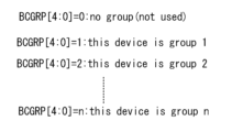
- FIG. 4 is a diagram showing an example of the correspondence between the value of the group setting data and the group to be set.
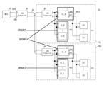
- FIG. 5 is a diagram showing an example of grouping of semiconductor devices.
- FIG. 6 is a diagram showing the data structure of receive data RX when writing is performed with the semiconductor device as the target device.
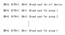
- FIG. 7 is a diagram showing an example of the correspondence between the value of a device address and the group designation for performing broadcasting.
- FIG. 1 is a diagram illustrating a configuration of a communication system according to an exemplary embodiment of the present disclosure.
- FIG. 2 is a block diagram of a semiconductor device according to an exemplary embodiment of the present disclosure.
- FIG. 3 is
- FIG. 8 is a flow diagram showing an example of each step for performing a broadcast.
- FIG. 9 is a diagram showing the data structure of received data RX when a device is accessed using the bridge function.
- FIG. 10 is a timing chart showing communication control when performing a write to a device.
- FIG. 11 is a timing chart showing communication control when performing a read from a device.
- Communication System 1 is a diagram showing a configuration of a communication system 70 according to an exemplary embodiment of the present disclosure.
- the communication system 70 includes an MCU (Micro Controller Unit) 20, a CAN (Controller Area Network) transceiver 30, a CAN transceiver 40, a semiconductor device 1, N devices 10 (N is an integer equal to or greater than 1), a plurality of semiconductor devices 50, and a plurality of semiconductor devices 60.
- the communication system 70 is, as an example, for use in a vehicle.
- the CAN transceiver 40, the semiconductor device 1, the device 10, and the semiconductor device 50 are mounted on the first board PB1.
- the CAN transceiver 40, the semiconductor device 1, the device 10, and the semiconductor device 60 are mounted on the second board PB2.
- UART Universal Asynchronous Receiver/Transmitter
- CAN is a serial communication protocol standardized in international standards such as ISO 11898.
- the CAN transceiver 30 has a TXD (transmit data input) terminal 30A and a RXD (receive data output) terminal 30B.
- the CAN transceiver 30 outputs data input to the TXD terminal 30A to the CAN bus 35, and outputs data input from the CAN bus 35 from the RXD terminal 30B.
- the CAN transceiver 40 and the semiconductor devices 1 and 50 are connected by a bus BS1.
- the bus BS1 is used for communication by UART.
- the CAN transceiver 40 has an RXD terminal 40A and a TXD terminal 40B.
- the CAN transceiver 40 outputs data input to the TXD terminal 40B to the CAN bus 35, and outputs data input from the CAN bus 35 from the RXD terminal 40A.
- the semiconductor device 1 is an IC (integrated circuit) in which circuits with specific functions are integrated, and is configured as, for example, an LED (light emitting diode) driver IC.
- the semiconductor device 1 has an RX (received data input) terminal 1A and a TX (transmitted data output) terminal 1B.
- the multiple semiconductor devices 50 are ICs in which circuits with the same or different functions as the semiconductor device 1 are integrated.
- the semiconductor device 50 has an RX terminal 50A and a TX terminal 50B, just like the semiconductor device 1.
- RX terminals 1A and 50A are commonly connected to RXD terminal 40A.
- TX terminals 1B and 50B are commonly connected to TXD terminal 40B.
- Receive data RX and transmit data TX can be communicated via bus BS1.
- Receive data RX and transmit data TX are serial data conforming to UART.
- Receive data RX output from RXD terminal 40A is input to RX terminals 1A and 50A.
- Transmit data TX output from TX terminals 1B and 50B is input to TXD terminal 40B.
- the N devices 10 are ICs in which circuits with specific functions are integrated, and are configured as, for example, matrix switch ICs.
- the semiconductor device 1 has an RXD terminal 1C and a TXD terminal 1D.
- the RX terminal 10A of each of the N devices 10 is commonly connected to the RXD terminal 1C.
- the TX terminal 10B of each of the N devices 10 is commonly connected to the TXD terminal 1D. That is, the RXD terminal 1C and the TXD terminal 1D are connected to the RX terminal 10A and the TX terminal 10B by a bus (local bus) BS2.
- Communication of received data BRX and transmitted data BTX is possible via the bus BS2.
- the received data BRX and transmitted data BTX are serial data.
- Such a bus BS2 is provided for the bridge function described below.
- the bridge function makes it possible to handle cases where the protocols of the semiconductor device 1 and the device 10 are different.
- CAN transceiver 40, semiconductor device 1, device 10, and semiconductor device 60 on the second board PB2 have the same configuration as those on the first board PB1, so detailed description will be omitted.
- Broadcasting in the communication system 70 according to this embodiment will be described below. Broadcasting is performed between the CAN transceiver 40 and the semiconductor devices 1, 5, and 60 by UART communication.
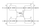
- FIG. 2 is a block diagram of a semiconductor device 1 according to an embodiment of the present disclosure.
- the semiconductor device 1 includes, as functional blocks, a first receiving unit 11, a first transmitting unit 12, a second receiving unit 13, a second transmitting unit 14, and a control unit 15.
- FIG. 2 illustrates only the functional blocks related to the communication function in the communication system 70, and other functional blocks may be included.
- the semiconductor device 1 is an LED driver, it includes a block function related to driving an LED.
- the first receiver 11 receives reception data RX via RX terminal 1A.
- the first transmitter 12 outputs reception data BRX via RXD terminal 1C.
- the second receiver 13 receives transmission data BTX via TXD terminal 1D.
- the second transmitter 14 outputs transmission data TX via TX terminal 1B.
- the control unit 15 controls the first receiving unit 11, the first transmitting unit 12, the second receiving unit 13, and the second transmitting unit 14.
- the control unit 15 has a register 151.
- the semiconductor devices 50 and 60 have the same configuration as that shown in FIG. 2 except for the first transmitting unit 12 and the second receiving unit 13.
- the register map is the correspondence between addresses in a register and stored data.
- semiconductor devices with the same register map are considered to be the same type of semiconductor device, and multiple semiconductor devices 1, 50, and 60 are provided for different types of semiconductor devices 1, 50, and 60.
- FIG. 3 is a register map relating to the grouping function in register 151 of semiconductor device 1.
- register 151 is capable of storing 8 bits of data per address
- group setting data BCGRP is stored at a specific address.
- the group setting data BCGRP is 5-bit data, and is data for setting the group of itself (semiconductor device 1) at the time of broadcasting.
- the group setting data BCGRP is stored in the lowest 5 bits of the 8 bits.
- Semiconductor devices 50 and 60 also have a register map similar to that of FIG. 3, but the specific address is not necessarily the same as that of semiconductor device 1.
- the semiconductor devices 1 are set to group 1 as shown in FIG. 5. In this way, the same type of semiconductor devices 1 mounted on different boards PB1 and PB2 can be set to the same group.
- the multiple semiconductor devices 50 are set to group 2 as shown in FIG. 5.
- the group setting can be made variable by rewriting the group setting data BCGRP via UART communication.
- the group setting is not limited to being variable, and may be fixed. In this case, the groups may be set by, for example, a resistor externally attached to the semiconductor device.
- FIG. 6 shows the data structure of the received data RX when writing to the semiconductor devices 1, 50, and 60 as the target devices.
- a frame FR is made up of bit data from a start bit S to a stop bit P.
- the start bit S is at low level, and the stop bit P is at high level.
- a predetermined number of bits of bit data are placed between the start bit S and the stop bit P.
- 8 bits of bit data are placed.
- a frame FR is made up of 10 bits of bit data.
- the received data RX includes, from the beginning, a synchronization frame SYNC, a read/write etc. frame RWD, a data count frame ND, a register address frame AD, a data frame DT, and a CRC (Cyclic Redundancy Check) frame CR.
- a synchronization frame SYNC a read/write etc. frame RWD
- a data count frame ND a data count frame ND
- a register address frame AD a data frame DT
- CRC Cyclic Redundancy Check
- the synchronization frame SYNC is bit data for setting the baud rate in the semiconductor device.
- the Read/Write etc. frame RWD includes a device address DA, a bridge bit BR, a broadcast/parity bit B/PA, and a Read/Write bit RW.
- the device address DA is bit data indicating the address of the target device (semiconductor device) (5-bit data in the example of Figure 6).
- the bridge bit BR is bit data indicating the on/off state of the bridge function of the semiconductor device 1.
- the broadcast/parity bit B/PA is bit data indicating the on/off state of the broadcast of the semiconductor device 1 or the parity of the data address DA.
- the read/write bit RW is bit data indicating Read or Write.
- broadcast/parity bit B/PA indicates whether broadcast is on or off.
- broadcast/parity bit B/PA 1, it indicates that broadcast is on.
- the broadcast/parity bit B/PA becomes the parity of the device address DA. This makes it possible to detect errors in the device address DA.
- the protocols differ for each group of devices 10 connected to each of the multiple semiconductor devices 1, turning on the broadcast of the semiconductor device 1 will result in the same receive data RX being sent as receive data BRX to devices 10 with different protocols, resulting in protocol incompatibility in some devices 10. For this reason, when the bridge function is turned on, broadcasting is not performed.
- the data number frame ND is bit data indicating the number of frames in the data frame DT.
- the register address frame AD is bit data indicating an address in a register (151, etc.).
- the data frame DT is bit data for writing to a register. Note that the data frame DT is not included in the received data RX when reading.
- the CRC frame CR is bit data indicating an error detection code added to the data frame DT.
- the CAN transceiver 40 transmits the received data RX to the semiconductor devices 1, 50, and 60.
- the control unit (control unit 15, etc.) in the semiconductor device 1, 50, and 60 judges whether the group represented by the device address DA matches the group set in its own semiconductor device. If they match, it is determined that its own semiconductor device is the target of the broadcast, and it is judged whether it is a write or a read based on the Read/Write bit RW included in the received data RX. If it is a write, writing is performed to the register based on the data frame DT included in the received data RX. If it is a read, reading is performed from the register.
- the semiconductor devices can be grouped and broadcast can be performed.
- the semiconductor device 1 and the N devices 10 support different protocols.
- the receive data RX output from the RXD terminal 40A to the RX terminal 1A includes data corresponding to the protocol of the device 10.
- the semiconductor device 1 turns on a bridge function and through-outputs the data included in the receive data RX and corresponding to the protocol of the device 10 as receive data BRX from the RXD terminal 1C.
- Through-output means that bit data is output as is.
- the device address of the device 10 is specified in the receive data BRX.
- device 10 which is the target device (the device specified by the device address) outputs transmission data BTX from TX terminal 10B to TXD terminal 1D. Because the bridge function of semiconductor device 1 is on, the transmission data BTX is output through from TX terminal 1B as transmission data TX.
- the CAN transceiver 40 can write and read to the device 10.
- FIG. 9 is a diagram showing the data structure of the received data RX when performing a write or read operation on device 10 as the target device.
- the synchronization frame SYN and the read/write frame RWD in the received data RX shown in FIG. 9 are as described above.
- the data number frame ND indicates the number of frames for the end condition of the through output, unlike the case shown in FIG. 6. Control using the data number frame ND will be described later.
- the data number frame ND is followed by device data DDT.
- the device data DDT is data that corresponds to the protocol of the device 10, and is the target to be through-output as received data BRX.
- the device data DDT includes a device address BDA.
- the device address BDA indicates the address of the device 10, which is the target device.
- the device address BDA is placed in the device data DDT at a position that corresponds to the protocol of the device 10.
- FIG. 10 is a timing chart showing communication control when performing a write to device 10. From the top of FIG. 10, receive data RX, receive data output selection signal (RX output select), transmit data output selection signal (TX output select), receive data BRX, transmit data BTX, and transmit data TX are shown (similar to FIG. 11).
- receive data RX has the configuration shown in FIG. 9.
- the received data RX is received by the first receiving unit 11 ( Figure 2).
- the control unit 15 By receiving the start bit S1 (low level) at the beginning of the received data RX, the control unit 15 recognizes the start of reception of the received data RX. After that, the control unit 15 recognizes that the bridge function is on from the bridge bit BR included in the received data RX, and recognizes that it is Write from the Read/Write bit RW.
- the control unit 15 changes the received data output selection signal in the register 151 from low to high at the stop bit P1 of the data number frame ND (timing t1). This starts the through output of the received data RX, and the first receiving unit 11 and the first transmitting unit 12 output the received data RX as it is as received data BRX. In other words, the device data DDT ( Figure 9) is output through.
- the control unit 15 When the received data output selection signal goes to high level, the control unit 15 starts counting the number of frames of received data RX (i.e., the number of frames of device data DDT). When the counted number of frames reaches the number of frames indicated by the received data number frames ND, the control unit 15 switches the received data output selection signal to low level and stops the through output (timing t2). After that, the received data BRX is fixed at high level.
- FIG. 11 is a timing chart showing communication control when performing a read on device 10.
- the received data RX has the structure shown in FIG. 9.
- the control unit 15 After receiving the start bit S1 (low level) at the beginning of the received data RX, the control unit 15 recognizes that the bridge function is on based on the bridge bit BR included in the received data RX, and recognizes that it is in a read mode based on the read/write bit RW.
- the control unit 15 changes both the received data output selection signal and the transmitted data output selection signal in the register 151 from low to high at the stop bit P1 of the data number frame ND (timing t1). This starts the through output of the received data RX and transmitted data BTX.
- the first receiving unit 11 and the first transmitting unit 12 output the received data RX as it is as received data BRX, that is, the device data DDT ( Figure 9) is through output.
- the second receiving unit 13 and the second transmitting unit 14 through output the transmitted data BTX sent from the device 10 as transmitted data TX.
- the control unit 15 When the received data output selection signal and the transmitted data output selection signal go to high level, the control unit 15 starts counting the total number of frames of the received received data RX and the received transmitted data BTX. When the counted number of frames reaches the number of frames indicated by the received data number frames ND, the control unit 15 switches both the received data output selection signal and the transmitted data output selection signal to low level, stopping the through output (timing t2). After this, the received data BRX is fixed to high level, and the transmitted data TX is fixed to Hi-z (high impedance).
- the semiconductor device (1) is A semiconductor device comprising: a receiving unit (11) configured to receive communication data (RX) from an external device through serial communication; and a control unit (15), A group of semiconductor devices can be set for the semiconductor device,
- the communication data is First data (B/PA) indicating whether or not the data is broadcast; second data (DA) representing a group of semiconductor devices;
- the control unit is configured to determine that the broadcast is directed to the semiconductor device itself if the group set in the semiconductor device itself matches the group indicated by the second data (first configuration).
- This configuration allows semiconductor devices of the same type to be grouped together for broadcasting, solving the problem of enabling effective broadcasting using serial communication.
- the second data (DA) may be configured to indicate the device address of the target semiconductor device when the first data (B/PA) indicates that the access is a normal access other than the broadcast (second configuration).
- the second data (DA) may be configured to set the communication data to be a broadcast to all semiconductor devices that receive the communication data (third configuration).
- a semiconductor device having any one of the first to third configurations can be connected to an external transmitting device (40) by a first bus (BS1) and can be connected to an external device (10) by a second bus (BS2), a first receiving unit (11) configured to be able to receive the communication data from the transmitting device via the first bus; A first transmission unit (12) configured to be connectable to the device via the second bus; Equipped with The first receiving unit and the first transmitting unit may be configured to, when bridge selection data (BR) included in the communication data indicates that a through output is on, which outputs bit data directly between the first bus and the second bus, output data (DDT) corresponding to the protocol of the device included in the communication data to the second bus (fourth configuration).
- BR bridge selection data
- DDT output data
- the first data indicates whether or not the through output is broadcast;
- the first data may represent a parity bit (fifth configuration).
- the first data (B/PA) and the second data (DA) may be included in the same frame (RWD) of the communication data together with bit data (RW) indicating Read or Write (sixth configuration).
- a register (151) is further provided,
- the group may be set by setting data (BCGRP) stored in the register (seventh configuration).
- a communication system (70) includes a transmitting device (40) configured to transmit the communication data; Any one of the first to seventh semiconductor devices (1, 50, 60) described above, The semiconductor devices having the same register map are regarded as the same type of semiconductor device, and a plurality of the semiconductor devices are provided for each of the different types of semiconductor devices (1, 50, 60) (eighth configuration).
- the semiconductor device (1) of the same type may be arranged separately on multiple substrates (PB1, PB2) (ninth configuration).
- This disclosure can be used, for example, in vehicle-mounted communication systems.
Landscapes
- Engineering & Computer Science (AREA)
- Theoretical Computer Science (AREA)
- Physics & Mathematics (AREA)
- General Engineering & Computer Science (AREA)
- General Physics & Mathematics (AREA)
- Small-Scale Networks (AREA)
Abstract
シリアル通信による通信データ(RX)を外部から受信するように構成される受信部(11)と、制御部(15)と、を備えた半導体装置(1)であって、前記半導体装置には、半導体装置のグループを設定可能であり、前記通信データは、ブロードキャストか否かを表す第1データ(B/PA)と、半導体装置のグループを表す第2データ(DA)と、を含み、前記制御部は、自身の前記半導体装置に設定された前記グループと前記第2データが示す前記グループが一致する場合、自身の前記半導体装置に対するブロードキャストであると判定する。
Description
本開示は、半導体装置、および通信システムに関する。
シリアル通信機能を備えた半導体装置が種々のアプリケーションで利用されている。
なお、シリアル通信に関する回路技術の一例は、特許文献1に開示されている。
[概要]
ここで、シリアル通信を用いてブロードキャストを行う場合の技術について、改善の余地があった。ブロードキャストとは、シリアル通信のネットワークに接続される複数の受信装置に対して1回のデータ送信によって書き込み・読み出しを行うことである。
ここで、シリアル通信を用いてブロードキャストを行う場合の技術について、改善の余地があった。ブロードキャストとは、シリアル通信のネットワークに接続される複数の受信装置に対して1回のデータ送信によって書き込み・読み出しを行うことである。
本開示は、シリアル通信を用いてブロードキャストを効果的に行うことが可能となる半導体装置を提供することを目的とする。
例えば、本開示の一態様に係る半導体装置は、
シリアル通信による通信データを外部から受信するように構成される受信部と、制御部と、を備えた半導体装置であって、
前記半導体装置には、半導体装置のグループを設定可能であり、
前記通信データは、
ブロードキャストか否かを表す第1データと、
半導体装置のグループを表す第2データと、
を含み、
前記制御部は、自身の前記半導体装置に設定された前記グループと前記第2データが示す前記グループが一致する場合、自身の前記半導体装置に対するブロードキャストであると判定する構成としている。
シリアル通信による通信データを外部から受信するように構成される受信部と、制御部と、を備えた半導体装置であって、
前記半導体装置には、半導体装置のグループを設定可能であり、
前記通信データは、
ブロードキャストか否かを表す第1データと、
半導体装置のグループを表す第2データと、
を含み、
前記制御部は、自身の前記半導体装置に設定された前記グループと前記第2データが示す前記グループが一致する場合、自身の前記半導体装置に対するブロードキャストであると判定する構成としている。
[詳細な説明]
以下、本開示の例示的な実施形態について、図面を参照して説明する。
以下、本開示の例示的な実施形態について、図面を参照して説明する。
<1.通信システム>
図1は、本開示の例示的な実施形態に係る通信システム70の構成を示す図である。通信システム70は、MCU(Micro Controller Unit)20と、CAN(Controller Area Network)トランシーバ30と、CANトランシーバ40と、半導体装置1と、N個(Nは1以上の整数)のデバイス10と、複数の半導体装置50と、複数の半導体装置60と、を備える。通信システム70は、一例として車載用である。
図1は、本開示の例示的な実施形態に係る通信システム70の構成を示す図である。通信システム70は、MCU(Micro Controller Unit)20と、CAN(Controller Area Network)トランシーバ30と、CANトランシーバ40と、半導体装置1と、N個(Nは1以上の整数)のデバイス10と、複数の半導体装置50と、複数の半導体装置60と、を備える。通信システム70は、一例として車載用である。
CANトランシーバ40と、半導体装置1と、デバイス10と、半導体装置50は、第1基板PB1に実装される。CANトランシーバ40と、半導体装置1と、デバイス10と、半導体装置60は、第2基板PB2に実装される。
MCU20とCANトランシーバ30との間では、UART(Universal Asynchronous Receiver/Transmitter)による通信が行われる。UARTは、2つのデバイス間でシリアルデータを交換するためのプロトコルである。UARTでは、送信側と受信側の間で2本のラインにより双方向の通信が行われる。
CANトランシーバ30,40との間では、CANバス35による通信が行われる。CANは、国際標準規格のISO11898等で標準化されているシリアル通信プロトコルである。
CANトランシーバ30は、TXD(送信データ入力)端子30AとRXD(受信データ出力)端子30Bを有する。CANトランシーバ30は、TXD端子30Aに入力されたデータをCANバス35へ出力し、CANバス35から入力されたデータをRXD端子30Bから出力する。
第1基板PB1において、CANトランシーバ40と半導体装置1,50との間はバスBS1により接続される。バスBS1は、UARTによる通信に用いられる。CANトランシーバ40は、RXD端子40AとTXD端子40Bを有する。CANトランシーバ40は、TXD端子40Bに入力されたデータをCANバス35へ出力し、CANバス35から入力されたデータをRXD端子40Aから出力する。
半導体装置1は、所定機能の回路が集積化されたIC(集積回路)であり、例えばLED(発光ダイオード)ドライバICとして構成される。半導体装置1は、RX(受信データ入力)端子1AとTX(送信データ出力)端子1Bを有する。複数の半導体装置50は、半導体装置1と同じあるいは異なる機能の回路が集積化されたICである。半導体装置50は、半導体装置1と同様にRX端子50AとTX端子50Bを有する。
RX端子1A,50Aは、RXD端子40Aに共通接続される。TX端子1B,50Bは、TXD端子40Bに共通接続される。バスBS1を介して受信データRXおよび送信データTXの通信が可能である。受信データRXおよび送信データTXは、UARTに準拠したシリアルデータである。RXD端子40Aから出力される受信データRXは、RX端子1A,50Aに入力される。TX端子1B,50Bから出力される送信データTXは、TXD端子40Bに入力される。
N個のデバイス10は、所定機能の回路が集積化されたICであり、例えばマトリクススイッチICとして構成される。
半導体装置1は、RXD端子1CおよびTXD端子1Dを有する。N個のデバイス10のそれぞれのRX端子10Aは、RXD端子1Cに共通接続される。N個のデバイス10のそれぞれのTX端子10Bは、TXD端子1Dに共通接続される。すなわち、RXD端子1C,TXD端子1Dは、バス(ローカルバス)BS2によりRX端子10A,TX端子10Bに接続される。バスBS2を介して受信データBRXおよび送信データBTXの通信が可能である。受信データBRXおよび送信データBTXは、シリアルデータである。
このようなバスBS2は、後述するブリッジ機能のために設けられる。ブリッジ機能によって、半導体装置1とデバイス10のプロトコルが異なっている場合でも対応が可能となる。
なお、第2基板PB2におけるCANトランシーバ40、半導体装置1、デバイス10、および半導体装置60については、第1基板PB1における構成と同様であるため、詳述は省く。
<2.ブロードキャストについて>
本実施形態に係る通信システム70におけるブロードキャストについて、以下説明する。ブロードキャストは、CANトランシーバ40と半導体装置1,5,60との間でUART通信によって行われる。
本実施形態に係る通信システム70におけるブロードキャストについて、以下説明する。ブロードキャストは、CANトランシーバ40と半導体装置1,5,60との間でUART通信によって行われる。
図2は、本開示の実施形態に係る半導体装置1のブロック図である。半導体装置1は、機能ブロックとして、第1受信部11、第1送信部12、第2受信部13、第2送信部14、および制御部15を備える。なお、図2は、通信システム70における通信機能に関する機能ブロックのみを図示しており、その他の機能ブロックを備えてもよい。例えば、半導体装置1がLEDドライバである場合は、LED駆動に関するブロック機能を備える。
第1受信部11は、RX端子1Aを介して受信データRXを受信する。第1送信部12は、RXD端子1Cを介して受信データBRXを出力する。第2受信部13は、TXD端子1Dを介して送信データBTXを受信する。第2送信部14は、TX端子1Bを介して送信データTXを出力する。
制御部15は、第1受信部11、第1送信部12、第2受信部13、および第2送信部14を制御する。制御部15は、レジスタ151を有する。
なお、半導体装置50,60は、図2における第1送信部12および第2受信部13を除く構成と同様の構成を有する。
半導体装置1,5,60の各レジスタ(レジスタ151等)におけるレジスタマップが異なる場合、CANトランシーバ40からの1回のデータ送信で半導体装置1,5,60のすべてに対して書き込み・読み出しを行うようなブロードキャストは困難である。なお、レジスタマップは、レジスタにおけるアドレスと格納データとの対応関係である。図1の例では、同じレジスタマップの半導体装置を同一種類の半導体装置として、異なる種類の半導体装置1,50,60ごとに半導体装置1,50,60は複数設けられる。
そこで、本実施形態では、ブロードキャストを行う対象の半導体装置をグループ化するグループ化機能が備えられる。図3は、半導体装置1のレジスタ151におけるグループ化機能に関するレジスタマップである。具体的には、レジスタ151では、1つのアドレスに対して8ビットのデータが格納可能であり、図3では、所定のアドレスに対してグループ設定データBCGRPが格納される。グループ設定データBCGRPは、5ビットのデータであり、ブロードキャスト時の自身(半導体装置1)のグループを設定するためのデータである。図3では、グループ設定データBCGRPは、8ビットのうち下位5ビットに格納される。なお、半導体装置50,60も図3と同様なレジスタマップを有するが、上記所定のアドレスは半導体装置1と同じであるとは限らない。
グループ設定データBCGRPは、0~31の値をとることが可能である。図4に示すように、例えば、BCGRP=1の場合、グループ1が設定され、BCGRP=2の場合、グループ2が設定される。すなわち、BCGRP=nの場合、グループnが設定される(nは1~31のいずれかの値)。なお、BCGRP=0の場合は、グループ設定しない。
例えば、基板PB1,PB2にそれぞれ実装される半導体装置1のそれぞれにおいて、ともにBCGRP=1の場合、図5に示すように上記半導体装置1はグループ1に設定される。このように、異なる基板PB1,PB2に実装される同一種類の半導体装置1を同じグループに設定できる。
また、複数の半導体装置50において、いずれにおいてもBCGRP=2の場合、図5に示すように複数の半導体装置50はグループ2に設定される。同様に、複数の半導体装置60において、いずれにおいてもBCGRP=3の場合、図5に示すように複数の半導体装置60はグループ3に設定される。
また、レジスタに格納されるグループ設定データBCGRPによってグループ設定するため、UART通信によってグループ設定データBCGRPを書き換えることで、グループ設定を可変とすることができる。なお、グループ設定は、可変に限らず、固定としてもよい。この場合、例えば半導体装置に対して外付けされる抵抗によってグループ設定してもよい。
図6は、半導体装置1,50,60を対象デバイスとしてWriteを行う場合の受信データRXのデータ構成を示す図である。
UARTでは、フレームと呼ばれるデータ単位により通信が行われる。図6に示すように、フレームFRは、スタートビットSからストップビットPまでのビットデータで構成される。スタートビットSはローレベル、ストップビットPはハイレベルとなる。スタートビットSとストップビットPの間には、所定ビット数のビットデータが配置される。図6の例では、8ビットのビットデータが配置される。すなわち、フレームFRは、10ビットのビットデータから構成される。
図6に示すように、受信データRXは、同期フレームSYNC、Read/Write等フレームRWD、データ数フレームND、レジスタアドレスフレームAD、データフレームDT、およびCRC(Cyclic Redundancy Check)フレームCRを先頭から順に有する。
同期フレームSYNCは、半導体装置にボーレートを設定するためのビットデータである。
Read/Write等フレームRWDは、デバイスアドレスDA、ブリッジビットBR、ブロードキャスト/パリティビットB/PA、およびRead/WriteビットRWを含む。
デバイスアドレスDAは、対象デバイス(半導体装置)のアドレスを示すビットデータである(図6の例では5ビットデータ)。ブリッジビットBRは、半導体装置1のブリッジ機能のオンオフを示すビットデータである。ブロードキャスト/パリティビットB/PAは、半導体装置1のブロードキャストのオンオフあるいはデータアドレスDAのパリティを示すビットデータである。Read/WriteビットRWは、Read(読み出し)あるいはWrite(書き込み)を示すビットデータである。
ブリッジビットBR=0でブリッジ機能のオフ、すなわち通常モードを示す。この場合、ブロードキャスト/パリティビットB/PAは、ブロードキャストのオンオフを示す。ブロードキャスト/パリティビットB/PA=0の場合、ブロードキャストのオフを示し、ブロードキャスト/パリティビットB/PA=1の場合、ブロードキャストのオンを示す。
ブリッジビットBR=1でブリッジ機能のオンを示す。この場合、ブロードキャスト/パリティビットB/PAは、デバイスアドレスDAのパリティとなる。これにより、デバイスアドレスDAの誤り検出を行うことができる。なお、図1に示す構成において、複数の半導体装置1それぞれに接続されるデバイス10のグループごとにプロトコルが異なる場合、半導体装置1のブロードキャストをオンとすると、同じ受信データRXが受信データBRXとして異なるプロトコルのデバイス10に送信されることになり、一部のデバイス10ではプロトコルが不適合となってしまう。そこで、ブリッジ機能をオンとする場合は、ブロードキャストは行わないようにしている。
データ数フレームNDは、データフレームDTのフレーム数を示すビットデータである。レジスタアドレスフレームADは、レジスタ(151等)におけるアドレスを示すビットデータである。データフレームDTは、レジスタへの書き込みのためのビットデータである。なお、データフレームDTは、リード時には受信データRXに含められない。CRCフレームCRは、データフレームDTに対して付加される誤り検出符号を示すビットデータである。
BR=0かつB/PA=1、すなわちブリッジ機能がオフ、かつブロードキャストがオンの場合、デバイスアドレスDAは、グループを示すデータとして使用される。例えば、図7に示すように、DA=1がグループ1、DA=2がグループ2、すなわちDA=nがグループnを示す。従って、グループを示すデータとしてデバイスアドレスDAを流用することで、通信量が増加することを回避できる。なお、BR=0かつB/PA=0、すなわちブリッジ機能がオフ、かつブロードキャストがオフ(通常アクセス)の場合、デバイスアドレスDAは、本来のデバイスアドレスを示す。
上記のように半導体装置1,50,60にグループ設定後に、ブロードキャストを行う場合、CANトランシーバ40から半導体装置1,50,60に対して受信データRXが送信される。この場合、受信データRXにおいて、BR=0かつB/PA=1、すなわちブリッジ機能がオフ、かつブロードキャストがオンに設定されている。すると、半導体装置1,50,60における制御部(制御部15等)は、デバイスアドレスDAで表されるグループが自身の半導体装置に設定されているグループと一致するかを判定する。もし一致する場合は、自身の半導体装置がブロードキャストの対象であるとして、受信された受信データRXに含まれるRead/WriteビットRWに基づいて書き込みであるか読み出しであるかが判定される。書き込みである場合は、受信データRXに含まれるデータフレームDTに基づいてレジスタへの書き込みを行う。読み出しである場合は、レジスタからの読み出しを行う。
例えば、図8に示すフローのように、グループ設定データBCGRPによって半導体装置1,50,60がそれぞれグループ1,2,3に設定された後に、BR=0かつB/PA=1かつDA=1である受信データRXを送信すれば、半導体装置1に対するブロードキャストとなり、BR=0かつB/PA=1かつDA=2である受信データRXを送信すれば、半導体装置50に対するブロードキャストとなり、BR=0かつB/PA=1かつDA=3である受信データRXを送信すれば、半導体装置60に対するブロードキャストとなる。
このような本実施形態によれば、半導体装置1,50,60でレジスタにおけるレジスタマップが異なる場合でも、各半導体装置をグループ化して、ブロードキャストを行うことができる。
なお、図7に示すようにデバイスアドレスDA=0とすれば、半導体装置1,50,60すべてに対するブロードキャストとなる。半導体装置1,50,60のレジスタマップが同じである場合に有効である。
<3.ブリッジ機能について>
図1に示す構成においては、半導体装置1とN個のデバイス10とで対応するプロトコルが異なっている。CANトランシーバ40がデバイス10に対してWrite(書き込み)あるいはRead(読み出し)を行う場合、RXD端子40AからRX端子1Aに出力される受信データRXには、デバイス10のプロトコルに対応するデータが含まれる。このとき、半導体装置1は、ブリッジ機能をオンとして、受信データRXに含まれるデバイス10のプロトコルに対応するデータを受信データBRXとしてRXD端子1Cからスルー出力する。スルー出力とは、ビットデータをそのまま出力することである。受信データBRXには、デバイス10のデバイスアドレスが指定される。
図1に示す構成においては、半導体装置1とN個のデバイス10とで対応するプロトコルが異なっている。CANトランシーバ40がデバイス10に対してWrite(書き込み)あるいはRead(読み出し)を行う場合、RXD端子40AからRX端子1Aに出力される受信データRXには、デバイス10のプロトコルに対応するデータが含まれる。このとき、半導体装置1は、ブリッジ機能をオンとして、受信データRXに含まれるデバイス10のプロトコルに対応するデータを受信データBRXとしてRXD端子1Cからスルー出力する。スルー出力とは、ビットデータをそのまま出力することである。受信データBRXには、デバイス10のデバイスアドレスが指定される。
Readの場合、対象デバイス(デバイスアドレスで指定されるデバイス)であるデバイス10は、TX端子10BからTXD端子1Dに送信データBTXを出力する。半導体装置1は、ブリッジ機能がオンのため、送信データBTXを送信データTXとしてTX端子1Bからスルー出力する。
このように本開示の実施形態によれば、半導体装置1とデバイス10のプロトコルが異なっている場合でも、CANトランシーバ40は、デバイス10に対してWriteおよびReadを行うことができる。
図9は、デバイス10を対象デバイスとしてWriteあるいはReadを行う場合の受信データRXのデータ構成を示す図である。図9に示す受信データRXにおける同期フレームSYNおよびRead/Write等フレームRWDは、先述の通りである。
図9に示す受信データRXにおいて、データ数フレームNDは、図6に示す場合と異なり、スルー出力の終了条件のためのフレーム数を示す。データ数フレームNDを用いた制御については、後述する。
図9に示す受信データRXにおいては、データ数フレームNDの後にデバイスデータDDTが続く。デバイスデータDDTは、デバイス10のプロトコルに対応するデータであり、受信データBRXとしてスルー出力される対象である。デバイスデータDDTは、デバイスアドレスBDAを含む。デバイスアドレスBDAは、対象デバイスであるデバイス10のアドレスを示す。デバイスアドレスBDAがデバイスデータDDTにおいて配置される位置は、デバイス10のプロトコルに応じた位置となる。
ここで、半導体装置1によるスルー出力制御、すなわちブリッジ機能がオンの場合の制御について述べる。
図10は、デバイス10に対するWriteを行う場合の通信制御を示すタイミングチャートである。図10の上段から順に、受信データRX、受信データ出力選択信号(RX output select)、送信データ出力選択信号(TX output select)、受信データBRX、送信データBTX、および送信データTXを示す(図11でも同様)。受信データRXは、図9に示す構成となる。
受信データRXは、第1受信部11(図2)により受信される。受信データRXの先頭のスタートビットS1(ローレベル)を受信したことにより、制御部15は、受信データRXの受信開始を認識する。その後、制御部15は、受信データRXに含まれるブリッジビットBRによりブリッジ機能がオンであることを認識するとともに、Read/WriteビットRWによりWriteであることを認識する。
その後、データ数フレームNDが受信されると、データ数フレームNDのストップビットP1で制御部15は、レジスタ151における受信データ出力選択信号をローレベルからハイレベルとする(タイミングt1)。これにより、受信データRXのスルー出力が開始され、第1受信部11および第1送信部12は、受信データRXをそのまま受信データBRXとして出力する。すなわち、デバイスデータDDT(図9)のスルー出力が行われる。
受信データ出力選択信号がハイレベルになったときに制御部15は、受信される受信データRXのフレーム数(すなわち、デバイスデータDDTのフレーム数)のカウントを開始する。カウントしたフレーム数が受信されたデータ数フレームNDが示すフレーム数に到達すると、制御部15は、受信データ出力選択信号をローレベルに切り替え、スルー出力を停止させる(タイミングt2)。以降、受信データBRXは、ハイレベル固定となる。
図11は、デバイス10に対するReadを行う場合の通信制御を示すタイミングチャートである。この場合、受信データRXは、図9に示す構成となる。
受信データRXの先頭のスタートビットS1(ローレベル)が受信された後、制御部15は、受信データRXに含まれるブリッジビットBRによりブリッジ機能がオンであることを認識するとともに、Read/WriteビットRWによりReadであることを認識する。
その後、データ数フレームNDが受信されると、データ数フレームNDのストップビットP1で制御部15は、レジスタ151における受信データ出力選択信号および送信データ出力選択信号をともにローレベルからハイレベルとする(タイミングt1)。これにより、受信データRXおよび送信データBTXのスルー出力が開始される。第1受信部11および第1送信部12は、受信データRXをそのまま受信データBRXとして出力し、すなわち、デバイスデータDDT(図9)のスルー出力が行われる。受信データBRXの出力完了後、第2受信部13および第2送信部14は、デバイス10から送られる送信データBTXを送信データTXとしてスルー出力する。
受信データ出力選択信号および送信データ出力選択信号がハイレベルになったときに制御部15は、受信される受信データRXと受信される送信データBTXのフレーム数の総和のカウントを開始する。カウントしたフレーム数が受信されたデータ数フレームNDが示すフレーム数に到達すると、制御部15は、受信データ出力選択信号および送信データ出力選択信号をともにローレベルに切り替え、スルー出力を停止させる(タイミングt2)。以降、受信データBRXは、ハイレベル固定となり、送信データTXはHi-z(ハイインピーダンス)固定となる。
<4.その他>
なお、本明細書中に開示されている種々の技術的特徴は、上記実施形態のほか、その技術的創作の主旨を逸脱しない範囲で種々の変更を加えることが可能である。すなわち、上記実施形態は、全ての点で例示であって制限的なものではないと考えられるべきであり、本開示の技術的範囲は、上記実施形態に限定されるものではなく、特許請求の範囲と均等の意味および範囲内に属する全ての変更が含まれると理解されるべきである。
なお、本明細書中に開示されている種々の技術的特徴は、上記実施形態のほか、その技術的創作の主旨を逸脱しない範囲で種々の変更を加えることが可能である。すなわち、上記実施形態は、全ての点で例示であって制限的なものではないと考えられるべきであり、本開示の技術的範囲は、上記実施形態に限定されるものではなく、特許請求の範囲と均等の意味および範囲内に属する全ての変更が含まれると理解されるべきである。
<5.付記>
以上のように、本開示の一態様に係る半導体装置(1)は、
シリアル通信による通信データ(RX)を外部から受信するように構成される受信部(11)と、制御部(15)と、を備えた半導体装置であって、
前記半導体装置には、半導体装置のグループを設定可能であり、
前記通信データは、
ブロードキャストか否かを表す第1データ(B/PA)と、
半導体装置のグループを表す第2データ(DA)と、
を含み、
前記制御部は、自身の前記半導体装置に設定された前記グループと前記第2データが示す前記グループが一致する場合、自身の前記半導体装置に対するブロードキャストであると判定する構成としている(第1の構成)。
以上のように、本開示の一態様に係る半導体装置(1)は、
シリアル通信による通信データ(RX)を外部から受信するように構成される受信部(11)と、制御部(15)と、を備えた半導体装置であって、
前記半導体装置には、半導体装置のグループを設定可能であり、
前記通信データは、
ブロードキャストか否かを表す第1データ(B/PA)と、
半導体装置のグループを表す第2データ(DA)と、
を含み、
前記制御部は、自身の前記半導体装置に設定された前記グループと前記第2データが示す前記グループが一致する場合、自身の前記半導体装置に対するブロードキャストであると判定する構成としている(第1の構成)。
このような構成によれば、同じ種類の半導体装置をグループ化してブロードキャストを行うことができるため、シリアル通信を用いてブロードキャストを効果的に行うことを可能とする課題を解決できる。
また、上記第1の構成において、前記第2データ(DA)は、前記第1データ(B/PA)が前記ブロードキャストではない通常のアクセスであることを示す場合、対象とする半導体装置のデバイスアドレスを示す構成としてもよい(第2の構成)。
また、上記第1または第2の構成において、前記第1データ(B/PA)が前記ブロードキャストを示す場合、前記第2データ(DA)により、前記通信データが受信されるすべての半導体装置に対するブロードキャストであることを設定可能である構成としてもよい(第3の構成)。
また、外部の送信装置(40)と第1バス(BS1)により接続可能、かつ外部のデバイス(10)と第2バス(BS2)により接続可能な上記第1から第3のいずれかの構成の半導体装置であって、
前記送信装置から前記第1バスを介して前記通信データを受信可能に構成される第1受信部(11)と、
前記デバイスと前記第2バスを介して接続可能に構成される第1送信部(12)と、
を備え、
前記第1受信部および前記第1送信部は、前記通信データに含まれるブリッジ選択データ(BR)が前記第1バスと前記第2バスとの間でビットデータをそのまま出力するスルー出力のオンを示している場合、前記通信データに含まれる前記デバイスのプロトコルに対応したデータ(DDT)を前記第2バスへスルー出力するように構成されることとしてもよい(第4の構成)。
前記送信装置から前記第1バスを介して前記通信データを受信可能に構成される第1受信部(11)と、
前記デバイスと前記第2バスを介して接続可能に構成される第1送信部(12)と、
を備え、
前記第1受信部および前記第1送信部は、前記通信データに含まれるブリッジ選択データ(BR)が前記第1バスと前記第2バスとの間でビットデータをそのまま出力するスルー出力のオンを示している場合、前記通信データに含まれる前記デバイスのプロトコルに対応したデータ(DDT)を前記第2バスへスルー出力するように構成されることとしてもよい(第4の構成)。
また、上記第4の構成において、前記ブリッジ選択データ(BR)が前記スルー出力のオフを示す場合、前記第1データ(B/PA)は、前記ブロードキャストか否かを表し、
前記ブリッジ選択データが前記スルー出力のオンを示す場合、前記第1データは、パリティビットを表す構成としてもよい(第5の構成)。
前記ブリッジ選択データが前記スルー出力のオンを示す場合、前記第1データは、パリティビットを表す構成としてもよい(第5の構成)。
また、上記第1から第5のいずれかの構成において、前記第1データ(B/PA)および前記第2データ(DA)は、ReadあるいはWriteを示すビットデータ(RW)とともに前記通信データにおける同一フレーム(RWD)に含まれる構成としてもよい(第6の構成)。
また、上記第1から第6のいずれかの構成において、レジスタ(151)をさらに備え、
前記グループは、前記レジスタに格納される設定データ(BCGRP)により設定可能である構成としてもよい(第7の構成)。
前記グループは、前記レジスタに格納される設定データ(BCGRP)により設定可能である構成としてもよい(第7の構成)。
また、本開示の一態様に係る通信システム(70)は、前記通信データを送信するように構成される送信装置(40)と、
上記第1から第7のいずれかの半導体装置(1,50,60)と、を備え、
同じレジスタマップの前記半導体装置を同一種類の前記半導体装置として、異なる種類の前記半導体装置(1,50,60)ごとに前記半導体装置が複数設けられる構成としている(第8の構成)。
上記第1から第7のいずれかの半導体装置(1,50,60)と、を備え、
同じレジスタマップの前記半導体装置を同一種類の前記半導体装置として、異なる種類の前記半導体装置(1,50,60)ごとに前記半導体装置が複数設けられる構成としている(第8の構成)。
また、上記第8の構成において、前記同一種類の前記半導体装置(1)が複数の基板(PB1,PB2)に分けて配置される構成としてもよい(第9の構成)。
本開示は、例えば、車載用の通信システムに利用することが可能である。
1 半導体装置
1A RX端子
1B TX端子
1C RXD端子
1D TXD端子
10 デバイス
10A RX端子
10B TX端子
11 第1受信部
12 第1送信部
13 第2受信部
14 第2送信部
15 制御部
30 CANトランシーバ
30A TXD端子
30B RXD端子
35 CANバス
40 CANトランシーバ
40A RXD端子
40B TXD端子
50 半導体装置
60 半導体装置
70 通信システム
151 レジスタ
BS1,BS2 バス
PB1 第1基板
PB2 第2基板
1A RX端子
1B TX端子
1C RXD端子
1D TXD端子
10 デバイス
10A RX端子
10B TX端子
11 第1受信部
12 第1送信部
13 第2受信部
14 第2送信部
15 制御部
30 CANトランシーバ
30A TXD端子
30B RXD端子
35 CANバス
40 CANトランシーバ
40A RXD端子
40B TXD端子
50 半導体装置
60 半導体装置
70 通信システム
151 レジスタ
BS1,BS2 バス
PB1 第1基板
PB2 第2基板
Claims (9)
- シリアル通信による通信データを外部から受信するように構成される受信部と、制御部と、を備えた半導体装置であって、
前記半導体装置には、半導体装置のグループを設定可能であり、
前記通信データは、
ブロードキャストか否かを表す第1データと、
半導体装置のグループを表す第2データと、
を含み、
前記制御部は、自身の前記半導体装置に設定された前記グループと前記第2データが示す前記グループが一致する場合、自身の前記半導体装置に対するブロードキャストであると判定する、半導体装置。 - 前記第2データは、前記第1データが前記ブロードキャストではない通常のアクセスであることを示す場合、対象とする半導体装置のデバイスアドレスを示す、請求項1に記載の半導体装置。
- 前記第1データが前記ブロードキャストを示す場合、前記第2データにより、前記通信データが受信されるすべての半導体装置に対するブロードキャストであることを設定可能である、請求項1または請求項2に記載の半導体装置。
- 外部の送信装置と第1バスにより接続可能、かつ外部のデバイスと第2バスにより接続可能な請求項1から請求項3のいずれか1項に記載の半導体装置であって、
前記送信装置から前記第1バスを介して前記通信データを受信可能に構成される第1受信部と、
前記デバイスと前記第2バスを介して接続可能に構成される第1送信部と、
を備え、
前記第1受信部および前記第1送信部は、前記通信データに含まれるブリッジ選択データが前記第1バスと前記第2バスとの間でビットデータをそのまま出力するスルー出力のオンを示している場合、前記通信データに含まれる前記デバイスのプロトコルに対応したデータを前記第2バスへスルー出力するように構成される、半導体装置。 - 前記ブリッジ選択データが前記スルー出力のオフを示す場合、前記第1データは、前記ブロードキャストか否かを表し、
前記ブリッジ選択データが前記スルー出力のオンを示す場合、前記第1データは、パリティビットを表す、請求項4に記載の半導体装置。 - 前記第1データおよび前記第2データは、ReadあるいはWriteを示すビットデータとともに前記通信データにおける同一フレームに含まれる、請求項1から請求項5のいずれか1項に記載の半導体装置。
- レジスタをさらに備え、
前記グループは、前記レジスタに格納される設定データにより設定可能である、請求項1から請求項6のいずれか1項に記載の半導体装置。 - 前記通信データを送信するように構成される送信装置と、
請求項1から請求項7のいずれか1項に記載の半導体装置と、を備え、
同じレジスタマップの前記半導体装置を同一種類の前記半導体装置として、異なる種類の前記半導体装置ごとに前記半導体装置が複数設けられる、通信システム。 - 前記同一種類の前記半導体装置が複数の基板に分けて配置される、請求項8に記載の通信システム。
Priority Applications (2)
| Application Number | Priority Date | Filing Date | Title |
|---|---|---|---|
| CN202480044371.1A CN121444081A (zh) | 2023-07-06 | 2024-06-12 | 半导体装置以及通信系统 |
| JP2025531454A JPWO2025009346A1 (ja) | 2023-07-06 | 2024-06-12 |
Applications Claiming Priority (2)
| Application Number | Priority Date | Filing Date | Title |
|---|---|---|---|
| JP2023111351 | 2023-07-06 | ||
| JP2023-111351 | 2023-07-06 |
Related Child Applications (1)
| Application Number | Title | Priority Date | Filing Date |
|---|---|---|---|
| US19/436,540 Continuation US20260128758A1 (en) | 2023-07-06 | 2025-12-30 | Semiconductor device and communication system |
Publications (1)
| Publication Number | Publication Date |
|---|---|
| WO2025009346A1 true WO2025009346A1 (ja) | 2025-01-09 |
Family
ID=94171651
Family Applications (1)
| Application Number | Title | Priority Date | Filing Date |
|---|---|---|---|
| PCT/JP2024/021377 Ceased WO2025009346A1 (ja) | 2023-07-06 | 2024-06-12 | 半導体装置、および通信システム |
Country Status (3)
| Country | Link |
|---|---|
| JP (1) | JPWO2025009346A1 (ja) |
| CN (1) | CN121444081A (ja) |
| WO (1) | WO2025009346A1 (ja) |
Citations (2)
| Publication number | Priority date | Publication date | Assignee | Title |
|---|---|---|---|---|
| JP2000286872A (ja) * | 1999-03-30 | 2000-10-13 | Kawasaki Steel Corp | シリアルデータ転送装置 |
| JP2001067107A (ja) * | 1999-08-30 | 2001-03-16 | Mitsubishi Electric Corp | プログラマブルコントローラシステムおよびその情報伝送制御方法 |
-
2024
- 2024-06-12 JP JP2025531454A patent/JPWO2025009346A1/ja active Pending
- 2024-06-12 CN CN202480044371.1A patent/CN121444081A/zh active Pending
- 2024-06-12 WO PCT/JP2024/021377 patent/WO2025009346A1/ja not_active Ceased
Patent Citations (2)
| Publication number | Priority date | Publication date | Assignee | Title |
|---|---|---|---|---|
| JP2000286872A (ja) * | 1999-03-30 | 2000-10-13 | Kawasaki Steel Corp | シリアルデータ転送装置 |
| JP2001067107A (ja) * | 1999-08-30 | 2001-03-16 | Mitsubishi Electric Corp | プログラマブルコントローラシステムおよびその情報伝送制御方法 |
Also Published As
| Publication number | Publication date |
|---|---|
| JPWO2025009346A1 (ja) | 2025-01-09 |
| CN121444081A (zh) | 2026-01-30 |
Similar Documents
| Publication | Publication Date | Title |
|---|---|---|
| US12120010B2 (en) | Error detection test device for a subscriber station of a serial bus system and method for testing mechanisms for detecting errors in a communication in a serial bus system | |
| US11106618B2 (en) | Method for addressing an integrated circuit on a bus and corresponding device | |
| US10523462B2 (en) | Communication network for transmission of messages | |
| CN100462955C (zh) | 用来与sata装置进行通讯的代用sata主控装置及其相关方法 | |
| US8307137B2 (en) | Remote communication method of a network | |
| JP3757204B2 (ja) | エラー検出/訂正方式及び該方式を用いた制御装置 | |
| US20050144339A1 (en) | Speculative processing of transaction layer packets | |
| CN101304362A (zh) | 重传缓冲装置及传输数据的方法 | |
| WO2025009346A1 (ja) | 半導体装置、および通信システム | |
| WO2002021775A1 (en) | Plural station memory data sharing system | |
| US20260128758A1 (en) | Semiconductor device and communication system | |
| CN118381721B (zh) | 一种在a-phy系统中用i2c广播配置串行器或传感器的方法 | |
| US7065621B2 (en) | System and method for implementing a hidden address in a communication module | |
| US6732207B2 (en) | Fast serial interface used for controller to robot communications | |
| WO2024009733A1 (ja) | 半導体装置、および通信システム | |
| US11863468B2 (en) | Control of ethernet link-partner GPIO using OAM | |
| EP0569512A4 (en) | Packet transmission system and method utilizing both a data bus and dedicated control lines | |
| JP4970563B2 (ja) | 複数の非ファイバ・チャネル装置をファイバ・チャネル調停ループに結合させるブリッジ装置および方法 | |
| US20260127133A1 (en) | Semiconductor device and communication system | |
| CN101189593A (zh) | 在多路复用的地址/数据总线上进行地址传输期间传送冗余数据的方法 | |
| WO2025009266A1 (ja) | 半導体装置、および通信システム | |
| KR100612454B1 (ko) | I2c 버스 정합 장치 및 방법 | |
| US6460092B1 (en) | Integrated circuit for distributed-type input/output control | |
| US20080091788A1 (en) | Controller, address control method, and data transmission system using the same | |
| US6944176B1 (en) | Method and apparatus for bit level network data multiplexing |
Legal Events
| Date | Code | Title | Description |
|---|---|---|---|
| 121 | Ep: the epo has been informed by wipo that ep was designated in this application |
Ref document number: 24835863 Country of ref document: EP Kind code of ref document: A1 |
|
| ENP | Entry into the national phase |
Ref document number: 2025531454 Country of ref document: JP Kind code of ref document: A |
|
| WWE | Wipo information: entry into national phase |
Ref document number: 2025531454 Country of ref document: JP |
|
| NENP | Non-entry into the national phase |
Ref country code: DE |