WO2025009337A1 - 光導波路基板、光学モジュール、および光導波路基板の製造方法 - Google Patents
光導波路基板、光学モジュール、および光導波路基板の製造方法 Download PDFInfo
- Publication number
- WO2025009337A1 WO2025009337A1 PCT/JP2024/021063 JP2024021063W WO2025009337A1 WO 2025009337 A1 WO2025009337 A1 WO 2025009337A1 JP 2024021063 W JP2024021063 W JP 2024021063W WO 2025009337 A1 WO2025009337 A1 WO 2025009337A1
- Authority
- WO
- WIPO (PCT)
- Prior art keywords
- optical waveguide
- markers
- marker
- glass substrate
- optical
- Prior art date
- Legal status (The legal status is an assumption and is not a legal conclusion. Google has not performed a legal analysis and makes no representation as to the accuracy of the status listed.)
- Ceased
Links
Images


Classifications
-
- G—PHYSICS
- G02—OPTICS
- G02B—OPTICAL ELEMENTS, SYSTEMS OR APPARATUS
- G02B6/00—Light guides; Structural details of arrangements comprising light guides and other optical elements, e.g. couplings
- G02B6/10—Light guides; Structural details of arrangements comprising light guides and other optical elements, e.g. couplings of the optical waveguide type
- G02B6/12—Light guides; Structural details of arrangements comprising light guides and other optical elements, e.g. couplings of the optical waveguide type of the integrated circuit kind
- G02B6/122—Basic optical elements, e.g. light-guiding paths
-
- G—PHYSICS
- G02—OPTICS
- G02B—OPTICAL ELEMENTS, SYSTEMS OR APPARATUS
- G02B6/00—Light guides; Structural details of arrangements comprising light guides and other optical elements, e.g. couplings
- G02B6/24—Coupling light guides
- G02B6/26—Optical coupling means
- G02B6/30—Optical coupling means for use between fibre and thin-film device
Definitions
- This disclosure relates to an optical waveguide substrate, an optical module, and a method for manufacturing an optical waveguide substrate.
- This application claims priority to Japanese Application No. 2023-110707, filed on July 5, 2023, and incorporates all of the contents of said Japanese application by reference.
- Patent Document 1 discloses a method for forming an optical waveguide in a transparent crystal substrate having linear and nonlinear optical properties. This method includes the steps of irradiating a first substrate having linear optical properties with a femtosecond laser to form a first optical waveguide, aligning the position for bonding the first substrate on which the first optical waveguide is formed to a second substrate having nonlinear optical properties, and bonding the aligned first substrate and second substrate to form a transparent crystal substrate.
- An optical waveguide substrate includes a glass substrate.
- the glass substrate has an optical waveguide section including one or more optical waveguides formed inside the glass substrate, and a plurality of markers that are provided inside the glass substrate and serve as indicators for the positions of the one or more optical waveguides.
- the plurality of markers are provided at fixed relative positions in the thickness direction of the glass substrate with respect to the closest portion of the optical waveguide section, and are spaced apart from the optical waveguide section when viewed along the thickness direction.
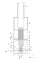
- FIG. 1 is a perspective view illustrating an optical module according to an embodiment of the present disclosure.
- FIG. 2 is a plan view illustrating an optical module according to an embodiment of the present disclosure.
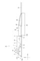
- FIG. 3 is a side view illustrating an optical module according to an embodiment of the present disclosure.
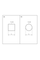
- FIG. 4 is a schematic diagram showing a cross section perpendicular to the extending direction of the optical waveguide.
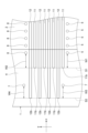
- FIG. 5 is an enlarged plan view showing the glass substrate.
- FIG. 6 is a partial cross-sectional view taken along the line VI-VI shown in FIG.
- FIG. 7 is a schematic diagram showing a cross section of a marker.
- FIG. 8 is a flowchart showing a method for manufacturing an optical module.
- An optical waveguide may be formed inside a glass substrate.
- the difference in refractive index between the glass substrate and the optical waveguide is small, it is difficult to visually recognize the optical waveguide. Therefore, the position of the optical waveguide cannot be efficiently identified, and there is a problem that it takes time to align the optical waveguide and the optical component connected to the optical waveguide.
- An optical waveguide substrate includes a glass substrate.
- the glass substrate has an optical waveguide section including one or more optical waveguides formed inside the glass substrate, and a plurality of markers that are provided inside the glass substrate and serve as indicators for the positions of the one or more optical waveguides.
- the plurality of markers are provided at fixed relative positions in the thickness direction of the glass substrate with respect to the closest portion of the optical waveguide section, and are spaced apart from the optical waveguide section when viewed along the thickness direction.
- a number of markers are provided inside the glass substrate as indicators of the position of the optical waveguide.
- the relative positional relationship between the number of markers and the optical waveguide is predetermined, so by visually checking the number of markers, the position of the optical waveguide formed inside the glass substrate can be easily identified.
- the number of markers are provided at fixed relative positions in the thickness direction of the glass substrate to the closest part of the optical waveguide portion, making it easy to evaluate the relative positional relationship between the number of markers and the optical waveguide.
- the number of markers are separated from the optical waveguide portion when viewed along the thickness direction of the glass substrate, so that the number of markers can be easily visually checked from the thickness direction of the glass substrate.
- the multiple markers may be provided in an area close to one plate surface facing the thickness direction of the glass substrate relative to the closest portion of the optical waveguide.
- the intensity of the laser light when forming the multiple markers is made greater than the intensity of the laser light when forming the optical waveguide in order to increase the visibility of the multiple markers.
- the multiple markers are formed using the same optical system as that used to form the optical waveguide, the multiple markers are formed in an area close to the laser light incidence surface relative to the optical waveguide due to the difference in the intensity of the laser light.
- the optical waveguide and the multiple markers can be formed without changing the optical system. This simplifies the process of forming the optical waveguide and the multiple markers.
- the positions of the multiple markers in the thickness direction of the glass substrate may be the same as the positions of the closest parts of the optical waveguide section. This eliminates the need to consider the difference in the positions of the multiple markers and the optical waveguide in the thickness direction of the glass substrate. This makes it easier to evaluate the relative positional relationship between the multiple markers and the optical waveguide.
- the diameter of the holes may be smaller than the width of the cross section of each first optical waveguide. This improves the accuracy of identifying the positions of the multiple markers. Therefore, the accuracy of identifying the positions of the optical waveguides is improved.
- the average density of each of the multiple markers may be 0.8 times or less the average density of the glass in the region of the glass substrate excluding the optical waveguide portion and the multiple markers. In this case, the visibility of the scatterers is further improved. Therefore, the position of the optical waveguide inside the glass substrate can be more easily identified.
- the multiple markers may be 10 ⁇ m or more away from the optical waveguide section. If each of the multiple markers is mainly formed of voids or is a scatterer formed of multiple voids, the stress caused by the voids may affect the optical propagation characteristics of the optical waveguide section. By providing the multiple markers at a position 10 ⁇ m or more away from the optical waveguide section, the effect of the stress caused by the voids on the optical propagation characteristics of the optical waveguide section can be reduced.
- the glass substrate may have a first end face and a second end face.
- the optical waveguide portion may include a first optical waveguide.
- the first optical waveguide may have a first end in a region close to the first end face and a second end in a region close to the second end face.
- the multiple markers may include a first marker that is a mark indicating the position of the first end and a second marker that is a mark indicating the position of the second end.
- the position of the first end in the thickness direction of the glass substrate may be different from the position of the second end in the thickness direction.
- the relative position of the first marker in the thickness direction of the glass substrate with respect to the first end may be the same as the relative position of the second marker in the thickness direction with respect to the second end. Even for such an optical waveguide in which the positions of both ends in the thickness direction of the glass substrate are different from each other, the position of each end can be easily identified by the first marker and the second marker.
- the plurality of markers may further include a third marker which is a mark indicating the position of the second end.
- the first optical waveguide When viewed along the thickness direction of the glass substrate, the first optical waveguide may be located between the second marker and the third marker. The second end may be present inside the glass substrate. The distance between the second end and the second marker in the extension direction of the first optical waveguide may be equal to the distance between the second end and the third marker in the extension direction of the first optical waveguide. In this way, by the first optical waveguide being located between the second marker and the third marker, the position of the second end can be more easily identified. In addition, it is particularly difficult to visually recognize the optical waveguide when the end of the optical waveguide is present inside the glass substrate.
- the position of the second end can be easily identified even if the second end is located inside the glass substrate.
- An optical module includes any one of the optical waveguide substrates [1] to [10] above, and an optical component optically coupled to the optical waveguide section.
- the glass substrate has a first end face.
- the optical waveguide section includes a first optical waveguide.
- the first optical waveguide has a first end in a region close to the first end face.
- the optical component is optically coupled to the first optical waveguide at the first end face.
- the multiple markers include a first marker that is a mark indicating the position of the first end. When viewed along the thickness direction, the first marker is not covered by the optical component.
- the optical module when the optical component is disposed at a predetermined fixed position relative to the glass substrate, the first marker inside the glass substrate can be viewed without being obstructed by the optical component. This facilitates optical axis alignment between the glass substrate and the optical component.
- a method for manufacturing an optical waveguide substrate includes the steps of forming an optical waveguide section including one or more optical waveguides by irradiating the interior of a glass substrate with laser light, and forming a plurality of markers that are marks indicating the positions of the one or more optical waveguides by irradiating the interior of the glass substrate with laser light.
- the plurality of markers are formed at fixed relative positions in the thickness direction of the glass substrate to the nearest portion of the optical waveguide section.
- the plurality of markers are spaced apart from the optical waveguide section when viewed along the thickness direction of the glass substrate.
- Each of the plurality of markers is a scatterer formed mainly by voids or formed by scattering the plurality of voids.
- the inside of the glass substrate is irradiated with laser light to form an optical waveguide section and a plurality of markers that indicate the position of the optical waveguide. Since the relative positional relationship between the plurality of markers and the optical waveguide is predetermined, the position of the optical waveguide formed inside the glass substrate can be easily identified by visually checking the plurality of markers. In addition, since the plurality of markers are provided at a fixed relative position in the thickness direction of the glass substrate with respect to the closest part of the optical waveguide section, it is easy to evaluate the relative positional relationship between the plurality of markers and the optical waveguide.
- the plurality of markers are separated from the optical waveguide section when viewed along the thickness direction of the glass substrate, the plurality of markers can be easily visually checked from the thickness direction of the glass substrate.
- the plurality of markers which are mainly formed by voids or are scatterers formed by scattering the plurality of voids, by irradiating the laser light, the plurality of markers can be easily formed together with the optical waveguide section also formed by irradiating the laser light.
- the intensity of the laser light in the step of forming the multiple markers may be greater than the intensity of the laser light in the step of forming the optical waveguide portion.
- multiple markers that are mainly formed by voids or are scatterers formed by scattering multiple voids can be formed inside the glass substrate.
- FIG. 1 is a perspective view showing an optical module A according to an embodiment of the present disclosure.
- FIG. 2 is a plan view showing the optical module A.
- FIG. 3 is a side view showing the optical module A.
- the optical module A includes an optical waveguide substrate 1A and a fiber array 20 (optical component).
- the optical waveguide substrate 1A has a glass substrate 1.
- the glass substrate 1 faces the fiber array 20 in the x direction and is fixed to the fiber array 20.
- the glass substrate 1 has a flat plate shape.
- the glass substrate 1 has a rectangular shape in a plan view.
- glass substrate 1 As a material for the glass substrate 1, glass having a transmittance of 90% or more for light with a wavelength of 1100 nm or more and 1650 nm or less through a substrate with a thickness of 0.5 cm can be suitably used. Examples of such glass include synthetic quartz glass, borosilicate glass, aluminosilicate glass, and alkali silicate glass.
- the glass substrate 1 includes a main surface 2, an end surface 3 (first end surface), an end surface 4 (second end surface), an optical waveguide portion 10, and a plurality of markers.
- the plurality of markers include two first markers 6, a plurality of second markers 5, a plurality of third markers 8, and two fourth markers 7.
- the main surface 2 is one of the plate surfaces facing the thickness direction of the glass substrate 1, and is the surface of the glass substrate 1 along the x direction and the y direction intersecting the x direction.
- the normal direction of the main surface 2 coincides with the thickness direction of the glass substrate 1.
- the thickness direction of the glass substrate 1 is defined as the z direction.
- the end surface 3 is the surface of the glass substrate 1 along the y direction and the z direction.
- the end surface 3 is continuous with the main surface 2 and is provided, for example, perpendicular to the main surface 2.
- the glass substrate 1 and the fiber array 20 face each other.
- the end surface 4 is the surface of the glass substrate 1 on the opposite side to the fiber array 20 with respect to the end surface 3.
- the end surface 4 is continuous with the main surface 2 and is inclined with respect to the main surface 2.
- the normal vector of the end surface 4 includes a component facing the positive direction of the z direction.
- the main surface 2, the end surface 3, and the end surface 4 are, for example, flat.
- the optical waveguide section 10 includes a plurality of optical waveguides 11 (first optical waveguides) and a plurality of optical waveguides 12 (second optical waveguides).
- the plurality of optical waveguides 11 and the plurality of optical waveguides 12 are high refractive index regions in which glass has been altered by, for example, multiphoton absorption.
- the direction in which the optical waveguide section 10 extends intersects with both the end face 3 and the end face 4.
- the direction in which the optical waveguide section 10 extends is mainly the x direction.
- the plurality of optical waveguides 11 are provided inside the glass substrate 1 and are arranged side by side in the y direction. As shown in FIG. 3, each optical waveguide 11 includes a region a, a region b, and a region c.
- the region a is a region closer to the end face 4 than the center of each optical waveguide 11.
- the plurality of optical waveguides 11 extend in the x direction along the main surface 2 and are arranged side by side in the y direction.
- Region b is a central region of the multiple optical waveguides 11.
- the multiple optical waveguides 11 are curved and arranged side by side in the y direction.
- Region c is a region closer to the end face 3 than region b of the multiple optical waveguides 11.
- Region c of the multiple optical waveguides 11 is farther away from the main surface 2 than region a.
- Region c of the multiple optical waveguides 11 extends in the x direction and is arranged side by side in the y direction.
- the multiple optical waveguides 12 are provided inside the glass substrate 1 and are arranged side by side in the y direction.
- the multiple optical waveguides 12 extend in the x direction parallel to the main surface 2 throughout.
- the multiple optical waveguides 12 are arranged farther away from the main surface 2 than region a of the optical waveguide 11.
- Region c of the multiple optical waveguides 11 and the multiple optical waveguides 12 are arranged alternately in the y direction when viewed along the z direction.
- the distance between the optical waveguide 11 near the end face 3 and the optical waveguide 12 adjacent to the optical waveguide 11 is equal to the distance between the optical waveguide 11 near the end face 4 and another optical waveguide 11 adjacent to the optical waveguide 11, and the distance between the optical waveguide 12 and another optical waveguide 12 adjacent to the optical waveguide 12.
- the z-direction positions of the ends 11a (first ends) of the multiple optical waveguides 11 in the region close to the end face 3 are the same as the z-direction positions of the ends 12a of the multiple optical waveguides 12 in the region close to the end face 3 (included in the end face 3 in the illustrated example).
- the ends 11a, 12a are included in the end face 3 and exposed from the glass substrate 1, but the ends 11a, 12a may be located inside the glass substrate 1 away from the end face 3.
- the z-direction position of the ends 11b (second ends) of the multiple optical waveguides 11 in the region close to the end face 4 is different from the z-direction position of the ends 12b of the multiple optical waveguides 12 in the region close to the end face 4.
- the ends 11b, 12b are away from the end face 4, but the ends 11b, 12b may be included in the end face 4 and exposed from the glass substrate 1. In the vicinity of the end face 4, the ends 11b of the multiple optical waveguides 11 are closer to the main surface 2 than the ends 12b of the multiple optical waveguides 12.
- FIG. 4 is a schematic diagram showing the cross section of each optical waveguide 11 and each optical waveguide 12, i.e., a cross section perpendicular to the direction in which each optical waveguide 11 and each optical waveguide 12 extends.
- the relative refractive index difference of each optical waveguide 11 and each optical waveguide 12 with respect to the glass of the glass substrate 1 is, for example, 0.2% to 0.5%.
- the cross-sectional shape of each optical waveguide 11 and each optical waveguide 12 is square, the length of one side of the cross section of each optical waveguide 11 and each optical waveguide 12 is, for example, 3 ⁇ m to 7.5 ⁇ m.
- the cross-sectional shape of each optical waveguide 11 and each optical waveguide 12 is circular, the diameter of the cross section of each optical waveguide 11 and each optical waveguide 12 is, for example, 4 ⁇ m to 9 ⁇ m.
- the two first markers 6, the multiple second markers 5, the multiple third markers 8, and the two fourth markers 7 are marks that indicate the positions of the multiple optical waveguides 11 and the multiple optical waveguides 12 provided inside the glass substrate 1.
- the two first markers 6, the multiple second markers 5, the multiple third markers 8, and the two fourth markers 7 are provided at constant relative positions in the z direction with respect to the nearest part of the optical waveguide section 10 (i.e., the distance from the optical waveguide section 10 in the z direction is uniform), and are separated from the optical waveguide section 10 as viewed along the z direction.
- the two first markers 6, the multiple second markers 5, the multiple third markers 8, and the two fourth markers 7 are provided in an area close to the main surface 2 with respect to the nearest part of the optical waveguide section 10.
- the second markers 5 and the third markers 8 are marks indicating the positions of the ends 11b of the optical waveguides 11.
- the second markers 5 and the third markers 8 are provided in the glass substrate 1 near the region a of the optical waveguides 11. As shown in FIG. 5, the second markers 5 are spaced apart from the optical waveguide section 10 in a direction (y direction) intersecting the direction in which the optical waveguide section 10 extends (x direction) when viewed along the z direction, and are arranged side by side along the x direction.
- the third markers 8 are spaced apart from the optical waveguide section 10 in a direction (y direction) intersecting the direction in which the optical waveguide section 10 extends (x direction) when viewed along the z direction, and are arranged side by side along the x direction.
- the optical waveguides 11 are located between a group consisting of only the second markers 5 and a group consisting of only the third markers 8.
- an imaginary straight line S1 is assumed to pass through the ends 11b of the multiple optical waveguides 11 and to be parallel to the y-axis.
- the distance W1 between the line S1 and the second marker 5 in the region closest to the end face 4 among the multiple second markers 5 is equal to the distance W2 between the line S1 and the third marker 8 in the region closest to the end face 4 among the multiple third markers 8.
- the distance between the end 11b and the second marker 5 in the direction in which the optical waveguide 11 extends (x direction) is equal to the distance between the end 11b and the third marker 8 in the same direction.
- FIG. 6 is a partial cross-sectional view taken along line VI-VI in FIG. 1.
- the distance D1 between the second markers 5 and the optical waveguide 11 closest to the second markers 5 among the optical waveguide section 10 is 10 ⁇ m or more.
- the distance D2 between the third markers 8 and the optical waveguide 11 closest to the third markers 8 among the optical waveguide section 10 is 10 ⁇ m or more.
- the second marker 5 and the third marker 8 are provided in an area closer to the main surface 2 than the closest part of the optical waveguide section 10.
- the centers of the second marker 5 and the third marker 8 are located in an area closer to the main surface 2 by a distance W5 than the center of the optical waveguide 11.
- the size of the distance W5 is, for example, 3 ⁇ m or more and 10 ⁇ m or less.
- the distance between the marker and the optical waveguide closest to the marker is a predetermined distance.
- the two first markers 6 are provided in a region inside the glass substrate 1 that is closer to the end surface 3 than the center of the glass substrate 1.
- the two first markers 6 are marks that indicate the positions of the ends 11a of the multiple optical waveguides 11 and the ends 12a of the multiple optical waveguides 12.
- the two first markers 6 are provided away from the optical waveguide section 10 in a direction (y direction) that intersects with the direction in which the optical waveguide section 10 extends (x direction).
- the multiple optical waveguides 11 and the multiple optical waveguides 12 are located between the first first marker 6 and the second first marker 6.
- the relative position of the first marker 6 in the z direction with respect to the ends 11a and 12a is the same as the relative position of the second marker 5 in the z direction with respect to the ends 11b and 12b. That is, the distance in the z direction between the ends 11a, 12a and the first marker 6 is equal to the distance in the z direction between the ends 11b, 12b and the second marker 5. The distance from the end face 3 to the first first marker 6 is equal to the distance from the end face 3 to the second first marker 6.
- the two fourth markers 7 are provided in the glass substrate 1 in a region closer to the end surface 4 than the center of the glass substrate 1.
- the two fourth markers 7 are marks indicating the positions of the ends 12b of the multiple optical waveguides 12.
- the two fourth markers 7 are provided away from the optical waveguide section 10 (more specifically, the multiple optical waveguides 12) in a direction (y direction) intersecting the direction in which the optical waveguide section 10 extends (x direction).
- the multiple optical waveguides 12 are located between the first fourth marker 7 and the second fourth marker 7.
- an imaginary straight line S2 that passes through the ends 12b of the multiple optical waveguides 12 and is parallel to the y axis is assumed.
- the distance W3 between the first fourth marker 7 and the straight line S2 is equal to the distance W4 between the second fourth marker 7 and the straight line S2.
- the distance between the end 12b and the fourth marker 7 in the extension direction (x direction) of the optical waveguide 12 is uniform for all fourth markers 7.
- FIG. 7 is a diagram showing a schematic cross section of the first marker 6, the second marker 5, the third marker 8, and the fourth marker 7.
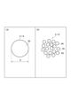
- the shapes of the first marker 6, the second marker 5, the third marker 8, and the fourth marker 7 are substantially spherical, and the cross section is substantially circular.
- FIG. 7(a) shows a case where each of the first marker 6, the second marker 5, the third marker 8, and the fourth marker 7 is mainly formed by a single void 9a.
- the void 9a is, for example, a vacuum hole or an air bubble.
- the diameter of the void 9a i.e., the diameter D of the first marker 6, the second marker 5, the third marker 8, and the fourth marker 7, is smaller than the width L (see FIG. 4) of the cross section of the optical waveguides 11 and 12.
- the width L of the optical waveguides 11 and 12 and the diameter D of the first marker 6, the second marker 5, the third marker 8, and the fourth marker 7 satisfy the following mathematical formula (1).
- the diameter D may be smaller than half the width L. That is, the width L and the diameter D may satisfy the following formula (2). D/L ⁇ 0.5...(2)
- FIG. 7(b) shows a case where each of the first marker 6, the second marker 5, the third marker 8, and the fourth marker 7 is a scatterer formed by scattering a plurality of minute voids 9b.
- Each of the plurality of voids 9b has a diameter of several tens to several hundreds of nanometers, for example, called a nanograting.
- the average density of each of the first marker 6, the second marker 5, the third marker 8, and the fourth marker 7 is, for example, 0.8 times or less the average density of the glass in the region of the glass substrate 1 excluding the optical waveguide portion 10, the first marker 6, the second marker 5, the third marker 8, and the fourth marker 7.
- the average density can be measured, for example, by STEM analysis.
- the fiber array 20 has a block portion 25, a fiber fixing portion 24, a cover portion 26, and a tape fiber 21.
- the block portion 25 has a rectangular parallelepiped shape.
- a V-groove 23 is provided on the surface facing the z direction in a region of the block portion 25 closer to the glass substrate 1 than the center of the block portion 25.
- the fiber fixing portion 24 has an approximately rectangular parallelepiped shape.
- the fiber fixing portion 24 is provided on the block portion 25 in a region closer to the glass substrate 1 than the center of the block portion 25.
- the cover portion 26 has a rectangular shape in a plan view. The upper surface of the cover portion 26 is curved in the xz plane.
- the cover portion 26 is provided on the block portion 25 on the opposite side to the glass substrate 1 with respect to the center of the block portion 25.
- the cover portion 26 is in contact with the fiber fixing portion 24.
- the tape fiber 21 is provided inside the cover portion 26 on the block portion 25.
- the tape fiber 21 includes a plurality of optical fibers 22.
- the portions of the optical fibers 22 extending from the tape fiber 21 are housed in the V-groove 23 and pressed against and fixed to the fiber fixing portion 24.
- Each of the optical fibers 22 is optically coupled to each of the optical waveguides 11 or each of the optical waveguides 12 at the end surface 3 of the glass substrate 1.
- the number of optical fibers 22 is the same as the total number of the optical waveguides 11 and the optical waveguides 12. As shown in FIG. 2, when the glass substrate 1 and the fiber array 20 are fixed to each other facing each other, the two first markers 6 are not covered by the fiber array 20 when viewed along the z direction. This makes the two first markers 6 visible from the z
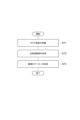
- FIG. 8 is a flowchart showing a method for manufacturing the optical module A.
- a glass substrate having a main surface 2 is prepared.
- a laser beam is irradiated into the interior of the glass substrate to form an optical waveguide section 10 including a plurality of optical waveguides 11 and a plurality of optical waveguides 12.
- the laser beam is irradiated by, for example, focusing laser beam from a femtosecond laser at a position where the optical waveguide section 10 is to be formed using a focusing optical system.
- the optical waveguide section 10 is formed by modifying the glass inside the glass substrate by multiphoton absorption caused by, for example, the irradiation of the femtosecond laser. Then, in step ST3, two first markers 6, a plurality of second markers 5, a plurality of third markers 8, and two fourth markers 7 are formed by irradiating the interior of the glass substrate 1 with laser beam.
- the laser light is irradiated by focusing, for example, laser light from a femtosecond laser at the intended positions for forming the first marker 6, the second marker 5, the third marker 8, and the fourth marker 7 using the same focusing optical system as in step ST2.
- the intensity (or power) of the laser light for forming the first marker 6, the second marker 5, the third marker 8, and the fourth marker 7 is greater than the intensity (or power) of the laser light for forming the multiple optical waveguides 11 and the multiple optical waveguides 12.
- the laser light for forming the first marker 6, the second marker 5, the third marker 8, and the fourth marker 7 may be laser light from a picosecond laser.
- step ST3 when forming the scatterers shown in FIG. 7(b) as the first marker 6, the second marker 5, the third marker 8, and the fourth marker 7, the condition for forming the scatterers is expressed by the following formula (3), where the softening point of the glass is T [K] and the power of the irradiated laser light is P [mW]. T/P ⁇ 15[K/mW]...(3) Alternatively, the condition for forming a scatterer may be expressed by the following equation (4). T/P ⁇ 13[K/mW]...(4)
- a plurality of markers (first marker 6, second marker 5, third marker 8, and fourth marker 7) that are marks indicating the positions of the optical waveguides 11 and 12 are provided inside the glass substrate 1. Since the relative positional relationship between the plurality of markers and the optical waveguides 11 and 12 is predetermined, the positions of the optical waveguides 11 and 12 formed inside the glass substrate 1 can be easily identified by visually checking the plurality of markers. This makes it possible to provide an optical waveguide substrate 1A that is easy to align each of the plurality of optical waveguides 11 and the plurality of optical waveguides 12 with each of the plurality of optical fibers 22 of the fiber array 20.
- the plurality of markers are provided at a fixed relative position in the thickness direction (z direction) of the glass substrate 1 with respect to the closest part of the optical waveguide section 10, it becomes easy to evaluate the relative positional relationship between the plurality of markers and the optical waveguides 11 and 12.
- the multiple markers are spaced apart from the optical waveguide section 10 when viewed along the thickness direction of the glass substrate 1, the multiple markers can be easily viewed from the thickness direction of the glass substrate 1.
- the multiple markers may be provided in an area close to the main surface 2 of the glass substrate 1 relative to the closest portion of the optical waveguide section 10.
- the intensity of the laser light when forming the multiple markers is made greater than the intensity of the laser light when forming the optical waveguides 11 and 12 in order to increase the visibility of the multiple markers.
- the multiple markers are formed using the same optical system as that used to form the optical waveguide section 10, the multiple markers are formed in an area close to the laser light incidence surface (i.e., the main surface 2) relative to the optical waveguide section 10 due to the difference in intensity of the laser light.
- the optical waveguides 11 and 12 and the multiple markers can be formed inside the glass substrate 1 without changing the optical system. This simplifies the process of forming the optical waveguides 11 and 12 and the multiple markers.
- each of the multiple markers may be formed mainly by holes 9a (or 9b).
- This increases the difference in refractive index between the glass constituting the glass substrate 1 and the multiple markers. This improves the visibility of the multiple markers, making it easier to identify the positions of the optical waveguides 11 and 12.
- the diameter D of the holes 9a may be smaller than the width L of the cross section of the optical waveguides 11 and 12. This improves the accuracy of identifying the positions of the multiple markers. Therefore, the accuracy of identifying the positions of the optical waveguides 11 and 12 is improved.
- the multiple markers When each of the multiple markers is mainly formed by voids 9a (or 9b) as in this embodiment, the multiple markers may be 10 ⁇ m or more away from the optical waveguide section 10.
- the stress caused by the voids 9a (or 9b) may affect the optical propagation characteristics of the optical waveguide section 10.
- the effect of the stress caused by the voids 9a (or 9b) on the optical propagation characteristics of the optical waveguide section 10 can be reduced.
- the multiple markers by providing the multiple markers at a position 10 ⁇ m or more away from the optical waveguide section 10, the multiple markers can be separated from the area where crosstalk of the optical waveguide section 10 may occur.
- the glass substrate 1 may have an end surface 3 and an end surface 4.
- the optical waveguide section 10 may include an optical waveguide 11.
- the optical waveguide 11 may have an end 11a in a region close to the end surface 3 and an end 11b in a region close to the end surface 4.
- the multiple markers may include a first marker 6 that is a mark indicating the position of the end 11a and a second marker 5 that is a mark indicating the position of the end 11b.
- the position of the end 11a in the thickness direction (z direction) of the glass substrate 1 may be different from the position of the end 11b in the thickness direction.
- the relative position of the first marker 6 in the thickness direction of the glass substrate 1 with respect to the end 11a may be the same as the relative position of the second marker 5 in the thickness direction with respect to the end 11b. Even for such an optical waveguide 11 in which the positions of both ends 11a and 11b in the thickness direction of the glass substrate 1 are different from each other, the positions of each end 11a and 11b can be easily identified by the first marker 6 and the second marker 5.
- the multiple markers may further include a third marker 8 that is a mark indicating the position of the end 11b.
- the optical waveguide 11 When viewed along the thickness direction (z direction) of the glass substrate 1, the optical waveguide 11 may be located between the second marker 5 and the third marker 8. The end 11b may be present inside the glass substrate 1. In this way, by positioning the optical waveguide 11 between the second marker 5 and the third marker 8, the position of the end 11b can be more easily identified. In addition, it is difficult to visually recognize the optical waveguides 11 and 12, especially when the end 11b of the optical waveguide 11 and the end 12b of the optical waveguide 12 are present inside the glass substrate 1.
- the distance W1 between the end 11b and the second marker 5 in the extension direction (x direction) of the optical waveguide 11 is equal to the distance W2 between the end 11b and the third marker 8 in the extension direction of the optical waveguide 11.
- the distance W3 between the end 12b and the first fourth marker 7 in the extension direction (x direction) of the optical waveguide 12 is equal to the distance W4 between the end 12b and the second fourth marker 7 in the extension direction of the optical waveguide 12.
- each of the multiple markers may be a scatterer formed by scattering multiple voids 9b. Scattering of the voids 9b in the scatterer, i.e., multiple voids 9b being densely dispersed, scatters light and improves the visibility of the multiple markers. Therefore, the positions of the optical waveguides 11, 12 inside the glass substrate 1 can be more easily identified. In addition, by providing multiple voids 9b with small diameters, the accuracy of the formation position of the multiple markers is improved compared to the case of providing a single void 9a with a large diameter.
- the average density of each of the multiple markers may be 0.8 times or less the average density of the glass in the area of the glass substrate 1 excluding the optical waveguide section 10 and the multiple markers. In this case, the visibility of the scatterer is further improved. Therefore, the positions of the optical waveguides 11, 12 inside the glass substrate 1 can be more easily identified.
- the first marker 6 inside the glass substrate 1 is not covered by the fiber array 20. Therefore, when the fiber array 20 is placed at a predetermined fixed position relative to the glass substrate 1, the first marker 6 inside the glass substrate 1 can be viewed without being obstructed by the fiber array 20. This makes it easy to align the optical axes of the glass substrate 1 and the fiber array 20.
- a laser beam is irradiated inside the glass substrate to form a plurality of markers that indicate the positions of the optical waveguide section 10 and the optical waveguides 11 and 12.
- the plurality of markers can be easily formed together with the optical waveguide section 10 that is also formed by irradiating the laser beam.
- the intensity of the laser light in step ST3, which forms the multiple markers may be greater than the intensity of the laser light in step ST2, which forms the optical waveguide portion 10.
- multiple markers that are mainly formed by the voids 9a or are scatterers formed by scattering the multiple voids 9b can be formed inside the glass substrate.
- the first marker 6, the second marker 5, the third marker 8, and the fourth marker 7 are provided in a region close to the main surface 2 (one of the plate surfaces) with respect to the optical waveguide portion 10.
- the present invention is not limited to this embodiment, and the positions of the first marker 6, the second marker 5, the third marker 8, and the fourth marker 7 may be the same as the positions of the nearest parts of the optical waveguide portion 10 in the z direction.
- the positions of the center lines of the optical waveguides 11 and 12 and the center points of the multiple markers in the z direction may be the same. This makes it possible to avoid the need to consider the difference in the positions of the multiple markers and the optical waveguides 11 and 12 in the thickness direction of the glass substrate 1. This makes it easy to evaluate the relative positional relationship between the multiple markers and the optical waveguides 11 and 12.
- the optical waveguide section 10 may be formed by, for example, an ion exchange method.
- the optical waveguide section 10 and the multiple markers can be formed by the same device.
- the accuracy of the formation position of the multiple markers relative to the optical waveguide section 10 can be improved. Therefore, the accuracy of identifying the position of the optical waveguide section 10 can be further improved.
- the present disclosure has been specifically described above based on the embodiments, the present disclosure is not limited to the above embodiments and can be modified within the scope of the present disclosure.
- an example is shown in which a plurality of second markers 5 and a plurality of third markers 8 are provided, but a single second marker 5 and a single third marker 8 may be provided.
- the first marker 6 and the fourth marker 7 are not limited to the above embodiments, and a plurality of markers may be formed so as to be aligned in the x direction, like the second marker 5 and the third marker 8.
- the optical waveguide section 10 includes a plurality of optical waveguides 11 and a plurality of optical waveguides 12, but the optical waveguide section 10 may include only one of the optical waveguides 11 and the optical waveguide 12, or both.
Landscapes
- Physics & Mathematics (AREA)
- General Physics & Mathematics (AREA)
- Optics & Photonics (AREA)
- Engineering & Computer Science (AREA)
- Microelectronics & Electronic Packaging (AREA)
- Optical Integrated Circuits (AREA)
Abstract
光導波路基板(1A)は、ガラス基板(1)を備える。ガラス基板(1)は、ガラス基板(1)の内部に形成された一または複数の光導波路(11、12)を含む光導波路部(10)と、ガラス基板(1)の内部に形成された、一または複数の光導波路(11、12)の位置を示す目印である複数のマーカー(5、6、7、8)と、を有する。複数のマーカー(5、6、7、8)は、光導波路部(10)の最も近い部分に対してガラス基板(1)の厚み方向(z方向)に一定の相対位置に設けられ、厚み方向(z方向)に沿って見て光導波路部(10)から離れている。
Description
本開示は、光導波路基板、光学モジュール、および光導波路基板の製造方法に関する。本出願は、2023年7月5日出願の日本出願第2023-110707号に基づく優先権を主張し、前記日本出願に記載された全ての記載内容を援用する。
特許文献1には、線形光学特性および非線形光学特性を有する透明結晶基板の中に、光導波路を形成する方法が開示されている。この方法は、線形光学特性を有する第1の基板にフェムト秒レーザを照射して第1の光導波路を形成する工程と、第1の光導波路が形成された第1の基板と非線形光学特性を有する第2の基板とを接合する位置をアラインメントする工程と、アラインメントされた第1の基板と第2の基板とを接合して、透明結晶基板を形成する工程とを含む。
本開示の一実施形態による光導波路基板は、ガラス基板を備える。ガラス基板は、ガラス基板の内部に形成された一または複数の光導波路を含む光導波路部と、ガラス基板の内部に設けられた、一または複数の光導波路の位置を示す目印である複数のマーカーと、を有する。複数のマーカーは、光導波路部の最も近い部分に対してガラス基板の厚み方向に一定の相対位置に設けられ、厚み方向に沿って見て光導波路部から離れている。
[本開示が解決しようとする課題]
ガラス基板の内部に、光導波路が形成される場合がある。しかしながら、ガラス基板と光導波路との屈折率差は小さいので、光導波路を視認することは難しい。したがって、光導波路の位置を効率的に特定することができず、光導波路と、光導波路に接続される光学部品との接続における調心に時間がかかるという問題がある。
ガラス基板の内部に、光導波路が形成される場合がある。しかしながら、ガラス基板と光導波路との屈折率差は小さいので、光導波路を視認することは難しい。したがって、光導波路の位置を効率的に特定することができず、光導波路と、光導波路に接続される光学部品との接続における調心に時間がかかるという問題がある。
[本開示の効果]
本開示によれば、ガラス基板の内部に形成された光導波路の位置を容易に特定可能な光導波路基板、光学モジュール、および光導波路基板の製造方法を提供できる。
本開示によれば、ガラス基板の内部に形成された光導波路の位置を容易に特定可能な光導波路基板、光学モジュール、および光導波路基板の製造方法を提供できる。
[本開示の実施形態の説明]
最初に、本開示の実施形態の内容を列記して説明する。
最初に、本開示の実施形態の内容を列記して説明する。
[1]本開示の一実施形態による光導波路基板は、ガラス基板を備える。ガラス基板は、ガラス基板の内部に形成された一または複数の光導波路を含む光導波路部と、ガラス基板の内部に設けられた、一または複数の光導波路の位置を示す目印である複数のマーカーと、を有する。複数のマーカーは、光導波路部の最も近い部分に対してガラス基板の厚み方向に一定の相対位置に設けられ、厚み方向に沿って見て光導波路部から離れている。
光導波路の位置を示す目印である複数のマーカーがガラス基板の内部に設けられる。複数のマーカーと光導波路との相対位置関係は予め定まっているので、複数のマーカーを視認することにより、ガラス基板の内部に形成された光導波路の位置を容易に特定することができる。加えて、複数のマーカーが、光導波路部の最も近い部分に対してガラス基板の厚み方向に一定の相対位置に設けられることにより、複数のマーカーと光導波路との相対位置関係の評価が容易となる。加えて、複数のマーカーが、ガラス基板の厚み方向に沿って見て光導波路部から離れていることにより、ガラス基板の厚み方向から複数のマーカーを容易に視認することができる。
[2]上記[1]の光導波路基板において、複数のマーカーは、光導波路部の最も近い部分に対してガラス基板の厚み方向を向く一方の板面に近い領域に設けられてもよい。ガラス基板の内部に複数のマーカーおよび光導波路をレーザ光の照射により形成する場合、複数のマーカーの視認性を高めるため、複数のマーカーを形成する際のレーザ光の強度は、光導波路を形成する際のレーザ光の強度よりも大きくされる。加えて、光導波路を形成する際に用いる光学系と同一の光学系を用いて複数のマーカーを形成する場合、レーザ光の強度の違いにより、複数のマーカーは光導波路に対してレーザ光入射面に近い領域に形成される。言い換えると、複数のマーカーが光導波路部の最も近い部分に対してガラス基板の一方の板面に近い領域に設けられることにより、光学系を変更せずに光導波路と複数のマーカーとを形成することができる。これにより、光導波路および複数のマーカーを形成する工程を簡略化できる。
[3]上記[1]の光導波路基板において、ガラス基板の厚み方向における複数のマーカーの位置は光導波路部の最も近い部分の位置と同じであってもよい。これにより、ガラス基板の厚み方向における複数のマーカーと光導波路との位置の違いを考慮せずに済む。したがって、複数のマーカーと光導波路との相対位置関係の評価が容易となる。
[4]上記[1]から[3]のいずれか1つの光導波路基板において、複数のマーカーのそれぞれは、空孔により主に形成されてもよい。これにより、ガラス基板を構成するガラスと複数のマーカーとの屈折率差が大きくなる。よって、複数のマーカーの視認性が向上するので、光導波路の位置を更に容易に特定することができる。
[5]上記[4]の光導波路基板において、空孔の直径は、各第1光導波路の横断面の幅よりも小さくてもよい。これにより、複数のマーカーの位置の特定精度が向上する。したがって、光導波路の位置の特定精度が向上する。
[6]上記[1]から[3]のいずれか1つの光導波路基板において、複数のマーカーのそれぞれは、複数の空孔が散乱して形成された散乱体であってもよい。散乱体における空孔の散乱によって、複数のマーカーの視認性が向上する。したがって、ガラス基板の内部における光導波路の位置を更に容易に特定することができる。加えて、直径の小さな空孔を複数設けることにより、直径の大きな単一の空孔を設ける場合と比較して、複数のマーカーの形成位置の精度が向上する。
[7]上記[6]の光導波路基板において、複数のマーカーのそれぞれの平均密度は、ガラス基板のうち光導波路部および複数のマーカーを除く領域のガラスの平均密度の0.8倍以下であってもよい。この場合、散乱体の視認性がより向上する。したがって、ガラス基板の内部における光導波路の位置を更に容易に特定することができる。
[8]上記[4]から[7]のいずれか1つの光導波路基板において、複数のマーカーは、光導波路部から10μm以上離れていてもよい。複数のマーカーのそれぞれが、空孔により主に形成されるか、または複数の空孔で形成された散乱体である場合、空孔により生じる応力が光導波路部の光伝搬特性に影響を与えるおそれがある。複数のマーカーが、光導波路部から10μm以上離れた位置に設けられることにより、空孔により生じる応力が光導波路部の光伝搬特性に与える影響を低減できる。
[9]上記[1]から[8]のいずれか1つの光導波路基板において、ガラス基板は第1端面および第2端面を有してもよい。光導波路部は第1光導波路を含んでもよい。第1光導波路は、第1端面に近い領域の第1端部と、第2端面に近い領域の第2端部とを有してもよい。複数のマーカーは、第1端部の位置を示す目印である第1マーカーと、第2端部の位置を示す目印である第2マーカーとを含んでもよい。ガラス基板の厚み方向における第1端部の位置は、厚み方向における第2端部の位置と異なってもよい。第1端部に対する、ガラス基板の厚み方向における第1マーカーの相対位置は、第2端部に対する、厚み方向における第2マーカーの相対位置と同一であってもよい。このような、ガラス基板の厚み方向における両端部の位置が互いに異なる光導波路に対しても、第1マーカーおよび第2マーカーによって各端部の位置を容易に特定することができる。
[10]上記[9]の光導波路基板において、複数のマーカーは、第2端部の位置を示す目印である第3マーカーを更に含んでもよい。ガラス基板の厚み方向に沿って見て、第1光導波路は第2マーカーと第3マーカーとの間に位置してもよい。第2端部はガラス基板の内部に存在してもよい。第1光導波路の延びる方向における第2端部と第2マーカーとの距離は、第1光導波路の延びる方向における第2端部と第3マーカーとの距離と等しくてもよい。このように、第1光導波路が第2マーカーと第3マーカーとの間に位置することにより、第2端部の位置を更に容易に特定することができる。加えて、光導波路の端部がガラス基板の内部に存在する場合には特に、光導波路を視認しづらい。第1光導波路の延びる方向における第2端部と第2マーカーとの距離が、第1光導波路の延びる方向における第2端部と第3マーカーとの距離と等しいことによって、第2端部がガラス基板の内部に存在する場合であっても、第2端部の位置を容易に特定することができる。
[11]本開示の一実施形態による光学モジュールは、上記[1]から[10]のうちいずれか一つの光導波路基板と、光導波路部と光学的に結合される光学部品とを備える。ガラス基板は、第1端面を有する。光導波路部は第1光導波路を含む。第1光導波路は、第1端面に近い領域の第1端部を有する。光学部品は第1端面において第1光導波路と光学的に結合される。複数のマーカーは、第1端部の位置を示す目印である第1マーカーを含む。厚み方向に沿って見て、第1マーカーは光学部品によって覆われない。この光学モジュールによれば、光学部品をガラス基板に対して所定の固定位置に配置した状態において、ガラス基板の内部にある第1マーカーを光学部品に妨げられることなく視認することができる。したがって、ガラス基板と光学部品との光軸合わせが容易となる。
[12]本開示の一実施形態による光導波路基板の製造方法は、ガラス基板の内部にレーザ光を照射することにより、一または複数の光導波路を含む光導波路部を形成する工程と、ガラス基板の内部にレーザ光を照射することにより、一または複数の光導波路の位置を示す目印である複数のマーカーを形成する工程と、を含む。複数のマーカーは、光導波路部の最も近い部分に対してガラス基板の厚み方向に一定の相対位置に形成される。複数のマーカーは、ガラス基板の厚み方向に沿って見て光導波路部から離れている。複数のマーカーのそれぞれは、空孔により主に形成されるか、または複数の空孔が散乱して形成された散乱体である。
この製造方法によれば、ガラス基板の内部にレーザ光を照射することにより、光導波路部、および光導波路の位置を示す目印である複数のマーカーが形成される。複数のマーカーと光導波路との相対位置関係は予め定まっているので、複数のマーカーを視認することにより、ガラス基板の内部に形成された光導波路の位置を容易に特定することができる。加えて、複数のマーカーが、光導波路部の最も近い部分に対してガラス基板の厚み方向に一定の相対位置に設けられることにより、複数のマーカーと光導波路との相対位置関係の評価が容易となる。加えて、複数のマーカーが、ガラス基板の厚み方向に沿って見て光導波路部から離れていることにより、ガラス基板の厚み方向から複数のマーカーを容易に視認することができる。加えて、空孔により主に形成されるか、または複数の空孔が散乱して形成された散乱体である複数のマーカーをレーザ光の照射により形成することによって、同じくレーザ光の照射により形成される光導波路部とともに、複数のマーカーを容易に形成することができる。
[13]上記[12]の製造方法において、複数のマーカーを形成する工程におけるレーザ光の強度は、光導波路部を形成する工程におけるレーザ光の強度よりも大きくてもよい。例えばこのような方法によって、空孔により主に形成されるか、または複数の空孔が散乱して形成された散乱体である複数のマーカーを、ガラス基板の内部に形成することができる。
[本開示の実施形態の詳細]
本開示の光導波路基板、光学モジュール、および光導波路基板の製造方法の具体例を、以下に図面を参照しつつ説明する。なお、本開示はこれらの例示に限定されるものではなく、請求の範囲によって示され、請求の範囲と均等の意味および範囲内でのすべての変更が含まれることが意図される。以下の説明では、図面の説明において同一の要素には同一の符号を付し、重複する説明を省略する。
本開示の光導波路基板、光学モジュール、および光導波路基板の製造方法の具体例を、以下に図面を参照しつつ説明する。なお、本開示はこれらの例示に限定されるものではなく、請求の範囲によって示され、請求の範囲と均等の意味および範囲内でのすべての変更が含まれることが意図される。以下の説明では、図面の説明において同一の要素には同一の符号を付し、重複する説明を省略する。
(実施形態)
図1は、本開示の実施形態に係る光学モジュールAを示す斜視図である。図2は、光学モジュールAを示す平面図である。図3は、光学モジュールAを示す側面図である。光学モジュールAは、光導波路基板1Aとファイバアレイ20(光学部品)とを備える。光導波路基板1Aは、ガラス基板1を有する。ガラス基板1は、ファイバアレイ20とx方向に向かい合ってファイバアレイ20に固定されている。ガラス基板1の形状は、平板状である。ガラス基板1は、平面視にて長方形の形状を有している。ガラス基板1の材料としては、1100nm以上1650nm以下の波長の光の、厚さ0.5cmの基板における透過率が90%以上であるガラスを好適に用いることができる。このようなガラスとしては、合成石英ガラス、ボロシリケートガラス、アルミノシリケートガラス、およびアルカリシリケートガラスが例示される。ガラス基板1は、主面2と、端面3(第1端面)と、端面4(第2端面)と、光導波路部10と、複数のマーカーとを含む。複数のマーカーは、2つの第1マーカー6と、複数の第2マーカー5と、複数の第3マーカー8と、2つの第4マーカー7とを含む。
図1は、本開示の実施形態に係る光学モジュールAを示す斜視図である。図2は、光学モジュールAを示す平面図である。図3は、光学モジュールAを示す側面図である。光学モジュールAは、光導波路基板1Aとファイバアレイ20(光学部品)とを備える。光導波路基板1Aは、ガラス基板1を有する。ガラス基板1は、ファイバアレイ20とx方向に向かい合ってファイバアレイ20に固定されている。ガラス基板1の形状は、平板状である。ガラス基板1は、平面視にて長方形の形状を有している。ガラス基板1の材料としては、1100nm以上1650nm以下の波長の光の、厚さ0.5cmの基板における透過率が90%以上であるガラスを好適に用いることができる。このようなガラスとしては、合成石英ガラス、ボロシリケートガラス、アルミノシリケートガラス、およびアルカリシリケートガラスが例示される。ガラス基板1は、主面2と、端面3(第1端面)と、端面4(第2端面)と、光導波路部10と、複数のマーカーとを含む。複数のマーカーは、2つの第1マーカー6と、複数の第2マーカー5と、複数の第3マーカー8と、2つの第4マーカー7とを含む。
主面2は、ガラス基板1の厚み方向を向く一方の板面であり、x方向およびx方向と交差するy方向に沿ったガラス基板1の表面である。主面2の法線方向は、ガラス基板1の厚み方向と一致する。ここでは、ガラス基板1の厚み方向をz方向と定義する。端面3は、y方向およびz方向に沿ったガラス基板1の表面である。端面3は、主面2に連続しており、主面2に対して例えば垂直に設けられている。端面3において、ガラス基板1とファイバアレイ20とが互いに向かい合っている。端面4は、端面3に対してファイバアレイ20とは反対側のガラス基板1の表面である。端面4は、主面2に連続しており、主面2に対して傾斜を有している。端面4の法線ベクトルは、z方向の正方向を向く成分を含んでいる。主面2、端面3および端面4は、例えば平坦である。
光導波路部10は、複数の光導波路11(第1光導波路)と、複数の光導波路12(第2光導波路)とを含む。複数の光導波路11および複数の光導波路12は、例えば多光子吸収によってガラスが変質した高屈折率領域である。光導波路部10の延びる方向は、端面3および端面4の双方と交差している。光導波路部10の延びる方向は、主にx方向である。複数の光導波路11は、ガラス基板1の内部に設けられており、y方向に並んで設けられている。図3に示されるように、各光導波路11は、領域aと、領域bと、領域cとを含む。領域aは、各光導波路11の中央部よりも端面4に近い領域である。領域aにおいて、複数の光導波路11は主面2に沿ってx方向に延びており、y方向に並んで設けられている。領域bは、複数の光導波路11の中央部の領域である。領域bにおいて、複数の光導波路11は湾曲しており、y方向に並んで設けられている。領域cは、複数の光導波路11の領域bよりも端面3に近い領域である。複数の光導波路11の領域cは、領域aと比較して、主面2から離れている。複数の光導波路11の領域cは、x方向に延びており、y方向に並んで設けられている。複数の光導波路12は、ガラス基板1の内部に設けられており、y方向に並んで設けられている。複数の光導波路12は、全体にわたって主面2と平行にx方向に延びている。複数の光導波路12は、光導波路11の領域aと比較して、主面2から離れて設けられている。複数の光導波路11の領域cと複数の光導波路12とは、z方向に沿って見て交互にy方向に並んでいる。
端面3付近における光導波路11と、光導波路11と隣り合う光導波路12との間隔は、端面4付近における光導波路11と、光導波路11と隣り合う別の光導波路11との間隔、および、光導波路12と、光導波路12と隣り合う別の光導波路12との間隔と等しい。端面3に近い領域の複数の光導波路11の端部11a(第1端部)のz方向の位置は、端面3に近い領域の(図示例では端面3に含まれる)複数の光導波路12の端部12aのz方向の位置と同一である。図示例では端部11a,12aは端面3に含まれてガラス基板1から露出しているが、端部11a,12aは端面3から離れてガラス基板1の内部に位置してもよい。端面4に近い領域の複数の光導波路11の端部11b(第2端部)のz方向の位置は、端面4に近い領域の複数の光導波路12の端部12bのz方向の位置と異なっている。図示例では端部11b,12bは端面4から離れているが、端部11b,12bは端面4に含まれてガラス基板1から露出してもよい。端面4付近において、複数の光導波路11の端部11bは、複数の光導波路12の端部12bよりも主面2に近い。
図4は、各光導波路11および各光導波路12の横断面、すなわち各光導波路11および各光導波路12が延びる方向に垂直な断面を模式的に示す図である。ガラス基板1のガラスに対する各光導波路11および各光導波路12の比屈折率差は、例えば0.2%以上0.5%以下である。図4(a)に示すように、各光導波路11および各光導波路12の断面形状が正方形である場合、各光導波路11および各光導波路12の断面の一辺の長さは、例えば3μm以上7.5μm以下である。図4(b)に示すように、各光導波路11および各光導波路12の断面形状が円形である場合、各光導波路11および各光導波路12の断面の直径は、例えば4μm以上9μm以下である。
再度図1から図3を参照する。2つの第1マーカー6と、複数の第2マーカー5と、複数の第3マーカー8と、2つの第4マーカー7とは、ガラス基板1の内部に設けられた、複数の光導波路11および複数の光導波路12の位置を示す目印である。2つの第1マーカー6と、複数の第2マーカー5と、複数の第3マーカー8と、2つの第4マーカー7とは、光導波路部10の最も近い部分に対してz方向に一定の相対位置に設けられ(すなわちz方向における光導波路部10との距離が均一であり)、z方向に沿って見て光導波路部10から離れている。図示例において、2つの第1マーカー6と、複数の第2マーカー5と、複数の第3マーカー8と、2つの第4マーカー7とは、光導波路部10の最も近い部分に対して主面2に近い領域に設けられている。
図5は、ガラス基板1の端面4付近を示す拡大平面図である。複数の第2マーカー5および複数の第3マーカー8は、複数の光導波路11の端部11bの位置を示す目印である。複数の第2マーカー5および複数の第3マーカー8は、ガラス基板1の内部において、複数の光導波路11の領域aの近傍に設けられている。図5に示すように、複数の第2マーカー5は、z方向に沿って見て、光導波路部10の延びる方向(x方向)と交差する方向(y方向)に光導波路部10から離れており、x方向に沿って並んで設けられている。複数の第3マーカー8は、z方向に沿って見て、光導波路部10の延びる方向(x方向)と交差する方向(y方向)に光導波路部10から離れており、x方向に沿って並んで設けられている。z方向に沿って見て、複数の光導波路11は、複数の第2マーカー5のみからなる群と、複数の第3マーカー8のみからなる群との間に位置する。ここで、複数の光導波路11の端部11bを通り、y軸に平行な架空の直線S1を想定する。複数の第2マーカー5のうち最も端面4に近い領域の第2マーカー5と、直線S1との距離W1は、複数の第3マーカー8のうち最も端面4に近い領域の第3マーカー8と、直線S1との距離W2と等しい。言い換えると、光導波路11の延びる方向(x方向)における端部11bと第2マーカー5との距離は、同方向における端部11bと第3マーカー8との距離と等しい。
図6は、図1に示されるVI-VI線に沿った部分断面図である。図6に示すように、複数の第2マーカー5と、光導波路部10のうち複数の第2マーカー5に最も近い光導波路11との距離D1は10μm以上である。同様に、複数の第3マーカー8と、光導波路部10のうち複数の第3マーカー8に最も近い光導波路11との距離D2は10μm以上である。第1マーカー6および第4マーカー7についても同様である。また、前述したように、第2マーカー5および第3マーカー8は、光導波路部10の最も近い部分に対して主面2に近い領域に設けられている。言い換えると、第2マーカー5および第3マーカー8の中心は、光導波路11の中心に対して距離W5だけ主面2に近い領域に位置している。距離W5の大きさは、例えば3μm以上10μm以下である。第1マーカー6および第4マーカー7についても同様である。すなわち、マーカーと、マーカーに最も近い光導波路との距離は、所定の距離にある。
図2および図3に示すように、2つの第1マーカー6は、ガラス基板1の内部において、ガラス基板1の中央部よりも端面3に近い領域に設けられている。2つの第1マーカー6は、複数の光導波路11の端部11a、および複数の光導波路12の端部12aの位置を示す目印である。2つの第1マーカー6は、z方向に沿って見て、光導波路部10の延びる方向(x方向)と交差する方向(y方向)に光導波路部10から離れて設けられている。z方向に沿って見て、複数の光導波路11および複数の光導波路12は、第1の第1マーカー6と、第2の第1マーカー6との間に位置する。端部11a,12aに対する、z方向における第1マーカー6の相対位置は、端部11b,12bに対する、z方向における第2マーカー5の相対位置と同一である。すなわち、z方向における端部11a,12aと第1マーカー6との距離は、z方向における端部11b,12bと第2マーカー5との距離と等しい。端面3から第1の第1マーカー6までの距離は、端面3から第2の第1マーカー6までの距離と等しい。
図5に示すように、2つの第4マーカー7は、ガラス基板1の内部において、ガラス基板1の中央部よりも端面4に近い領域に設けられている。2つの第4マーカー7は、複数の光導波路12の端部12bの位置を示す目印である。2つの第4マーカー7は、z方向に沿って見て、光導波路部10の延びる方向(x方向)と交差する方向(y方向)に光導波路部10(より具体的には複数の光導波路12)から離れて設けられている。z方向に沿って見て、複数の光導波路12は、第1の第4マーカー7と、第2の第4マーカー7との間に位置する。ここで、複数の光導波路12の端部12bを通り、y軸に平行な架空の直線S2を想定する。第1の第4マーカー7と、直線S2との距離W3は、第2の第4マーカー7と、直線S2との距離W4と等しい。言い換えると、光導波路12の延びる方向(x方向)における端部12bと第4マーカー7との距離は、全ての第4マーカー7において均一である。
図7は、第1マーカー6、第2マーカー5、第3マーカー8、および第4マーカー7の断面を模式的に示す図である。第1マーカー6、第2マーカー5、第3マーカー8、および第4マーカー7の形状は、略球状であり、断面形状は略円形である。図7(a)は、第1マーカー6、第2マーカー5、第3マーカー8、および第4マーカー7のそれぞれが、単一の空孔9aにより主に形成されている場合を示す。空孔9aは、例えば真空孔または気泡である。空孔9aの直径すなわち第1マーカー6、第2マーカー5、第3マーカー8、および第4マーカー7の直径Dは、光導波路11,12の横断面の幅L(図4を参照)よりも小さい。すなわち、光導波路11,12の幅Lと、第1マーカー6、第2マーカー5、第3マーカー8、および第4マーカー7の直径Dとは、次の数式(1)を満たす。
D/L<1 ・・・(1)
或いは、直径Dは、幅Lの半分よりも小さくてもよい。すなわち、幅Lと直径Dとは、次の数式(2)を満たしてもよい。
D/L<0.5 ・・・(2)
D/L<1 ・・・(1)
或いは、直径Dは、幅Lの半分よりも小さくてもよい。すなわち、幅Lと直径Dとは、次の数式(2)を満たしてもよい。
D/L<0.5 ・・・(2)
図7(b)は、第1マーカー6、第2マーカー5、第3マーカー8、および第4マーカー7のそれぞれが、複数の微小な空孔9bが散乱して形成された散乱体である場合を示す。複数の空孔9bのそれぞれは、例えばナノグレーティングと呼ばれる、数十ナノメートルから数百ナノメートルの直径を有する。その場合、第1マーカー6、第2マーカー5、第3マーカー8、および第4マーカー7のそれぞれの平均密度は、ガラス基板1のうち光導波路部10、第1マーカー6、第2マーカー5、第3マーカー8、および第4マーカー7を除く領域のガラスの平均密度の例えば0.8倍以下である。平均密度は、例えばSTEM分析によって測定可能である。
再び図1から図3を参照する。ファイバアレイ20は、ブロック部25と、ファイバ固定部24と、カバー部26と、テープファイバ21とを有する。ブロック部25は、直方体の形状を有している。ブロック部25の中央部よりもガラス基板1に近い領域の、z方向を向く面上には、V溝23が設けられている。ファイバ固定部24は、略直方体の形状を有している。ファイバ固定部24は、ブロック部25の中央部よりもガラス基板1に近い領域のブロック部25上に設けられている。カバー部26は、平面視にて長方形の形状を有している。カバー部26の上面は、xz平面において湾曲している。カバー部26は、ブロック部25の中央部に対してガラス基板1とは反対側のブロック部25上に設けられている。カバー部26は、ファイバ固定部24と接触している。テープファイバ21は、ブロック部25上のカバー部26の内部に設けられている。テープファイバ21は、複数の光ファイバ22を含む。テープファイバ21から延出する複数の光ファイバ22の部分は、V溝23に収容されつつ、ファイバ固定部24に押しつけられて固定されている。複数の光ファイバ22のそれぞれは、ガラス基板1の端面3において複数の光導波路11のそれぞれまたは複数の光導波路12のそれぞれと光学的に結合している。光ファイバ22の数は、複数の光導波路11および複数の光導波路12を合わせた数と同一である。図2に示すように、ガラス基板1とファイバアレイ20とが向かい合って互いに固定された状態において、z方向に沿って見て2つの第1マーカー6はファイバアレイ20によって覆われていない。これにより、2つの第1マーカー6はz方向から視認可能とされている。
本開示の第1実施形態に係る光学モジュールAの製造方法について説明する。図8は、光学モジュールAの製造方法を示すフローチャートである。まず、工程ST1において、主面2を有するガラス基板を準備する。次に、工程ST2において、ガラス基板の内部にレーザ光を照射することにより、複数の光導波路11および複数の光導波路12を含む光導波路部10を形成する。レーザ光の照射は、例えばフェムト秒レーザからのレーザ光を、集光光学系により光導波路部10の形成予定位置に集光することにより行われる。光導波路部10は、例えばフェムト秒レーザの照射により生じる多光子吸収によって、ガラス基板内部のガラスが改質されることにより形成される。その後、工程ST3において、ガラス基板1の内部にレーザ光を照射することにより、2つの第1マーカー6、複数の第2マーカー5、複数の第3マーカー8、および2つの第4マーカー7を形成する。レーザ光の照射は、例えばフェムト秒レーザからのレーザ光を、工程ST2と同一の集光光学系により第1マーカー6、第2マーカー5、第3マーカー8、および第4マーカー7の形成予定位置に集光することにより行われる。このとき、第1マーカー6、第2マーカー5、第3マーカー8、および第4マーカー7を形成するためのレーザ光の強度(またはパワー)は、複数の光導波路11および複数の光導波路12を形成するためのレーザ光の強度(またはパワー)よりも大きい。第1マーカー6、第2マーカー5、第3マーカー8、および第4マーカー7を形成するためのレーザ光は、ピコ秒レーザからのレーザ光であってもよい。
工程ST3において、第1マーカー6、第2マーカー5、第3マーカー8、および第4マーカー7として図7(b)に示された散乱体を形成する場合、散乱体が形成される条件は、ガラスの軟化点をT[K]、照射するレーザ光のパワーをP[mW]としたとき、次の数式(3)によって表される。
T/P<15[K/mW] ・・・(3)
或いは、散乱体が形成される条件は、次の数式(4)によって表されてもよい。
T/P<13[K/mW] ・・・(4)
T/P<15[K/mW] ・・・(3)
或いは、散乱体が形成される条件は、次の数式(4)によって表されてもよい。
T/P<13[K/mW] ・・・(4)
以上の構成を備える光学モジュールAおよび光学モジュールAの製造方法から得られる効果について説明する。本実施形態では、光導波路11,12の位置を示す目印である複数のマーカー(第1マーカー6、第2マーカー5、第3マーカー8、および第4マーカー7)がガラス基板1の内部に設けられる。複数のマーカーと光導波路11,12との相対位置関係は予め定まっているので、複数のマーカーを視認することにより、ガラス基板1の内部に形成された光導波路11,12の位置を容易に特定することができる。これにより、複数の光導波路11および複数の光導波路12のそれぞれと、ファイバアレイ20の複数の光ファイバ22のそれぞれとの調心が容易な光導波路基板1Aを提供できる。加えて、複数のマーカーが、光導波路部10の最も近い部分に対してガラス基板1の厚み方向(z方向)に一定の相対位置に設けられることにより、複数のマーカーと光導波路11,12との相対位置関係の評価が容易となる。加えて、複数のマーカーが、ガラス基板1の厚み方向に沿って見て光導波路部10から離れていることにより、ガラス基板1の厚み方向から複数のマーカーを容易に視認することができる。
本実施形態のように、複数のマーカーは、光導波路部10の最も近い部分に対してガラス基板1の主面2に近い領域に設けられてもよい。ガラス基板1の内部に複数のマーカーおよび光導波路11,12をレーザ光の照射により形成する場合、複数のマーカーの視認性を高めるため、複数のマーカーを形成する際のレーザ光の強度は、光導波路11,12を形成する際のレーザ光の強度よりも大きくされる。更に、光導波路部10を形成する際に用いる光学系と同一の光学系を用いて複数のマーカーを形成する場合、レーザ光の強度の違いにより、複数のマーカーは光導波路部10に対してレーザ光入射面(すなわち主面2)に近い領域に形成される。言い換えると、複数のマーカーを光導波路部10の最も近い部分に対して主面2に近い領域に形成することにより、光学系を変更せずに光導波路11,12と複数のマーカーとをガラス基板1の内部に形成することができる。これにより、光導波路11,12および複数のマーカーを形成する工程を簡略化できる。
本実施形態のように、複数のマーカーのそれぞれは、空孔9a(または9b)により主に形成されてもよい。これにより、ガラス基板1を構成するガラスと複数のマーカーとの屈折率差が大きくなる。よって、複数のマーカーの視認性が向上するので、光導波路11,12の位置を更に容易に特定することができる。更に、空孔9aの直径Dは、光導波路11,12の横断面の幅Lよりも小さくてもよい。これにより、複数のマーカーの位置の特定精度が向上する。したがって、光導波路11,12の位置の特定精度が向上する。
本実施形態のように、複数のマーカーのそれぞれが主に空孔9a(または9b)によって形成される場合、複数のマーカーは、光導波路部10から10μm以上離れていてもよい。複数のマーカーが主に空孔9a(または9b)によって形成される場合、空孔9a(または9b)により生じる応力が光導波路部10の光伝搬特性に影響を与えるおそれがある。複数のマーカーが、光導波路部10から10μm以上離れた位置に設けられることにより、空孔9a(または9b)により生じる応力が光導波路部10の光伝搬特性に与える影響を低減できる。加えて、複数のマーカーを光導波路部10から10μm以上離れた位置に設けることにより、光導波路部10のクロストークが発生し得る領域から複数のマーカーを離すことができる。
本実施形態のように、ガラス基板1は端面3および端面4を有してもよい。光導波路部10は、光導波路11を含んでもよい。光導波路11は、端面3に近い領域の端部11aと、端面4に近い領域の端部11bとを有してもよい。複数のマーカーは、端部11aの位置を示す目印である第1マーカー6と、端部11bの位置を示す目印である第2マーカー5とを含んでもよい。ガラス基板1の厚み方向(z方向)における端部11aの位置は、厚み方向における端部11bの位置と異なってもよい。端部11aに対する、ガラス基板1の厚み方向における第1マーカー6の相対位置は、端部11bに対する、厚み方向における第2マーカー5の相対位置と同一であってもよい。このような、ガラス基板1の厚み方向における両端部11a,11bの位置が互いに異なる光導波路11に対しても、第1マーカー6および第2マーカー5によって各端部11a,11bの位置を容易に特定することができる。
本実施形態のように、複数のマーカーは、端部11bの位置を示す目印である第3マーカー8を更に含んでもよい。ガラス基板1の厚み方向(z方向)に沿って見て、光導波路11は第2マーカー5と第3マーカー8との間に位置してもよい。端部11bはガラス基板1の内部に存在してもよい。このように、光導波路11が第2マーカー5と第3マーカー8との間に位置することにより、端部11bの位置を更に容易に特定することができる。加えて、光導波路11の端部11bおよび光導波路12の端部12bがガラス基板1の内部に存在する場合には特に、光導波路11,12を視認しづらい。これに対し、本実施形態では、光導波路11の延びる方向(x方向)における端部11bと第2マーカー5との距離W1は、光導波路11の延びる方向における端部11bと第3マーカー8との距離W2と等しい。光導波路12の延びる方向(x方向)における端部12bと第1の第4マーカー7との距離W3は、光導波路12の延びる方向における端部12bと第2の第4マーカー7との距離W4と等しい。これにより、端部11b及び12bがガラス基板1の内部に存在する場合であっても、端部11b及び12bの位置を容易に特定することができる。
前述したように、複数のマーカーのそれぞれは、複数の空孔9bが散乱して形成された散乱体であってもよい。散乱体における空孔9bの散乱、すなわち複数の空孔9bが密集して散らばっていることによって、光が散乱され、複数のマーカーの視認性が向上する。したがって、ガラス基板1の内部における光導波路11,12の位置を更に容易に特定することができる。加えて、直径の小さな空孔9bを複数設けることにより、直径の大きな単一の空孔9aを設ける場合と比較して、複数のマーカーの形成位置の精度が向上する。
複数のマーカーのそれぞれが散乱体である場合、前述したように、複数のマーカーそれぞれの平均密度は、ガラス基板1のうち光導波路部10および複数のマーカーを除く領域のガラスの平均密度の0.8倍以下であってもよい。その場合、散乱体の視認性がより向上する。したがって、ガラス基板1の内部における光導波路11,12の位置を更に容易に特定することができる。
本実施形態では、ガラス基板1の内部にある第1マーカー6がファイバアレイ20によって覆われない。したがって、ファイバアレイ20をガラス基板1に対して所定の固定位置に配置した状態において、ガラス基板1の内部にある第1マーカー6をファイバアレイ20に妨げられることなく視認することができる。したがって、ガラス基板1とファイバアレイ20との光軸合わせが容易となる。
本実施形態の製造方法によれば、ガラス基板の内部にレーザ光を照射することにより、光導波路部10、および光導波路11,12の位置を示す目印である複数のマーカーを形成する。空孔9aにより主に形成されるか、または複数の空孔9bが散乱して形成された散乱体である複数のマーカーをレーザ光の照射により形成することによって、同じくレーザ光の照射により形成される光導波路部10とともに、複数のマーカーを容易に形成することができる。
前述したように、複数のマーカーを形成する工程ST3におけるレーザ光の強度は、光導波路部10を形成する工程ST2におけるレーザ光の強度よりも大きくてもよい。例えばこのような方法によって、空孔9aにより主に形成されるか、または複数の空孔9bが散乱して形成された散乱体である複数のマーカーを、ガラス基板の内部に形成することができる。
(第1変形例)
上記実施形態では、第1マーカー6と、第2マーカー5と、第3マーカー8と、第4マーカー7とが、光導波路部10に対して主面2(一方の板面)に近い領域に設けられている。この形態に限られず、第1マーカー6と、第2マーカー5と、第3マーカー8と、第4マーカー7との各位置は、z方向において、光導波路部10の最も近い部分の位置と同じであってもよい。言い換えると、光導波路11,12の中心線と、複数のマーカーの中心点と、のz方向の位置が互いに同一であってもよい。これにより、ガラス基板1の厚み方向における複数のマーカーと光導波路11,12との位置の違いを考慮せずに済む。したがって、複数のマーカーと光導波路11,12との相対位置関係の評価が容易となる。
上記実施形態では、第1マーカー6と、第2マーカー5と、第3マーカー8と、第4マーカー7とが、光導波路部10に対して主面2(一方の板面)に近い領域に設けられている。この形態に限られず、第1マーカー6と、第2マーカー5と、第3マーカー8と、第4マーカー7との各位置は、z方向において、光導波路部10の最も近い部分の位置と同じであってもよい。言い換えると、光導波路11,12の中心線と、複数のマーカーの中心点と、のz方向の位置が互いに同一であってもよい。これにより、ガラス基板1の厚み方向における複数のマーカーと光導波路11,12との位置の違いを考慮せずに済む。したがって、複数のマーカーと光導波路11,12との相対位置関係の評価が容易となる。
(第2変形例)
光学モジュールAの製造方法において、光導波路部10は例えばイオン交換法によって形成されてもよい。ただし、フェムト秒レーザを使用して光導波路部10および複数のマーカーをガラス基板1に形成することにより、光導波路部10と複数のマーカーとを同一の装置によって形成することができる。光導波路部10と複数のマーカーとを同一の装置によって形成することにより、光導波路部10に対する複数のマーカーの形成位置の精度を向上させることができる。したがって、光導波路部10の位置の特定精度を更に向上することができる。
光学モジュールAの製造方法において、光導波路部10は例えばイオン交換法によって形成されてもよい。ただし、フェムト秒レーザを使用して光導波路部10および複数のマーカーをガラス基板1に形成することにより、光導波路部10と複数のマーカーとを同一の装置によって形成することができる。光導波路部10と複数のマーカーとを同一の装置によって形成することにより、光導波路部10に対する複数のマーカーの形成位置の精度を向上させることができる。したがって、光導波路部10の位置の特定精度を更に向上することができる。
以上、本開示を実施形態に基づいて具体的に説明したが、本開示は、上記の実施形態に限定されるものではなく、その要旨を逸脱しない範囲において変更可能である。例えば、上記の実施形態では、第2マーカー5および第3マーカー8がそれぞれ複数個設けられる例が示されているが、第2マーカー5および第3マーカー8は、それぞれ1個ずつ設けられていてもよい。第1マーカー6および第4マーカー7は、上記の実施形態に限定されず、第2マーカー5および第3マーカー8のように複数個がx方向に並ぶように形成されていてもよい。上記の実施形態では、光導波路部10が複数の光導波路11および複数の光導波路12を含んでいる例が示されているが、光導波路部10は、光導波路11および光導波路12の一方または両方を1本のみ含んでもよい。
1…ガラス基板
1A…光導波路基板
2…主面
3,4…端面
5…第2マーカー
6…第1マーカー
7…第4マーカー
8…第3マーカー
9a,9b…空孔
10…光導波路部
11,12…光導波路
11a,12a…端部
11b,12b…端部
20…ファイバアレイ
21…テープファイバ
22…光ファイバ
23…V溝
24…ファイバ固定部
25…ブロック部
26…カバー部
A…光学モジュール
a,b,c…領域
D…直径
L…幅
S1,S2…直線
W1,W2,W3,W4…距離
1A…光導波路基板
2…主面
3,4…端面
5…第2マーカー
6…第1マーカー
7…第4マーカー
8…第3マーカー
9a,9b…空孔
10…光導波路部
11,12…光導波路
11a,12a…端部
11b,12b…端部
20…ファイバアレイ
21…テープファイバ
22…光ファイバ
23…V溝
24…ファイバ固定部
25…ブロック部
26…カバー部
A…光学モジュール
a,b,c…領域
D…直径
L…幅
S1,S2…直線
W1,W2,W3,W4…距離
Claims (13)
- ガラス基板を備え、
前記ガラス基板は、
前記ガラス基板の内部に形成された一または複数の光導波路を含む光導波路部と、
前記ガラス基板の内部に設けられた、前記一または複数の光導波路の位置を示す目印である複数のマーカーと、
を有し、
前記複数のマーカーは、前記光導波路部の最も近い部分に対して前記ガラス基板の厚み方向に一定の相対位置に設けられ、前記厚み方向に沿って見て前記光導波路部から離れている、光導波路基板。 - 前記複数のマーカーは、前記光導波路部の最も近い部分に対して前記ガラス基板の前記厚み方向を向く一方の板面に近い領域に設けられる、請求項1に記載の光導波路基板。
- 前記厚み方向において、前記複数のマーカーの位置が前記光導波路部の最も近い部分の位置と同じである、請求項1に記載の光導波路基板。
- 前記複数のマーカーのそれぞれは、空孔により主に形成される、請求項1から請求項3のいずれか1項に記載の光導波路基板。
- 前記空孔の直径は、各光導波路の横断面の幅よりも小さい、請求項4に記載の光導波路基板。
- 前記複数のマーカーのそれぞれは、複数の空孔が散乱して形成された散乱体である、請求項1から請求項3のいずれか1項に記載の光導波路基板。
- 前記複数のマーカーのそれぞれの平均密度は、前記ガラス基板のうち前記光導波路部および前記複数のマーカーを除く領域のガラスの平均密度の0.8倍以下である、請求項6に記載の光導波路基板。
- 前記複数のマーカーは、前記光導波路部から10μm以上離れている、請求項4から請求項7のいずれか1項に記載の光導波路基板。
- 前記ガラス基板は第1端面および第2端面を有し、
前記光導波路部は第1光導波路を含み、
前記第1光導波路は、前記第1端面に近い領域の第1端部と、前記第2端面に近い領域の第2端部とを有し、
前記複数のマーカーは、前記第1端部の位置を示す目印である第1マーカーと、前記第2端部の位置を示す目印である第2マーカーとを含み、
前記厚み方向における前記第1端部の位置が、前記厚み方向における前記第2端部の位置と異なり、
前記第1端部に対する、前記厚み方向における前記第1マーカーの相対位置が、前記第2端部に対する、前記厚み方向における前記第2マーカーの相対位置と同一である、請求項1から請求項8のいずれか1項に記載の光導波路基板。 - 前記複数のマーカーは、前記第2端部の位置を示す目印である第3マーカーを更に含み、
前記厚み方向に沿って見て、前記第1光導波路は前記第2マーカーと前記第3マーカーとの間に位置し、
前記第2端部は前記ガラス基板の内部に存在し、
前記第1光導波路の延びる方向における前記第2端部と前記第2マーカーとの距離は、前記延びる方向における前記第2端部と前記第3マーカーとの距離と等しい、請求項9に記載の光導波路基板。 - 請求項1から請求項10のいずれか1項に記載の光導波路基板と、
前記光導波路部と光学的に結合される光学部品と、
を備え、
前記ガラス基板は第1端面を有し、
前記光導波路部は第1光導波路を含み、
前記第1光導波路は、前記第1端面に近い領域の第1端部を有し、
前記光学部品は前記第1端面において前記第1光導波路と光学的に結合され、
前記複数のマーカーは、前記第1端部の位置を示す目印である第1マーカーを含み、
前記厚み方向に沿って見て前記第1マーカーが前記光学部品によって覆われない、光学モジュール。 - ガラス基板の内部にレーザ光を照射することにより、一または複数の光導波路を含む光導波路部を形成する工程と、
前記ガラス基板の内部にレーザ光を照射することにより、前記一または複数の光導波路の位置を示す目印である複数のマーカーを形成する工程と、
を含み、
前記複数のマーカーは、前記光導波路部の最も近い部分に対して前記ガラス基板の厚み方向に一定の相対位置に形成され、前記厚み方向に沿って見て前記光導波路部から離れており、
前記複数のマーカーのそれぞれは、空孔により主に形成されるか、または複数の空孔が散乱して形成された散乱体である、光導波路基板の製造方法。 - 前記複数のマーカーを形成する工程における前記レーザ光の強度は、前記光導波路部を形成する工程における前記レーザ光の強度よりも大きい、請求項12に記載の光導波路基板の製造方法。
Applications Claiming Priority (2)
| Application Number | Priority Date | Filing Date | Title |
|---|---|---|---|
| JP2023-110707 | 2023-07-05 | ||
| JP2023110707 | 2023-07-05 |
Publications (1)
| Publication Number | Publication Date |
|---|---|
| WO2025009337A1 true WO2025009337A1 (ja) | 2025-01-09 |
Family
ID=94171642
Family Applications (1)
| Application Number | Title | Priority Date | Filing Date |
|---|---|---|---|
| PCT/JP2024/021063 Ceased WO2025009337A1 (ja) | 2023-07-05 | 2024-06-10 | 光導波路基板、光学モジュール、および光導波路基板の製造方法 |
Country Status (1)
| Country | Link |
|---|---|
| WO (1) | WO2025009337A1 (ja) |
Citations (8)
| Publication number | Priority date | Publication date | Assignee | Title |
|---|---|---|---|---|
| US6400857B1 (en) * | 1999-01-11 | 2002-06-04 | Hamid Hatami-Hanza | Method for making integrated and composite optical devices utilizing prefabricated optical fibers and such devices |
| JP2003057466A (ja) * | 2001-08-09 | 2003-02-26 | Matsushita Electric Ind Co Ltd | 光導波路とそれを用いた部品、および光導波路の製造方法 |
| JP2003057473A (ja) * | 2001-08-21 | 2003-02-26 | Fujikura Ltd | 光導波路部品、光導波路部品の製造方法、光導波路部品のマーキング方法及び光導波路部品の加工方法 |
| JP2003512645A (ja) * | 1999-10-21 | 2003-04-02 | 日本発条株式会社 | 位置合せマーカーを備えた光部品及びその製造方法 |
| JP2004029286A (ja) * | 2002-06-25 | 2004-01-29 | Hitachi Cable Ltd | ホーリー導波路型光回路及びその製造方法 |
| JP2004085938A (ja) * | 2002-08-27 | 2004-03-18 | Fujikura Ltd | 基板型光導波路の光学特性調整方法 |
| US20200241220A1 (en) * | 2017-10-26 | 2020-07-30 | Corning Optical Communications LLC | Optical assemblies, interconnection substrates and methods for forming optical links in interconnection substrates |
| WO2022215274A1 (ja) * | 2021-04-09 | 2022-10-13 | 日本電信電話株式会社 | 光導波路形成方法 |
-
2024
- 2024-06-10 WO PCT/JP2024/021063 patent/WO2025009337A1/ja not_active Ceased
Patent Citations (8)
| Publication number | Priority date | Publication date | Assignee | Title |
|---|---|---|---|---|
| US6400857B1 (en) * | 1999-01-11 | 2002-06-04 | Hamid Hatami-Hanza | Method for making integrated and composite optical devices utilizing prefabricated optical fibers and such devices |
| JP2003512645A (ja) * | 1999-10-21 | 2003-04-02 | 日本発条株式会社 | 位置合せマーカーを備えた光部品及びその製造方法 |
| JP2003057466A (ja) * | 2001-08-09 | 2003-02-26 | Matsushita Electric Ind Co Ltd | 光導波路とそれを用いた部品、および光導波路の製造方法 |
| JP2003057473A (ja) * | 2001-08-21 | 2003-02-26 | Fujikura Ltd | 光導波路部品、光導波路部品の製造方法、光導波路部品のマーキング方法及び光導波路部品の加工方法 |
| JP2004029286A (ja) * | 2002-06-25 | 2004-01-29 | Hitachi Cable Ltd | ホーリー導波路型光回路及びその製造方法 |
| JP2004085938A (ja) * | 2002-08-27 | 2004-03-18 | Fujikura Ltd | 基板型光導波路の光学特性調整方法 |
| US20200241220A1 (en) * | 2017-10-26 | 2020-07-30 | Corning Optical Communications LLC | Optical assemblies, interconnection substrates and methods for forming optical links in interconnection substrates |
| WO2022215274A1 (ja) * | 2021-04-09 | 2022-10-13 | 日本電信電話株式会社 | 光導波路形成方法 |
Similar Documents
| Publication | Publication Date | Title |
|---|---|---|
| US9086519B2 (en) | Multi-core fiber, and multi-core fiber connection method using the same | |
| CN1136466C (zh) | 使用校准平台的光纤无源校准装置 | |
| US5481629A (en) | Hybrid optical IC with optical axes at different levels | |
| US6647184B2 (en) | Optical waveguide device and method of manufacturing the same | |
| JPH1010362A (ja) | 受動的に調整されたファイバーを有する光集積回路 | |
| KR102662752B1 (ko) | 광 커넥터 모듈 및 광 도파로 기판의 제조 방법 | |
| US12092852B2 (en) | Optical device having fan-out waveguides and bus waveguide | |
| JP2006259729A (ja) | 光バックプレーン及び統合された光バックプレーンを製造する方法 | |
| US6744953B2 (en) | Planar optical waveguide with alignment structure | |
| WO2025009337A1 (ja) | 光導波路基板、光学モジュール、および光導波路基板の製造方法 | |
| US9753225B2 (en) | Passive alignment optical connector | |
| JP4144427B2 (ja) | 光導波路およびその製造方法 | |
| JP2018036637A (ja) | レンズアレイ、ファイバアレイモジュール及び受光モジュール | |
| JP2025179381A (ja) | 光導波路部品 | |
| US7748910B2 (en) | Optical system and method of manufacturing the same | |
| US11947172B2 (en) | Optical probe package structure | |
| JP2008299180A (ja) | 自己形成光導波路の製造方法及びそれを備えた光デバイス | |
| US20240329309A1 (en) | Optical waveguide and optical integrated device | |
| US20260072211A1 (en) | Optical waveguide component and method of manufacturing optical waveguide component | |
| US20250028120A1 (en) | Optical system provided with attenuating area and method of producing the same | |
| TW202603421A (zh) | 光連接器及其製造方法 | |
| JPH11183750A (ja) | 光デバイス用光導波路モジュールおよび光デバイスの製造方法 | |
| JP2018036635A (ja) | 光部品、ファイバアレイモジュール及び受光モジュール並びに光部品の製造方法 | |
| DE102025117745A1 (de) | Optische sonde, optische sondenaufstellung und sondensystem | |
| WO2026084905A1 (en) | Planar optical metalens and optical connector comprising same |
Legal Events
| Date | Code | Title | Description |
|---|---|---|---|
| 121 | Ep: the epo has been informed by wipo that ep was designated in this application |
Ref document number: 24835855 Country of ref document: EP Kind code of ref document: A1 |
|
| NENP | Non-entry into the national phase |
Ref country code: DE |