WO2025009162A1 - 半導体製造装置用部材 - Google Patents
半導体製造装置用部材 Download PDFInfo
- Publication number
- WO2025009162A1 WO2025009162A1 PCT/JP2023/025160 JP2023025160W WO2025009162A1 WO 2025009162 A1 WO2025009162 A1 WO 2025009162A1 JP 2023025160 W JP2023025160 W JP 2023025160W WO 2025009162 A1 WO2025009162 A1 WO 2025009162A1
- Authority
- WO
- WIPO (PCT)
- Prior art keywords
- power supply
- supply member
- brazing material
- insertion hole
- material layer
- Prior art date
- Legal status (The legal status is an assumption and is not a legal conclusion. Google has not performed a legal analysis and makes no representation as to the accuracy of the status listed.)
- Ceased
Links
Images

Classifications
-
- H—ELECTRICITY
- H10—SEMICONDUCTOR DEVICES; ELECTRIC SOLID-STATE DEVICES NOT OTHERWISE PROVIDED FOR
- H10P—GENERIC PROCESSES OR APPARATUS FOR THE MANUFACTURE OR TREATMENT OF DEVICES COVERED BY CLASS H10
- H10P72/00—Handling or holding of wafers, substrates or devices during manufacture or treatment thereof
- H10P72/70—Handling or holding of wafers, substrates or devices during manufacture or treatment thereof for supporting or gripping
- H10P72/76—Handling or holding of wafers, substrates or devices during manufacture or treatment thereof for supporting or gripping using mechanical means, e.g. clamps or pinches
- H10P72/7604—Handling or holding of wafers, substrates or devices during manufacture or treatment thereof for supporting or gripping using mechanical means, e.g. clamps or pinches the wafers being placed on a susceptor, stage or support
- H10P72/7624—Handling or holding of wafers, substrates or devices during manufacture or treatment thereof for supporting or gripping using mechanical means, e.g. clamps or pinches the wafers being placed on a susceptor, stage or support characterised by the mechanical construction of the susceptor, stage or support
-
- H—ELECTRICITY
- H01—ELECTRIC ELEMENTS
- H01J—ELECTRIC DISCHARGE TUBES OR DISCHARGE LAMPS
- H01J37/00—Discharge tubes with provision for introducing objects or material to be exposed to the discharge, e.g. for the purpose of examination or processing thereof
- H01J37/32—Gas-filled discharge tubes
- H01J37/32431—Constructional details of the reactor
- H01J37/32715—Workpiece holder
-
- H—ELECTRICITY
- H10—SEMICONDUCTOR DEVICES; ELECTRIC SOLID-STATE DEVICES NOT OTHERWISE PROVIDED FOR
- H10P—GENERIC PROCESSES OR APPARATUS FOR THE MANUFACTURE OR TREATMENT OF DEVICES COVERED BY CLASS H10
- H10P72/00—Handling or holding of wafers, substrates or devices during manufacture or treatment thereof
- H10P72/04—Apparatus for manufacture or treatment
- H10P72/0431—Apparatus for thermal treatment
- H10P72/0432—Apparatus for thermal treatment mainly by conduction
-
- H—ELECTRICITY
- H10—SEMICONDUCTOR DEVICES; ELECTRIC SOLID-STATE DEVICES NOT OTHERWISE PROVIDED FOR
- H10P—GENERIC PROCESSES OR APPARATUS FOR THE MANUFACTURE OR TREATMENT OF DEVICES COVERED BY CLASS H10
- H10P72/00—Handling or holding of wafers, substrates or devices during manufacture or treatment thereof
- H10P72/04—Apparatus for manufacture or treatment
- H10P72/0431—Apparatus for thermal treatment
- H10P72/0434—Apparatus for thermal treatment mainly by convection
-
- H—ELECTRICITY
- H10—SEMICONDUCTOR DEVICES; ELECTRIC SOLID-STATE DEVICES NOT OTHERWISE PROVIDED FOR
- H10P—GENERIC PROCESSES OR APPARATUS FOR THE MANUFACTURE OR TREATMENT OF DEVICES COVERED BY CLASS H10
- H10P72/00—Handling or holding of wafers, substrates or devices during manufacture or treatment thereof
- H10P72/70—Handling or holding of wafers, substrates or devices during manufacture or treatment thereof for supporting or gripping
- H10P72/72—Handling or holding of wafers, substrates or devices during manufacture or treatment thereof for supporting or gripping using electrostatic chucks
-
- H—ELECTRICITY
- H10—SEMICONDUCTOR DEVICES; ELECTRIC SOLID-STATE DEVICES NOT OTHERWISE PROVIDED FOR
- H10P—GENERIC PROCESSES OR APPARATUS FOR THE MANUFACTURE OR TREATMENT OF DEVICES COVERED BY CLASS H10
- H10P72/00—Handling or holding of wafers, substrates or devices during manufacture or treatment thereof
- H10P72/70—Handling or holding of wafers, substrates or devices during manufacture or treatment thereof for supporting or gripping
- H10P72/76—Handling or holding of wafers, substrates or devices during manufacture or treatment thereof for supporting or gripping using mechanical means, e.g. clamps or pinches
- H10P72/7604—Handling or holding of wafers, substrates or devices during manufacture or treatment thereof for supporting or gripping using mechanical means, e.g. clamps or pinches the wafers being placed on a susceptor, stage or support
- H10P72/7616—Handling or holding of wafers, substrates or devices during manufacture or treatment thereof for supporting or gripping using mechanical means, e.g. clamps or pinches the wafers being placed on a susceptor, stage or support characterised by a coating, a hardness or a material
Definitions
- the present invention relates to components for semiconductor manufacturing equipment.
- Patent Document 1 discloses a structure for joining a power supply member to an electrode embedded in a ceramic plate in this type of semiconductor manufacturing equipment component. Specifically, a power supply member insertion hole is provided so as to reach the front of the electrode from the lower surface of the ceramic plate, and a concave housing portion is provided so as to reach the electrode extraction portion added to the electrode from the bottom surface of the power supply member insertion hole. A first metal disk is accommodated in the housing portion. The first metal disk is joined to the electrode extraction portion by a first brazing material layer. The power supply member is inserted into the power supply member insertion hole with play.
- a second brazing material layer containing a second metal disk is provided between the tip surface of the power supply member and the first metal disk.
- the second brazing material layer is provided so as to cover the entire bottom surface of the power supply member insertion hole (i.e., so as to reach the boundary portion between the bottom surface and the side surface of the power supply member insertion hole).
- the second brazing material layer is provided so as to contact the entire tip surface of the power supply member and to creep up onto the side surface of the power supply member (Fig. 3 of Patent Document 1).
- the second brazing material layer is provided so as to contact the center of the tip surface of the power supply member but not the outer periphery (Figs. 4 and 5 of Patent Document 1).
- JP 2018-203581 A (particularly, FIGS. 3 to 5)
- the second brazing material layer is provided so as to cover the entire bottom surface of the power supply member insertion hole (i.e., so as to reach the boundary between the bottom surface and the side surface of the power supply member insertion hole), so if the second brazing material layer is designed to contact the entire tip surface of the power supply member, the second brazing material is likely to creep up the side surface of the power supply member during manufacturing. In such cases, there may be a shortage of second brazing material between the tip surface of the power supply member and the second metal disk, or between the second metal disk and the first metal disk, resulting in gaps (air holes) in those areas. Such gaps can cause problems such as poor power supply. On the other hand, if the second brazing material layer is designed to contact only the center of the tip surface of the power supply member, the contact area between the two cannot be secured sufficiently, and there is a risk of problems such as poor power supply occurring.
- the present invention was made to solve the above-mentioned problems, and its main objective is to provide good power supply from a power supply member to electrodes embedded in a ceramic plate.
- the semiconductor manufacturing equipment member of the present invention comprises: a ceramic plate having a wafer mounting surface on an upper surface thereof and an electrode embedded therein; a power supply member insertion hole provided from the lower surface of the ceramic plate to a position just in front of the electrode; a power supply member inserted into the power supply member insertion hole with some play; a recessed hole provided from a bottom surface of the power supply member insertion hole to reach the electrode or an electrode lead-out portion added to the electrode, the opening of which has a diameter smaller than the diameter of the power supply member insertion hole and equal to or larger than the diameter of the power supply member; A first brazing material layer filled in the recess; a second brazing layer that bonds the entire end surface of the power supply member to the first brazing layer and does not reach a boundary between a bottom surface and a side surface of the power supply member insertion hole; It is equipped with the following:
- the diameter of the opening of the recess is smaller than the diameter of the power supply member insertion hole and equal to or larger than the diameter of the power supply member.
- the first solder layer is filled in the recess.
- the second solder layer joins the entire end face of the power supply member to the first solder layer. This second solder layer is provided so as not to reach the boundary between the bottom surface and the side surface of the power supply member insertion hole. If the second solder layer reaches the boundary, the second solder is likely to creep up from the boundary surface to the side surface of the power supply member insertion hole or the side surface of the power supply member during manufacturing, and voids (air holes) are likely to occur in the second solder layer between the power supply member and the first solder layer.
- the second solder layer does not reach the boundary, it is possible to suppress the second solder from creeping up to the side surface of the power supply member insertion hole or the side surface of the power supply member during manufacturing, and it is possible to prevent voids from occurring in the second solder layer between the power supply member and the first solder layer. This allows the power supply member to efficiently supply power to the electrodes embedded in the ceramic plate.
- the "border” is the area where the bottom and side surfaces of the power supply member insertion hole intersect. If the “border” is not chamfered, the “border” is the edge where the bottom and side surfaces of the power supply member insertion hole intersect. If that edge is chamfered, the “border” is the area after the edge has been chamfered (for example, the entire C-face in the case of C-chamfering, or the entire R-face in the case of R-chamfering).
- the boundary portion may be chamfered, and the second brazing material layer may be provided so as not to reach the chamfered boundary portion. In this way, it is possible to prevent cracks from occurring starting from the boundary portion of the power supply member insertion hole. In addition, since the second brazing material layer does not reach the chamfered boundary portion, it is possible to further prevent the second brazing material from creeping up onto the side of the power supply member insertion hole or the side of the power supply member during manufacturing.
- the edge of the end face of the power supply member may be chamfered to C0.3 or less or R0.3 or less. In this way, the area of the end face of the power supply member is increased, and therefore the contact area between the end face of the power supply member and the second brazing material layer is increased.
- the first brazing material layer may contain an active metal
- the second brazing material layer may contain no active metal or may have a lower content of active metal than the first brazing material layer.
- the first brazing material layer when the first brazing material layer is formed, the first brazing material contains an active metal and therefore tends to wet and spread over the surface of the recessed hole (ceramic plate).
- the second brazing material layer when the second brazing material layer is formed, the second brazing material does not contain an active metal or has a low content of active metal, so it does not wet and spread over the surface of the ceramic plate and is less likely to reach the boundary of the power supply member insertion hole.
- the interface between the first brazing material layer and the second brazing material layer may be a region where the components contained in the first brazing material layer and the components contained in the second brazing material layer are diffused.
- a second brazing material layer that does not contain active metal or has a low content of active metal is formed on the first brazing material layer that contains active metal, but at the interface between the first brazing material layer and the second brazing material layer, the components contained in both layers diffuse and tend to become a region where both components are mixed.
- the semiconductor manufacturing equipment member of the present invention may include a conductive cooling plate provided on the underside of the ceramic plate, and a cooling plate through-hole that passes through the cooling plate in the vertical direction, communicates with the power supply member insertion hole, and through which the power supply member is inserted.
- the distance (insulation distance) between the second brazing material layer and the cooling plate can be made longer than when the second brazing material layer is provided along the side of the power supply member insertion hole.
- FIG. 2 is a cross-sectional view showing a schematic configuration of the wafer mounting table 10.
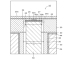
- FIG. 2 is a partially enlarged view of FIG. 5 is an explanatory diagram of a process of joining the power supply member 50 to the electrostatic electrode 22.
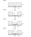
- FIG. 5 is an explanatory diagram of a process of joining the power supply member 50 to the electrostatic electrode 22.
- FIG. 1 is a cross-sectional view showing the schematic configuration of the wafer mounting table 10 of this embodiment (a cross-sectional view when the wafer mounting table 10 is cut along a plane including the central axis of the wafer mounting table 10), and FIG. 2 is an enlarged view of a portion of FIG. 1 (an enlarged view of the area within the frame indicated by the two-dot chain line).
- FIG. 1 is a cross-sectional view showing the schematic configuration of the wafer mounting table 10 of this embodiment (a cross-sectional view when the wafer mounting table 10 is cut along a plane including the central axis of the wafer mounting table 10)
- FIG. 2 is an enlarged view of a portion of FIG. 1 (an enlarged view of the area within the frame indicated by the two-dot chain line).
- the terms up/down, left/right, and front/rear may be used, but these terms merely refer to relative positional relationships.
- the wafer mounting table 10 is an example of a semiconductor manufacturing equipment component used to process a wafer W. As shown in FIG. 1, the wafer mounting table 10 includes a ceramic plate 20, a cooling plate 30, a bonding layer 40, and a power supply member 50.
- the ceramic plate 20 is a disk-shaped member having a wafer mounting surface 20a on its upper surface.
- the ceramic plate 20 is formed from a ceramic-containing material.
- a ceramic-containing material is a material whose main component is ceramic, and may contain, in addition to ceramic, components derived from sintering aids (such as rare earth elements) and unavoidable components.
- a main component means that it accounts for 50 mass% or more of the total. Examples of ceramics include alumina and aluminum nitride.
- the electrostatic electrode 22 is embedded in the ceramic plate 20.
- the electrostatic electrode 22 is formed of a material containing a metal such as W, Mo, WC, or MoC.
- the metal used for the electrostatic electrode 22 is preferably one whose thermal expansion coefficient is close to that of the ceramic plate 20. To bring the thermal expansion coefficient of the electrostatic electrode 22 close to that of the ceramic plate 20, the electrostatic electrode 22 may contain the ceramic contained in the ceramic plate 20.
- the electrostatic electrode 22 is a disk-shaped or mesh-shaped monopolar electrostatic electrode.
- the layer of the ceramic plate 20 above the electrostatic electrode 22 functions as a dielectric layer.
- a DC power source 62 for electrostatic adsorption is connected to the electrostatic electrode 22 via a power supply member 50.
- the cooling plate 30 is a disk-shaped member having a refrigerant flow path 32 inside which a refrigerant can circulate.
- the refrigerant flow path 32 is formed in a single stroke from one end to the other so that it spreads over the entire surface of the ceramic plate 20 in a plan view.
- One end and the other end of the refrigerant flow path 32 are connected to a refrigerant circulation pump (not shown) that has the function of adjusting the temperature of the refrigerant.
- the cooling plate 30 is made of a conductive material containing, for example, a metal. Examples of the conductive material include composite materials and metals.
- composite materials include metal composite materials (also called metal matrix composites (MMCs)), and examples of MMCs include materials containing Si, SiC, and Ti, and materials in which a SiC porous body is impregnated with Al and/or Si.
- MMCs metal matrix composites
- a material containing Si, SiC, and Ti is called SiSiCTi
- AlSiC a material in which a SiC porous body is impregnated with Al
- SiSiC a material in which a SiC porous body is impregnated with Si
- metals include Al, Ti, Mo, and alloys thereof. It is preferable that the conductive material used for the cooling plate 30 has a thermal expansion coefficient close to that of the ceramic plate 20.
- the bonding layer 40 bonds the lower surface of the ceramic plate 20 to the upper surface of the cooling plate 30.
- the bonding layer 40 may be, for example, a metal bonding layer formed of solder or a metal brazing material.
- the metal bonding layer may be formed, for example, by TCB (thermal compression bonding).
- TCB refers to a known method in which a metal bonding material is sandwiched between two members to be bonded, and the two members are pressure-bonded while being heated to a temperature below the solidus temperature of the metal bonding material.
- An organic adhesive layer may be used as the bonding layer 40 instead of the metal bonding layer.
- the power supply member 50 is a metal member that supplies power to the electrostatic electrode 22.
- the power supply member 50 is, for example, a metal rod.
- Metals used for the power supply member 50 include, for example, W, Mo, Ni, etc., and it is preferable that the thermal expansion coefficient of the metal is close to that of the ceramic plate 20.
- the power supply member 50 is inserted from the underside of the cooling plate 30 through the cooling plate through hole 34 that passes through the cooling plate 30 in the vertical direction and the bonding layer through hole 44 that passes through the bonding layer 40 in the vertical direction, into the power supply member insertion hole 24 provided in the ceramic plate 20.
- the diameter of the bonding layer through hole 44 is the same as the diameter of the cooling plate through hole 34.
- the power supply member 50 is electrically connected to the electrostatic electrode 22.
- the joining structure between the power supply member 50 and the electrostatic electrode 22 will be described with reference to FIG. 2.
- the power supply member 50 passes through the inside of the insulating tube 36 arranged in the cooling plate through hole 34 and is inserted into the power supply member insertion hole 24 with some play.
- the outer circumferential surface of the insulating tube 36 is bonded to the inner circumferential surface of the cooling plate through hole 34 via an adhesive layer 35.
- the upper end surface of the insulating tube 36 is higher than the upper surface of the cooling plate 30 and is located below the lower surface of the ceramic plate 20.
- the power supply member insertion hole 24 is a cylindrical hole and is provided so as to reach from the lower surface of the ceramic plate 20 to just before the electrostatic electrode 22.
- the boundary portion 24a (the portion surrounded by a dashed line frame in FIG. 2) between the bottom surface and the side surface of the power supply member insertion hole 24 is chamfered.
- the chamfering may be R chamfering or C chamfering.
- a recessed hole 25 is provided in the bottom surface of the power supply member insertion hole 24.
- the recessed hole 25 is provided so as to reach the electrode extraction portion 22a added to the electrostatic electrode 22.
- the diameter D1 of the opening of the recessed hole 25 is smaller than the diameter D2 of the power supply member insertion hole 24 and is equal to or larger than the diameter D3 of the power supply member 50.
- the opening of the recessed hole 25 does not reach the chamfered boundary portion 24a of the power supply member insertion hole 24.
- the power supply member 50 is electrically connected to the electrode extraction portion 22a provided on the electrostatic electrode 22 via a first solder layer 26 and a second solder layer 27.
- the electrode extraction portion 22a is a circular plate member made of the same material as the electrostatic electrode 22. The lower surface of the electrode extraction portion 22a is exposed to the bottom surface of the recessed hole 25.
- the first brazing material layer 26 fills the recessed hole 25.
- the first brazing material layer 26 is a layer formed by a first brazing material containing an active metal.
- the surface (lower surface) of the first brazing material layer 26 is flush with the bottom surface of the power supply member insertion hole 24.
- the first brazing material include silver brazing, copper brazing, nickel brazing, gold brazing, and palladium brazing containing active metals.
- active metals include titanium, zirconium, hafnium, vanadium, niobium, and beryllium.
- Specific examples of the first brazing material include Ag-Cu-Ti brazing material and Ag-Cu-Ti-Sn brazing material.
- first brazing materials are processed at 700°C or higher, so there is a possibility that a chemical reaction occurs at the interface between the ceramic plate 20 and the first brazing material to form a reaction layer, and it is believed that such a reaction layer plays a role in increasing the bonding strength between the ceramic plate 20 and the first brazing material layer 26.
- the second brazing material layer 27 joins the entire tip surface 50a of the power supply member 50 to the first brazing material layer 26.
- the second brazing material layer 27 is provided so as not to reach the boundary portion 24a of the power supply member insertion hole 24.
- the second brazing material layer 27 is a layer formed of a second brazing material that does not contain active metals. Examples of the second brazing material include Au-Ge brazing material, Au-Sn brazing material, and Au-Si brazing material.
- the first brazing material basically wets and spreads on the surface of the first brazing material layer 26, but does not wet and spread easily on the surface of the ceramic plate 20. Therefore, the second brazing material layer 27 is formed without protruding significantly from the surface of the first brazing material layer 26.
- the melting point of the second brazing material is lower than that of the first brazing material (for example, 200 to 500°C), so the processing temperature of the second brazing material is lower than that of the first brazing material.
- the wafer mounting table 10 is installed in a vacuum chamber (not shown), and the wafer W is mounted on the wafer mounting surface 20a of the wafer mounting table 10. Then, a voltage is applied to the electrostatic electrode 22 from the DC power source 62 via the power supply member 50. Then, the wafer W is attracted and fixed to the wafer mounting surface 20a. Then, the inside of the vacuum chamber is set to a vacuum atmosphere or a reduced pressure atmosphere, and the wafer W is processed in the vacuum chamber.
- an upper electrode equipped with a shower head is placed on the ceiling of the vacuum chamber, and a high frequency voltage is applied between the upper electrode and the cooling plate 30 while a reactive gas is supplied from the shower head to the space between the wafer W and the upper electrode to generate plasma.
- the application of the voltage to the electrostatic electrode 22 is released.
- the wafer W is released from the attraction and fixation to the wafer mounting surface 20a.
- a coolant is passed through the coolant flow passage 32 when it is necessary to lower the temperature of the wafer W.
- FIG. 3 is an explanatory diagram of this process.
- a ceramic plate 20 is prepared in which an electrostatic electrode 22 and an electrode extraction portion 22a that contacts the electrostatic electrode 22 are embedded (FIG. 3A).
- Such a ceramic plate 20 can be prepared by a known method.
- the surface of the ceramic plate 20 that will become the wafer mounting surface 20a faces downward.
- a cylindrical first hole 125 is formed from one surface of the ceramic plate 20 toward the electrode lead-out portion 22a ( Figure 3B). At this time, the first hole 125 is formed so that the electrode lead-out portion 22a is exposed at the bottom surface of the first hole 125.
- the first hole 125 can be formed, for example, by countersinking.
- the diameter of the first hole 125 is the same as the diameter of the opening of the recessed hole 25.
- the boundary between the bottom surface and the side surface of the first hole 125 is made to have a chamfered shape.
- a first solder layer 126 is formed over the entire bottom surface of the first hole 125 (FIG. 3C).
- the first solder layer 126 can be formed, for example, by cutting a sheet of a first solder containing an active metal to fit the size of the bottom surface of the first hole 125, heating and melting the first solder while the sheet is laid on the bottom surface of the first hole 125, and then cooling and solidifying it.
- the first solder layer 26 may be formed by a gas phase method (CVD, sputtering) or a liquid phase method (electrolytic plating, electroless plating).
- a cylindrical second hole, the power supply member insertion hole 24, is formed from the surface of the ceramic plate 20 where the first hole 125 is formed toward the first solder layer 126 so as to be coaxial with the first hole 125 (FIG. 3D).
- the power supply member insertion hole 24 can be formed, for example, by countersinking.
- the power supply member insertion hole 24 is formed so that the bottom surface of the power supply member insertion hole 24 is above the bottom surface of the first hole 125 and below the surface of the first solder layer 126.
- the boundary 24a between the bottom surface and the side surface of the power supply member insertion hole 24 has a chamfered shape.
- the surface of the first solder layer 126 is scraped off to become the first solder layer 26 (FIG. 3D), and the surface of the first solder layer 26 becomes flush with the bottom surface of the power supply member insertion hole 24.
- a sheet of a second solder material that does not contain active metal (or has a lower content of active metal than the first solder material) is placed on the first solder material layer 26, and the power supply member 50 is placed on the second solder material.
- the sheet of the second solder material is sandwiched between the first solder material layer 26 and the tip surface 50a of the power supply member 50.
- the melting point of the second solder material is lower than that of the first solder material.
- the size of the sheet of the second solder material is adjusted so that it is equivalent to the size of the first solder material layer 26 when the sheet of the second solder material melts and then solidifies.
- the sheet is treated at a temperature equal to or higher than the melting point of the second solder material and lower than the melting point of the first solder material. Then, the second solder material melts. The second solder material easily spreads on the surface of the first solder material layer 26, but does not easily spread on the outer region (ceramic plate 20) of the first solder material layer 26. Therefore, after the second brazing material has solidified, the second brazing material layer 27 remains mostly in the area where the first brazing material layer 26 was formed. As a result, the diameter of the second brazing material layer 27 is equal to or larger than the diameter D2 of the power supply member 50 and does not reach the chamfered boundary portion 24a of the power supply member insertion hole 24.
- the interface between the first brazing material layer 26 and the second brazing material layer 27 becomes a region where the components of both layers 26, 27 diffuse.
- the interface between the first brazing material layer 26 and the second brazing material layer 27 is clearly shown in Figure 2, in reality, this interface becomes a region where the components of both layers 26, 27 diffuse (a gradation region).
- the process of joining the power supply member 50 to the first solder layer 26 may be performed before joining the cooling plate 30 to the ceramic plate 20, or after joining the cooling plate 30 to the ceramic plate 20.
- the diameter D1 of the opening of the recessed hole 25 is smaller than the diameter D2 of the power supply member insertion hole 24 and is equal to or larger than the diameter D3 of the power supply member 50.
- the first solder layer 26 is filled in the recessed hole 25. Therefore, the first solder layer 26 does not exist or is almost not present outside the opening of the recessed hole 25.
- the second solder layer 27 joins the entire tip surface 50a of the power supply member 50 to the first solder layer 26. This second solder layer 27 is provided so as not to reach the boundary portion 24a of the power supply member insertion hole 24.
- the second solder layer 27 reaches the boundary portion 24a, the second solder will easily creep up from the boundary portion 24a to the side of the power supply member insertion hole 24 and the side of the power supply member 50 during manufacturing, and voids (pores) will easily occur in the second solder layer 27 between the power supply member 50 and the first solder layer 26.
- the second brazing material layer 27 does not reach the boundary portion 24a, the second brazing material is prevented from creeping up the side of the power supply member insertion hole 24 or the side of the power supply member 50 during manufacturing, and the occurrence of a gap in the second brazing material layer 27 between the power supply member 50 and the first brazing material layer 26 can be prevented. Therefore, power can be supplied to the electrostatic electrode 22 by the power supply member 50 in a good manner.
- the boundary 24a is chamfered. This makes it possible to prevent cracks from occurring starting from the boundary 24a of the power supply member insertion hole 24.
- the second solder layer 27 does not reach the chamfered boundary 24a. This makes it possible to further prevent the second solder from creeping up onto the side of the power supply member insertion hole 24 or the side of the power supply member 50 during manufacturing.
- the edge 50b of the tip surface 50a of the power supply member 50 is chamfered, it is preferable that the chamfering be performed to C 0.3 or less or R 0.3 or less. In this way, the area of the tip surface 50a of the power supply member 50 is increased, and therefore the contact area between the tip surface 50a of the power supply member 50 and the second brazing material layer 27 is increased.
- the first brazing material layer 26 contains an active metal
- the second brazing material layer 27 does not contain an active metal or has a lower content of active metal than the first brazing material layer 26.
- the first brazing material layer 26 contains an active metal and therefore tends to wet and spread over the surface of the recessed hole 25 (ceramic plate 20).
- the second brazing material layer 27 does not contain an active metal or has a low content of active metal, so it does not wet and spread over the surface of the ceramic plate 20 and is unlikely to reach the boundary 24a of the power supply member insertion hole 24.
- the interface between the first brazing layer 26 and the second brazing layer 27 may be a region where the components contained in the first brazing layer 26 and the components contained in the second brazing layer 27 are diffused.
- the second brazing layer 27, which does not contain active metal or has a low content of active metal, is formed on the first brazing layer 26, which contains active metal, but at the interface between the first brazing layer 26 and the second brazing layer 27, the components contained in both layers tend to diffuse, resulting in a region where both components are mixed together.
- the distance (insulation distance) between the second solder layer 27 and the cooling plate 30 can be made longer than when the second solder layer 27 is provided along the side of the power supply member insertion hole 24, and insulation breakdown can be avoided.
- the first brazing material layer 26 and the second brazing material layer 27 do not have a stress relaxation member therein (for example, a member formed of a material whose thermal expansion coefficient is lower than that of the power supply member 50 and higher than that of the ceramic plate 20), but this is not particularly limited.
- the first brazing material layer 26 may have a stress relaxation member therein.
- the second brazing material layer 27 may have a stress relaxation member therein, but it is preferable that it does not have one.
- a metal rod is used as the power supply member 50, but this is not particularly limited and may be, for example, a metal cable.
- the wafer mounting table 10 may have at least one of a heater electrode and an RF electrode (electrode for generating plasma) embedded in the ceramic plate 20 instead of or in addition to the electrostatic electrode 22.
- the joint structure between the heater electrode and the power supply member for the heater electrode and the joint structure between the RF electrode and the power supply member for the RF electrode may be the same as the joint structure between the electrostatic electrode 22 and the power supply member 50 described above.
- the electrode extraction portion 22a is added to the electrostatic electrode 22, but it is also possible to expose a portion of the electrostatic electrode 22 directly to the bottom surface of the recessed hole 25 without providing the electrode extraction portion 22a.
- the power supply member 50 is made of a material that is difficult to wet and spread with the second solder
- a metal coating that is easy for the second solder to spread may be formed on the tip surface 50a of the power supply member 50.
- the power supply member 50 is made of Mo
- a Ni coating may be formed on the tip surface 50a.
- the metal coating may be formed on the chamfered portion of the tip surface 50a and its edge 50b of the power supply member 50, and may be further provided to a height of 0.1 mm or less from the chamfered portion. This level of height can prevent the occurrence of gaps in the second solder layer 27 between the power supply member 50 and the first solder layer 26.
- the present invention can be used in semiconductor manufacturing equipment used to process wafers.
Landscapes
- Physics & Mathematics (AREA)
- Engineering & Computer Science (AREA)
- Plasma & Fusion (AREA)
- Chemical & Material Sciences (AREA)
- Analytical Chemistry (AREA)
- Container, Conveyance, Adherence, Positioning, Of Wafer (AREA)
- Jigs For Machine Tools (AREA)
Abstract
ウエハ載置台10は、静電電極22が埋設されたセラミックプレート20と、セラミックプレート20の下面から静電電極22の手前に達するように設けられた給電部材挿入穴24と、給電部材挿入穴24にあそびをもって挿入された金属製の給電部材50と、給電部材挿入穴24の底面から静電電極22(電極取出部22a)に達するように設けられた凹穴25と、凹穴25に充填された第1ロウ材層26と、給電部材50の先端面50aの全体と第1ロウ材層26とを接合する第2ロウ材層27とを備える。凹穴25の開口部の直径D1は、給電部材挿入穴24の直径D2よりも小さく且つ給電部材50の直径D3と同等かそれより大きい。第2ロウ材層27は、給電部材挿入穴24の底面と側面との境界部24aに達しないように設けられている。
Description
本発明は、半導体製造装置用部材に関する。
半導体製造装置においては、ウエハを加熱するためのセラミックヒータやウエハを吸着保持するための静電チャックなどの半導体製造装置用部材が採用されている。特許文献1には、この種の半導体製造装置用部材において、セラミックプレートに埋設された電極に給電部材を接合する構造が開示されている。具体的には、セラミックプレートの下面から電極の手前に達するように給電部材挿入穴が設けられ、給電部材挿入穴の底面から電極に付加された電極取出部に達するように凹状の収容部が設けられている。収容部には、第1の金属円板が収容されている。第1の金属円板は、電極取出部に第1のロウ材層によって接合されている。給電部材は、給電部材挿入穴にあそびをもって挿入されている。給電部材の先端面と第1の金属円板との間には、第2の金属円板を内包する第2のロウ材層が設けられている。第2のロウ材層は、給電部材挿入穴の底面全体を覆うように(すなわち給電部材挿入穴の底面と側面との境界部に達するように)設けられている。また、第2のロウ材層は、給電部材の先端面の全体に接するように且つ給電部材の側面に這い上がるように設けられている(特許文献1の図3)。あるいは、第2のロウ材層は、給電部材の先端面の中央部には接するが外周部には接しないように設けられている(特許文献1の図4及び図5)。
しかしながら、特許文献1では、第2のロウ材層が給電部材挿入穴の底面全体を覆うように(すなわち給電部材挿入穴の底面と側面との境界部に達するように)設けられているため、第2のロウ材層が給電部材の先端面全体と接するように設計すると、製造時に第2のロウ材が給電部材の側面を這い上がりやすい。その場合、給電部材の先端面と第2の金属円板との間や第2の金属円板と第1の金属円板との間の第2のロウ材が不足してその部分に空隙(気孔)が生じることがあった。こうした空隙は、給電不良等の不具合の原因となる。一方、第2のロウ材層が給電部材の先端面の中央部のみと接するように設計すると、両者の接触面積を十分確保することができず、給電不良等の不具合が発生するおそれがあった。
本発明は、上述した課題を解決するためになされたものであり、セラミックプレートに埋設された電極への給電部材による給電を良好に行うことを主目的とする。
[1]本発明の半導体製造装置用部材は、
上面にウエハ載置面を有し、電極が埋設されたセラミックプレートと、
前記セラミックプレートの下面から前記電極の手前に達するように設けられた給電部材挿入穴と、
前記給電部材挿入穴にあそびをもって挿入された給電部材と、
前記給電部材挿入穴の底面から前記電極又は前記電極に付加された電極取出部に達するように設けられ、開口部の直径が前記給電部材挿入穴の直径よりも小さく且つ前記給電部材の直径と同等かそれより大きい凹穴と、
前記凹穴に充填された第1ロウ材層と、
前記給電部材の端面全体と前記第1ロウ材層とを接合し、前記給電部材挿入穴の底面と側面との境界部に達しないように設けられた第2ロウ材層と、
を備えたものである。
上面にウエハ載置面を有し、電極が埋設されたセラミックプレートと、
前記セラミックプレートの下面から前記電極の手前に達するように設けられた給電部材挿入穴と、
前記給電部材挿入穴にあそびをもって挿入された給電部材と、
前記給電部材挿入穴の底面から前記電極又は前記電極に付加された電極取出部に達するように設けられ、開口部の直径が前記給電部材挿入穴の直径よりも小さく且つ前記給電部材の直径と同等かそれより大きい凹穴と、
前記凹穴に充填された第1ロウ材層と、
前記給電部材の端面全体と前記第1ロウ材層とを接合し、前記給電部材挿入穴の底面と側面との境界部に達しないように設けられた第2ロウ材層と、
を備えたものである。
この半導体製造装置用部材では、凹穴の開口部の直径は、給電部材挿入穴の直径よりも小さく且つ給電部材の直径と同等かそれより大きい。第1ロウ材層は、凹穴に充填されている。第2ロウ材層は、給電部材の端面全体と第1ロウ材層とを接合している。この第2ロウ材層は、給電部材挿入穴の底面と側面との境界部に達しないように設けられている。第2ロウ材層が境界部に達していると、製造時に第2ロウ材が境界部から給電部材挿入穴の側面や給電部材の側面に這い上がりやすくなり、給電部材と第1ロウ材層との間の第2ロウ材層に空隙(気孔)が生じやすくなる。しかし、ここでは第2ロウ材層が境界部に達していないため、製造時に第2ロウ材が給電部材挿入穴の側面や給電部材の側面に這い上がるのを抑制でき、給電部材と第1ロウ材層との間の第2ロウ材層に空隙が生じるのを防止できる。したがって、セラミックプレートに埋設された電極への給電部材による給電を良好に行うことができる。
なお、「境界部」とは、給電部材挿入穴の底面と側面とが交叉している部分である。「境界部」が面取りされていない場合、「境界部」は給電部材挿入穴の底面と側面とが交叉しているエッジである。そのエッジが面取りされている場合、「境界部」はエッジが面取りされたあとの部分(例えばC面取りであればC面全体、R面取りであればR面全体)である。
[2]本発明の半導体製造装置用部材(前記[1]に記載の半導体製造装置用部材)において、前記境界部は、面取りされていてもよく、前記第2ロウ材層は、面取りされた前記境界部に至らないように設けられていてもよい。こうすれば、給電部材挿入穴の境界部を起点としてクラックが発生するのを防止することができる。また、第2ロウ材層は、面取りされた境界部に至っていないため、製造時に第2ロウ材が給電部材挿入穴の側面や給電部材の側面に這い上がるのをより抑制することができる。
[3]本発明の半導体製造装置用部材(前記[1]又は[2]に記載の半導体製造装置用部材)において、前記給電部材の端面のエッジは、C0.3以下又はR0.3以下に面取りされていてもよい。こうすれば、給電部材の端面の面積が広くなるため、給電部材の端面と第2ロウ材層との接触面積が広くなる。
[4]本発明の半導体製造装置用部材(前記[1]~[3]のいずれかに記載の半導体製造装置用部材)において、前記第1ロウ材層は、活性金属を含有していてもよく、前記第2ロウ材層は、活性金属を含有しないか活性金属の含有量が前記第1ロウ材層よりも低くてもよい。この場合、第1ロウ材層を形成する際、第1ロウ材は活性金属を含有しているため凹穴(セラミックプレート)の表面に濡れ広がりやすい。一方、第2ロウ材層を形成する際、第2ロウ材は活性金属を含有していないか含有量が少ないため、セラミックプレートの表面に濡れ広がりにくく、給電部材挿入穴の境界部に達しにくい。
[5]本発明の半導体製造装置用部材(前記[4]に記載の半導体製造装置用部材)において、前記第1ロウ材層と前記第2ロウ材層との界面は、前記第1ロウ材層に含まれる成分と前記第2ロウ材層に含まれる成分とが拡散した領域となっていてもよい。製造時、活性金属を含有する第1ロウ材層に活性金属を含有しないかその含有量が少ない第2ロウ材層を形成するが、第1ロウ材層と第2ロウ材層との界面では両層に含まれる成分が拡散して両成分が入り交じった領域になりやすい。
[6]本発明の半導体製造装置用部材(前記[1]~[5]のいずれかに記載の半導体製造装置用部材)は、前記セラミックプレートの下面に設けられた導電性の冷却プレートと、前記冷却プレートを上下方向に貫通して前記給電部材挿入穴に連通し、前記給電部材が挿通される冷却プレート貫通穴と、を備えていてもよい。この場合、第2ロウ材層は給電部材挿入穴の底面と側面との境界部に達していないため、第2ロウ材層が給電部材挿入穴の側面に沿って設けられている場合に比べて、第2ロウ材層と冷却プレートとの距離(絶縁距離)を長くすることができる。
図1は本実施形態のウエハ載置台10の概略構成を示す断面図(ウエハ載置台10の中心軸を含む面でウエハ載置台10を切断したときの断面図)、図2は図1の部分拡大図(2点鎖線で示した枠内の拡大図)である。なお、以下の説明において、上下、左右、前後を用いることがあるが、上下、左右、前後は、相対的な位置関係に過ぎない。
ウエハ載置台10は、ウエハWを処理するために用いられる半導体製造装置用部材の一例である。ウエハ載置台10は、図1に示すように、セラミックプレート20と、冷却プレート30と、接合層40と、給電部材50とを備える。
セラミックプレート20は、上面にウエハ載置面20aを有する円板状の部材である。セラミックプレート20は、セラミック含有材料で形成されている。セラミック含有材料は、セラミックを主成分とする材料であり、セラミックの他に焼結助剤に由来する成分(例えば希土類元素等)や不可避成分などを含んでいてもよい。主成分とは、全体に占める割合が50質量%以上であることをいう。セラミックとしては、例えばアルミナや窒化アルミニウムなどが挙げられる。
セラミックプレート20には、静電電極22が埋設されている。静電電極22は、例えばW、Mo、WC、MoCなどの金属を含有する材料によって形成されている。静電電極22に用いる金属としては、熱膨張係数がセラミックプレート20の熱膨張係数に近いものが好ましい。静電電極22の熱膨張係数をセラミックプレート20の熱膨張係数に近づけるために、セラミックプレート20に含まれるセラミックを静電電極22に含有させてもよい。静電電極22は、円板状又はメッシュ状の単極型の静電電極である。セラミックプレート20のうち静電電極22よりも上側の層は誘電体層として機能する。静電電極22には、静電吸着用の直流電源62が給電部材50を介して接続されている。
冷却プレート30は、内部に冷媒が循環可能な冷媒流路32を備えた円板状の部材である。冷媒流路32は、平面視でセラミックプレート20の全面に行き渡るように、一端から他端まで一筆書きの要領で形成されている。冷媒流路32の一端と他端は、冷媒の温度を調節する機能を有する冷媒循環ポンプ(図示せず)に接続されている。冷却プレート30は、例えば金属を含有する導電材料で作製されている。導電材料としては、例えば、複合材料や金属などが挙げられる。複合材料としては、金属複合材料(メタル・マトリックス・コンポジット(MMC)ともいう)などが挙げられ、MMCとしては、Si,SiC及びTiを含む材料やSiC多孔質体にAl及び/又はSiを含浸させた材料などが挙げられる。Si,SiC及びTiを含む材料をSiSiCTiといい、SiC多孔質体にAlを含浸させた材料をAlSiCといい、SiC多孔質体にSiを含浸させた材料をSiSiCという。金属としては、Al,Ti,Mo又はそれらの合金などが挙げられる。冷却プレート30に用いる導電材料としては、熱膨張係数がセラミックプレート20の熱膨張係数に近いものが好ましい。
接合層40は、セラミックプレート20の下面と冷却プレート30の上面とを接合している。接合層40は、例えば、はんだや金属ロウ材で形成された金属接合層であってもよい。金属接合層は、例えばTCB(Thermal compression bonding)により形成されていてもよい。TCBとは、接合対象の2つの部材の間に金属接合材を挟み込み、金属接合材の固相線温度以下の温度に加熱した状態で2つの部材を加圧接合する公知の方法をいう。接合層40として、金属接合層の代わりに有機接着層を採用してもよい。
給電部材50は、静電電極22に電力を供給する金属製の部材である。給電部材50は、例えば金属ロッドである。給電部材50に用いられる金属は、例えばW,Mo,Niなどであり、その金属の熱膨張係数がセラミックプレート20の熱膨張係数に近いものが好ましい。給電部材50は、冷却プレート30の下面側から、冷却プレート30を上下方向に貫通する冷却プレート貫通穴34及び接合層40を上下方向に貫通する接合層貫通穴44を経て、セラミックプレート20に設けられた給電部材挿入穴24に挿入されている。接合層貫通穴44の直径は、冷却プレート貫通穴34の直径と同じである。給電部材50は、静電電極22と電気的に接続されている。
給電部材50と静電電極22との接合構造について、図2を用いて説明する。給電部材50は、冷却プレート貫通穴34に配置された絶縁管36の内部を通過して、給電部材挿入穴24にあそびをもって挿入されている。絶縁管36の外周面は、冷却プレート貫通穴34の内周面に接着層35を介して接着されている。絶縁管36の上端面は、冷却プレート30の上面よりも高くセラミックプレート20の下面以下に位置している。給電部材挿入穴24は、円柱状の穴であり、セラミックプレート20の下面から静電電極22の手前に達するように設けられている。給電部材挿入穴24の底面と側面との境界部24a(図2の1点鎖線の枠で囲んだ部分)は、面取りされている。面取りは、R面取りであってもよいしC面取りであってもよい。給電部材挿入穴24の底面には、凹穴25が設けられている。凹穴25は、静電電極22に付加された電極取出部22aに達するように設けられている。凹穴25の開口部の直径D1は、給電部材挿入穴24の直径D2よりも小さく且つ給電部材50の直径D3と同等かそれより大きい。凹穴25の開口部は、給電部材挿入穴24の面取りされた境界部24aに達していない。
給電部材50は、静電電極22に設けられた電極取出部22aに、第1ロウ材層26及び第2ロウ材層27を介して電気的に接続されている。電極取出部22aは、静電電極22と同じ材料で形成された円板部材である。電極取出部22aの下面は、凹穴25の底面に露出している。
第1ロウ材層26は、凹穴25に充填されている。第1ロウ材層26は、活性金属を含有する第1ロウ材によって形成された層である。第1ロウ材層26の表面(下面)は、給電部材挿入穴24の底面と同一平面になっている。第1ロウ材としては、例えば、銀ロウや銅ロウ、ニッケルロウ、金ロウ、パラジウムロウなどに活性金属を含有させたものが挙げられる。活性金属としては、例えば、チタン、ジルコニウム、ハフニウム、バナジウム、ニオブ、ベリリウムなどが挙げられる。第1ロウ材の具体例としては、Ag-Cu-Tiロウ材、Ag-Cu-Ti-Snロウ材などが挙げられる。これらの第1ロウ材は700℃以上で処理されるため、セラミックプレート20と第1ロウ材との界面で化学反応が起こって反応層が形成される可能性があり、こうした反応層はセラミックプレート20と第1ロウ材層26との接合強度を高める役割を果たすと考えられる。
第2ロウ材層27は、給電部材50の先端面50aの全体と第1ロウ材層26とを接合する。第2ロウ材層27は、給電部材挿入穴24の境界部24aに達しないように設けられている。第2ロウ材層27は、活性金属を含有しない第2ロウ材によって形成された層である。第2ロウ材としては、例えば、Au-Geロウ材、Au-Snロウ材、Au-Siロウ材などが挙げられる。第1ロウ材は、基本的には第1ロウ材層26の表面に濡れ広がるが、セラミックプレート20の表面には濡れ広がりにくい。そのため、第2ロウ材層27は、第1ロウ材層26の表面から大きくはみ出すことなく形成される。第2ロウ材の融点は第1ロウ材の融点よりも低い(例えば200~500℃)ため、第2ロウ材の処理温度は第1ロウ材の処理温度よりも低い。
給電部材50の先端面50aの面積が広いほど第2ロウ材層27との接合面積が広くなるため、先端面50aのエッジ50bは面取りされていなくてもよく、面取りされているとしてもC0.3以下にC面取りされるかR0.3以下にR面取りされていることが好ましい。
次に、ウエハ載置台10の使用例について説明する。まず、図示しない真空チャンバ内にウエハ載置台10を設置し、そのウエハ載置台10のウエハ載置面20aにウエハWを載置する。そして、直流電源62から給電部材50を介して静電電極22に電圧を印加する。すると、ウエハWがウエハ載置面20aに吸着固定される。そして、真空チャンバ内を真空雰囲気もしくは減圧雰囲気になるように設定し、真空チャンバ内でウエハWに処理を施す。例えば、ウエハWをプラズマで処理する際には、真空チャンバ内の天井にシャワーヘッドを備えた上部電極を配置し、ウエハWと上部電極との間の空間にシャワーヘッドから反応ガスを供給しながら上部電極と冷却プレート30との間に高周波電圧を印加してプラズマを発生させる。ウエハWの処理が終了した後、静電電極22への電圧の印加を解除する。すると、ウエハWのウエハ載置面20aへの吸着固定が解除される。なお、冷媒流路32には、ウエハWの温度を下げる必要があるときに冷媒を流す。
次に、ウエハ載置台10の製造方法のうち、特に給電部材50を静電電極22に接合する工程について、図3を用いて説明する。図3はこの工程の説明図である。
まず、静電電極22及び静電電極22と接触する電極取出部22aを埋設したセラミックプレート20を作製する(図3A)。こうしたセラミックプレート20は、公知の方法によって作製することができる。なお、図3A~図3Dでは、セラミックプレート20のウエハ載置面20aになる表面が下向きになるようにした。
続いて、セラミックプレート20の一方の表面から電極取出部22aに向かって円柱状の第1穴125を形成する(図3B)。このとき、第1穴125の底面に電極取出部22aが露出するように第1穴125を形成する。第1穴125は、例えば座繰り加工によって形成することができる。第1穴125の直径は、凹穴25の開口部の直径と同じである。第1穴125の底面と側面との境界部は、面取りされた形状になるようにする。
続いて、第1穴125の底面の全面に第1ロウ材層126を形成する(図3C)。第1ロウ材層126は、例えば、活性金属を含む第1ロウ材のシートを第1穴125の底面の大きさに合わせて切断し、そのシートを第1穴125の底面に敷設した状態で第1ロウ材を加熱溶融させ、その後冷却して固化することにより、形成することができる。あるいは、第1ロウ材層26を、気相法(CVD、スパッタ)や液相法(電解めっき、無電解めっき)により形成してもよい。
続いて、セラミックプレート20の第1穴125を形成した面から第1ロウ材層126に向かって、円柱状の第2穴である給電部材挿入穴24を第1穴125と同軸になるように形成する(図3D)。給電部材挿入穴24は、例えば座繰り加工によって形成することができる。給電部材挿入穴24は、給電部材挿入穴24の底面が第1穴125の底面よりも上方で且つ第1ロウ材層126の表面よりも下方になるように形成される。給電部材挿入穴24の底面と側面との境界部24aは、面取りされた形状になる。給電部材挿入穴24が形成されると、第1ロウ材層126は表層が削り取られて第1ロウ材層26になり(図3D)、第1ロウ材層26の表面は給電部材挿入穴24の底面と同一平面になる。
続いて、第1ロウ材層26の上に活性金属を含まない(あるいは活性金属の含有量が第1ロウ材よりも低い)第2ロウ材のシートを配置し、第2ロウ材の上に給電部材50を配置する。つまり、第2ロウ材のシートを第1ロウ材層26と給電部材50の先端面50aとで挟み込む。第2ロウ材の融点は第1ロウ材の融点よりも低い。第2ロウ材のシートの大きさは、第2ロウ材のシートが溶融したあと固化したときに第1ロウ材層26の大きさと同等となるように調整する。この状態で、第2ロウ材の融点以上第1ロウ材の融点未満の温度で処理する。すると、第2ロウ材が溶融する。第2ロウ材は、第1ロウ材層26の表面に濡れ広がりやすいが、第1ロウ材層26の外側の領域(セラミックプレート20)には濡れ広がりにくい。そのため、第2ロウ材が固化した後の第2ロウ材層27は、第1ロウ材層26が形成された領域に概ねとどまる。その結果、第2ロウ材層27の直径は、給電部材50の直径D2と同等かそれより大きく且つ給電部材挿入穴24の面取りされた境界部24aに達しない大きさになる。
第2ロウ材の融点以上第1ロウ材の融点未満の温度で処理したとき、第1ロウ材層26に含まれる成分と第2ロウ材に含まれる成分とが拡散する。そのため、第1ロウ材層26と第2ロウ材層27との界面は、両層26,27の成分が拡散した領域となる。図2には、第1ロウ材層26と第2ロウ材層27との界面を明記したが、実際には、この界面は両層26,27の成分が拡散した領域(グラデーション領域)になる。
給電部材50を第1ロウ材層26に接合する工程は、セラミックプレート20に冷却プレート30を接合する前に行ってもよいし、セラミックプレート20に冷却プレート30を接合した後に行ってもよい。
以上説明したウエハ載置台10では、凹穴25の開口部の直径D1は、給電部材挿入穴24の直径D2よりも小さく且つ給電部材50の直径D3と同等かそれより大きい。第1ロウ材層26は、凹穴25に充填されている。そのため、凹穴25の開口部の外側には第1ロウ材層26が存在しないかほぼ存在しない。第2ロウ材層27は、給電部材50の先端面50aの全体と第1ロウ材層26とを接合している。この第2ロウ材層27は、給電部材挿入穴24の境界部24aに達しないように設けられている。第2ロウ材層27が境界部24aに達していると、製造時に第2ロウ材が境界部24aから給電部材挿入穴24の側面や給電部材50の側面に這い上がりやすくなり、給電部材50と第1ロウ材層26との間の第2ロウ材層27に空隙(気孔)が生じやすくなる。しかし、ここでは第2ロウ材層27が境界部24aに達していないため、製造時に第2ロウ材が給電部材挿入穴24の側面や給電部材50の側面に這い上がるのを抑制でき、給電部材50と第1ロウ材層26との間にある第2ロウ材層27に空隙が生じるのを防止できる。したがって、静電電極22への給電部材50による給電を良好に行うことができる。
また、境界部24aは、面取りされている。そのため、給電部材挿入穴24の境界部24aを起点としてクラックが発生するのを防止することができる。また、第2ロウ材層27は、面取りされた境界部24aに至っていない。そのため、製造時に第2ロウ材が給電部材挿入穴24の側面や給電部材50の側面に這い上がるのをより抑制することができる。
更に、給電部材50の先端面50aのエッジ50bが面取りされている場合、C0.3以下又はR0.3以下に面取りされていることが好ましい。こうすれば、給電部材50の先端面50aの面積が広くなるため、給電部材50の先端面50aと第2ロウ材層27との接触面積が広くなる。
更にまた、第1ロウ材層26は、活性金属を含有し、第2ロウ材層27は、活性金属を含有しないか活性金属の含有量が第1ロウ材層26よりも低い。第1ロウ材層26を形成する際、第1ロウ材は活性金属を含有しているため凹穴25(セラミックプレート20)の表面に濡れ広がりやすい。一方、第2ロウ材層27を形成する際、第2ロウ材は活性金属を含有していないか含有量が少ないため、セラミックプレート20の表面に濡れ広がりにくく、給電部材挿入穴24の境界部24aに達しにくい。
そしてまた、第1ロウ材層26と第2ロウ材層27との界面は、第1ロウ材層26に含まれる成分と第2ロウ材層27に含まれる成分とが拡散した領域となっていてもよい。製造時、活性金属を含有する第1ロウ材層26の上に、活性金属を含有しないかその含有量が少ない第2ロウ材層27を形成するが、第1ロウ材層26と第2ロウ材層27との界面では両層に含まれる成分が拡散して両成分が入り交じった領域になりやすい。
そして更に、第2ロウ材層27は給電部材挿入穴24の境界部24aに達していないため、第2ロウ材層27が給電部材挿入穴24の側面に沿って設けられている場合に比べて、第2ロウ材層27と冷却プレート30との距離(絶縁距離)を長くすることができ、絶縁破壊を回避することができる。
なお、本発明は上述した実施形態に何ら限定されることはなく、本発明の技術的範囲に属する限り種々の態様で実施し得ることはいうまでもない。
上述した実施形態では、第1ロウ材層26及び第2ロウ材層27は内部に応力緩和部材(例えば熱膨張係数が給電部材50の熱膨張係数よりも低く、セラミックプレート20の熱膨張係数よりも高い材料で形成された部材)を有さないものとしたが、特にこれに限定されない。例えば、第1ロウ材層26は、内部に応力緩和部材を有していてもよい。第2ロウ材層27は、内部に応力緩和部材を有していてもよいが、有していない方が好ましい。第2ロウ材層27の内部に応力緩和部材を設けると、第2ロウ材層27のボリュームが大きくなりやすく、第2ロウ材の給電部材50の側面や給電部材挿入穴24の側面への這い上がりを防止しにくくなるからである。
上述した実施形態では、給電部材50として金属ロッドを例示したが、特にこれに限定されるものではなく、例えば金属ケーブルとしてもよい。
上述した実施形態において、ウエハ載置台10は、セラミックプレート20に、静電電極22に代えて又は加えて、ヒータ電極及びRF電極(プラズマ発生用電極)の少なくとも一つを埋設していてもよい。その場合、ヒータ電極とヒータ電極用の給電部材との接合構造やRF電極とRF電極用の給電部材との接合構造は、上述した静電電極22と給電部材50との接合構造と同じにすればよい。
上述した実施形態では、静電電極22に電極取出部22aを付加したが、電極取出部22aを設けることなく、静電電極22の一部が直接、凹穴25の底面に露出するようにしてもよい。
上述した実施形態において、給電部材50が第2ロウ材に濡れ広がりにくい材質で形成されている場合には、給電部材50の先端面50aに第2ロウ材が濡れ広がりやすい金属製の被膜を形成してもよい。例えば、給電部材50がMoの場合には先端面50aにNi製の被膜を形成してもよい。なお、金属製の被膜は、給電部材50の先端面50a及びそのエッジ50bの面取り部に形成してもよいし、更にその面取り部から0.1mm以下の高さまで設けてもよい。この程度の高さであれば、給電部材50と第1ロウ材層26との間の第2ロウ材層27に空隙が生じるのを防止できる。
本発明は、ウエハを処理するために使用する半導体製造装置に用いることができる。
10 ウエハ載置台、20 セラミックプレート、20a ウエハ載置面、22 静電電極、22a 電極取出部、24 給電部材挿入穴、24a 境界部、25 凹穴、26 第1ロウ材層、27 第2ロウ材層、30 冷却プレート、32 冷媒流路、34 冷却プレート貫通穴、35 接着層、36 絶縁管、40 接合層、44 接合層貫通穴、50 給電部材、50a 先端面、50b エッジ、62 直流電源、125 第1穴、126 第1ロウ材層。
Claims (6)
- 上面にウエハ載置面を有し、電極が埋設されたセラミックプレートと、
前記セラミックプレートの下面から前記電極の手前に達するように設けられた給電部材挿入穴と、
前記給電部材挿入穴にあそびをもって挿入された給電部材と、
前記給電部材挿入穴の底面から前記電極又は前記電極に付加された電極取出部に達するように設けられ、開口部の直径が前記給電部材挿入穴の直径よりも小さく且つ前記給電部材の直径と同等かそれより大きい凹穴と、
前記凹穴に充填された第1ロウ材層と、
前記給電部材の端面全体と前記第1ロウ材層とを接合し、前記給電部材挿入穴の底面と側面との境界部に達しないように設けられた第2ロウ材層と、
を備えた半導体製造装置用部材。 - 前記境界部は、面取りされており、
前記第2ロウ材層は、面取りされた前記境界部に至らないように設けられている、
請求項1に記載の半導体製造装置用部材。 - 前記給電部材の端面のエッジは、C0.3以下又はR0.3以下に面取りされている、
請求項1又は2に記載の半導体製造装置用部材。 - 前記第1ロウ材層は、活性金属を含有し、
前記第2ロウ材層は、活性金属を含有しないか活性金属の含有量が前記第1ロウ材層よりも低い、
請求項1又は2に記載の半導体製造装置用部材。 - 前記第1ロウ材層と前記第2ロウ材層との界面は、前記第1ロウ材層に含まれる成分と前記第2ロウ材層に含まれる成分とが拡散した領域となっている、
請求項4に記載の半導体製造装置用部材。 - 請求項1又は2に記載の半導体製造装置用部材であって、
前記セラミックプレートの下面に設けられた導電性の冷却プレートと、
前記冷却プレートを上下方向に貫通して前記給電部材挿入穴に連通し、前記給電部材が挿通される冷却プレート貫通穴と、
を備えた半導体製造装置用部材。
Priority Applications (6)
| Application Number | Priority Date | Filing Date | Title |
|---|---|---|---|
| JP2023569944A JP7606635B1 (ja) | 2023-07-06 | 2023-07-06 | 半導体製造装置用部材 |
| PCT/JP2023/025160 WO2025009162A1 (ja) | 2023-07-06 | 2023-07-06 | 半導体製造装置用部材 |
| CN202380011723.9A CN121444656A (zh) | 2023-07-06 | 2023-07-06 | 半导体制造装置用部件 |
| KR1020237040039A KR102961425B1 (ko) | 2023-07-06 | 반도체 제조 장치용 부재 | |
| US18/510,850 US12622225B2 (en) | 2023-07-06 | 2023-11-16 | Member for semiconductor manufacturing apparatus |
| TW112149448A TW202503951A (zh) | 2023-07-06 | 2023-12-19 | 半導體製造裝置用構件 |
Applications Claiming Priority (1)
| Application Number | Priority Date | Filing Date | Title |
|---|---|---|---|
| PCT/JP2023/025160 WO2025009162A1 (ja) | 2023-07-06 | 2023-07-06 | 半導体製造装置用部材 |
Related Child Applications (1)
| Application Number | Title | Priority Date | Filing Date |
|---|---|---|---|
| US18/510,850 Continuation US12622225B2 (en) | 2023-07-06 | 2023-11-16 | Member for semiconductor manufacturing apparatus |
Publications (1)
| Publication Number | Publication Date |
|---|---|
| WO2025009162A1 true WO2025009162A1 (ja) | 2025-01-09 |
Family
ID=93933908
Family Applications (1)
| Application Number | Title | Priority Date | Filing Date |
|---|---|---|---|
| PCT/JP2023/025160 Ceased WO2025009162A1 (ja) | 2023-07-06 | 2023-07-06 | 半導体製造装置用部材 |
Country Status (5)
| Country | Link |
|---|---|
| US (1) | US12622225B2 (ja) |
| JP (1) | JP7606635B1 (ja) |
| CN (1) | CN121444656A (ja) |
| TW (1) | TW202503951A (ja) |
| WO (1) | WO2025009162A1 (ja) |
Citations (5)
| Publication number | Priority date | Publication date | Assignee | Title |
|---|---|---|---|---|
| WO2015133576A1 (ja) * | 2014-03-07 | 2015-09-11 | 日本碍子株式会社 | 接合体の製造方法及び接合体 |
| US20200173017A1 (en) * | 2018-12-04 | 2020-06-04 | Applied Materials, Inc. | Substrate supports including metal-ceramic interfaces |
| JP2020155448A (ja) * | 2019-03-18 | 2020-09-24 | 日本特殊陶業株式会社 | 保持装置 |
| JP2021027180A (ja) * | 2019-08-06 | 2021-02-22 | 日本特殊陶業株式会社 | 保持装置 |
| JP2022034701A (ja) * | 2020-08-19 | 2022-03-04 | 日本特殊陶業株式会社 | 接合体 |
Family Cites Families (13)
| Publication number | Priority date | Publication date | Assignee | Title |
|---|---|---|---|---|
| JP3954177B2 (ja) | 1997-01-29 | 2007-08-08 | 日本碍子株式会社 | 金属部材とセラミックス部材との接合構造およびその製造方法 |
| JP2000106391A (ja) | 1998-07-28 | 2000-04-11 | Ngk Insulators Ltd | 半導体支持装置、その製造方法、接合体の製造方法および接合体 |
| JP4522599B2 (ja) * | 2001-03-02 | 2010-08-11 | 神保電器株式会社 | 配線器具用プレート |
| JP4909704B2 (ja) * | 2006-10-13 | 2012-04-04 | 日本特殊陶業株式会社 | 静電チャック装置 |
| JP5029257B2 (ja) * | 2007-01-17 | 2012-09-19 | 東京エレクトロン株式会社 | 載置台構造及び処理装置 |
| KR20110046586A (ko) * | 2007-01-17 | 2011-05-04 | 도쿄엘렉트론가부시키가이샤 | 탑재대 구조 및 처리 장치 |
| JP5143029B2 (ja) * | 2008-01-08 | 2013-02-13 | 日本碍子株式会社 | 接合構造及び半導体製造装置 |
| US8414704B2 (en) * | 2008-01-08 | 2013-04-09 | Ngk Insulators, Ltd. | Bonding structure and semiconductor device manufacturing apparatus |
| JP2018203581A (ja) * | 2017-06-07 | 2018-12-27 | 日本特殊陶業株式会社 | セラミックス構造体 |
| JP7025268B2 (ja) * | 2018-04-04 | 2022-02-24 | 日本特殊陶業株式会社 | セラミックス構造体 |
| KR102527439B1 (ko) | 2019-03-26 | 2023-04-28 | 니뽄 도쿠슈 도교 가부시키가이샤 | 전극 매설 부재 및 그 제조 방법, 정전 척, 세라믹스제 히터 |
| JP7265930B2 (ja) * | 2019-05-21 | 2023-04-27 | 日本特殊陶業株式会社 | 加熱装置および加熱装置の製造方法 |
| JP7285154B2 (ja) * | 2019-07-16 | 2023-06-01 | 日本特殊陶業株式会社 | 保持装置 |
-
2023
- 2023-07-06 JP JP2023569944A patent/JP7606635B1/ja active Active
- 2023-07-06 CN CN202380011723.9A patent/CN121444656A/zh active Pending
- 2023-07-06 WO PCT/JP2023/025160 patent/WO2025009162A1/ja not_active Ceased
- 2023-11-16 US US18/510,850 patent/US12622225B2/en active Active
- 2023-12-19 TW TW112149448A patent/TW202503951A/zh unknown
Patent Citations (5)
| Publication number | Priority date | Publication date | Assignee | Title |
|---|---|---|---|---|
| WO2015133576A1 (ja) * | 2014-03-07 | 2015-09-11 | 日本碍子株式会社 | 接合体の製造方法及び接合体 |
| US20200173017A1 (en) * | 2018-12-04 | 2020-06-04 | Applied Materials, Inc. | Substrate supports including metal-ceramic interfaces |
| JP2020155448A (ja) * | 2019-03-18 | 2020-09-24 | 日本特殊陶業株式会社 | 保持装置 |
| JP2021027180A (ja) * | 2019-08-06 | 2021-02-22 | 日本特殊陶業株式会社 | 保持装置 |
| JP2022034701A (ja) * | 2020-08-19 | 2022-03-04 | 日本特殊陶業株式会社 | 接合体 |
Also Published As
| Publication number | Publication date |
|---|---|
| CN121444656A (zh) | 2026-01-30 |
| US12622225B2 (en) | 2026-05-05 |
| JPWO2025009162A1 (ja) | 2025-01-09 |
| TW202503951A (zh) | 2025-01-16 |
| JP7606635B1 (ja) | 2024-12-25 |
| US20250014939A1 (en) | 2025-01-09 |
| KR20250008439A (ko) | 2025-01-14 |
Similar Documents
| Publication | Publication Date | Title |
|---|---|---|
| KR102755205B1 (ko) | 반도체 제조 장치용 부재 | |
| JP5968651B2 (ja) | 半導体製造装置用部材 | |
| TWI826124B (zh) | 半導體製造裝置用構件 | |
| WO2018038044A1 (ja) | ウエハ載置台 | |
| TWI822150B (zh) | 晶圓載置台 | |
| CN106061924B (zh) | 接合体的制造方法以及接合体 | |
| TW202403950A (zh) | 晶圓載置台 | |
| JP7606635B1 (ja) | 半導体製造装置用部材 | |
| KR102961425B1 (ko) | 반도체 제조 장치용 부재 | |
| JP7691578B1 (ja) | 半導体製造装置用部材 | |
| JP7614405B1 (ja) | 給電部材及びウエハ載置台 | |
| JP7634493B2 (ja) | 給電部材及びウエハ載置台 | |
| JP7249759B2 (ja) | 接合体 | |
| JP7675282B1 (ja) | ウエハ載置台 | |
| KR102963708B1 (ko) | 웨이퍼 적재대 | |
| CN119365973A (zh) | 晶片载放台 | |
| KR20260073475A (ko) | 웨이퍼 적재대 | |
| TW202541254A (zh) | 晶圓載置台 | |
| JP2026012854A (ja) | 半導体製造装置用部材 | |
| JP2026034822A (ja) | 半導体製造装置用部材 |
Legal Events
| Date | Code | Title | Description |
|---|---|---|---|
| WWE | Wipo information: entry into national phase |
Ref document number: 2023569944 Country of ref document: JP |
|
| 121 | Ep: the epo has been informed by wipo that ep was designated in this application |
Ref document number: 23944409 Country of ref document: EP Kind code of ref document: A1 |
|
| NENP | Non-entry into the national phase |
Ref country code: DE |