WO2025005173A1 - 光学素子 - Google Patents
光学素子 Download PDFInfo
- Publication number
- WO2025005173A1 WO2025005173A1 PCT/JP2024/023302 JP2024023302W WO2025005173A1 WO 2025005173 A1 WO2025005173 A1 WO 2025005173A1 JP 2024023302 W JP2024023302 W JP 2024023302W WO 2025005173 A1 WO2025005173 A1 WO 2025005173A1
- Authority
- WO
- WIPO (PCT)
- Prior art keywords
- shape
- degrees
- recesses
- recess
- optical element
- Prior art date
- Legal status (The legal status is an assumption and is not a legal conclusion. Google has not performed a legal analysis and makes no representation as to the accuracy of the status listed.)
- Ceased
Links
Images

Classifications
-
- G—PHYSICS
- G02—OPTICS
- G02B—OPTICAL ELEMENTS, SYSTEMS OR APPARATUS
- G02B5/00—Optical elements other than lenses
- G02B5/30—Polarising elements
- G02B5/3016—Polarising elements involving passive liquid crystal elements
-
- B—PERFORMING OPERATIONS; TRANSPORTING
- B29—WORKING OF PLASTICS; WORKING OF SUBSTANCES IN A PLASTIC STATE IN GENERAL
- B29C—SHAPING OR JOINING OF PLASTICS; SHAPING OF MATERIAL IN A PLASTIC STATE, NOT OTHERWISE PROVIDED FOR; AFTER-TREATMENT OF THE SHAPED PRODUCTS, e.g. REPAIRING
- B29C59/00—Surface shaping of articles, e.g. embossing; Apparatus therefor
- B29C59/02—Surface shaping of articles, e.g. embossing; Apparatus therefor by mechanical means, e.g. pressing
-
- G—PHYSICS
- G02—OPTICS
- G02B—OPTICAL ELEMENTS, SYSTEMS OR APPARATUS
- G02B5/00—Optical elements other than lenses
-
- G—PHYSICS
- G02—OPTICS
- G02B—OPTICAL ELEMENTS, SYSTEMS OR APPARATUS
- G02B5/00—Optical elements other than lenses
- G02B5/18—Diffraction gratings
-
- G—PHYSICS
- G02—OPTICS
- G02B—OPTICAL ELEMENTS, SYSTEMS OR APPARATUS
- G02B5/00—Optical elements other than lenses
- G02B5/30—Polarising elements
Definitions
- This disclosure relates to optical elements.
- optical elements are used to change the polarization state of light or the direction in which light travels.
- optical element described above is used in, for example, a light control device.
- development of devices equipped with optical sensors has been progressing in the fields of personal authentication and automatic driving of vehicles.
- Examples of devices equipped with optical sensors include face authentication devices, LiDAR (light detection and ranging), etc.
- Optical elements may also be used in such devices equipped with optical sensors.
- a known optical element configuration is one that has a liquid crystal layer on a pattern layer having a predetermined pattern (Patent Documents 1-2).
- the pattern layer of the optical element of Patent Document 1 has a configuration in which the angle of the pattern of the pattern layer changes in stages.
- the optical element of Patent Document 1 has many contact parts where the angle of the pattern changes suddenly. Since alignment problems of the liquid crystal molecules are likely to occur at the contact parts, it becomes difficult for the optical element to exhibit sufficient performance.
- the optical element of Patent Document 1 has the problem of having many contact parts where alignment problems of the liquid crystal molecules are likely to occur.
- the pattern layer of the optical element of Patent Document 2 has multiple arc-shaped patterns, with gaps between adjacent patterns.
- the optical element of Patent Document 2 can have a longer length for each pattern than the pattern layer of Patent Document 1.
- the optical element of Patent Document 2 has a problem in that adjacent patterns are separated by gaps, making it difficult for liquid crystal molecules to align in the gaps.
- the inventors have investigated a configuration in which the pattern of the pattern layer is made into an arc shape and adjacent patterns are joined together to make it easier to align the liquid crystal molecules.
- adjacent patterns are simply joined together, the performance of the optical element does not reach the theoretical value, and there are many cases in which sufficient performance cannot be obtained.
- the present inventors have completed an optical element which has good alignment of liquid crystal molecules and which can provide sufficient performance as an optical element.
- a liquid crystal display device having a pattern layer and a liquid crystal layer, the pattern layer has a first surface and a second surface opposite the first surface; the liquid crystal layer is formed on the first surface of the patterned layer; the pattern layer has a plurality of recesses of a first shape in the first surface; the first shape recess has an arc shape in a plan view, the recesses of the first shape are disposed continuously at a predetermined pitch in a first direction in the first plane, and ends of the recesses of the first shape adjacent to each other in the first direction are joined to each other;
- An optical element wherein the concave portion of the first shape satisfies the following conditions 1 and 2: ⁇ Condition 1> The angle between a tangent to the arc shape of the recess of the first shape and a parallel line in the first direction is defined as a local angle of the recess of the first shape.
- the recess of the first shape has a minimum value of the local angle that is greater than ⁇ 90.0 degrees and equal to or less than ⁇ 80.0 degrees, a maximum value of the local angle that is equal to or greater than +80.0 degrees and less than +90.0 degrees, and the local angle changes continuously from the minimum value to the maximum value.
- a direction perpendicular to the first direction is defined as a second direction
- a direction in which the arc of the arc shape is convex is defined as a second' direction
- a point where the ends of adjacent recesses of the first shape are joined is defined as a junction point X
- a point 100 nm away from the junction point X in the second' direction is defined as a point M.
- intersections of a straight line drawn in the first direction from point M with the recess of one first shape forming junction point X and the recess of the other first shape are defined as intersection Y and intersection Z, respectively.
- the average angle between a first line connecting the junction point X and the intersection point Y and a second line connecting the junction point X and the intersection point Z is greater than 0 degrees and equal to or less than 20.0 degrees.
- the first surface is divided parallel to the second direction into three regions: a first region where the local angle is -5.0 degrees or more and +5.0 degrees or less, a second region where the local angle is -50.0 degrees or more and -40.0 degrees or less and +40.0 degrees or more and +50.0 degrees or less, and a third region where the local angle is -80.0 degrees or more and -70.0 degrees or less and +70.0 degrees or more and +80.0 degrees or less.
- the sum of the areas of the recesses in the first region relative to the total area of the first region is defined as the "first area ratio”
- the sum of the areas of the recesses in the second region relative to the total area of the second region is defined as the “second area ratio”
- the sum of the areas of the recesses in the third region relative to the total area of the third region is defined as the "third area ratio”
- the difference between the maximum and minimum values of the first area ratio, second area ratio, and third area ratio is 10% or less.
- the optical element disclosed herein has good alignment of the liquid crystal molecules and can fully demonstrate the performance of the optical element.
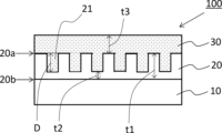
- FIG. 1 is a cross-sectional view illustrating an embodiment of an optical element according to the present disclosure.
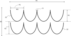
- FIG. 2 is a plan view for explaining an embodiment in which a plurality of recesses having a first shape are arranged in a first surface.
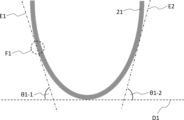
- FIG. 13 is a schematic plan view for explaining a method for calculating a local angle under condition 1.
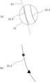
- Fig. 4A is a schematic plan view for explaining the locations where tangent lines are drawn under condition 1.
- Fig. 4B is a schematic plan view for explaining continuous changes in local angles under condition 1.
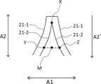
- FIG. 13 is a schematic plan view for explaining a method for calculating a local angle under condition 2.
- 6 is a diagram showing symbols X, Y, and Z in FIG. 5 .
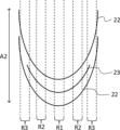
- FIG. 13 is a partial plan view showing an embodiment in which recesses of a second shape are arranged between recesses of a first shape arranged at a predetermined pitch in a second direction.
- the optical element of the present disclosure comprises: A pattern layer and a liquid crystal layer, the pattern layer has a first surface and a second surface opposite the first surface; the liquid crystal layer is formed on the first surface of the patterned layer; the pattern layer has a plurality of recesses of a first shape in the first surface; the first shape recess has an arc shape in a plan view, the recesses of the first shape are disposed continuously at a predetermined pitch in a first direction in the first plane, and ends of the recesses of the first shape adjacent to each other in the first direction are joined to each other; The recess of the first shape satisfies the following conditions 1 and 2.
- the angle between a tangent to the arc shape of the recess of the first shape and a parallel line in the first direction is defined as a local angle of the recess of the first shape.
- the recess of the first shape has a minimum value of the local angle that is greater than ⁇ 90.0 degrees and equal to or less than ⁇ 80.0 degrees, a maximum value of the local angle that is equal to or greater than +80.0 degrees and less than +90.0 degrees, and the local angle changes continuously from the minimum value to the maximum value.
- a direction perpendicular to the first direction is defined as a second direction
- a direction in which the arc of the arc shape is convex is defined as a second' direction
- a point where the ends of adjacent recesses of the first shape are joined is defined as a junction point X
- a point 100 nm away from the junction point X in the second' direction is defined as a point M.
- intersections of a straight line drawn in the first direction from point M with the recess of one first shape forming junction point X and the recess of the other first shape are defined as intersection Y and intersection Z, respectively.
- the average angle between a first line connecting the junction point X and the intersection point Y and a second line connecting the junction point X and the intersection point Z is greater than 0 degrees and equal to or less than 20.0 degrees.
- FIG. 1 is a cross-sectional view showing one embodiment of an optical element according to the present disclosure.
- the optical element 100 in Fig. 1 has a pattern layer 20 and a liquid crystal layer 30.
- the pattern layer 20 has a first surface 20a and a second surface 20b opposite to the first surface.
- the liquid crystal layer 30 is formed on the first surface 20a of the pattern layer 20.
- the pattern layer 20 has a plurality of recesses 21 on the first surface 20a.
- the optical element 100 in Fig. 1 has a substrate 10 on the side of the pattern layer 20 opposite to the liquid crystal layer 30.
- the reference character D indicates the depth of the recess.
- Fig. 1 the reference character D indicates the depth of the recess.
- the reference character t1 indicates the thickness of the pattern layer at a location that does not have a recess.
- the reference character t2 indicates the thickness of the pattern layer below the recess.
- the reference character t3 indicates the thickness of the liquid crystal layer formed at a location that does not have a recess.
- Fig. 1 is a schematic cross-sectional view. That is, the scale of each layer constituting the optical element 100 and the scale of the recessed portion on the first surface are schematic for ease of illustration and differ from the actual scale. The same applies to other figures besides Fig. 1.
- the pattern layer has a first surface and a second surface opposite to the first surface.
- a liquid crystal layer is formed on the first surface of the pattern layer.
- a liquid crystal layer 30 is disposed within the recesses 21 of the patterned layer.
- the shape of the second surface 20b of the pattern layer is not particularly limited. In order to improve the adhesion between the second surface side of the pattern layer and other members such as a substrate, the second surface of the pattern layer is preferably flat.
- FIG. 2 is a plan view for explaining an embodiment in which a plurality of recesses 22 having a first shape are arranged in a first surface.
- A1 indicates a first direction
- A2 indicates a second direction perpendicular to the first direction
- P1 indicates the pitch of the recesses of the first shape in the first direction
- W1 indicates the length of the recesses of the first shape in the first direction
- P2 indicates the pitch of the recesses of the first shape in the second direction
- H1 indicates the length of the recesses of the first shape in the second direction. Since the ends of the recesses of the first shape are joined in the first direction, W1 and P1 are equal.
- the first-shaped recesses 22 are continuously arranged at a pitch P1 in the first direction A1.
- the first-shaped recesses 22 adjacent to each other in the first direction A1 have a joint point X where their ends are joined (the symbol "X" of the joint point is omitted in Fig. 2).
- the first-shaped recesses 22 are arranged at a pitch P2 in the second direction A2.
- the first-shaped recesses 22 are not joined in the second direction.
- the pattern layer must have a plurality of recesses of a first shape in the first surface, and the recesses of the first shape must have an arc shape in a plan view.
- the liquid crystal in the liquid crystal layer is aligned along the shape of the pattern layer, so by forming the recesses of the first shape in an arc shape, the liquid crystal in the liquid crystal layer can be easily aligned in an arc shape in the first direction.
- the pattern layer requires that the recesses of the first shape are continuously arranged at a predetermined pitch in a first direction within the first surface, and that adjacent recesses of the first shape in the first direction have their ends joined together.
- the liquid crystal molecules in the liquid crystal layer are more likely to be aligned when there are no gaps in the pattern of the pattern layer. Therefore, by joining adjacent recesses of the first shape, the liquid crystal molecules in the liquid crystal layer can be more easily aligned.
- the concave portion of the first shape must satisfy the following condition 1.
- Condition 1 The angle between a tangent to the arc shape of the recess of the first shape and a parallel line in the first direction is defined as a local angle of the recess of the first shape.
- the recess of the first shape has a minimum value of the local angle that is greater than ⁇ 90.0 degrees and equal to or less than ⁇ 80.0 degrees, a maximum value of the local angle that is equal to or greater than +80.0 degrees and less than +90.0 degrees, and the local angle changes continuously from the minimum value to the maximum value.
- FIG. 3 is a schematic plan view for explaining a method of calculating a local angle under condition 1.
- reference numeral 21 denotes a recess having a first shape
- dashed line D1 denotes a parallel line in a first direction
- dashed lines E1 and E2 denote tangents to the arc shape of the recess having the first shape.
- Fig. 4(a) is a schematic plan view for explaining the location where the tangent line is drawn under condition 1.
- Fig. 4(a) is also a partial enlarged view of the planar shape of the arc shape of the first shape recess (partial enlarged view of the location indicated by reference symbol F1 in Fig. 3).
- the arc shape includes a first arc 21-1 on the inner periphery side, a second arc 21-2 on the outer periphery side, and a line connecting the ends of the first arc and the second arc on the same side. Under condition 1, the tangent line to the arc shape is drawn so as to be tangent to the arc 21-2 on the outer periphery side.
- condition 1 and condition 3 described below the signs of "-" and "+” for local angles are determined by using the perpendicular direction to the parallel lines in the first direction as a reference, with a "-" sign for the angle between a tangent line inclined to one side with respect to the reference and a parallel line in the first direction, and a "+” sign for the angle between a tangent line inclined to the other side with respect to the reference and a parallel line in the first direction.
- the tangent line forming ⁇ 1-1 and the tangent line forming ⁇ 1-2 are inclined to different sides with respect to the reference. Therefore, if the sign of ⁇ 1-1 is "-”, the sign of ⁇ 1-2 is "+".
- Satisfying condition 1 means that the arc-shaped recesses are continuous in a semicircular shape without being interrupted along the way. Since the optical element of the present disclosure satisfies condition 1, the pitch of the recesses of the first shape can be easily increased in the first direction. Furthermore, since the optical element of the present disclosure has the ends of adjacent recesses of the first shape joined in the first direction, there is no gap between adjacent recesses of the first shape. Therefore, the optical element of the present disclosure can easily align liquid crystal molecules along the recesses of the first shape in the first direction.
- the acute angle is regarded as a local angle of the recess of the first shape.
- the minimum value of the local angle is preferably ⁇ 89.7 degrees or more and ⁇ 81.0 degrees or less, more preferably ⁇ 89.5 degrees or more and ⁇ 82.0 degrees or less, and even more preferably ⁇ 89.0 degrees or more and ⁇ 83.0 degrees or less.
- the maximum value of the local angle is preferably +81.0 degrees or more and +89.7 degrees or less, more preferably +82.0 degrees or more and +89.5 degrees or less, and even more preferably +83.0 degrees or more and +89.0 degrees or less.
- the planar shape of the recesses on the first surface of the pattern layer is confirmed by photographing the first surface of the pattern layer with a scanning electron microscope.
- the local angle in Condition 1 is calculated from the photograph.
- the scanning electron microscope is preferably used for imaging under the following conditions:
- the scanning electron microscope may be SU8000, a product name of Hitachi High-Technologies Corporation.
- Condenser lens 2 1.0 ⁇ Tilt function of the document table: Enter the tilt angle "0.0"
- condition 1 whether or not the local angle changes continuously can be determined by the following (1) to (3).
- tangent lines are drawn to calculate the local angles. For example, at the points marked with " ⁇ " and " ⁇ " in FIG. 4B, tangent lines are drawn to calculate the local angles. If the local angles are the same down to the first decimal place, the relationship between the two points is defined as "satisfying the relationship of continuous tangents.”
- the relationship between the two points is defined as "satisfying the relationship of continuous tangents.”
- the distance between the two points is less than 10 nm, it is considered that the "local angle changes continuously" between these two points. (For example, if the local angles of " ⁇ " and " ⁇ " in FIG.
- the concave portion of the first shape must satisfy the following condition 2.
- Condition 2 A direction perpendicular to the first direction is defined as a second direction, a direction in which the arc of the arc shape is convex is defined as a second' direction, a point where the ends of adjacent recesses of the first shape are joined is defined as a junction point X, and a point 100 nm away from the junction point X in the second' direction is defined as a point M.
- the intersections of a straight line drawn in the first direction from point M with the recess of one first shape forming junction point X and the recess of the other first shape are defined as intersection Y and intersection Z, respectively.
- the average angle between a first line connecting the junction point X and the intersection point Y and a second line connecting the junction point X and the intersection point Z is greater than 0 degrees and equal to or less than 20.0 degrees.
- Fig. 5 is a schematic plan view for explaining a method of calculating the angle of condition 2.
- Fig. 5 is also a partial enlarged view of the portion indicated by reference symbol C1 in Fig. 2.
- Fig. 6 is a view in which reference symbols X, Y, and Z are extracted from Fig. 5.
- the angle formed by a first straight line connecting the junction point X and the intersection point Y and a second straight line connecting the junction point X and the intersection point Z corresponds to ⁇ in Fig. 6.
- the symbol A2 indicates the second direction
- the symbol A2' indicates the second direction in which the arc of the arc shape is convex
- the symbol A1 indicates the first direction.
- the symbol X indicates a joining point under condition 2.
- the joining point under condition 2 means a location where arcs 21-2 on the outer periphery join together, as shown in FIG. Although not shown, in FIG. 5, the distance between the symbol X and the symbol M is 100 nm.
- the angle between a first line connecting the junction point X and the intersection point Y and a second line connecting the junction point X and the intersection point Z is calculated at any 20 points. The average of the angles at the 20 points is set as the average angle for condition 2.
- the average angle of condition 2 When the average angle of condition 2 is 0 degrees, the ends of the recesses of the first shape can be brought close to the limit in the first direction. However, when the average angle of condition 2 is 0 degrees, the accuracy of the pattern near the junction is likely to decrease when preparing a plate for forming the pattern layer, so the pattern layer cannot be stably formed. Therefore, when the average angle of condition 2 is 0 degrees, it is difficult to fully demonstrate the performance of the optical element. Furthermore, when the average angle of condition 2 is 0 degrees, adjacent recesses are integrated near the junction, so the width of the recesses becomes wider. Therefore, when the average angle of condition 2 is 0 degrees, it is difficult for liquid crystal molecules to be oriented along the recesses near the junction.
- the average angle of condition 2 exceeds 20.0 degrees, the load near the joining point increases when the pattern layer is peeled off from the shaping plate, and the pattern layer is likely to deform. Therefore, if the average angle of condition 2 exceeds 20.0 degrees, it is difficult to fully exhibit the performance of the optical element.
- the average angle of Condition 2 is set to be greater than 0 degrees and equal to or less than 20.0 degrees, the pattern layer can be formed stably, and the performance of the optical element can be fully exhibited.
- the lower limit of the average angle in condition 2 is preferably 0.5 degrees or more, more preferably 1.0 degrees or more, and even more preferably 2.0 degrees or more, and the upper limit is preferably 15.0 degrees or less, more preferably 12.0 degrees or less, and even more preferably 6.0 degrees or less.
- a numerical range can be set by combining one selected from the upper limit options with one selected from the lower limit options.
- examples of numerical ranges include: more than 0 degrees and less than 20.0 degrees, more than 0 degrees and less than 15.0 degrees, more than 0 degrees and less than 12.0 degrees, more than 0 degrees and less than 6.0 degrees, 0.5 degrees or more and less than 20.0 degrees, 0.5 degrees or more and less than 15.0 degrees, 0.5 degrees or more and less than 12.0 degrees, 0.5 degrees or more and less than 6.0 degrees, 1.0 degrees or more and less than 20.0 degrees, 1.0 degrees or more and less than 15.0 degrees, 1.0 degrees or more and less than 12.0 degrees, 1.0 degrees or more and less than 6.0 degrees, 2.0 degrees or more and less than 20.0 degrees, 2.0 degrees or more and less than 15.0 degrees, 2.0 degrees or more and less than 12.0 degrees, and 2.0 degrees or more and less than and less than 6.0 degrees, 2.0 degrees or more and less than 20.0 degrees, 2.0 degrees or more and less than 15.0 degrees, 2.0 degrees or more and
- the pitch P1 of the recesses of the first shape in the first direction varies depending on the optical properties to be desired, but is preferably 0.4 ⁇ m to 10,000 ⁇ m, more preferably 0.7 ⁇ m to 8,000 ⁇ m, and even more preferably 1.0 ⁇ m to 6,000 ⁇ m.
- the pitch P1 of the recesses of the first shape in the first direction is the same as the length W1 of the recesses of the first shape in the first direction. For this reason, it is preferable that W1 is also in the range described above.
- Setting P1 to 0.4 ⁇ m or more is preferable in that it makes it easier to align the liquid crystal molecules and obtains optical characteristics of blue (wavelength 450 nm) which is on the short wavelength side of the visible light region.
- the pitch of the recesses and the length of the recesses are measured from a photograph of the first surface of the pattern layer taken with a scanning electron microscope.
- the length H1 of the first shaped recess in the second direction cannot be generally determined because it varies depending on the desired optical properties, but is preferably 0.1 ⁇ m or more and 20,000 ⁇ m or less, more preferably 0.2 ⁇ m or more and 18,000 ⁇ m or less, and even more preferably 0.3 ⁇ m or more and 17,000 ⁇ m or less. It is preferable to set H1 to 0.1 ⁇ m or more in that this makes it easier to align the liquid crystal molecules.
- the ratio (H1/W1) of the length H1 of the first shape recess in the second direction to the length W1 of the first shape recess in the first direction is preferably 0.3 to 2.0, more preferably 0.4 to 1.9, and even more preferably 0.5 to 1.8.
- the distance between the first arc 21-1 (arc on the inner periphery) and the second arc 21-2 (arc on the outer periphery) is preferably 1 nm or more and 100 nm or less, more preferably 5 nm or more and 50 nm or less, and even more preferably 15 nm or more and 30 nm or less.
- the distance between 1 nm or more the pattern layer can be more easily peeled off from the shaping plate, and the pattern layer can be more stably formed.
- the distance to 100 nm or less the liquid crystal molecules can be more easily aligned.
- the distance between the first arc and the second arc is determined as the average value of distances at any 20 points in a photograph of the first surface of the pattern layer taken with a scanning electron microscope.
- the depth of the recess of the first shape is preferably 2 nm or more and 200 nm or less, more preferably 10 nm or more and 100 nm or less, and further preferably 20 nm or more and 50 nm or less.
- the liquid crystal molecules can be more easily aligned along the recesses.
- the pattern layer can be more easily peeled off from the shaping plate, so that the pattern layer can be more stably formed.
- the depth of other recesses such as the recesses of the second shape is also preferably within the above range.
- the depth of the recess of the first shape is defined as the average value of 18 depth values, excluding the maximum and minimum values, from 20 depth values of the recess randomly selected.
- the depths of the other recesses, such as the recess of the second shape are also defined as the average value obtained by the above-mentioned method.
- the depth of the recesses such as the recesses of the first shape is measured by imaging a vertical cross section of the optical element with a scanning electron microscope.
- the depth of each recess means the maximum depth of each recess.
- the scanning electron microscope is preferably used for imaging under the following conditions.
- An example of the scanning electron microscope is the product name "SU8000" of Hitachi High-Technologies Corporation. ⁇ Imaging conditions> Acceleration voltage: 5.0 kV Emission current: 5.0 ⁇ A ⁇ Probe current: High ⁇ Detector: SE(U) ⁇ WD: 8mm Condenser lens 1:5.0 Condenser lens 2: 1.0 ⁇ Tilt function of the document table: Enter the tilt angle "0.0"
- the recesses of the first shape are further arranged at a predetermined pitch in the second direction. 2, the recesses 22 of the first shape are arranged at a pitch P2 in the second direction A2.
- the recesses of the first shape are not joined in the second direction in order to stably form the pattern layer.
- the pitch P2 is preferably 0.1 ⁇ m or more and 100.0 ⁇ m or less, more preferably 0.15 ⁇ m or more and 60.0 ⁇ m or less, and further preferably 0.3 ⁇ m or more and 20.0 ⁇ m or less.
- recesses of a second shape that satisfy the following conditions (1) to (4) are disposed between the recesses of the first shape that are disposed at a predetermined pitch in the second direction.
- the recess of the second shape has an arc shape in a plan view.
- the recesses of the second shape are arranged at a predetermined pitch in the first direction.
- the length of the recess having the second shape in the first direction is shorter than the length of the recess having the first shape in the first direction.
- the ends of the recesses of the second shape adjacent to each other in the first direction are not joined to each other.
- FIG. 7 is a partial plan view showing an embodiment in which recesses 23 of a second shape are arranged between recesses 22 of a first shape arranged at a predetermined pitch in the second direction A2.
- the density of the recesses in the first surface of the pattern layer can be increased, and therefore the area that exerts a predetermined function can be increased in the surface of the optical element.
- the arc shape of the recess of the second shape preferably coincides with a portion of the arc shape of the recess of the first shape.
- the coincidence of the arc shape of the recess of the second shape with a part of the arc shape of the recess of the first shape is determined from a photograph of the first surface of the pattern layer taken with a scanning electron microscope. For example, the determination can be made by the following steps A1 to A3.
- A1 A portion corresponding to the arc shape of the recess of the second shape is cut out from the image data of the photograph.
- A2 When the arc shape of the cut recess of the second shape is moved in the second direction, the area ratio of the overlapping area of the arc shape of the recess of the second shape and the arc shape of the recess of the first shape is calculated.
- the area ratio is expressed by the following formula.
- Area ratio (%) (area of the portion of the arc shape of the recess of the second shape that overlaps with the arc shape of the recess of the first shape/area of the arc shape of the recess of the second shape) ⁇ 100
- A3 When the area ratio is 90% or more, it is considered that the arc shape of the recess of the second shape coincides with a part of the arc shape of the recess of the first shape.
- the length of the recesses of the second shape in the first direction may be adjusted to match the desired density of the recesses, within a range shorter than the length of the recesses of the first shape in the first direction.
- the optical element of the present disclosure may further include, in addition to the second shaped recesses, recesses of a third shape and recesses of a fourth shape, etc., arranged between the first shaped recesses arranged at a predetermined pitch in the second direction. It is preferable that the recess of the nth shape satisfies the following condition ("n" is an integer of 3 or more). "Agreement” in the following (5) means that the area ratio of the following formula is 90% or more.
- Area ratio (%) (area of the portion of the arc shape of the nth shape of the recess that overlaps with the arc shape of the (n-1)th shape of the recess/area of the arc shape of the nth shape of the recess) ⁇ 100 ⁇ Conditions for the nth Shape of the Recess>
- the recess of the nth shape has an arc shape in a plan view.
- the recesses of the nth shape are arranged at a predetermined pitch in the first direction.
- the length in the first direction of the recess having the nth shape is shorter than the length in the first direction of the recess having the (n-1)th shape.
- the ends of the nth recesses adjacent to each other in the first direction are not joined to each other.
- the arc shape of the recess of the nth shape coincides with a portion of the arc shape of the recess of the (n-1)th shape.
- the optical element of the present disclosure further satisfies the following condition 3.
- ⁇ Condition 3> The angle between a tangent to the arc shape of the recess of the first shape and a parallel line in the first direction is defined as a local angle of the recess of the first shape.
- the first surface is divided parallel to the second direction into three regions: a first region where the local angle is -5.0 degrees or more and +5.0 degrees or less, a second region where the local angle is -50.0 degrees or more and -40.0 degrees or less and +40.0 degrees or more and +50.0 degrees or less, and a third region where the local angle is -80.0 degrees or more and -70.0 degrees or less and +70.0 degrees or more and +80.0 degrees or less.
- the sum of the areas of the recesses in the first region relative to the total area of the first region is defined as the "first area ratio”
- the sum of the areas of the recesses in the second region relative to the total area of the second region is defined as the “second area ratio”
- the sum of the areas of the recesses in the third region relative to the total area of the third region is defined as the “third area ratio”
- the difference between the maximum and minimum values of the first area ratio, second area ratio, and third area ratio is 10% or less.
- the total area of the recesses means the total area of all the recesses.
- the total area of all the recesses means the sum of the area of the recesses of the first shape and the area of the recesses other than the recesses of the first shape.
- Satisfying condition 3 means that there is little difference in the area ratio of the recesses between regions. By satisfying condition 3, it becomes easier to stably exhibit the specified performance within the surface of the optical element. In condition 3, it is more preferable that the difference between the maximum and minimum values is 7% or less, and even more preferable that it is 5% or less.
- the area ratios of 1 to 3 are measured from a photograph of the first surface of the pattern layer taken with a scanning electron microscope. More specifically, the area ratios of 1 to 3 are calculated at any 20 points on the photograph, and the average value of the 20 points is taken as the area ratios of 1 to 3.
- the pattern layer may have a thickness below the recess.
- the symbol t2 indicates the thickness of the pattern layer below the recess.
- the average thickness below the recess is preferably 0.5 ⁇ m to 20 ⁇ m, more preferably 1 ⁇ m to 15 ⁇ m, and even more preferably 2 ⁇ m to 7 ⁇ m.
- t2 By setting t2 to 0.5 ⁇ m or more, it is possible to easily control the curing when forming the pattern layer, and it is also possible to easily apply the liquid crystal layer onto the pattern layer.
- the average thickness below the recess means the average thickness of 8 points excluding the maximum and minimum values from among 10 arbitrary points on the cross-sectional photograph of the optical element.
- the pattern layer preferably contains a resin.
- the proportion of the resin in the pattern layer is preferably 50% by mass or more, more preferably 70% by mass or more, and even more preferably 90% by mass or more, based on the total solid content of the pattern layer.
- the resin for the pattern layer examples include a thermoplastic resin and a cured product of a curable resin composition. Among these, a cured product of a curable resin composition is preferred in order to improve strength.
- the proportion of the cured product of the curable resin composition is preferably 50% by mass or more, more preferably 70% by mass or more, and even more preferably 90% by mass or more, based on the total solid content of the pattern layer.
- Examples of the cured product of the curable resin composition include a cured product of a heat-curable resin composition and a cured product of an ionizing radiation-curable resin composition, and among these, a cured product of an ionizing radiation-curable resin composition is preferred.
- the ionizing radiation curable resin composition is a composition containing a compound having an ionizing radiation curable functional group (hereinafter, also referred to as an "ionizing radiation curable compound").
- a compound having an ionizing radiation curable functional group hereinafter, also referred to as an "ionizing radiation curable compound”
- the ionizing radiation curable functional group include ethylenically unsaturated bond groups such as (meth)acryloyl groups, vinyl groups, and allyl groups, as well as epoxy groups and oxetanyl groups.
- a compound having an ethylenically unsaturated bond group is preferred.
- a compound having two or more ethylenically unsaturated bond groups is more preferred, and among them, a polyfunctional (meth)acrylate compound having two or more ethylenically unsaturated bond groups is even more preferred.
- the polyfunctional (meth)acrylate compound both monomers and oligomers can be used.
- the ionizing radiation refers to electromagnetic waves or charged particle beams that have an energy quantum capable of polymerizing or crosslinking molecules.
- UV ultraviolet rays
- EB electron beams
- electromagnetic waves such as X-rays and gamma rays
- charged particle beams such as alpha rays and ion beams
- examples of bifunctional (meth)acrylate monomers include ethylene glycol di(meth)acrylate, bisphenol A tetraethoxydiacrylate, bisphenol A tetrapropoxydiacrylate, and 1,6-hexanediol diacrylate.
- trifunctional or higher (meth)acrylate monomers examples include trimethylolpropane tri(meth)acrylate, pentaerythritol tri(meth)acrylate, pentaerythritol tetra(meth)acrylate, dipentaerythritol hexa(meth)acrylate, dipentaerythritol tetra(meth)acrylate, and isocyanuric acid-modified tri(meth)acrylate.
- the (meth)acrylate monomer may have a part of its molecular skeleton modified, and those modified with ethylene oxide, propylene oxide, caprolactone, isocyanuric acid, alkyl, cyclic alkyl, aromatic, bisphenol, or the like may also be used.
- polyfunctional (meth)acrylate oligomer examples include acrylate polymers such as urethane (meth)acrylate, epoxy (meth)acrylate, polyester (meth)acrylate, and polyether (meth)acrylate.
- the urethane (meth)acrylate can be obtained, for example, by reacting a polyhydric alcohol and an organic diisocyanate with a hydroxy (meth)acrylate.
- Preferred epoxy (meth)acrylates are (meth)acrylates obtained by reacting a tri- or higher functional aromatic epoxy resin, alicyclic epoxy resin, aliphatic epoxy resin, or the like with (meth)acrylic acid, (meth)acrylates obtained by reacting a di- or higher functional aromatic epoxy resin, alicyclic epoxy resin, aliphatic epoxy resin, or the like with a polybasic acid and (meth)acrylic acid, and (meth)acrylates obtained by reacting a di- or higher functional aromatic epoxy resin, alicyclic epoxy resin, aliphatic epoxy resin, or the like with a phenol and (meth)acrylic acid.
- the above ionizing radiation curable resins may be used alone or in combination of two or more.
- the coating liquid for forming the pattern layer preferably contains additives such as a photopolymerization initiator and a photopolymerization accelerator.
- the photopolymerization initiator may be one or more selected from acetophenone, benzophenone, ⁇ -hydroxyalkylphenone, Michler's ketone, benzoin, benzyl dimethyl ketal, benzoyl benzoate, ⁇ -acyloxime ester, thioxanthones, and the like.
- the photopolymerization accelerator can reduce polymerization inhibition caused by air during curing and increase the curing speed
- examples of the accelerator include one or more types selected from p-dimethylaminobenzoic acid isoamyl ester, p-dimethylaminobenzoic acid ethyl ester, and the like.
- the pattern layer may contain additives such as refractive index adjusters, antioxidants, UV absorbers, light stabilizers, and antistatic agents, to the extent that they do not impair the effects of the present disclosure.
- the pattern layer can be formed, for example, by shaping the unshaped pattern layer using a plate having a shape complementary to the surface shape of the first surface. More specifically, the pattern layer can be formed, for example, by the following steps 1 and 2.
- Step 1 A step of applying a coating liquid for forming a pattern layer containing a resin onto a substrate to form a layer containing a resin.
- Step 2 A step of shaping a layer containing a resin using a plate having a shape complementary to the surface shape of the first surface of the pattern layer.
- the coating liquid for forming the pattern layer contains a solvent, it is preferable to dry the solvent in step 1.
- a curable resin When a curable resin is used as the resin, it is preferable to use a pattern layer forming coating liquid containing a curable resin composition as the pattern layer forming coating liquid in step 1. That is, when a curable resin is used as the resin, it is preferable that the curable resin in the coating liquid in step 1 is in an uncured state.
- a coating liquid for forming a pattern layer containing an ionizing radiation curable resin composition is used as the coating liquid for forming a pattern layer in step 1, it is preferable to irradiate ionizing radiation simultaneously with the shaping in step 2 to cure the ionizing radiation curable resin composition contained in the shaped layer.
- step 1 If there is another layer, such as a primer layer, between the substrate and the pattern layer, it is preferable to carry out a step of forming the other layer on the substrate before step 1.
- a primer layer such as a primer layer
- the plate used in step 2 can be produced by a general-purpose means such as laser lithography, electron beam lithography, FIB (Focused Ion Beam), etc. It is also preferable to produce a large number of plates by duplicating the plate produced by the above-mentioned means, and arrange the many copies to form a multi-faceted plate.
- the plate duplication can be carried out by a general-purpose means such as electroforming.
- the shape of the plate may be flat, cylindrical, etc. A cylindrical plate is preferred in that it can be processed by roll-to-roll and has excellent productivity.
- a liquid crystal layer is formed on the first surface of the pattern layer.
- the liquid crystal layer can be formed, for example, by applying a liquid crystal layer-forming coating liquid containing a liquid crystal compound onto the pattern layer, and then drying and curing the liquid crystal layer as necessary.
- the liquid crystal compound may be at least one selected from rod-shaped liquid crystal compounds such as nematic liquid crystal compounds and smectic liquid crystal compounds, cholesteric liquid crystal compounds, and discotic liquid crystal compounds (disk-shaped liquid crystal compounds).
- the liquid crystal layer may further contain a chiral agent in addition to the liquid crystal compound.
- a liquid crystal layer containing a nematic liquid crystal compound and a chiral agent has an arrangement in which the direction of the molecules of the liquid crystal compound rotates when the liquid crystal layer is viewed in a plane.
- the direction of the molecules of the liquid crystal compound does not need to rotate 360 degrees, and may rotate less than 360 degrees.
- the liquid crystal compound is preferably a rod-shaped liquid crystal compound.
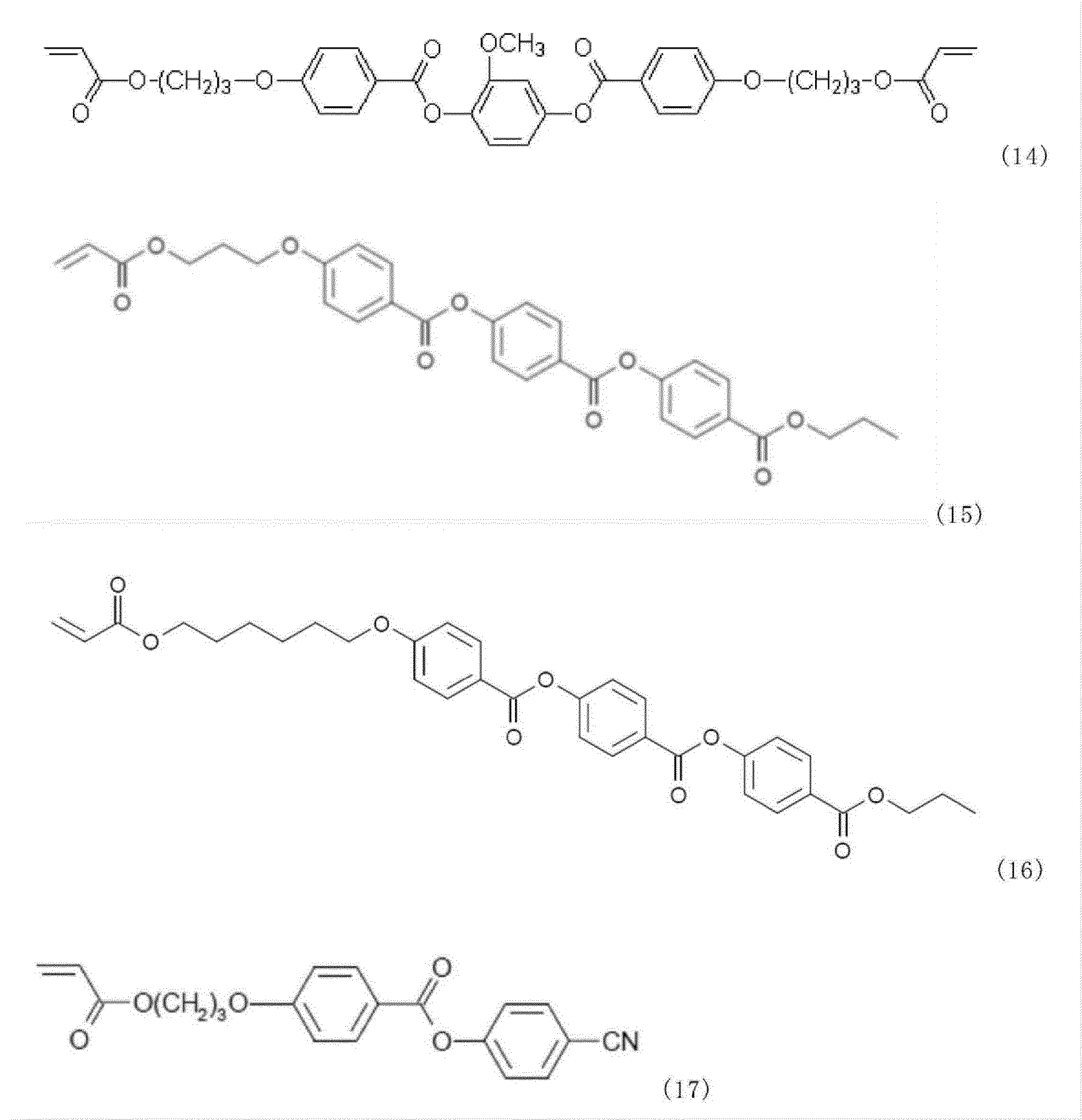
- the rod-shaped liquid crystal compound there are no particular limitations on the rod-shaped liquid crystal compound, but examples include the compounds shown in (1) to (17) below.
- polymerizable rod-shaped liquid crystal materials are preferred.
- polymerizable functional groups in polymerizable rod-shaped liquid crystal materials include those that polymerize due to the action of ionizing radiation such as ultraviolet light or electron beams, or heat.
- Specific examples include radically polymerizable functional groups.
- examples of radically polymerizable functional groups include functional groups that have at least one ethylenically unsaturated double bond capable of addition polymerization, and more specifically, examples of radically polymerizable functional groups include vinyl groups and acrylate groups (a general term that includes acryloyl groups, methacryloyl groups, acryloyloxy groups, and methacryloyloxy groups) with or without substituents.
- the liquid crystal layer is preferably formed on the entire surface of the first surface of the pattern layer, that is, the liquid crystal layer is preferably formed also on the portions of the first surface of the pattern layer that do not have recesses (FIG. 1).
- the thickness of the liquid crystal compound may be adjusted according to the desired retardation value.
- the liquid crystal layer may be of a single layer structure or a multi-layer structure, but in order to reduce the thickness, the liquid crystal layer is preferably of a single layer structure. In order to improve the display quality by broadening the bandwidth of the optical element, it is preferable that the liquid crystal layer satisfies the following condition (i) or (ii). (i) The liquid crystal layer has a multi-layer structure and has positive wavelength dispersion. (ii) The liquid crystal layer has a single layer structure and has negative wavelength dispersion.
- the liquid crystal layer may have positive wavelength dispersion or negative wavelength dispersion.
- Negative wavelength dispersion is a characteristic in which the phase difference imparted to transmitted light increases as the wavelength of the transmitted light becomes longer.
- Positive wavelength dispersion is a characteristic in which the phase difference imparted to transmitted light decreases as the wavelength of the transmitted light becomes longer.
- Re450 in-plane phase difference at a wavelength of 450 nm
- Re550 in-plane phase difference at a wavelength of 550 nm
- the characteristic of Re450 ⁇ Re550 is referred to as negative wavelength dispersion.
- the characteristic of Re450>Re550 is referred to as positive wavelength dispersion.
- the shape of the pattern layer can be confirmed, for example, by the following method (1) or (2).
- the shape of the pattern layer may be confirmed by a method other than the following methods (1) and (2) as long as the method can easily remove the liquid crystal layer on the pattern layer.
- (1) According to JIS K5600-5-6:1999, 100 grid cuts are made at 1 mm intervals on the surface of the liquid crystal layer. Then, 18 mm Cellophane Tape (registered trademark) manufactured by Nichiban Co., Ltd. is applied to the cuts, and the tape is firmly attached to the coating film by rubbing it with an eraser. The tape is then instantly peeled off at least 10 times to peel off the coating film.
- part of the coating film of the grid cuts peels off during the above-mentioned operation, it is preferable to repeat the above-mentioned operation with the peeled part as the center. In this way, the shape of the pattern layer can be confirmed by peeling off the liquid crystal layer on the pattern layer.
- the optical element is cut as thin as possible and cross-sectional STEM images are taken repeatedly. The cross-sectional STEM images obtained are stitched together to create a 3D image, allowing the shape of the pattern layer to be confirmed.
- the optical element of the present disclosure may have a substrate.
- the material constituting the substrate can be used as the material constituting the substrate, but materials having good mechanical properties, optical properties, stability and processability are preferred.
- materials having good mechanical properties, optical properties, stability and processability include polymer resins having an alicyclic structure, methacrylic resins, polycarbonate resins, polystyrene resins, acrylonitrile-styrene copolymers, methyl methacrylate-styrene copolymers, ABS resins, polyethersulfone, triacetyl cellulose, polyethylene terephthalate, epoxy acrylate, urethane acrylate, and other resins; glass; and the like, with resins being preferred.
- the substrate is preferably a resin substrate.
- the in-plane retardation of the substrate is preferably 20 nm or less, more preferably 5 nm or less, even more preferably 3 nm or less, even more preferably 1 nm or less, and most preferably 0 nm.
- the wavelength ⁇ of light serving as the reference for the retardation is 550 nm.
- the thickness of the substrate can be appropriately adjusted within the range of 5 ⁇ m or more and 1000 ⁇ m or less.
- the thickness of the substrate can be measured by a film thickness measuring device.
- film thickness measuring devices include Mitutoyo's Digimatic Standard Outside Micrometer (product number: MDC-25SX).
- the thickness of the substrate may be determined by measuring any ten points and averaging the measured value as described above.
- the substrate preferably has a total light transmittance according to JIS K7361-1:1997 of 70% or more, more preferably 80% or more, and even more preferably 85% or more.
- the substrate preferably has a haze according to JIS K7136:2000 of 10% or less, more preferably 5% or less, and even more preferably 3% or less.
- the refractive index of the pattern layer and the refractive index of the substrate are close in value.
- the refractive index of the pattern layer/refractive index of the substrate is preferably 0.97 or more and 1.03 or less, and more preferably 0.99 or more and 1.01 or less.
- the wavelength ⁇ of light that is the basis for the refractive index is 550 nm.
- the optical element of the present disclosure may further include other layers.
- other layers include a primer layer for improving adhesion between the substrate and the pattern layer, an antistatic layer, etc.
- the primer layer is preferably formed between the substrate and the pattern layer, and the antistatic layer is preferably formed on the substrate opposite to the pattern layer.
- the optical element may have an average in-plane retardation within a predetermined range.
- the in-plane retardation of the optical element is preferably ( ⁇ /2) ⁇ 0.95 or more and ( ⁇ /2) ⁇ 1.05 or less, more preferably ( ⁇ /2) ⁇ 0.97 or more and ( ⁇ /2) ⁇ 1.03 or less, and more preferably ( ⁇ /2) ⁇ 0.99 or more and ( ⁇ /2) ⁇ 1.01 or less.
- the in-plane retardation of an optical element means the average value of five in-plane retardations excluding the maximum and minimum values from among the seven in-plane retardations in the plane of the optical element.
- the wavelength ⁇ of light serving as the reference for the retardation is 550 nm.
- measuring devices for the in-plane retardation include "AxoStep” manufactured by AXOMETRICS and a two-dimensional birefringence evaluation system (product name: WPA-Micro) manufactured by Photonic Lattice.
- the former product is suitable for measuring a wide area, and the latter product is suitable for measuring a narrow area.
- the optical element of the present disclosure can be used, for example, as a diffractive optical element.
- the optical element of the present disclosure can also be used as a component of a light control device.
- the diffraction angle of light transmitted through a diffractive optical element can be adjusted to a predetermined range, so that, for example, the irradiation range of light can be widened or narrowed by using a diffractive optical element.
- the diffractive optical element can be used as a component of devices such as cross reality, optical sensors, and laser projectors.
- the diffraction angle ⁇ of the diffractive optical element can be expressed by the following formula, where the pitch is x [nm], the wavelength of light is ⁇ [nm], and the incident angle of light is ⁇ 0.
- ⁇ and ⁇ 0 are angles when the perpendicular direction to the plane of the diffractive optical element is 0 degrees.
- ⁇ 0 is the case of a positive direction from the perpendicular direction.
- the sign ⁇ is added because, depending on the rotation direction of the circularly polarized light that is the incident light, there are cases where the light is diffracted in the positive direction or the negative direction with respect to the perpendicular direction.
- the diffraction angles in Table 1 are angles when there is one diffractive optical element. If the polarization state is the same, increasing the number of diffractive optical elements increases the diffraction angle as a multiplier of the number of diffractive optical elements. If the diffraction angle at an arbitrary pitch is ⁇ (degrees) and the number of diffractive optical elements is n, the diffraction angle can be expressed as 2 n-1 ⁇ (degrees).
- the first surface of the pattern layer of the intermediate of the optical element of the example and the comparative example was imaged using a scanning electron microscope (Hitachi High-Technologies Corporation, product name "SU8000").
- the imaging conditions were as follows.
- the intermediate means a laminate having a primer layer and a pattern layer on a substrate.
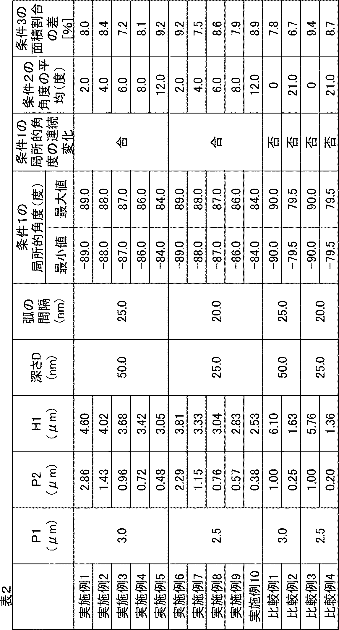
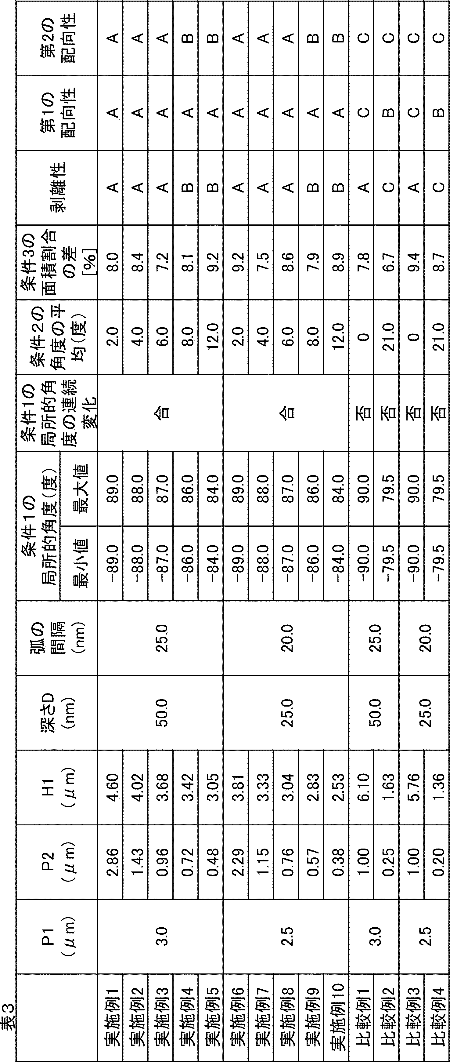
- the local angle of condition 1 the pitch P1 in the first direction, the pitch P2 in the second direction, the length H1 of the recess of the first shape in the second direction, the distance between the first arc and the second arc, the average angle of condition 2, and the difference in the area ratio of condition 3 were calculated by the method described in the specification.
- the peelability was evaluated according to the following criteria, and the results are shown in Table 3.
- D When forming the pattern layer, the shaping plate could not be peeled off from the shaped layer.
- Second Orientation Regarding the optical elements of the examples and comparative examples whether or not the liquid crystal molecules are oriented along the direction of the first-shaped concaves in the vicinity of the junction point X where the ends of the adjacent first-shaped concaves are joined was observed.
- a two-dimensional birefringence evaluation system product name: WPA-Micro
- the second orientation was evaluated according to the following criteria. The second orientation was observed in a narrower area than the first orientation.
- the shape of the first surface of the pattern layer was designed using a simulation tool.
- the first surface was arranged so that the recesses of the first shape were continuously arranged at a predetermined pitch in a first direction, and the recesses of the first shape adjacent in the first direction were joined at their ends. Furthermore, the first surface was arranged so that the recesses of the first shape were arranged at a predetermined pitch in a second direction perpendicular to the first direction.
- the above simulation was performed so that, with respect to the planar shape of the recess of the first shape, the local angle of condition 1, pitch P1 in the first direction, pitch P2 in the second direction, length H1 of the recess of the first shape in the second direction, distance between the first arc and the second arc, average angle of condition 2, and difference in area ratio of condition 3 were the values shown in Table 2. Furthermore, the above simulation was performed so that the planar shape of the recess of the first shape satisfied condition 1. Using a 6-inch square synthetic quartz plate, a quartz master mold with a surface shape designed by simulation was produced by an electron beam lithography process using an electron beam drawing device and a dry etching device.
- an ultraviolet-curable resin was poured into the mother mold, and then a transparent substrate was placed on the ultraviolet-curable resin. The resin was then cured by irradiating ultraviolet light. The transparent substrate and resin were then peeled off from the mother mold to obtain a resin plate having a shape complementary to that of the mother mold.
- a replica mold of the mother mold which is a mold having a shape complementary to that of the resin plate, was obtained by electroforming. A plurality of the replica molds were produced. A plurality of replica molds were wound around a roll to produce a roll-shaped plate to be used in the examples and comparative examples (Table 2).
- a primer layer having the following formulation was applied onto a substrate (a cycloolefin polymer having a thickness of 40 ⁇ m; Zeonoa, a trade name of Zeon Corporation) and dried to form a primer layer having a thickness of 0.5 ⁇ m.
- a coating solution for forming a pattern layer having the following formulation was applied onto the primer layer and dried to form a layer containing an uncured resin.
- a layer containing uncured resin was shaped, and at the same time, ultraviolet light was irradiated from the substrate side (accumulated light amount: 500 mJ/ cm2 ) to cure the shaped layer containing resin.
- Example 1 was obtained.
- the optical element of Example 1 was produced by roll-to-roll production.
- ⁇ Coating solution for forming primer layer> Polyolefin resin: 70 parts by mass (manufactured by Mitsubishi Chemical Corporation, product name: Surflen P-1000) Silica-based lubricant: 5 parts by mass (manufactured by CIK Nanotech, product name: SIRMIBK15WT%-E65) Methyl ethyl ketone: 25 parts by mass
- Example 2 [Examples 2 to 10], [Comparative Examples 1 to 4] A laminate having a primer layer and a pattern layer on a substrate, and an optical element were obtained in the same manner as in Example 1, except that the plate was changed to one shown in Table 2.
- Substrate 20 Pattern layer 20a: First surface 20b: Second surface 21: Recess 22: Recess of first shape 23: Recess of second shape 30: Liquid crystal layer 100: Optical element A1: First direction A2: Second direction X: Junction point
Landscapes
- Physics & Mathematics (AREA)
- General Physics & Mathematics (AREA)
- Optics & Photonics (AREA)
- Engineering & Computer Science (AREA)
- Mechanical Engineering (AREA)
- Chemical & Material Sciences (AREA)
- Crystallography & Structural Chemistry (AREA)
- Polarising Elements (AREA)
- Liquid Crystal (AREA)
- Optical Elements Other Than Lenses (AREA)
- Diffracting Gratings Or Hologram Optical Elements (AREA)
- Shaping Of Tube Ends By Bending Or Straightening (AREA)
Abstract
Description
また、近年、個人認証及び車両の自動運転において、光センサーを備えた装置の開発が進んでいる。光センサーを備えた装置としては、顔認証装置、LiDAR(light detection and ranging)等が挙げられる。このような光センサーを備えた装置にも、光学素子が用いられる場合がある。
そして、本発明者らはさらに研究した結果、液晶分子の配向性が良好で、かつ、光学素子の性能を十分にし得る、光学素子を完成した。
[1] パターン層と液晶層とを有し、
前記パターン層は、第1の面と、前記第1の面とは反対側の第2の面とを有し、
前記液晶層は前記パターン層の前記第1の面上に形成され、
前記パターン層は前記第1の面内に第1の形状の凹部を複数有し、
前記第1の形状の凹部は平面視形状が弧形状であり、
前記第1の形状の凹部は、前記第1の面内において第1の方向に所定のピッチで連続して配置され、かつ、前記第1の方向において隣接する前記第1の形状の凹部は互いの端部が接合しており、
前記第1の形状の凹部が、下記条件1及び2を満たす、光学素子。
<条件1>
前記第1の形状の凹部の前記弧形状に対する接線と、前記第1の方向の平行線とが成す角度を、第1の形状の凹部の局所的角度と定義する。前記第1の形状の凹部は、前記局所的角度の最小値が-90.0度超-80.0度以下であり、前記局所的角度の最大値が+80.0度以上+90.0度未満であり、かつ、前記局所的角度が前記最小値から前記最大値まで連続的に変化する。
<条件2>
前記第1の方向と直交する方向を第2の方向、前記第2の方向であって、かつ、前記弧形状の弧の向きが凸となる方向を第2’の方向、隣接する前記第1の形状の凹部の端部が接合した箇所を接合点X、前記接合点Xから前記第2’の方向に100nm離れた箇所を点Mと定義する。
点Mから前記第1の方向に引いた直線と、前記接合点Xを形成する一方の第1の形状の凹部及び他方の第1の形状の凹部との交点を、それぞれ交点Y、交点Zと定義する。
接合点X及び交点Yを結ぶ第1の直線と、接合点X及び交点Zを結ぶ第2の直線との成す角度の平均が、0度超20.0度以下である。
[2] 前記第1の形状の凹部が、さらに前記第2の方向に所定のピッチで配置された、[1]に記載の光学素子。
[3] 前記第2の方向に所定のピッチで配置された前記第1の形状の凹部の間に、下記(1)~(4)の条件を満たす第2の形状の凹部が配置された、[2]に記載の光学素子。
<第2の形状の凹部の条件>
(1)第2の形状の凹部は、平面視形状が弧形状である。
(2)第2の形状の凹部は、前記第1の方向に所定のピッチで配置される。
(3)第2の形状の凹部の前記第1の方向の長さは、前記第1の形状の凹部の前記第1の方向の長さよりも短い。
(4)前記第1の方向において隣接する第2の形状の凹部は互いの端部が接合していない。
[4] 前記第2の形状の凹部の前記弧形状が、前記第1の形状の凹部の前記弧形状の一部と一致する、[3]に記載の光学素子。
[5] さらに、下記の条件3を満たす、[1]~[4]の何れかに記載の光学素子。
<条件3>
前記第1の形状の凹部の前記弧形状に対する接線と、前記第1の方向の平行線とが成す角度を、第1の形状の凹部の局所的角度と定義する。前記第1の面を、前記第2の方向と平行に、前記局所的角度が-5.0度以上+5.0度以下の第1の領域、前記局所的角度が-50.0度以上-40.0度以下及び+40.0度以上+50.0度以下の第2の領域、前記局所的角度が-80.0度以上-70.0度以下及び+70.0度以上+80.0度以下の第3の領域、の3つの領域に区分する。
前記第1の領域の総面積に対する前記第1の領域内の凹部の面積の合計を「第1の面積割合」、前記第2の領域の総面積に対する前記第2の領域内の凹部の面積の合計を「第2の面積割合」、前記第3の領域の総面積に対する前記第3の領域内の凹部の面積の合計を「第3の面積割合」と定義した際に、第1の面積割合、第2の面積割合、第3の面積割合の最大値と最小値との差が10%以下である。
[6] 前記液晶層が単層構成である、[1]~[5]の何れかに記載の光学素子。
[7] 前記液晶層が複層構成である、[1]~[5]の何れかに記載の光学素子。
[8] 前記液晶層が負の波長分散性を有する、[6]に記載の光学素子。
[9] 前記液晶層が正の波長分散性を有する、[7]に記載の光学素子。
[光学素子]
本開示の光学素子は、
パターン層と液晶層とを有し、
前記パターン層は、第1の面と、前記第1の面とは反対側の第2の面とを有し、
前記液晶層は前記パターン層の前記第1の面上に形成され、
前記パターン層は前記第1の面内に第1の形状の凹部を複数有し、
前記第1の形状の凹部は平面視形状が弧形状であり、
前記第1の形状の凹部は、前記第1の面内において第1の方向に所定のピッチで連続して配置され、かつ、前記第1の方向において隣接する前記第1の形状の凹部は互いの端部が接合しており、
前記第1の形状の凹部が、下記条件1及び2を満たす、ものである。
<条件1>
前記第1の形状の凹部の前記弧形状に対する接線と、前記第1の方向の平行線とが成す角度を、第1の形状の凹部の局所的角度と定義する。前記第1の形状の凹部は、前記局所的角度の最小値が-90.0度超-80.0度以下であり、前記局所的角度の最大値が+80.0度以上+90.0度未満であり、かつ、前記局所的角度が前記最小値から前記最大値まで連続的に変化する。
<条件2>
前記第1の方向と直交する方向を第2の方向、前記第2の方向であって、かつ、前記弧形状の弧の向きが凸となる方向を第2’の方向、隣接する前記第1の形状の凹部の端部が接合した箇所を接合点X、前記接合点Xから前記第2’の方向に100nm離れた箇所を点Mと定義する。
点Mから前記第1の方向に引いた直線と、前記接合点Xを形成する一方の第1の形状の凹部及び他方の第1の形状の凹部との交点を、それぞれ交点Y、交点Zと定義する。
接合点X及び交点Yを結ぶ第1の直線と、接合点X及び交点Zを結ぶ第2の直線との成す角度の平均が、0度超20.0度以下である。
図1の光学素子100は、パターン層20と液晶層30とを有している。図1において、パターン層20は、第1の面20aと、第1の面とは反対側の第2の面20bとを有している。図1において、液晶層30は、パターン層20の第1の面20a上に形成されている。図1において、パターン層20は、第1の面20aに複数の凹部21を有している。図1の光学素子100は、パターン層20の液晶層30とは反対側に基材10を有している。
図1において、符号Dは凹部の深さを示している。図1において、符号t1は凹部を有しない箇所のパターン層の厚みを示している。図1において、符号t2は凹部の下方のパターン層の厚みを示している。図1において、符号t3は、凹部を有しない箇所に形成される液晶層の厚みを示している。
図1は模式的な断面図である。すなわち、光学素子100を構成する各層の縮尺、及び第1の面の凹部の縮尺は、図示しやすくするために模式化したものであり、実際の縮尺とは相違している。図1以外の図も同様である。
パターン層は、第1の面と、第1の面と反対側の第2の面とを有する。パターン層の第1の面上には液晶層が形成される。パターン層を有することにより、液晶層の液晶分子の向きを所定の方向に配向させやすくできる。
パターン層の第2の面20bの形状は特に制限されない。パターン層の第2の面側と、基材等の他の部材との密着性を良好にするため、パターン層の第2の面は平坦であることが好ましい。
図2において、符号A1は第1の方向、符号A2は第1の方向に直交する第2の方向、符号P1は第1の方向における第1の形状の凹部のピッチ、符号W1は第1の形状の凹部の第1の方向における長さ、符号P2は第2の方向における第1の形状の凹部のピッチ、符号H1は第1の形状の凹部の第2の方向における長さ、を示している。第1の形状の凹部は第1の方向において端部が接合しているため、W1とP1とは等しい。
図2において、第1の形状の凹部22は、第1の方向A1にピッチP1で連続して配置されている。また、図2において、第1の方向A1において隣接する第1の形状の凹部22は、互いの端部が接合した接合点Xを有している(図2では、接合点の符号「X」を省略している。)。また、図2において、第1の形状の凹部22は、第2の方向A2にピッチP2で配置されている。図2において、第1の形状の凹部22は、第2の方向において接合していない。
液晶層の液晶は、パターン層の形状に沿って配列する。このため、第1の形状の凹部を弧形状とすることにより、第1の方向において、液晶層の液晶を弧形状に配列させやすくできる。
液晶層の液晶分子は、パターン層のパターンに間隙がない方が配向しやすい。このため、隣接する第1の形状の凹部を接合することにより、液晶層の液晶分子を配向しやすくできる。ただし、液晶層の配向性を良好にするためには、隣接する第1の形状の凹部を接合するだけでは足りず、条件1を満たすことが必要である。
《条件1》
前記第1の形状の凹部の前記弧形状に対する接線と、前記第1の方向の平行線とが成す角度を、第1の形状の凹部の局所的角度と定義する。前記第1の形状の凹部は、前記局所的角度の最小値が-90.0度超-80.0度以下であり、前記局所的角度の最大値が+80.0度以上+90.0度未満であり、かつ、前記局所的角度が前記最小値から前記最大値まで連続的に変化する。
図3において、符号21は第1の形状の凹部、破線D1は第1の方向の平行線、一点鎖線E1、E2は第1の形状の凹部の前記弧形状に対する接線を示している。
図4(a)は、条件1において、接線を引く箇所を説明するための模式的な平面図である。また、図4(a)は、第1の形状の凹部の弧形状の平面視形状の部分拡大図でもある(図3の符号F1の箇所の部分拡大図である)。弧形状は、内周側の第1の弧21-1と、外周側の第2の弧21-2と、第1の弧と第2の弧の同じ側の端部を結ぶ線とを含む。条件1において、弧形状に対する接線は、外周側の弧21-2に接するように引くものとする。
条件1及び後述する条件3において、局所的角度の「-」及び「+」の符号は、第1の方向の平行線に対する垂直方向を基準として、前記基準に対して一方の側に傾いている接線と第1の方向の平行線との成す角度に「-」の符号、前記基準に対して他方の側に傾いている接線と第1の方向の平行線との成す角度に「+」の符号を付している。図3において、θ1-1を形成する接線と、θ1-2を形成する接線とは、前記基準に対して異なる側に傾いている。このため、θ1-1の符号が「-」であれば、θ1-2の符号は「+」である。
条件1を満たすことは、弧形状の凹部が途中で分断されることなく半円状に連続することを意味している。本開示の光学素子は、条件1を満たすため、第1の方向において第1の形状の凹部のピッチを長くしやすくできる。さらに、本開示の光学素子は、第1の方向において、隣接する第1の形状の凹部の端部が接合されているため、隣接する第1の形状の凹部の間に間隙を有していない。このため、本開示の光学素子は、第1の方向において、第1の形状の凹部に沿って、液晶分子を配向させやすくできる。
第1の形状の凹部の弧形状に対する接線と、第1の方向の平行線とが成す角度に、鋭角及び鈍角が存在する場合には、鋭角を第1の形状の凹部の局所的角度とみなす。
条件1において、局所的角度の最大値は、+81.0度以上+89.7度以下であることが好ましく、+82.0度以上+89.5度以下であることがより好ましく、+83.0度以上+89.0度以下であることがさらに好ましい。
走査電子顕微鏡は、下記の条件で撮像することが好ましい。走査電子顕微鏡は、日立ハイテクノロジーズ社の商品名「SU8000」が挙げられる。
<撮像条件>
・加速電圧:5.0kV
・エミッション電流:5.0μA
・プローブ電流:High
・検出器:SE(U)
・WD:8mm
・コンデンサレンズ1:5.0
・コンデンサレンズ2:1.0
・資料台のTilt機能:tilt角度「0.0」と入力
(1)外周側の第2の弧21-2上の任意の2点において、それぞれ接線を引いて、それぞれ局所的角度を算出する。例えば、図4(b)の「●」の点と、「▲」の点において、それぞれ接線を引いて、それぞれ局所的角度を算出する。そして、それぞれの局所的角度が小数点第1位まで同一となる場合に、任意の2点の関係が「連続接点の関係を満たす」ものと定義する。
(2)連続接点の関係を満たす任意の2点に関して、2点間の距離が10nm未満である場合に、これらの2点の間では「局所的角度が連続変化する」とみなす。(例えば、図4(b)の「●」及び「▲」の局所的角度が小数点第1位まで同一であり、「●」及び「▲」の距離が10nm未満であれば、「●」と「▲」との間では、局所的角度が連続変化するとみなす。
(3)上記(1)及び(2)の基準により、弧形状の全体で局所的角度が連続変化していれば、条件1において、局所的角度が連続変化するとみなす。
《条件2》
前記第1の方向と直交する方向を第2の方向、前記第2の方向であって、かつ、前記弧形状の弧の向きが凸となる方向を第2’の方向、隣接する前記第1の形状の凹部の端部が接合した箇所を接合点X、前記接合点Xから前記第2’の方向に100nm離れた箇所を点Mと定義する。
点Mから前記第1の方向に引いた直線と、前記接合点Xを形成する一方の第1の形状の凹部及び他方の第1の形状の凹部との交点を、それぞれ交点Y、交点Zと定義する。
接合点X及び交点Yを結ぶ第1の直線と、接合点X及び交点Zを結ぶ第2の直線との成す角度の平均が、0度超20.0度以下である。
図5において、符号A2は第2の方向、符号A2’は第2の方向であって、かつ、弧形状の弧の向きが凸となる方向、符号A1は第1の方向を示している。
図5において、符号Xは、条件2の接合点を示している。条件2の接合点は、図5に示すように、外周側の弧21-2同士が接合する箇所を意味する。
図示していないが、図5において、符号Xと符号Mとの距離は100nmとする。
条件2では、任意の20箇所において、接合点X及び交点Yを結ぶ第1の直線と、接合点X及び交点Zを結ぶ第2の直線との成す角度を算出する。そして、20箇所の角度の平均値を、条件2の角度の平均とする。
条件2の角度の平均が20.0度を超える場合、賦形用の版からパターン層を剥離する際に、接合点近傍の負荷が大きくなるため、パターン層が変形しやすくなる。このため、条件2の角度の平均が20.0度を超える場合、光学素子の性能を十分に発揮することが難しい。
一方、条件2の角度の平均が0度超20.0度以下とすることにより、パターン層を安定して形成することができるため、光学素子の性能を十分に発揮することができる。
P1を0.4μm以上とすることは、液晶分子を配向しやすくできる点、可視光領域の短波長側である青(波長450nm)の光学特性を得られる点で好ましい。
本明細書において、凹部のピッチ、凹部の長さは、パターン層の第1の面を走査電子顕微鏡で撮像した写真から測定するものとする。
H1を0.1μm以上とすることは、液晶分子を配向しやすくできる点で好ましい。
前記間隔を1nm以上とすることにより、賦形用の版からパターン層をより剥離しやすくなるため、パターン層をより安定して形成しやすくできる。前記間隔を100nm以下とすることにより、液晶分子を配向しやすくできる。
第1の弧と第2の弧との間隔は、パターン層の第1の面を走査電子顕微鏡で撮像した写真の任意の20箇所の間隔の平均値とする。
第1の形状の凹部の深さを2nm以上とすることにより、凹部に沿って液晶分子をより配向しやすくできる。第1の形状の凹部の深さを200nm以下とすることにより、賦形用の版からパターン層をより剥離しやすくなるため、パターン層をより安定して形成しやすくできる。
第2の形状の凹部等のその他の凹部の深さも、上記の範囲であることが好ましい。
本明細書において、第1の形状の凹部の深さは、任意に抽出した20個の凹部の深さの値から、最大値及び最小値を除外した18の深さの値の平均値、とする。第2の形状の凹部等のその他の凹部の深さも、前述した手法による平均値とする。
<撮像条件>
・加速電圧:5.0kV
・エミッション電流:5.0μA
・プローブ電流:High
・検出器:SE(U)
・WD:8mm
・コンデンサレンズ1:5.0
・コンデンサレンズ2:1.0
・資料台のTilt機能:tilt角度「0.0」と入力
図2において、第1の形状の凹部22は、第2の方向A2にピッチP2で配置されている。第1の形状の凹部を第2の方向にも配置することにより、光学素子の面内において、所定の機能を発揮する領域を増やすことができる。
第1の形状の凹部は、パターン層を安定して形成するため、第2の方向において接合しないことが好ましい。
P2を0.1μm以上とすることにより、パターン層を形成するための版を作製する際に、パターン層を安定して形成しやすくできる。P2を100.0μm以下とすることにより、パターン層内において第1の凹部の配置密度を高くしやすくできる。
<第2の形状の凹部の条件>
(1)第2の形状の凹部は、平面視形状が弧形状である。
(2)第2の形状の凹部は、前記第1の方向に所定のピッチで配置される。
(3)第2の形状の凹部の前記第1の方向の長さは、前記第1の形状の凹部の前記第1の方向の長さよりも短い。
(4)前記第1の方向において隣接する第2の形状の凹部は互いの端部が接合していない。
第2の凹部を有することにより、パターン層の第1の面内における凹部の密度を増やすことができる。このため、光学素子の面内において、所定の機能を発揮する領域を増やすことができる。
第2の形状の凹部の弧形状と、第1の形状の凹部の弧形状の一部と一致することは、パターン層の第1の面を走査電子顕微鏡で撮像した写真から判定するものとする。例えば、下記A1~A3の手順で判定できる。
A1:写真の画像データから第2の形状の凹部の弧形状に該当する部分を切り取る。
A2:切り取った第2の形状の凹部の弧形状を第2の方向に動かした際に、第2の形状の凹部の弧形状と第1の形状の凹部の弧形状とが重なる面積割合を算出する。前記面積割合は、下記式で表される。
面積割合(%)=(第2の形状の凹部の弧形状のうち、第1の形状の凹部の弧形状と重なった部分の面積/第2の形状の凹部の弧形状の面積)×100
A3:前記面積割合が90%以上である場合に、第2の形状の凹部の弧形状と、第1の形状の凹部の弧形状の一部とが一致するとみなす。
第nの形状の凹部は、以下の条件を満たすことが好ましい(「n」は3以上の整数である。)。下記(5)の「一致」は、下記式の面積割合が90%以上の場合を意味する。
面積割合(%)=(第nの形状の凹部の弧形状のうち、第n-1の形状の凹部の弧形状と重なった部分の面積/第nの形状の凹部の弧形状の面積)×100
<第nの形状の凹部の条件>
(1)第nの形状の凹部は、平面視形状が弧形状である。
(2)第nの形状の凹部は、前記第1の方向に所定のピッチで配置される。
(3)第nの形状の凹部の前記第1の方向の長さは、前記第n-1の形状の凹部の前記第1の方向の長さよりも短い。
(4)前記第1の方向において隣接する第nの形状の凹部は互いの端部が接合していない。
(5)第nの形状の凹部の弧形状は、第n-1の形状の凹部の弧形状の一部と一致する。
<条件3>
前記第1の形状の凹部の前記弧形状に対する接線と、前記第1の方向の平行線とが成す角度を、第1の形状の凹部の局所的角度と定義する。前記第1の面を、前記第2の方向と平行に、前記局所的角度が-5.0度以上+5.0度以下の第1の領域、前記局所的角度が-50.0度以上-40.0度以下及び+40.0度以上+50.0度以下の第2の領域、前記局所的角度が-80.0度以上-70.0度以下及び+70.0度以上+80.0度以下の第3の領域、の3つの領域に区分する。
前記第1の領域の総面積に対する前記第1の領域内の凹部の面積の合計を「第1の面積割合」、前記第2の領域の総面積に対する前記第2の領域内の凹部の面積の合計を「第2の面積割合」、前記第3の領域の総面積に対する前記第3の領域内の凹部の面積の合計を「第3の面積割合」と定義した際に、第1の面積割合、第2の面積割合、第3の面積割合の最大値と最小値との差が10%以下である。
条件3において、凹部の面積の合計とは、全ての凹部の面積の合計を意味する。全ての凹部の面積の合計とは、第1の形状の凹部の面積と、第1の形状の凹部以外の凹部の面積との和を意味する。
t2を0.5μm以上とすることにより、パターン層を形成する際の硬化の制御をしやすくできるとともに、パターン層上に液晶層を塗工しやすくできる。t2を20μm以下とすることにより、カールの発生を抑制しやすくできる。
凹部の下方の厚みの平均値は、光学素子の断面写真の任意の10箇所の厚みから、最大値及び最小値を除外した8箇所の厚みの平均値を意味する。
パターン層は、樹脂を含むことが好ましい。パターン層の樹脂の割合は、パターン層の全固形分に対して、50質量%以上であることが好ましく、70質量%以上であることがより好ましく、90質量%以上であることがさらに好ましい。
パターン層の樹脂としては、熱可塑性樹脂、硬化性樹脂組成物の硬化物が挙げられる。これらの中でも、強度を良好にするため、硬化性樹脂組成物の硬化物が好ましい。
硬化性樹脂組成物の硬化物の割合は、パターン層の全固形分に対して、50質量%以上であることが好ましく、70質量%以上であることがより好ましく、90質量%以上であることがさらに好ましい。
電離放射線硬化性樹脂としては、エチレン性不飽和結合基を有する化合物が好ましい。また、光学素子を製造する過程でパターン層が傷つくことを抑制する観点からは、電離放射線硬化性樹脂としては、エチレン性不飽和結合基を2つ以上有する化合物がより好ましく、中でも、エチレン性不飽和結合基を2つ以上有する、多官能性(メタ)アクリレート系化合物が更に好ましい。多官能性(メタ)アクリレート系化合物としては、モノマー及びオリゴマーのいずれも用いることができる。
電離放射線とは、電磁波又は荷電粒子線のうち、分子を重合あるいは架橋し得るエネルギー量子を有するものを意味し、通常、紫外線(UV)又は電子線(EB)が用いられるが、その他、X線、γ線などの電磁波、α線、イオン線などの荷電粒子線も使用可能である。
3官能以上の(メタ)アクリレート系モノマーとしては、例えば、トリメチロールプロパントリ(メタ)アクリレート、ペンタエリスリトールトリ(メタ)アクリレート、ペンタエリスリトールテトラ(メタ)アクリレート、ジペンタエリスリトールヘキサ(メタ)アクリレート、ジペンタエリスリトールテトラ(メタ)アクリレート、イソシアヌル酸変性トリ(メタ)アクリレート等が挙げられる。
上記(メタ)アクリレート系モノマーは、分子骨格の一部を変性しているものでもよく、エチレンオキサイド、プロピレンオキサイド、カプロラクトン、イソシアヌル酸、アルキル、環状アルキル、芳香族、ビスフェノール等による変性がなされたものも使用することができる。
ウレタン(メタ)アクリレートは、例えば、多価アルコール及び有機ジイソシアネートとヒドロキシ(メタ)アクリレートとの反応によって得られる。
好ましいエポキシ(メタ)アクリレートは、3官能以上の芳香族エポキシ樹脂、脂環族エポキシ樹脂、脂肪族エポキシ樹脂等と(メタ)アクリル酸とを反応させて得られる(メタ)アクリレート、2官能以上の芳香族エポキシ樹脂、脂環族エポキシ樹脂、脂肪族エポキシ樹脂等と多塩基酸と(メタ)アクリル酸とを反応させて得られる(メタ)アクリレート、及び2官能以上の芳香族エポキシ樹脂、脂環族エポキシ樹脂、脂肪族エポキシ樹脂等とフェノール類と(メタ)アクリル酸とを反応させて得られる(メタ)アクリレートである。
上記電離放射線硬化性樹脂は1種を単独で、又は2種以上を組み合わせて用いることができる。
光重合開始剤としては、アセトフェノン、ベンゾフェノン、α-ヒドロキシアルキルフェノン、ミヒラーケトン、ベンゾイン、ベンジルジメチルケタール、ベンゾイルベンゾエート、α-アシルオキシムエステル、チオキサンソン類等から選ばれる1種以上が挙げられる。
また、光重合促進剤は、硬化時の空気による重合阻害を軽減させ硬化速度を速めることができるものであり、例えば、p-ジメチルアミノ安息香酸イソアミルエステル、p-ジメチルアミノ安息香酸エチルエステル等から選ばれる1種以上が挙げられる。
パターン層は、例えば、第1の面の表面形状と相補的な形状を有する版を用いて、賦形前のパターン層を賦形することにより、形成することができる。
より具体的には、パターン層は、例えば、下記の工程1及び2により形成することができる。
工程2:パターン層の第1の面の表面形状と相補的な形状を有する版を用いて、樹脂を含む層を賦形する工程。
工程1のパターン層形成用塗布液として、電離放射線硬化性樹脂組成物を含むパターン層形成用塗布液を用いる場合、工程2の賦形と同時に電離放射線を照射して、賦形した層に含まれる電離放射線硬化性樹脂組成物を硬化することが好ましい。
版の形状としては、平板状、円筒状等が挙げられる。円筒状の版は、ロールtoロールでの加工をすることができ、生産性に優れる点で好ましい。
本開示の光学素子において、液晶層は、パターン層の前記第1の面上に形成される。
液晶層は、例えば、パターン層上に、液晶化合物を含む液晶層形成用塗布液を塗布した後、必要に応じて乾燥及び硬化することにより、形成することができる。
液晶層は、液晶化合物に加えて、さらにカイラル剤を含んでいてもよい。例えば、ネマティック液晶化合物及びカイラル剤を含む液晶層は、液晶層を平面視した際に、液晶化合物の分子の向きが回転する配列となる。ただし、液晶化合物の分子の向きは360度回転させる必要はなく、360度未満の回転であってもよい。

液晶化合物の厚みは、目的とする位相差の値に合わせて調整すればよい。
光学素子を広帯域化することにより、表示品質を向上するためには、液晶層は下記(i)又は(ii)の条件を満たすことが好ましい。
(i)液晶層が複層構成であり、かつ、正の波長分散性を有する。
(ii)液晶層が単層構成であり、かつ、負の波長分散性を有する。
(1)JIS K5600-5-6:1999に従い、液晶層表面に1mm間隔で100マスの碁盤目カットを入れる。その後、カット部にニチバン社製の18mmセロテープ(登録商標)をはりつけ、その上を消しゴムでこすって塗膜にしっかりテープを付着させる。その後、テープを瞬間的にひきはがす操作を10回以上繰り返し、塗膜を剥離する。前述した操作の途中で、碁盤目カットの一部の塗膜が剥離してきたら、剥離した部分を中心に前述した操作を繰り返すことが好ましい。このように、パターン層上の液晶層を剥離することにより、パターン層の形状を確認できる。
(2)STEMなどの断面観察時に用いる断面切削手法により、光学素子をできる限り薄く断面切削して断面STEMを撮影する操作を繰り返す。得られた断面STEMをつなぎ合わせて3次元状に映像化することにより、パターン層の形状を確認できる。
本開示の光学素子は、基材を有していてもよい。
基材の面内位相差は、20nm以下であることが好ましいく、5nm以下であることがより好ましく、3nm以下であることがさらに好ましく、1nm以下であることがよりさらに好ましく、0nmであることが最も好ましい。前記位相差の基準となる光の波長λは、550nmとする。
基材の厚みは、膜厚測定器で測定できる。膜厚測定器としては、ミツトヨ社のデジマチック標準外側マイクロメーター(品番:MDC-25SX)等が挙げられる。基材の厚みは、任意の10点を測定した平均値が上記数値であればよい。
基材は、JIS K7136:2000のヘイズが10%以下であることが好ましく、5%以下であることがより好ましく、3%以下であることがさらに好ましい。
本開示の光学素子は、さらにその他の層を有していてもよい。
その他の層としては、例えば、基材とパターン層との密着性を向上するためのプライマー層、帯電防止層等が挙げられる。プライマー層は、基材とパターン層との間に形成することが好ましい。帯電防止層は、基材のパターン層とは反対側に形成することが好ましい。
光学素子は、面内位相差の平均値を所定の範囲としてもよい。光学素子の面内位相差は、コントロールする波長をλ[nm]とした場合、(λ/2)×0.95以上(λ/2)×1.05以下とすることが好ましく、(λ/2)×0.97以上(λ/2)×1.03以下とすることが好ましく、(λ/2)×0.99以上(λ/2)×1.01以下とすることがより好ましい。
光学素子の面内位相差の平均値を上記範囲とすることにより、光学素子を回折光学素子として用いた際に、例えば、下記の作用を発揮することができる。
(1)円偏光を回折光学素子に入射させた際に、光を回折させるとともに、光の位相を反転することができる。
(2)自然光又は直線偏光を回折光学素子に入射させた際に、光を回折させるとともに、右円偏光と左円偏光に偏光分離することができる。
光学素子の面内位相差は、光学素子の面内の7箇所の面内位相差から、最大値及び最小値を除外した5つの面内位相差の平均値を意味する。前記位相差の基準となる光の波長λは、550nmとする。面内位相差の測定装置としては、AXOMETRICS社製の商品名「AxoStep」、フォトニックラティス社の2次元複屈折評価システム(商品名:WPA-Micro)が挙げられる。前者の商品は広いエリアの測定に向き、後者の商品は狭いエリアの測定に向いている。
本開示の光学素子は、例えば、回折光学素子として用いることができる。また、本開示の光学素子は、調光装置の部材としても用いることができる。
回折光学素子を透過した光は、所定の回折角の範囲に調整できる。このため、例えば、回折光学素子を用いることにより、光の照射範囲を広げたり、狭めたりすることができる。
また、回折光学素子を透過した光を互いに干渉させることにより、レンズ及びプリズム等の作用を生じさせることもできる。
上述した作用により、回折光学素子は、例えば、クロスリアリティ、光センサー、レーザープロジェクター等の装置の部材として用いることができる。
sinθ=±(λ/x)+sinθ0

実施例及び比較例の光学素子に関して、下記の測定及び評価を実施した。
各測定及び評価時の雰囲気は、温度23±5℃、相対湿度40%以上65%以下とした。各測定及び評価の開始前に、対象サンプルを前記雰囲気に30分以上60分以下晒してから測定及び評価を行った。
実施例及び比較例の光学素子の中間体のパターン層の第1面を、走査電子顕微鏡(日立ハイテクノロジーズ社、商品名「SU8000」)を用いて撮像した。撮像条件は下記の通りとした。中間体とは、基材上に、プライマー層及びパターン層を有する積層体を意味する。そして、撮像した写真に基づき、明細書本文に記載した手法により、条件1の局所的角度、第1の方向のピッチP1、第2の方向のピッチP2、第1の形状の凹部の第2の方向における長さH1、第1の弧と第2の弧との間隔、条件2の角度の平均、条件3の面積割合の差を算出した。さらに、撮像した写真に基づき、明細書本文に記載した手法により、条件1の局所的角度が連続変化しているか否かを判定した。連続変化しているものを「合」、連続変化していないものを「否」とした。「第1の弧と第2の弧との間隔」は、「弧の間隔」と表記した。パターン層を形成する際に、版からパターン層を剥離できなかった比較例は、結果を「-」と表記した。結果を表3に示す。
<撮像条件>
・加速電圧:5.0kV
・エミッション電流:5.0μA
・プローブ電流:High
・検出器:SE(U)
・WD:8mm
・コンデンサレンズ1:5.0
・コンデンサレンズ2:1.0
・資料台のTilt機能:tilt角度「0.0」と入力
実施例及び比較例の光学素子の垂直断面を、走査電子顕微鏡(日立ハイテクノロジーズ社、商品名「SU8000」)を用いて撮像した。撮像条件は上記1-1と同じとした。そして、明細書本文に記載した手法に基づき、前記中間体の第1の形状の凹部の深さDを測定した。結果を表3に示す。
下記の基準で剥離性を評価した。結果を表3に示す。
A:パターン層を形成する際に、賦形用の版に樹脂が残存せず、版からのパターン層の剥離性が良好であったもの。
B:パターン層を形成する際に、賦形用の版に樹脂のごく一部が残存したが、版からのパターン層の剥離性が良好であったもの。
C:パターン層を形成する際に、賦形用の版に樹脂の一部が残存してしまい、版からのパターン層の剥離性が良好ではなかったもの。
D:パターン層を形成する際に、賦形した層から賦形用の版を剥離できなかったもの。
実施例及び比較例の光学素子に関して、下記の基準で液晶層の配向性を評価した。評価の際には偏光顕微鏡を用いた。結果を表3に示す。パターン層のピッチが1μmの場合、下記の「パターン層のピッチの50倍四方の観察範囲」は、50μm×50μmである。シュリーレン組織が少ないほど、液晶分子の配向性が良好であるといえる。
A:パターン層のピッチの50倍四方の観察範囲において、ごみ起因を除いて、シュリーレン組織の数が0個であるもの。
B:パターン層のピッチの50倍四方の観察範囲において、ごみ起因を除いて、シュリーレン組織の数が1個以上9個以下であるもの。
C:パターン層のピッチの50倍四方の観察範囲において、ごみ起因を除いて、シュリーレン組織の数が10個以上であるもの。
実施例及び比較例の光学素子に関して、隣接する第1の形状の凹部の端部が接合した接合点X近傍において、液晶分子が第1の形状の凹部の向きに沿って配向しているか否かを観察した。観察の際には、フォトニックラティス社の2次元複屈折評価システム(商品名:WPA-Micro)を用いた。そして、下記の基準で第2の配向性を評価した。第2の配向性は、第1の配向性よりも狭い領域を観察している。
A:接合点X近傍において、第1の形状の凹部の向きと液晶分子の向きとの差が3.0度以内であるもの。
B: 接合点X近傍において、第1の形状の凹部の向きと液晶分子の向きとの差が3.0度超6.0度以内であるもの。
C: 接合点X近傍において、第1の形状の凹部の向きと液晶分子の向きとの差が6.0度超であるもの。
シミュレーションツールを使い、パターン層の第1の面の形状を設計した。第1の面は、第1の形状の凹部が、第1の方向に所定のピッチで連続して配置され、かつ、第1の方向において隣接する第1の形状の凹部は互いの端部が接合するように配置した。さらに、第1の面は、第1の形状の凹部が、前記第1の方向と直交する第2の方向に所定のピッチで配置されるように配置した。
上記シミュレーションは、第1の形状の凹部の平面視形状に関して、条件1の局所的角度、第1の方向のピッチP1、第2の方向のピッチP2、第1の形状の凹部の第2の方向における長さH1、第1の弧と第2の弧との間隔、条件2の角度の平均、条件3の面積割合の差が、表2の値になるように行った。さらに、上記シミュレーションは、第1の形状の凹部の平面視形状が条件1を満たすように行った。
6インチ角サイズの合成石英板を用い、電子線描画装置とドライエッチング装置を使用した電子線リソグラフィプロセスにより、シミュレーションで設計した表面形状を備えた、石英の母型を作製した。
次いで、母型に紫外線硬化性樹脂を流し込んだ後、紫外線硬化性樹脂上に透明基材を重ねた。その後、紫外線を照射して樹脂を硬化した。その後、母型から透明基材及び樹脂を剥離して、母型の形状と相補的形状を有する樹脂版を得た。次いで、電鋳法により、樹脂版の形状と相補的形状を有する型である、母型の複製型を得た。前記複製型を複数作製した。複数の複製型をロールに巻き付け、実施例及び比較例で用いる、ロール状の版を作製した(表2)。
[実施例1]
基材(厚み40μmのシクロオレフィンポリマー。日本ゼオン社の商品名「ゼオノア」)上に、下記処方のプライマー層を塗布、乾燥することにより、厚み0.5μmのプライマー層を形成した。
次いで、プライマー層上に下記処方のパターン層形成用塗布液を塗布、乾燥し、未硬化の樹脂を含む層を形成した。
次いで、上記「2」で作製したロール状の版を用いて、未硬化の樹脂を含む層を賦形すると同時に、基材側から紫外線を照射して(積算光量:500mJ/cm2)、賦形した樹脂を含む層を硬化させた。次いで、版から賦形した層を剥離し、基材上にプライマー層及びパターン層を有する積層体を得た。
次いで、パターン層上に下記の液晶層形成用塗布液を塗布、乾燥した後、紫外線を照射して(積算光量:150mJ/cm2)、液晶層を形成した。
液晶層は、面内複屈折(Δn)が0.17の液晶を用い、面内位相差が266nmとなるように膜厚を調整した。前記膜厚の液晶層は2回の塗工で形成した。
以上の工程により、実施例1の光学素子を得た。実施例1の光学素子は、ロールtoロールで作製したものである。
・ポリオレフィン系樹脂:70質量部
(三菱ケミカル社製、商品名:サーフレンP-1000)
・シリカ系易滑剤:5質量部
(CIKナノテック社製、商品名:SIRMIBK15WT%-E65)
・メチルエチルケトン:25質量部
・ペンタエリスリトールトリアクリレート:96質量部
(日本化薬社製、商品名:PET-30)
・光重合開始剤:4質量部
(IGM社製、商品名:Omnirad184)
・棒状液晶分子:10質量部
(LC242(商品名)、BASF社製、面内複屈折(Δn)=0.17)
・光重合開始剤:0.4質量部
(IGM社製、商品名:Omnirad184)
・メチルエチルケトン:89.6質量部
版を表2のものに変更した以外は、実施例1と同様にして、基材上にプライマー層及びパターン層を有する積層体、並びに、光学素子を得た。
20:パターン層
20a:第1の面
20b:第2の面
21:凹部
22:第1の形状の凹部
23:第2の形状の凹部
30:液晶層
100:光学素子
A1:第1の方向
A2:第2の方向
X:接合点
Claims (9)
- パターン層と液晶層とを有し、
前記パターン層は、第1の面と、前記第1の面とは反対側の第2の面とを有し、
前記液晶層は前記パターン層の前記第1の面上に形成され、
前記パターン層は前記第1の面内に第1の形状の凹部を複数有し、
前記第1の形状の凹部は平面視形状が弧形状であり、
前記第1の形状の凹部は、前記第1の面内において第1の方向に所定のピッチで連続して配置され、かつ、前記第1の方向において隣接する前記第1の形状の凹部は互いの端部が接合しており、
前記第1の形状の凹部が、下記条件1及び2を満たす、光学素子。
<条件1>
前記第1の形状の凹部の前記弧形状に対する接線と、前記第1の方向の平行線とが成す角度を、第1の形状の凹部の局所的角度と定義する。前記第1の形状の凹部は、前記局所的角度の最小値が-90.0度超-80.0度以下であり、前記局所的角度の最大値が+80.0度以上+90.0度未満であり、かつ、前記局所的角度が前記最小値から前記最大値まで連続的に変化する。
<条件2>
前記第1の方向と直交する方向を第2の方向、前記第2の方向であって、かつ、前記弧形状の弧の向きが凸となる方向を第2’の方向、隣接する前記第1の形状の凹部の端部が接合した箇所を接合点X、前記接合点Xから前記第2’の方向に100nm離れた箇所を点Mと定義する。
点Mから前記第1の方向に引いた直線と、前記接合点Xを形成する一方の第1の形状の凹部及び他方の第1の形状の凹部との交点を、それぞれ交点Y、交点Zと定義する。
接合点X及び交点Yを結ぶ第1の直線と、接合点X及び交点Zを結ぶ第2の直線との成す角度の平均が、0度超20.0度以下である。 - 前記第1の形状の凹部が、さらに前記第2の方向に所定のピッチで配置された、請求項1に記載の光学素子。
- 前記第2の方向に所定のピッチで配置された前記第1の形状の凹部の間に、下記(1)~(4)の条件を満たす第2の形状の凹部が配置された、請求項2に記載の光学素子。
<第2の形状の凹部の条件>
(1)第2の形状の凹部は、平面視形状が弧形状である。
(2)第2の形状の凹部は、前記第1の方向に所定のピッチで配置される。
(3)第2の形状の凹部の前記第1の方向の長さは、前記第1の形状の凹部の前記第1の方向の長さよりも短い。
(4)前記第1の方向において隣接する第2の形状の凹部は互いの端部が接合していない。 - 前記第2の形状の凹部の前記弧形状が、前記第1の形状の凹部の前記弧形状の一部と一致する、請求項3に記載の光学素子。
- さらに、下記の条件3を満たす、請求項1に記載の光学素子。
<条件3>
前記第1の形状の凹部の前記弧形状に対する接線と、前記第1の方向の平行線とが成す角度を、第1の形状の凹部の局所的角度と定義する。前記第1の面を、前記第2の方向と平行に、前記局所的角度が-5.0度以上+5.0度以下の第1の領域、前記局所的角度が-50.0度以上-40.0度以下及び+40.0度以上+50.0度以下の第2の領域、前記局所的角度が-80.0度以上-70.0度以下及び+70.0度以上+80.0度以下の第3の領域、の3つの領域に区分する。
前記第1の領域の総面積に対する前記第1の領域内の凹部の面積の合計を「第1の面積割合」、前記第2の領域の総面積に対する前記第2の領域内の凹部の面積の合計を「第2の面積割合」、前記第3の領域の総面積に対する前記第3の領域内の凹部の面積の合計を「第3の面積割合」と定義した際に、第1の面積割合、第2の面積割合、第3の面積割合の最大値と最小値との差が10%以下である。 - 前記液晶層が単層構成である、請求項1に記載の光学素子。
- 前記液晶層が複層構成である、請求項1に記載の光学素子。
- 前記液晶層が負の波長分散性を有する、請求項6に記載の光学素子。
- 前記液晶層が正の波長分散性を有する、請求項7に記載の光学素子。
Priority Applications (2)
| Application Number | Priority Date | Filing Date | Title |
|---|---|---|---|
| KR1020267000983A KR20260025828A (ko) | 2023-06-28 | 2024-06-27 | 광학 소자 |
| CN202480042961.0A CN121420219A (zh) | 2023-06-28 | 2024-06-27 | 光学元件 |
Applications Claiming Priority (2)
| Application Number | Priority Date | Filing Date | Title |
|---|---|---|---|
| JP2023-105759 | 2023-06-28 | ||
| JP2023105759A JP2025005548A (ja) | 2023-06-28 | 2023-06-28 | 光学素子 |
Publications (1)
| Publication Number | Publication Date |
|---|---|
| WO2025005173A1 true WO2025005173A1 (ja) | 2025-01-02 |
Family
ID=93939101
Family Applications (1)
| Application Number | Title | Priority Date | Filing Date |
|---|---|---|---|
| PCT/JP2024/023302 Ceased WO2025005173A1 (ja) | 2023-06-28 | 2024-06-27 | 光学素子 |
Country Status (5)
| Country | Link |
|---|---|
| JP (1) | JP2025005548A (ja) |
| KR (1) | KR20260025828A (ja) |
| CN (1) | CN121420219A (ja) |
| TW (1) | TW202509601A (ja) |
| WO (1) | WO2025005173A1 (ja) |
Citations (6)
| Publication number | Priority date | Publication date | Assignee | Title |
|---|---|---|---|---|
| US20140355116A1 (en) * | 2013-05-30 | 2014-12-04 | Benq Materials Corporation | Polarizer for Dimming Device |
| US20150378168A1 (en) * | 2014-05-19 | 2015-12-31 | Smartershade, Inc. | Patterned image device |
| WO2020004497A1 (ja) * | 2018-06-28 | 2020-01-02 | 富士フイルム株式会社 | 光学素子及び光学素子の製造方法 |
| JP2022075485A (ja) * | 2020-11-06 | 2022-05-18 | 株式会社ジャパンディスプレイ | 液晶光学素子 |
| JP2022147451A (ja) * | 2021-03-23 | 2022-10-06 | 株式会社ジャパンディスプレイ | 液晶光学素子 |
| JP2022176352A (ja) * | 2016-11-18 | 2022-11-25 | マジック リープ, インコーポレイテッド | ナノスケールパターンを有する液晶回折デバイスおよびそれを製造するための方法 |
-
2023
- 2023-06-28 JP JP2023105759A patent/JP2025005548A/ja active Pending
-
2024
- 2024-06-27 CN CN202480042961.0A patent/CN121420219A/zh active Pending
- 2024-06-27 KR KR1020267000983A patent/KR20260025828A/ko active Pending
- 2024-06-27 WO PCT/JP2024/023302 patent/WO2025005173A1/ja not_active Ceased
- 2024-06-28 TW TW113124366A patent/TW202509601A/zh unknown
Patent Citations (6)
| Publication number | Priority date | Publication date | Assignee | Title |
|---|---|---|---|---|
| US20140355116A1 (en) * | 2013-05-30 | 2014-12-04 | Benq Materials Corporation | Polarizer for Dimming Device |
| US20150378168A1 (en) * | 2014-05-19 | 2015-12-31 | Smartershade, Inc. | Patterned image device |
| JP2022176352A (ja) * | 2016-11-18 | 2022-11-25 | マジック リープ, インコーポレイテッド | ナノスケールパターンを有する液晶回折デバイスおよびそれを製造するための方法 |
| WO2020004497A1 (ja) * | 2018-06-28 | 2020-01-02 | 富士フイルム株式会社 | 光学素子及び光学素子の製造方法 |
| JP2022075485A (ja) * | 2020-11-06 | 2022-05-18 | 株式会社ジャパンディスプレイ | 液晶光学素子 |
| JP2022147451A (ja) * | 2021-03-23 | 2022-10-06 | 株式会社ジャパンディスプレイ | 液晶光学素子 |
Also Published As
| Publication number | Publication date |
|---|---|
| CN121420219A (zh) | 2026-01-27 |
| TW202509601A (zh) | 2025-03-01 |
| JP2025005548A (ja) | 2025-01-17 |
| KR20260025828A (ko) | 2026-02-24 |
Similar Documents
| Publication | Publication Date | Title |
|---|---|---|
| KR102594424B1 (ko) | 광학 시트, 편광판, 광학 시트의 선별 방법 및 광학 시트의 제조 방법, 그리고 표시 장치 | |
| CN106371163B (zh) | 液晶固化膜、包含液晶固化膜的光学膜及显示装置 | |
| WO2019236133A1 (en) | Reverse-order crossed pancake lens with index gradient structure | |
| JP3592383B2 (ja) | 高分子製光学的ローパスフィルター、その複合体およびその製造方法並びに複合光学フィルター | |
| JP2002286906A (ja) | 反射防止方法及び反射防止構造並びに反射防止構造を有する反射防止構造体及びその製造方法 | |
| JPWO2007097454A1 (ja) | 微細凹凸形状を有するフィルム、およびその製造方法 | |
| KR20150090202A (ko) | 이방성 광학 필름 | |
| KR20160117313A (ko) | 이방성 광학 필름의 제조 방법 | |
| US20210191169A1 (en) | Optical element and method of manufacturing optical element | |
| KR20160034285A (ko) | 위상차 필름, 위상차 필름의 제조 방법, 이 위상차 필름을 사용한 편광판 및 화상 표시 장치, 이 화상 표시 장치를 사용한 3d 화상 표시 시스템 | |
| KR102225360B1 (ko) | 하드코트 필름 및 표면부재 부착 표시소자 | |
| JP2025005548A (ja) | 光学素子 | |
| US20240310564A1 (en) | Optical element and method for manufacturing the same | |
| WO2025057940A1 (ja) | 光学素子 | |
| JP2025176606A (ja) | 光学素子及び前記光学素子を含む装置 | |
| JP2004170623A (ja) | 位相差板及び円偏光板 | |
| JPWO2018043618A1 (ja) | 偏光解消素子 | |
| KR20160107107A (ko) | 비산 방지 시트 | |
| JP2025087216A (ja) | 光学素子 | |
| WO2017150697A1 (ja) | 表示体、および、表示体の観察方法 | |
| JP2025087217A (ja) | 光学素子 | |
| JP2025102324A (ja) | 光学素子及び光学素子の検査方法 | |
| JP2023166849A (ja) | ビームステアリング素子及びこれを含むLiDAR | |
| JP2025103366A (ja) | 光学素子及び光学素子の製造方法 | |
| JP2006343758A (ja) | 反射防止方法及び反射防止構造並びに反射防止構造を有する反射防止構造体及びその製造方法 |
Legal Events
| Date | Code | Title | Description |
|---|---|---|---|
| 121 | Ep: the epo has been informed by wipo that ep was designated in this application |
Ref document number: 24832032 Country of ref document: EP Kind code of ref document: A1 |
|
| ENP | Entry into the national phase |
Ref document number: 1020267000983 Country of ref document: KR Free format text: ST27 STATUS EVENT CODE: A-0-1-A10-A15-NAP-PA0105 (AS PROVIDED BY THE NATIONAL OFFICE) |
|
| NENP | Non-entry into the national phase |
Ref country code: DE |
|
| 122 | Ep: pct application non-entry in european phase |
Ref document number: 24832032 Country of ref document: EP Kind code of ref document: A1 |