WO2025005128A1 - 電界放射装置 - Google Patents
電界放射装置 Download PDFInfo
- Publication number
- WO2025005128A1 WO2025005128A1 PCT/JP2024/023156 JP2024023156W WO2025005128A1 WO 2025005128 A1 WO2025005128 A1 WO 2025005128A1 JP 2024023156 W JP2024023156 W JP 2024023156W WO 2025005128 A1 WO2025005128 A1 WO 2025005128A1
- Authority
- WO
- WIPO (PCT)
- Prior art keywords
- anode
- cathode
- insulator
- field emission
- emission device
- Prior art date
- Legal status (The legal status is an assumption and is not a legal conclusion. Google has not performed a legal analysis and makes no representation as to the accuracy of the status listed.)
- Ceased
Links
Images




Classifications
-
- H—ELECTRICITY
- H01—ELECTRIC ELEMENTS
- H01J—ELECTRIC DISCHARGE TUBES OR DISCHARGE LAMPS
- H01J35/00—X-ray tubes
-
- H—ELECTRICITY
- H01—ELECTRIC ELEMENTS
- H01J—ELECTRIC DISCHARGE TUBES OR DISCHARGE LAMPS
- H01J35/00—X-ray tubes
- H01J35/02—Details
- H01J35/04—Electrodes ; Mutual position thereof; Constructional adaptations therefor
- H01J35/06—Cathodes
-
- H—ELECTRICITY
- H01—ELECTRIC ELEMENTS
- H01J—ELECTRIC DISCHARGE TUBES OR DISCHARGE LAMPS
- H01J35/00—X-ray tubes
- H01J35/02—Details
- H01J35/04—Electrodes ; Mutual position thereof; Constructional adaptations therefor
- H01J35/08—Anodes; Anti cathodes
-
- H—ELECTRICITY
- H01—ELECTRIC ELEMENTS
- H01J—ELECTRIC DISCHARGE TUBES OR DISCHARGE LAMPS
- H01J35/00—X-ray tubes
- H01J35/02—Details
- H01J35/04—Electrodes ; Mutual position thereof; Constructional adaptations therefor
- H01J35/08—Anodes; Anti cathodes
- H01J35/12—Cooling non-rotary anodes
Definitions
- the present invention relates to the structure of a cold cathode type field emission device.
- the field emission device 1 shown in Fig. 4 which is applicable to X-ray devices, electron tubes, lighting devices, etc., applies a voltage between the cathode 2 and anode 3 in a vacuum vessel 10, and causes the electron beam emitted from the emitter 20 of the cathode 2 to collide with the target 30 of the anode 3 to perform the desired function (Patent Document 1).
- Patent Document 1 For example, in the case of an X-ray device, it is used for fluoroscopy by X-ray irradiation.
- the electron emission of the emitter 20 is determined by the electric field applied to the emitter 20.
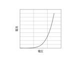
- the current is fixed at a one-to-one ratio with the voltage ( Figure 5), and the voltage and current cannot be adjusted separately.
- the anode 3 can be grounded, making it possible to directly cool the anode 3.
- a floating power supply may be combined in place of the DC power supply 7.
- the outer circumferential surface of the anode 3 as the ground surface, such as the large-diameter cylindrical portion 31 of the anode 3 surrounding the vacuum vessel 10 shown in FIG. 8, or the cathode-side peripheral wall portion 34 provided at one end of the large-diameter cylindrical portion 31 of the anode 3 shown in FIG. 9.
- these configurations make the device configuration more complex and larger, and also increase manufacturing costs.
- the present invention aims to reduce the number of parts in a field emission device and make it smaller.
- one aspect of the field emission device of the present invention includes an insulator joined to a cathode and an anode to form a vacuum vessel, an intermediate electrode joined to the insulator between the cathode and the anode within the vacuum vessel and having a hole through which the electron beam emitted from the cathode to the anode passes, and a conductor protruding from the intermediate electrode, drawn from the insulator along the axial direction of the vacuum vessel, grounded via a DC power source, and connected to the anode.
- the insulator in the field emission device, has a hollow plate portion that seals a central opening and is joined to the cathode and is also joined to the anode.
- the insulator in the field emission device, has a cylinder to one end of which the cathode is joined, and a hollow disk portion provided on the outer periphery of the other end of the cylinder and joined to the anode.
- the anode in the field emission device, has a large-diameter cylindrical portion that is joined to the insulator, and a small-diameter cylindrical portion that communicates with the large-diameter cylindrical portion and contains a target that receives the electron beam.
- one end of the large diameter cylindrical portion is provided with a cathode side peripheral wall portion that extends along the axial direction.
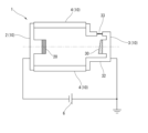
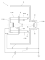
- FIG. 1 is a schematic cross-sectional view of a field emission device including an intermediate electrode according to a first embodiment of the present invention.
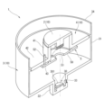
- 1 is a sectional perspective view of a field emission device according to a first embodiment.
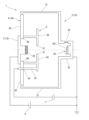
- FIG. 6 is a schematic cross-sectional view of a field emission device according to a second embodiment.
- 1 is a schematic cross-sectional view of a field emission device having a diode structure. The relationship between voltage and current of a diode-type field emission device.
- 1 is a schematic cross-sectional view of a field emission device having a triode structure.
- 1 is a schematic cross-sectional view of a field emission device having a triode structure with an intermediate electrode grounded.
- 1 is a schematic cross-sectional view of a field emission device having a triode structure with the outer circumferential surface being a ground surface.
- 1 is a schematic cross-sectional view of a field emission device having a triode structure with the outer circumferential surface being a ground surface.
- the field emission device 1 of embodiment 1, which is one aspect of the present invention shown in Figure 1, has a cathode 2, an anode 3, an insulator 4, and an intermediate electrode 5.
- the cathode 2 is joined to one end of the insulator 4 coaxially with the anode 3, insulator 4, and intermediate electrode 5, forming a vacuum vessel 10 together with the anode 3 and insulator 4, and is provided with an emitter 20 that emits an electron beam to the target 30 of the anode 3 within this vacuum vessel 10.
- the cathode 2 is grounded via a DC power supply 6 and connected to the anode 3.
- the anode 3 is a cylinder of different diameters coaxial with the cathode 2, insulator 4, and intermediate electrode 5, and has a large-diameter cylindrical portion 31 and a small-diameter cylindrical portion 32 that is connected to the large-diameter cylindrical portion 31 and has a smaller diameter than the large-diameter cylindrical portion 31.
- the inner surface of one end edge of the large-diameter cylindrical portion 31 is joined to the hollow disk portion 42 of the insulator 4.
- the inner surface of the end of the small-diameter cylindrical portion 32 is provided with a target 30 having an inclined surface 301 that receives an electron beam from the emitter 20 and emits X-rays.
- a beam window 33 that emits the X-rays to the outside is provided on the side wall of the small-diameter cylindrical portion 32.
- the anode 3 is connected to a DC power source 6 and is grounded.
- one end of the large-diameter cylindrical portion 31 of the anode 3 along the outer periphery of the hollow disk portion 42 of the insulator 4 is provided with a cathode-side peripheral wall portion 34 that extends along the axial direction of the large-diameter cylindrical portion 31 (vacuum vessel 10).
- the insulator 4 is joined to the cathode 2 and anode 3 to form the vacuum vessel 10.
- the insulator 4 is made of a ceramic member coaxial with the cathode 2, anode 3, and intermediate electrode 5, and has a cylindrical portion 41 to one end of which the cathode 2 is joined, and a hollow plate portion 42 provided on the outer periphery of the other end of the cylindrical portion 41 and joined to the anode 3.
- the hollow plate portion 42 also has an extraction hole 43 formed therein for the conductor 52 of the intermediate electrode 5 from within the vacuum vessel 10.
- the intermediate electrode 5 is joined to the insulator 4 between the cathode 2 and the anode 3 in the vacuum vessel 10 as shown in Figs. 1 and 2, and has a hollow plate portion 50 in which a hole 51 is formed through which the electron beam emitted from the emitter 20 of the cathode 2 to the target 30 of the anode 3 passes. Furthermore, a conductor 52 protrudes from the hollow plate portion 50. The conductor 52 is drawn out along the axial direction of the vacuum vessel 10 from the drawing hole 43 of the hollow plate portion 42 of the insulator 4, and is grounded via the DC power source 7 and connected to the anode 3.
- the cathode 2, anode 3, insulator 4, and intermediate electrode 5 are then vacuum brazed (for example, silver brazing) to seal the cathode 2, anode 3, insulator 4, and intermediate electrode 5, forming the vacuum vessel 10.
- vacuum brazed for example, silver brazing
- the cathode 2, anode 3, insulator 4, and intermediate electrode 5 are assembled and vacuum brazed.
- the conductor 52 of the intermediate electrode 5 and the extraction hole 43 of the insulator 4 are also vacuum brazed.
- the joint of the insulator 4 is metallized to make it easier to braze, but depending on the brazing material used, the joint of the insulator 4 may not need to be metallized.
- the ceramic material area on the cathode 2 side and the ceramic material area on the anode 3 side are integrated, as in the insulator 4, so it is possible to reduce the number of parts in the field emission device 1.
- the configuration of the field emission device 1 is simplified, making it possible to reduce the size of the field emission device 1 and reduce costs.
- the cathode 2 is grounded via the DC power supply 6 and connected to the anode 3, and the conductor 52 is drawn out from the hollow plate portion 42 along the axial direction of the intermediate electrode 5, grounded via the DC power supply 7, and connected to the anode 3, so that the outer periphery of the field emission device 1 becomes the ground surface. Therefore, the advantage of the anode 3 being grounded is utilized, and direct cooling of the anode 3 is also possible.
- cathode side peripheral wall portion 34 which extends from one end of the large diameter cylindrical portion 31 of the anode 3 toward the cathode 2 along the axial direction of the large diameter cylindrical portion 31, allows it to be fitted with surrounding application components, making it easier to incorporate the field emission device 1 into a compact device such as an X-ray source.
- the insulator 4 may not have a cylindrical portion 41 like the insulator 4 of embodiment 2 illustrated in FIG. 3, as long as it is joined to the cathode 2 and anode 3 to form the vacuum vessel 10.
- the insulator 4 in the same figure seals the central opening 40 of the hollow plate portion 42 to be joined to the cathode 2 and also to the anode 3.
- the insulator 4 may also be a cylinder, with the cathode 2 joined to the center of one end surface of the cylinder and the anode 3 joined to the other end surface of the cylinder, and the conductor 52 of the intermediate electrode 5 drawn out from the one end surface.
- Reference Signs List 1...field emission device, 10...vacuum vessel, 2...cathode, 20...emitter, 3...anode, 30...target, 301...inclined surface, 31...large diameter cylinder portion, 32...small diameter cylinder portion, 33...beam window, 34...cathode side peripheral wall portion, 4...insulator, 40...central opening, 41...cylindrical portion, 42...hollow plate portion, 43...drawing hole, 5...intermediate electrode, 50...hollow plate portion, 51...hole, 52...conductor, 6, 7...DC power source
Landscapes
- X-Ray Techniques (AREA)
Abstract
電界放射装置1は、陰極2及び陽極3と接合して真空容器10を成す絶縁体4と、真空容器10内にて陰極2と陽極3との間で絶縁体4に接合され、陰極2から陽極3に放出される電子ビームが通過する孔51が形成された中間極5を有する。中間極5は、絶縁体4から真空容器10の軸方向に沿って引き出されて直流電源7を介して接地されると共に陽極3に接続される導体52を備える。
Description
本発明は冷陰極型の電界放射装置の構造に関する。
X線装置,電子管,照明装置等に適用される図4に示された電界放射装置1は、真空容器10内の陰極2と陽極3との間に電圧を印加し、陰極2のエミッタ20から放出された電子ビームを陽極3のターゲット30に衝突させて所望の機能を発揮する(特許文献1)。例えば、X線装置の場合はX線照射による透視に使用される。
エミッタ20の電子放出は、エミッタ20に印加される電界により決定される。図4に示された2極管構造のX線管の場合、その電流は電圧と1対1で固定され(図5)、電圧と電流を個別に調整できない。
電界放射装置1の電圧と電流の個別の調整は図6に示したように絶縁体4を介して陰極2と陽極3との間に中間極5を配した3極管構造とすれば可能となる(特許文献2)。
X線の発生効率は3%以下と非常に悪く、残りはほぼ熱へと変換される。したがって、ターゲット30を有する陽極3の冷却が課題となる。2極管構造の場合、図4に示したように陽極3を接地とすることでフィンやファンを用いた直接冷却が可能となる。
一方、図6に示した3極管構造の場合、中間極5を接地とすると、陽極3はプラスDC電圧が印加されるので直接冷却が困難となる。
3極管構造は、図7に示された態様のように、エミッタ20に加える電界を、陰極2に接続される直流電源6と中間極5に接続される直流電源7との差分で作り出せば、陽極3を接地とすることができ、陽極3の直接冷却が可能となる。直流電源7のかわりにフローティング電源を組み合わせてもよい。
また、陽極接地となるメリットをより生かすためには、図8に示された真空容器10を包囲する陽極3の大径筒部31や図9に示された陽極3の大径筒部31の一端に設けられる陰極側周壁部34のように陽極3の外周面を接地面とすることが望ましい。しかしながら、これらの態様は装置構成が複雑及び大型化し、また、製造コストも上がる。
本発明は、以上のことを鑑み、電界放射装置の部品点数の削減と小型化を図ることを課題とする。
そこで、本発明の電界放射装置の一態様は、陰極及び陽極と接合して真空容器を成す絶縁体と、前記真空容器内にて前記陰極と前記陽極との間で前記絶縁体に接合され、前記陰極から前記陽極に放出される電子ビームが通過する孔が形成された中間極と、この中間極に突設され、前記絶縁体から前記真空容器の軸方向に沿って引き出されて直流電源を介して接地されると共に前記陽極に接続される導体と、を有する。
本発明の一態様は、前記電界放射装置において、前記絶縁体は、中央開口部を密閉して前記陰極と接合すると共に前記陽極と接合する中空盤部を有する。
本発明の一態様は、前記電界放射装置において、前記絶縁体は、一端に前記陰極が接合する筒体と、この筒体の他端外周に設けられて前記陽極と接合する中空盤部と、を有する。
本発明の一態様は、前記電界放射装置において、前記陽極は、前記絶縁体と接合する大径筒部と、この大径筒部と連通し、前記電子ビームを受けるターゲットを収容する小径筒部と、を有する。
本発明の一態様は、前記電界放射装置において、前記大径筒部の一端には、前記軸方向に沿って延伸する陰極側周壁部が備えられる。
以上の本発明によれば、電界放射装置の部品点数の削減と小型化を図ることができる。
以下に図面を参照しながら本発明の実施形態について説明する。
図1に示された本発明の一態様である実施形態1の電界放射装置1は、陰極2、陽極3、絶縁体4及び中間極5を有する。
陰極2は、陽極3、絶縁体4及び中間極5と同軸に絶縁体4の一端に接合して陽極3及び絶縁体4とで真空容器10を成し、この真空容器10内にて陽極3のターゲット30に電子ビームを放出するエミッタ20を備える。そして、この陰極2は直流電源6を介して接地されると共に陽極3に接続される。
陽極3は、陰極2、絶縁体4及び中間極5と同軸の異径の円筒体を成し、大径筒部31と、この大径筒部31と連通する大径筒部31よりも小径な小径筒部32を有する。大径筒部31の一端縁の内面は、絶縁体4の中空盤部42と接合する。小径筒部32の端部の内面には、エミッタ20から電子ビームを受けてX線を放出する傾斜面301を有するターゲット30が備えられる。また、小径筒部32の側壁部には、前記X線を外部に放出するビーム窓33が設けられる。そして、この陽極3は直流電源6に接続されると共に接地される。
また、絶縁体4の中空盤部42の外周に沿う陽極3の大径筒部31の一端には、大径筒部31(真空容器10)の軸方向に沿って延伸する陰極側周壁部34が備えられる。
絶縁体4は、陰極2及び陽極3と接合して真空容器10を成す。絶縁体4は、陰極2,陽極3及び中間極5と同軸のセラミック部材から成り、一端に陰極2が接合する円筒部41と、この円筒部41の他端外周に設けられて陽極3と接合する中空盤部42を有する。また、中空盤部42には、真空容器10内からの中間極5の導体52の引き出し孔43が形成される。
中間極5は、図1,2に示したように真空容器10内にて陰極2と陽極3との間で絶縁体4に接合され、陰極2のエミッタ20から陽極3のターゲット30に放出される電子ビームが通過する孔51が形成された中空盤部50を備える。さらに、中空盤部50には導体52が突設される。導体52は、絶縁体4の中空盤部42の引き出し孔43から真空容器10の軸方向に沿って引き出され、直流電源7を介して接地される共に陽極3に接続される。
そして、陰極2、陽極3、絶縁体4及び中間極5は、真空ろう付け(例えば銀蝋付け)による接合により封止されて真空容器10が構成される。真空ろう付けにより真空封止する際には陰極2、陽極3、絶縁体4及び中間極5が組み込まれて真空ろう付けされる。中間極5の導体52と絶縁体4の引き出し孔43との間も真空ろう付けされる。絶縁体4の接合部には、メタライズ処理を施してろう付けしやすくしておくが、使用するろう材によっては、絶縁体4の接合部をメタライズ処理しなくてもよい。
以上の電界放射装置1によれば、絶縁体4のように陰極2側のセラミック部材の領域と陽極3側のセラミック部材の領域が一体化しているので、電界放射装置1の部品点数の削減が可能となる。また、電界放射装置1の構成が簡素となり、電界放射装置1の小型化と共にコストの削減も可能となる。
さらに、陰極2が直流電源6を介して接地されると共に陽極3と接続され、また、導体52が中空盤部42から中間極5の軸方向に沿って引き出されて直流電源7を介して接地される共に陽極3に接続されることで、電界放射装置1の外周面が接地面となる。したがって、陽極3が接地となるメリットが生かされ、陽極3の直接冷却も可能となる。
また、陽極3の大径筒部31の一端から陰極2側に大径筒部31の軸方向に沿って延伸する陰極側周壁部34により、周辺の印加部品と嵌合可能となり、電界放射装置1をX線源等の装置にコンパクトに組み込み易くなる。
尚、絶縁体4は、陰極2及び陽極3と接合して真空容器10を成せばよいので、図3に例示された実施形態2の絶縁体4のように円筒部41を備えていなくてもよい。同図の絶縁体4は、中空盤部42の中央開口部40を密閉して陰極2と接合すると共に陽極3と接合する。また、絶縁体4は、筒体を成し、当該筒体の一端面の中央部に陰極2が接合し、当該筒体の他端面に陽極3が接合し、当該一端面から中間極5の導体52が引き出される態様であってもよい。これらの態様によっても上述の実施形態1と同様の効果が得られる。
1…電界放射装置、10…真空容器
2…陰極、20…エミッタ
3…陽極、30…ターゲット、301…傾斜面、31…大径筒部、32…小径筒部、33…ビーム窓、34…陰極側周壁部
4…絶縁体、40…中央開口部、41…円筒部、42…中空盤部、43…引き出し孔
5…中間極、50…中空盤部、51…孔、52…導体
6,7…直流電源
2…陰極、20…エミッタ
3…陽極、30…ターゲット、301…傾斜面、31…大径筒部、32…小径筒部、33…ビーム窓、34…陰極側周壁部
4…絶縁体、40…中央開口部、41…円筒部、42…中空盤部、43…引き出し孔
5…中間極、50…中空盤部、51…孔、52…導体
6,7…直流電源
Claims (5)
- 陰極及び陽極と接合して真空容器を成す絶縁体と、
前記真空容器内にて前記陰極と前記陽極との間で前記絶縁体に接合され、前記陰極から前記陽極に放出される電子ビームが通過する孔が形成された中間極と、
この中間極に突設され、前記絶縁体から前記真空容器の軸方向に沿って引き出されて直流電源を介して接地されると共に前記陽極に接続される導体と、
を有することを特徴とする電界放射装置。 - 前記絶縁体は、中央開口部を密閉して前記陰極と接合すると共に前記陽極と接合する中空盤部を有することを特徴とする請求項1に記載の電界放射装置。
- 前記絶縁体は、
一端に前記陰極が接合する筒体と、
この筒体の他端外周に設けられて前記陽極と接合する中空盤部と、
を有することを特徴とする請求項1に記載の電界放射装置。 - 前記陽極は、
前記絶縁体と接合する大径筒部と、
この大径筒部と連通し、前記電子ビームを受けるターゲットを収容する小径筒部と、
を有することを特徴とする請求項1に記載の電界放射装置。 - 前記大径筒部の一端には、前記軸方向に沿って延伸する陰極側周壁部が備えられたことを特徴とする請求項4に記載の電界放射装置。
Applications Claiming Priority (2)
| Application Number | Priority Date | Filing Date | Title |
|---|---|---|---|
| JP2023-105599 | 2023-06-28 | ||
| JP2023105599A JP7556429B1 (ja) | 2023-06-28 | 2023-06-28 | 電界放射装置 |
Publications (1)
| Publication Number | Publication Date |
|---|---|
| WO2025005128A1 true WO2025005128A1 (ja) | 2025-01-02 |
Family
ID=92839438
Family Applications (1)
| Application Number | Title | Priority Date | Filing Date |
|---|---|---|---|
| PCT/JP2024/023156 Ceased WO2025005128A1 (ja) | 2023-06-28 | 2024-06-26 | 電界放射装置 |
Country Status (2)
| Country | Link |
|---|---|
| JP (1) | JP7556429B1 (ja) |
| WO (1) | WO2025005128A1 (ja) |
Citations (5)
| Publication number | Priority date | Publication date | Assignee | Title |
|---|---|---|---|---|
| JP2004146158A (ja) * | 2002-10-23 | 2004-05-20 | Shigekimi Kita | 電界放出型x線源 |
| JP2009087633A (ja) * | 2007-09-28 | 2009-04-23 | Toshiba Corp | X線源およびx線源の製造方法 |
| JP2012104283A (ja) * | 2010-11-08 | 2012-05-31 | Life Technology Research Institute Inc | 電界放射装置 |
| JP2012252831A (ja) * | 2011-06-01 | 2012-12-20 | Canon Inc | X線管 |
| JP2023011740A (ja) * | 2021-01-06 | 2023-01-24 | キヤノン株式会社 | X線発生管、x線発生装置およびx線撮影システム |
-
2023
- 2023-06-28 JP JP2023105599A patent/JP7556429B1/ja active Active
-
2024
- 2024-06-26 WO PCT/JP2024/023156 patent/WO2025005128A1/ja not_active Ceased
Patent Citations (5)
| Publication number | Priority date | Publication date | Assignee | Title |
|---|---|---|---|---|
| JP2004146158A (ja) * | 2002-10-23 | 2004-05-20 | Shigekimi Kita | 電界放出型x線源 |
| JP2009087633A (ja) * | 2007-09-28 | 2009-04-23 | Toshiba Corp | X線源およびx線源の製造方法 |
| JP2012104283A (ja) * | 2010-11-08 | 2012-05-31 | Life Technology Research Institute Inc | 電界放射装置 |
| JP2012252831A (ja) * | 2011-06-01 | 2012-12-20 | Canon Inc | X線管 |
| JP2023011740A (ja) * | 2021-01-06 | 2023-01-24 | キヤノン株式会社 | X線発生管、x線発生装置およびx線撮影システム |
Also Published As
| Publication number | Publication date |
|---|---|
| JP2025005464A (ja) | 2025-01-17 |
| JP7556429B1 (ja) | 2024-09-26 |
Similar Documents
| Publication | Publication Date | Title |
|---|---|---|
| KR101868009B1 (ko) | 전계 방출 엑스선원 및 이를 이용한 전자 빔 집속 방법 | |
| EP2740332B1 (en) | Radiation generating apparatus and radiation imaging apparatus | |
| US9159525B2 (en) | Radiation generating tube | |
| JP6420444B1 (ja) | 電子集束改善用x線管 | |
| EP2740331B1 (en) | Radiation generating apparatus and radiation imaging apparatus | |
| JP5845342B2 (ja) | X線管およびx線管用電子放出素子 | |
| JP2001504988A (ja) | 低電力xrf応用のための、空冷式で端部に窓を有する金属―セラミック製x線管 | |
| US10832884B2 (en) | Cylindrical X-ray tube and manufacturing method thereof | |
| US8675818B2 (en) | Ceramic metallization in an x-ray tube | |
| JP2019186095A (ja) | X線管 | |
| JP6792676B1 (ja) | X線管 | |
| JP7556429B1 (ja) | 電界放射装置 | |
| JP4967854B2 (ja) | X線管装置 | |
| US8867706B2 (en) | Asymmetric x-ray tube | |
| CN216015285U (zh) | 一种全角度的弧形阵列x射线管及环形射线装置 | |
| JP2007042434A (ja) | X線管 | |
| US20260081090A1 (en) | Multi-directional connection hub and cold cathode x-ray tube that can easily change its characteristics and its connection method | |
| AU763548B2 (en) | High energy X-ray tube | |
| KR20250162648A (ko) | 엑스레이소스 | |
| KR20260040930A (ko) | 다방향 연결 허브 및 이에 의해 특성 변경이 용이한 냉음극 엑스선 튜브와 그 연결방법 | |
| JPH03283243A (ja) | X線発生装置 |
Legal Events
| Date | Code | Title | Description |
|---|---|---|---|
| 121 | Ep: the epo has been informed by wipo that ep was designated in this application |
Ref document number: 24831987 Country of ref document: EP Kind code of ref document: A1 |
|
| NENP | Non-entry into the national phase |
Ref country code: DE |