WO2025005116A1 - 光学シート - Google Patents
光学シート Download PDFInfo
- Publication number
- WO2025005116A1 WO2025005116A1 PCT/JP2024/023130 JP2024023130W WO2025005116A1 WO 2025005116 A1 WO2025005116 A1 WO 2025005116A1 JP 2024023130 W JP2024023130 W JP 2024023130W WO 2025005116 A1 WO2025005116 A1 WO 2025005116A1
- Authority
- WO
- WIPO (PCT)
- Prior art keywords
- light
- optical sheet
- layer
- base
- optical
- Prior art date
- Legal status (The legal status is an assumption and is not a legal conclusion. Google has not performed a legal analysis and makes no representation as to the accuracy of the status listed.)
- Ceased
Links
Images


Classifications
-
- G—PHYSICS
- G02—OPTICS
- G02B—OPTICAL ELEMENTS, SYSTEMS OR APPARATUS
- G02B5/00—Optical elements other than lenses
Definitions
- the present invention relates to an optical sheet that controls the exit direction of incident light.
- Patent Documents 1 and 2 disclose optical films that are less susceptible to problems caused by warping and optical adhesion.
- the present invention aims to provide an optical sheet that has layers in which light-transmitting sections and light-absorbing sections are arranged alternately, has flexibility in the layer configuration, and can suppress warping.
- the present application discloses an optical sheet having a base layer and an optical functional layer laminated on the base layer and in which light-transmitting sections and light-absorbing sections are arranged alternately, in which the optical functional layer has light-transmitting sections that have a predetermined cross section and extend in one direction, and a plurality of light-absorbing sections are arranged at intervals in a direction different from the one direction, and the light-transmitting sections are arranged between the light-transmitting sections, and in which, when the indentation hardness of the light-absorbing sections at position Mb on the base layer side is Hb and the indentation hardness of the light-absorbing sections at position Ma on the opposite side to the base layer is Ha , H a > H b .
- H a >H c >H b may be satisfied.
- the configuration may be such that ⁇ (H a +H b )/2 ⁇ >H c holds.
- (H b /H a ) ⁇ 100% may be set to be equal to or greater than 70% and equal to or less than 85%.
- H a may be set to be equal to or greater than 212 MPa and equal to or less than 271 MPa.
- the substrate layer may be made of polycarbonate resin.
- the light-transmitting portion may have a trapezoidal cross section with a long lower base on the side of the base layer and a short upper base on the opposite side.
- the light absorbing portion may have a trapezoidal cross section with a long bottom base on the upper side of the light transmitting portion and a short top base on the opposite side.
- the light absorbing portion may be configured so that transparent resin contains light absorbing particles made of carbon black.
- the occurrence of warping can be suppressed by adjusting the indentation hardness of the light-absorbing sections, thereby increasing the degree of freedom in the layer configuration that constitutes the optical sheet.
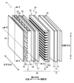
- FIG. 2 is an exploded perspective view illustrating the image source unit 10.
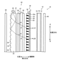
- 2 is an exploded view showing a cross section of the image source unit 10.
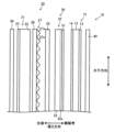
- FIG. 2 is an exploded view showing another cross section of the image source unit 10.
- FIG. 2 is an enlarged view focusing on the optical sheet 30.
- FIG. 1 is a diagram illustrating indentation hardness.
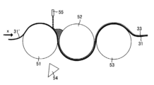
- 3A to 3C are diagrams illustrating a manufacturing process of the optical sheet 30.
- 3A to 3C are diagrams illustrating a manufacturing process of the optical sheet 30.
- Image source unit Fig. 1 is a diagram for explaining one embodiment, and is an exploded perspective view of an image source unit 10 including an optical sheet 30.
- Fig. 2 shows a part of an exploded cross-sectional view of the image source unit 10 cut along the line II-II (vertical line) shown in Fig. 1
- Fig. 3 shows a part of an exploded cross-sectional view of the image source unit 10 cut along the line III-III (horizontal line).
- an image source unit 10 is housed in a housing (not shown) together with normal equipment required for operating the image source unit 10, such as a power source for operating the image source unit 10 and an electronic circuit for controlling the image source unit 10, to form a display device.
- a liquid crystal image source unit will be described as one embodiment of the image source unit
- a liquid crystal display device will be described as one embodiment of the display device.
- the image source unit 10 will be described below.
- the image source unit 10 includes a liquid crystal panel 15, a surface light source device 20, and a functional film 40.
- the optical sheet 30 is included in the surface light source device 20.
- Figures 1 to 3 also show the orientation of the display device when it is installed.
- the liquid crystal panel 15 has an upper polarizing plate 13 arranged on the viewer side, a lower polarizing plate 14 arranged on the surface light source device 20 side, and a liquid crystal layer 12 arranged between the upper polarizing plate 13 and the lower polarizing plate 14.
- the upper polarizing plate 13 and the lower polarizing plate 14 have the function of decomposing incident light into two orthogonal polarized components (P waves and S waves), transmitting the polarized component in one direction (parallel to the transmission axis) (e.g., P waves) and absorbing the polarized component in the other direction (parallel to the absorption axis) orthogonal to the one direction (e.g., S waves).
- the liquid crystal layer 12 has multiple pixels arranged vertically and horizontally along the layer surface, and an electric field can be applied to each region that forms one pixel.
- the orientation of the pixel to which the electric field is applied changes.
- the polarized component e.g. P wave
- the polarized component parallel to the transmission axis that has passed through the lower polarizer 14 arranged on the surface light source device 20 side (i.e. the light input side) rotates its polarization direction by 90° when passing through a pixel to which an electric field is applied, while maintaining its polarization direction when passing through a pixel to which no electric field is applied. Therefore, depending on whether or not an electric field is applied to the pixel, it is possible to control whether the polarized component (e.g. P wave) that has passed through the lower polarizer 14 is further transmitted through the upper polarizer 13 arranged on the light output side, or is absorbed and blocked by the upper polarizer 13.
- the liquid crystal panel 15 has a structure that controls the transmission or blocking of light from the surface light source device 20 for each pixel to display images.
- liquid crystal panels there are several types of liquid crystal panels, but in this embodiment, the type is not particularly limited, and any known type of liquid crystal panel can be used. Specific examples include TN, STN, VA, MVA, IPS, OCB, etc.
- the surface light source device 20 is an illumination device that is disposed on the opposite side of the liquid crystal panel 15 from the observer side, and emits planar light toward the liquid crystal panel 15.
- the surface light source device 20 of this embodiment is configured as an edge-light type surface light source device, and includes a light guide plate 21, a light source 25, a light diffusion plate 26, a prism layer 27, a reflective polarizing plate 28, an optical sheet 30, and a reflective sheet 39.
- the light guide plate 21 has a base 22 and rear surface optical elements 23.
- the light guide plate 21 is a plate-shaped member made of a light-transmitting material.
- one plate surface side of the light guide plate 21 facing the observer is a smooth surface, and the other plate surface side opposite to this is a rear surface, on which a plurality of rear surface optical elements 23 are arranged.
- thermoplastic resins such as polymer resins with alicyclic structures, methacrylic resins, polycarbonate resins, polystyrene resins, acrylonitrile-styrene copolymers, methyl methacrylate-styrene copolymers, ABS resins, and polyethersulfones, as well as epoxy acrylate and urethane acrylate reactive resins (ionizing radiation curable resins, etc.).
- the base 22 is a plate-like portion with a predetermined thickness through which light is guided and which serves as the base for the rear optical element 23.
- the rear surface optical element 23 is a protruding element formed on the rear surface side of the base 22, and in this embodiment, is a triangular prism.
- the rear surface optical element 23 is a prism with a ridgeline of the protruding apex extending in the horizontal direction, and a plurality of rear surface optical elements 23 are arranged at a predetermined pitch in a direction perpendicular to the extending direction (vertical direction).
- the rear surface optical element 23 in this embodiment has a triangular cross section, but is not limited thereto, and may have any cross section such as a polygonal, hemispherical, part of a sphere, or lens shape.
- the arrangement direction of the multiple rear optical elements 23 is preferably the light guide direction.
- the rear optical elements 23 are arranged in a direction away from the light source 25, and the ridges of the rear optical elements 23 extend parallel to the arrangement direction of the light source 25 or, in the case of a single long light source, the extension direction of the light source.
- triangular shape does not only mean a triangular shape in the strict sense, but also includes an approximate triangular shape that takes into account limitations in manufacturing technology and molding errors.
- terms used in this specification that specify other shapes and geometric conditions, such as “parallel,” “orthogonal,” “ellipse,” and “circle,” are also to be interpreted without being bound by their strict meaning, but with an allowance for errors that may be expected to provide similar optical functions.
- the light guide plate 21 having such a configuration can be manufactured by extrusion molding, or by molding the rear optical elements 23 on the base 22.
- the base 22 and the rear optical elements 23 can be integrally formed.
- the rear optical elements 23 may be made of the same resin material as the base 22, or a different material.
- the light source 25 is disposed on one of the side surfaces (end surfaces) of the base 22 of the light guide plate 21 in the direction in which the rear surface optical elements 23 are arranged.
- the type of light source is not particularly limited, and may be configured in various forms such as a fluorescent lamp such as a linear cold cathode fluorescent tube, a point-shaped LED (light emitting diode), or an incandescent light bulb.
- the light source 25 is configured to be composed of a plurality of LEDs, and is configured so that the turning on and off of each LED and/or the brightness of each LED when turned on can be individually and independently adjusted by a control device (not shown).
- the light source 25 is disposed on one side surface (end surface) as described above, but a light source may also be disposed on the side surface (end surface) opposite to the side surface (end surface).
- the shape of the rear surface optical element is also formed following a known example.
- the light diffusion plate 26 is a layer disposed on the light output side of the light guide plate 21 and has the function of diffusing and outputting the light incident thereon. This can further increase the uniformity of the light output from the light guide plate 21 and make scratches on the light guide plate 21 less noticeable.
- a known light diffusion plate can be used, and for example, a form in which a light diffusion agent is dispersed in a base material can be mentioned.
- the light diffusion plate 26 can be used as a support plate for the prism layer 27.
- the light diffusion plate 26 may be bonded to the light guide plate 21 to be integrated with it.
- the prism layer 27 is provided closer to the liquid crystal panel 15 than the light diffusion plate 26, and is a layer including unit prisms 27a that are convex toward the liquid crystal panel 15.
- the unit prisms 27a have a predetermined cross section and extend in the light guide direction of the light guide plate 21 (vertical direction in this embodiment).
- the multiple unit prisms 27a are arranged in a direction different from the light guide direction (horizontal direction, a direction perpendicular to the light guide direction in a plan view in this embodiment).
- the cross-sectional shape of the unit prism of such a prism layer can be any known shape depending on the required function. Depending on the shape, the light can be further diffused or concentrated.
- the direction in which the unit prisms extend and the direction in which they are arranged are not limited to the above and may be other directions.
- the unit prism may have a predetermined cross section and extend in a direction perpendicular to the light guiding direction of the light guiding plate 21, and a plurality of unit prisms may be arranged in the light guiding direction.
- Reflective polarizing plate 28 has a function of decomposing the incident light into two orthogonal polarized components (P wave and S wave), transmitting the polarized component in one direction (parallel to the transmission axis) (e.g., P wave) and reflecting the polarized component in the other direction (parallel to the reflection axis) orthogonal to the one direction (e.g., S wave).
- P wave and S wave orthogonal polarized components
- Fig. 4 shows an enlarged view of a portion of the optical sheet 30 seen from the perspective of Fig. 2.
- the optical sheet 30 includes a base layer 31 formed in a sheet shape, and an optical function layer 32 provided on one surface of the base layer 31 (the surface on the light guide plate 21 side in this embodiment).
- the base layer 31 is a flat sheet-like member that supports the optical function layer 32 .
- Various materials can be used as the material for the base layer 31.
- materials that are widely used as materials for optical sheets incorporated in display devices, have excellent mechanical properties, optical properties, stability, and processability, and are inexpensively available can be used.
- transparent resin films, transparent resin plates, transparent resin sheets, and transparent glass can be used.
- polyester films such as triacetate cellulose (TAC) films, polyethylene terephthalate (PET), diacetyl cellulose films, acetate butyrate cellulose films, polyethersulfone films, polyacrylic resin films, polyurethane resin films, polyester films, polycarbonate films, polysulfone films, polyether films, polymethylpentene films, polyether ketone films, and (meth)acrylonitrile films can be suitably used, and among these, polyester films are preferably used.
- polyester films in addition to polyethylene terephthalate, polybutylene terephthalate, polynaphthalene terephthalate, polytrimethylene terephthalate, and the like can be used.
- polycarbonate resins with a high glass transition point are desirable.
- the glass transition point of polycarbonate resin is 143° C., which is generally suitable for in-vehicle applications requiring durability at 105° C.
- the optical function layer 32 is a layer laminated on one surface of the base layer 31 (the surface on the light guide plate 21 side in this embodiment), and is configured to have light-transmitting portions 33 and light-absorbing portions 34.
- the optical function layer 32 has a shape that has the cross section shown in Figures 2 and 4 and extends toward the back/front of the page (the horizontal direction when the image source unit 10 is viewed from the front), and the light-transmitting portions 33 and light-absorbing portions 34 are alternately arranged along the layer surface in a direction different from the extending direction (the vertical direction in this embodiment).
- the light-transmitting section 33 is a section whose main function is to transmit light, and in this embodiment, in the cross sections shown in Figures 2 and 4, it is an element having a generally trapezoidal cross-sectional shape with a long lower base on the base layer 31 side and a short upper base on the opposite side (the light guide plate 21 side).
- the light transmitting portions 33 extend in one direction (horizontal direction in this embodiment) while maintaining the cross section along the layer surface of the base material layer 31, and are arranged at a predetermined interval in a direction different from the extending direction (vertical direction in this embodiment).
- a gap (groove) having a substantially trapezoidal cross section is formed between adjacent light transmitting portions 33.
- the gap has a trapezoidal cross section with a long bottom base on the top bottom side (light guide plate 21 side) of the light transmitting portion 33 and a short top base on the bottom bottom side (base material layer 31 side) of the light transmitting portion 33, and the light absorbing portion 34 is formed by filling this with a necessary material described later.
- a plurality of light transmitting portions 33 are connected on their lower bottom sides (base layer side 31) by a sheet-like base portion 32a.
- the light transmitting portion 33 has a refractive index of Nt .
- a light transmitting portion 33 can be formed by curing a light transmitting portion-constituting composition.
- the value of the refractive index Nt is not particularly limited, but from the viewpoint of appropriately reflecting light (including total reflection) at the interface with the light absorbing portion 34 at the inclined surface of the trapezoidal cross section as described below, the refractive index is preferably 1.47 or more. However, since materials with too high a refractive index are often prone to cracking, the refractive index is preferably 1.61 or less. More preferably, it is 1.49 or more and 1.56 or less, and even more preferably 1.56.
- the light absorbing section 34 functions as a gap formed by filling the above-mentioned gap (groove) between adjacent light transmitting sections 33 with a material, and has a basic structure with a cross-sectional shape similar to the cross-sectional shape of the gap. Therefore, in this embodiment, the short upper base faces the liquid crystal panel 15 side (base material layer 31 side), and the long lower base faces the light guide plate 21 side.
- the light absorbing section 34 has a refractive index of Nr and is configured to absorb light. Specifically, light absorbing particles are dispersed in a transparent resin having a refractive index of Nr .
- the refractive index Nr is a refractive index lower than the refractive index Nt of the light transmitting section 33.
- the refractive index of the light absorbing section 34 is not particularly limited, and is preferably 1.47 or more on the premise that the total reflection can be performed appropriately. However, since materials with too high a refractive index are often prone to cracking, the refractive index is preferably 1.61 or less. More preferably, the refractive index is 1.49 or more and 1.56 or less, and even more preferably 1.49.
- the difference in refractive index between the refractive index Nt of the light transmitting portion 33 and the refractive index Nr of the light absorbing portion 34 is not particularly limited, but is preferably greater than 0 and equal to or less than 0.14, and more preferably greater than or equal to 0.05 and equal to or less than 0.14. By increasing the difference in refractive index, more light can be totally reflected.
- the light absorbing portion 34 has interfaces 34a and 34b with the light transmitting portion 33, and the interface angle of the interface 34a is shown as ⁇ 11 in FIG. 4, and the interface angle of the interface 34b is shown as ⁇ 12 in FIG. 4, which are angles formed with the normal line of the layer surface of the optical function layer 32.
- the angles are not particularly limited, but are preferably 0° or more and 10° or less. This makes it possible to increase the brightness in the front direction.
- ⁇ 11 and ⁇ 12 are 0°, the cross sections of the light transmitting portion and the light absorbing portion are rectangular.
- the angles ⁇ 11 and ⁇ 12 may be the same or different.
- the pitch of the light transmitting portion 33 and the light absorbing portion 34 is preferably 20 ⁇ m or more and 100 ⁇ m or less, and more preferably 30 ⁇ m or more and 100 ⁇ m or less.
- the thickness of the light absorbing portion 34, indicated by D in Fig. 4 is preferably 50 ⁇ m or more and 150 ⁇ m or less, and more preferably 60 ⁇ m or more and 150 ⁇ m or less. By setting it within these ranges, it is possible to achieve a more appropriate balance between light transmission and light absorption.
- the light absorption in the light absorbing section 34 can be adjusted by the content ratio of the light absorbing particles in the light absorbing section 34.
- the content ratio of the light absorbing particles to the entire composition (transparent resin + light absorbing particles) constituting the light absorbing section is preferably greater than 10% by mass and less than or equal to 30% by mass. If the content ratio is less than 10% by mass, there is a risk that the light absorbing performance (light blocking properties) of the light absorbing section will be insufficient, and if the content ratio is greater than 30% by mass, there is a risk that the curing property of the light absorbing section will be insufficient, increasing the possibility of problems such as the light absorbing particles falling off.
- the interfaces 34a, 34b between the light transmitting portion 33 and the light absorbing portion 34 are linear in cross section, but the present invention is not limited to this and may be polygonal, convex curved, concave curved, etc.
- the cross-sectional shapes of the multiple light transmitting portions 33 and light absorbing portions 34 may be the same, or may be different cross-sectional shapes with a predetermined regularity.
- the light absorbing portion 34 further has the following characteristics.
- An explanatory diagram is shown in Fig. 5.
- Fig. 5 is a cross section of one light absorbing portion 34, and is a cross section from the same viewpoint as Fig. 4 (a cross section perpendicular to the extension direction of the light absorbing portion 24).
- the light absorbing portion 34 has an indentation hardness H a at a position M a in the cross section, which is greater than an indentation hardness H b at a position M b , that is, H a >H b .
- the indentation hardness Hc at position M c which is located between positions M a and M b
- the indentation hardness is also between H a and H b . That is, it is preferable that H a > H c > H b .
- H c may be smaller than the average value of H a and H b . That is, it is possible to have H a > H b and ⁇ (H a + H b )/2 ⁇ > H c .
- the ratio represented by (H b /H a ) ⁇ 100(%) is 70% or more and 85% or less.
- the ratio represented by (H b /H a ) ⁇ 100(%) is 70% or more and 85% or less, in addition to suppressing warpage, the following effect is achieved.
- An optical sheet having an optical functional layer in which light transmitting portions and light absorbing portions are alternately arranged on a base layer as in the present disclosure can be stored in a rolled state (a state in which a long strip-shaped sheet before being cut into the size of the optical sheet is rolled up) after the light absorbing portions are formed.
- the light transmitting portion has a trapezoidal cross section with a long lower base on the base layer side and a short upper base on the opposite side
- the light absorbing portion has a trapezoidal cross section with a short upper base on the base layer side ( Mb side, Hb side)
- the light absorbing portion on the Mb ( Hb ) side is required to have appropriate flexibility against the stress caused by the roll due to the short upper base.
- the light absorbing portion with the short upper base on the Mb ( Hb ) side is required to have appropriate indentation hardness characteristics.
- Hb satisfies the ratio represented by ( Hb / Ha ) x 100(%) of 70% or more and 85% or less, or, as described below, is 145 MPa or more and 177 MPa or less.
- the magnitude of the indentation hardness H a is not particularly limited, but is preferably 212 MPa or more and 271 MPa or less. This makes it possible to more reliably suppress the occurrence of warping of the optical sheet.
- the magnitude of the indentation hardness H a is more preferably 212 MPa or more and 254 MPa or less.
- the magnitude of the indentation hardness Hb may be any value as long as it satisfies the above-mentioned relationship, and Hb is preferably 145 MPa or more and 177 MPa or less, and more preferably 160 MPa or more and 177 MPa or less.
- the magnitude of the indentation hardness Hc may also satisfy the above-mentioned relationship, and Hc is preferably 149 MPa or more and 213 MPa or less, and more preferably 162 MPa or more and 213 MPa or less.
- the combination of the indentation hardness H a and the indentation hardness H b may be H a >H b , and it is particularly preferable that H a is 158 MPa or more and 271 MPa or less, and H b is 145 MPa or more and 177 MPa or less.
- the positions M a , M b , and M c are defined as follows.
- the center of the bottom (shorter upper base) of the light absorbing portion 34 on the base material layer 31 side is C1
- the center of the bottom (longer lower base) of the light absorbing portion 34 on the opposite side to the base material layer 31 is C2
- the line connecting C1 and C2 is C
- positions M a , M b , and M c are all on line C.
- the centers C 1 and C 2 are considered to be a straight line connecting the ends of the bottom.
- M a is located at a distance of 0.1L A from C 2
- M b is located at a distance of 0.1L A from C 1.
- M c is located in the middle between M a and M b .
- light absorbing particles are present at the positions Ma , Mb , and Mc , the positions closest to the positions except for the light absorbing particles are used.
- the indentation hardness specified in ISO14577-1 is measured in accordance with ISO14577-1 2002-10-01 Part 1, and can be measured, for example, using an ultra-microindentation hardness tester (nanoindentation tester) ENT1100a manufactured by Elionix Co., Ltd., with an indentation load of 10 mgf (divided into 250 steps) and a test load holding time of 1 second.
- an ultra-microindentation hardness tester nanoindentation tester
- ENT1100a manufactured by Elionix Co., Ltd.
- optical sheet manufacturing method The optical sheet 30 as described above can be produced, for example, as follows.
- the light transmitting portion 33 is formed on one surface of the substrate layer 31.
- the substrate sheet 31' to be the substrate layer 31 is inserted between the mold roll 52 having a shape on its surface that can transfer the shape of the light transmitting portion 33 and the nip roll 51 arranged to face it.
- a predetermined gap is provided between the mold roll 52 and the nip roll 51 to form the base portion 32a.
- the mold roll 52 and the nip roll 51 are rotated while supplying the composition constituting the light transmitting portion between the substrate sheet 31' and the mold roll 52 from the supply device 55.
- the composition constituting the light transmitting portion is filled into the grooves (the shape of the unit light transmitting element inverted) corresponding to the unit light transmitting elements formed on the surface of the mold roll 52, and the composition conforms to the surface shape of the mold roll 52.
- the composition constituting the light transmitting portion include ionizing radiation curable resins such as epoxy acrylates, urethane acrylates, polyether acrylates, polyester acrylates, and polythiols.
- the composition that constitutes the light-transmitting portion which is sandwiched between the mold roll 52 and the base sheet 31' and filled therein, is irradiated with light from the base sheet side by the light irradiation device 54 for hardening. This hardens the composition and fixes its shape. Then, the base layer 31 and the molded light-transmitting portion 33 are released from the mold roll 52 by the release roll 53.
- the light absorbing portions 34 are formed.
- the gaps (grooves) between the light transmitting portions 33 formed above are filled with the ink composition 57 that constitutes the light absorbing portions.
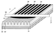
- excess composition is scraped off with a doctor blade 58 or the like.
- the remaining ink composition is cured by irradiating it with ultraviolet light from the unit light transmitting element 33 side, thereby forming the light absorbing portions 34.
- this can be performed, for example, as follows.
- the grooves 33' between the parallel light-transmitting portions 33 are filled with an ink composition 57 containing a transparent ionizing radiation resin composition and light-absorbing particles.
- the ink composition 57 can be filled into the wedge-shaped grooves by, for example, dropping with a dispenser, applying with a die head, or using a finisher roll.
- the ink composition contains a transparent ionizing radiation curable resin composition and light absorbing particles as components.
- a transparent ionizing radiation curable resin composition a conventionally known ionizing radiation curable resin composition used in a visibility improving sheet, a viewing angle improving sheet, etc. can be used.
- a resin having an acrylate-based functional group can be suitably used, and specific examples thereof include oligomers or prepolymers such as (meth)acrylates of polyfunctional compounds such as relatively low molecular weight polyester resins, polyether resins, acrylic resins, epoxy resins, urethane resins, alkyd resins, spiroacetal resins, polybutadiene resins, polythiolpolyene resins, and polyhydric alcohols.
- a reactive diluent may be added to the resin composition.
- a monofunctional monomer or a polyfunctional monomer such as ethyl (meth)acrylate, ethylhexyl (meth)acrylate, styrene, methylstyrene, or N-vinylpyrrolidone may be used.
- the reactive diluent include trimethylolpropane tri(meth)acrylate, hexanediol (meth)acrylate, tripropylene glycol di(meth)acrylate, diethylene glycol di(meth)acrylate, pentaerythritol tri(meth)acrylate, dipentaerythritol hexa(meth)acrylate, 1,6-hexanediol di(meth)acrylate, and neopentyl glycol di(meth)acrylate.
- acetophenones, benzophenones, Michler's benzoyl benzoate, ⁇ -amyloxime ester, tetramethylthiuram monosulfide, thioxanthones, etc. as photopolymerization initiators, or n-butylamine, triethylamine, poly-n-butylphosphine, etc. as photosensitizers can be mixed into the composition.
- resin beads or glass beads may be used, and colored particles capable of selectively absorbing a specific wavelength in accordance with the characteristics of the image light may be used.
- Colorants such as carbon black, graphite, fibrous carbon, metal salts such as black iron oxide, dyes, pigments, etc. may be kneaded into the resin beads or glass beads. From the viewpoint of ease of kneading the colorant, it is preferable to use resin beads.
- resin beads melamine beads, acrylic beads, acrylic-styrene beads, polycarbonate beads, polyethylene beads, polystyrene beads, PVC beads, etc. can be suitably used.
- urethane crosslinked fine particles and silicon-based beads can also be suitably used.
- the resin before kneading the colorant a transparent resin can be used, but it is preferable to use a resin colored with a pigment or dye, etc., and it may be a resin that selectively absorbs a specific wavelength in accordance with the characteristics of the image light, but preferably resin beads colored black are used.
- the average particle diameter of the light absorbing particles is preferably 1.0 ⁇ m or more and 20 ⁇ m or less, more preferably 1.0 ⁇ m or more and 10 ⁇ m or less, and even more preferably 1.0 ⁇ m or more and 4.0 ⁇ m or less.
- average particle diameter refers to the diameter obtained by observing 100 light absorbing particles with an electron microscope, measuring their diameters, and arithmetically averaging them.
- carbon black can be preferably used among the above-mentioned.
- the amount of carbon black kneaded into the resin beads is about 0.1 to 0.7 parts by mass, preferably 0.15 to 0.5 parts by mass, and more preferably 0.2 to 0.35 parts by mass, per 1 part by mass of the resin beads. If the amount of carbon black kneaded is more than 0.7 parts by mass, the resin beads may be easily broken, while if it is less than 0.1 parts by mass, fine particles having the desired blackness may not be obtained.
- carbon black having an average particle size of 10 to 500 nm can be preferably used, and for example, furnace black, acetylene black, channel black, thermal black, carbon nanotube, carbon fiber, etc. can be used.
- the average particle size here means the arithmetic mean diameter determined by observing carbon black particles under an electron microscope.
- the particles may be surface-treated in advance, for example, by a conventionally known hydrophilic treatment using silica coating or surface modification using plasma or the like.
- the ink composition containing the above-mentioned components is prepared by mixing a predetermined amount of light-absorbing particles with an ionizing radiation curable resin composition, and adding a polymerization initiator, etc., if desired.
- the amount of colored fine particles added is preferably in the range of 15 to 35% of the total mass of the ink composition, and by setting it in this range, a visibility improving sheet with better contrast can be realized. If the content of the light-absorbing particles is too small, the light blocking ability of the light-absorbing part may be insufficient, and if the content of the light-absorbing particles is too large, the resin beads come into contact with each other, easily causing problems such as cracking and chipping.
- the excess ink composition 57 is scraped off with a doctor blade 58 as shown in FIG. 7 so that the ink composition 57 fills the grooves 33'.
- the ink composition 57 is scraped off by the doctor blade 58 by pressing the doctor blade 58 against the light-transmitting portion 33 with a predetermined pressure (pressing force) while moving the laminate of the base layer 31 and the light-transmitting portion 33 at a predetermined speed V.
- the curing method can be by irradiation with electron beams or ultraviolet rays.
- electron beam curing an electron beam having an energy of 50 to 1000 keV, preferably 100 to 300 keV, emitted from various electron beam accelerators such as Cockcroft-Walton type, Van de Graaff type, resonant transformer type, insulating core transformer type, linear type, dynamitron type, and high frequency type, etc.
- ultraviolet ray curing ultraviolet emitted from light beams of ultra-high pressure mercury lamps, high pressure mercury lamps, low pressure mercury lamps, carbon arcs, xenon arcs, metal halide lamps, etc. can be used.
- the dose of the electron beam or ultraviolet light to be irradiated can be reduced and the
- the reflective sheet 39 of the surface light source device 20 will be described.
- the reflective sheet 39 is a member for reflecting light emitted from the rear surface of the light guide plate 21 and causing the light to enter the light guide plate 21 again.
- a sheet capable of so-called specular reflection such as a sheet made of a material having a high reflectance such as a metal, or a sheet including a thin film (e.g., a metal thin film) made of a material having a high reflectance as a surface layer, can be preferably used.
- the functional film 40 is disposed on the light output side of the liquid crystal panel 15, and is a layer having the function of improving the quality of the image light and protecting the image source unit 10.
- a layer include an anti-reflection film, an anti-glare film, a hard coat film, a color correction film, and a light diffusion film, and these may be used alone or in combination.
- optical sheet 30 having the above-mentioned configuration
- the examples of optical paths are conceptual examples for the purpose of explanation, and do not strictly represent the degree of reflection or refraction.
- FIG. 2 shows, as an example, an example of the optical path of light L21, L22 entering the light guide plate 21 from the light source 25.
- the light L21 and L22 incident on the light guide plate 21 are repeatedly totally reflected on the light-emitting side of the light guide plate 21 and on the back surface on the opposite side due to the difference in refractive index with air, and proceed in the light guide direction (downward in the plane of the paper in FIG. 2).
- a rear optical element 23 is disposed on the rear surface of the light guide plate 21. Therefore, as shown in FIG. 2, the direction of light L21, L22 traveling inside the light guide plate 21 may change due to the rear optical element 23, and may be incident on the light output surface and rear surface at an angle of incidence less than the critical angle of total reflection. In this case, the light may be emitted from the light output surface of the light guide plate 21 and the rear surface on the opposite side.
- the light L21 and L22 emitted from the light output surface travels toward the light diffusion plate 26 arranged on the light output side of the light guide plate 21.
- the light emitted from the rear surface is reflected by the reflective sheet 39 arranged on the rear surface of the light guide plate 21, and enters the light guide plate 21 again to travel within the light guide plate 21.
- the light traveling through the light guide plate 21 and the light that is redirected by the rear optical element 23 and reaches the light output surface at an angle of incidence less than the critical angle of total reflection are generated in each area along the light guide direction within the light guide plate 21.
- the light traveling through the light guide plate 21 is gradually emitted from the light output surface. This makes it possible to uniformize the light amount distribution along the light guide direction of the light that is emitted from the light output surface of the light guide plate 21.
- the light emitted from the light guide plate 21 then reaches the light diffusion plate 26, where the uniformity is increased.
- the light is then diffused or concentrated as necessary by the prism layer 27, and the light that has exited the prism layer 27 reaches the reflective polarizing plate 28.
- the light polarized in the direction along the transmission axis of the reflective polarizing plate 28 passes through the reflective polarizing plate 28 and travels toward the optical sheet 30.
- light polarized in the direction along the reflection axis of reflective polarizer 28 is reflected as shown by the dotted arrow in Fig. 2 and returned to the light guide plate 21 side.
- the returned light is reflected by the light guide plate 21, rear optical element 23, or reflective sheet 39 and travels again toward the reflective polarizer 28 side.
- the polarization direction of some of the light changes, and some of this light passes through reflective polarizer 28.
- the other light is returned again to the light guide plate side.
- the light reflected by reflective polarizer 28 can also pass through reflective polarizer 28 by repeating reflections. This increases the utilization rate of light from light source 25.
- the polarization direction of the light emitted from the reflective polarizing plate 28 is aligned along the transmission axis of the lower polarizing plate 14 , and the light becomes polarized light that passes through the lower polarizing plate 14 .
- the light that leaves the reflective polarizing plate 28 reaches the optical sheet 30.
- the light that enters the optical sheet 30 travels along the following optical path.
- An example of the optical path in the optical sheet 30 is shown in Figure 4.
- the light travels toward the interface between the light transmitting portions 33 and the light absorbing portions 34, as with the light L21 and light L22 shown in Fig. 2 and the light L41 and light L42 shown in Fig. 4. Then, the light is totally reflected at the interface, and the light is controlled to travel in a desired direction so that the viewing angle is limited. If necessary, the angle of the interface between the light-transmitting portion 33 and the light-absorbing portion 34 ( ⁇ 11 , ⁇ 12 in FIG. 4 ) can be adjusted to direct the light in a direction having a desired angle with respect to the normal direction of the optical sheet (i.e., the front direction).
- L43 shown in FIG. 4 travels at an angle that transmits through the interface between the light transmitting portion 33 and the light absorbing portion 34 without being totally reflected at the interface, and is therefore transmitted through the interface and absorbed by the light absorbing portion 34.
- This makes it possible to efficiently absorb and block light that is emitted at a viewing angle of a predetermined angle or more, thereby limiting the viewing angle.
- since such light is highly likely to enter the liquid crystal panel and cause problems such as reduced contrast and color inversion, it is possible to absorb such light.
- the light that exits the optical sheet 30 is incident on the lower polarizer 14 of the liquid crystal panel 15.
- the lower polarizer 14 transmits one polarized component of the incident light and absorbs the other polarized component.
- the light that passes through the lower polarizer 14 selectively passes through the upper polarizer 13 depending on the state of the electric field applied to each pixel.
- the liquid crystal panel 15 selectively transmits the light from the surface light source device 20 for each pixel, allowing the viewer of the liquid crystal display device to view an image. At that time, the image light is provided to the viewer via the functional film 40, improving the quality of the image.
- warping can be suppressed by adjusting the indentation hardness of the light absorbing parts. If warping can be suppressed in this way with the light absorbing parts, a surface light source device can be constructed without adding additional layers, or even if additional layers are added, without adding thick layers, and without necessarily gluing layers together, allowing for a thin structure and high flexibility in layer configuration. However, this does not prevent the application of warping suppression by conventional means in addition to the application of the configuration of the present disclosure.
- Base material layer Thickness: 250 ⁇ m
- Material Polycarbonate
- Light-transmitting portion material Epoxy acrylate
- Light-absorbing portion shape Isosceles trapezoid with lower base (W b ) 22 ⁇ m, upper base (W a ) 3 ⁇ m, height (D) 120 ⁇ m, and inclination angle ( ⁇ 11 , ⁇ 12 ) 4.5°
- Pitch P a of light-absorbing portion 47 ⁇ m
- Light absorbing material Acrylic beads (black) dispersed in acrylic resin binder. Acrylic beads: average particle size 4 ⁇ m, 2 parts by weight per 100 parts by weight of binder.
- the optical sheet was manufactured according to the procedure described above.
- the indentation hardness of the light absorbing portion in each example was adjusted by changing the amount of ultraviolet light irradiation (low pressure mercury lamp) for each example, when irradiating ultraviolet light from both the upper and lower sides of the light absorbing portion.
- Specific irradiation amounts are shown in Table 1. In Table 1, the amounts are expressed as a ratio when the amount of ultraviolet light irradiation in Comparative Example 1 is set to 1.
- the indentation hardness was measured as described above, and the average value of five measurements was used.
- the warping of the optical sheet was evaluated by exposing the optical sheet to an air atmosphere at a temperature of 70°C and a humidity of 95% for 1,000 hours, and then leaving it on a flat table at room temperature and humidity for 24 hours, and measuring the distance from the surface of the table to the four corners of the optical film using a JIS Class 1 straightedge.
- Table 1 shows the results, including the indentation hardness (MPa), the ratio (%) of the indentation hardness at each position for each example when H a is set to 100, the warpage (mm), and the value of H b /H a ⁇ 100%.
- 10 image source unit, 15...liquid crystal panel, 20...surface light source device, 21...light guide plate, 25...light source, 26...light diffusion plate, 27...prism layer, 28...reflective polarizing plate, 30...optical sheet, 31...base material layer, 32...optical function layer, 33...light transmission section, 34...light absorption section
Landscapes
- Physics & Mathematics (AREA)
- General Physics & Mathematics (AREA)
- Optics & Photonics (AREA)
- Optical Elements Other Than Lenses (AREA)
- Laminated Bodies (AREA)
Abstract
光透過部と光吸収部とが交互に配置された層を有するとともに層構成の自由度を有しつつ反りを抑制することができる光学シートを提供する。 基材層、及び、基材層に積層され光透過部と光吸収部とが交互に配置されてなる光学機能層を有する光学シートであって、光学機能層は、光透過部が所定の断面を有して一方向に延び、当該一方向とは異なる方向に間隔を有して複数配列され、光吸収部が光透過部の間に配置されており、光吸収部では、基材層側の位置Mbにおける押し込み硬さをHb、基材層とは反対側の位置Maにおける押し込み硬さをHaとしたとき、Ha>Hbである。
Description
本発明は、入射した光の出射方向を制御する光学シートに関する。
特許文献1、特許文献2には反りや光学密着による問題が生じ難い光学フィルムが開示されている。
従来技術では、新たな層を形成したり、層同士を接合したりすることで反りを抑制することが記載されているが、このような付加的な層構成を適用すると層構成の自由度が低くなり、薄型化ができない等の問題がある。
そこで本発明は上記の問題に鑑み、光透過部と光吸収部とが交互に配置された層を有するとともに層構成の自由度を有しつつ反りを抑制することができる光学シートを提供することを課題とする。
本願は、基材層、及び、基材層に積層され光透過部と光吸収部とが交互に配置されてなる光学機能層を有する光学シートであって、光学機能層は、光透過部が所定の断面を有して一方向に延び、当該一方向とは異なる方向に間隔を有して複数配列され、光吸収部が光透過部の間に配置されており、光吸収部では、基材層側の位置Mbにおける押し込み硬さをHb、基材層とは反対側の位置Maにおける押し込み硬さをHaとしたとき、Ha>Hbである、光学シートを開示する。
MaとMbとの間の位置Mcにおける押し込み硬さをHcとしたとき、Ha>Hc>Hbとしてもよい。
さらに{(Ha+Hb)/2}>Hcが成立するように構成してもよい。
また、(Hb/Ha)×100%が70%以上85%以下であるように構成してもよい。
Haが212MPa以上271MPa以下となるようにしてもよい。
基材層がポリカーボネート樹脂により構成されてもよい。
光透過部が基材層の側に長い下底、その反対側に短い上底を備える台形断面を有してもよい。
光吸収部は光透過部の上底側に長い下底、その反対側に短い上底を備える台形断面を有してもよい。
光吸収部は、透明樹脂にカーボンブラックによる光吸収粒子が含有された構成であってもよい。
本開示によれば、光透過部と光吸収部とが交互に配置された層を有する光学シートにおいて、光吸収部のインデンテーション硬さを調整することで反りの発生を抑制することができ、光学シートを構成する層構成の自由度を高めることができる。
以下、本開示を図面に示す形態に基づき説明する。ただし、本開示はこれら形態に限定されるものではない。なお、各図面では分かりやすさのため、形状を拡大、変形、誇張して表すことがあり、繰り返しとなる符号は一部を省略することがある。また、見易さのため断面であってもハッチングを省略していることがある。
1.映像源ユニット
図1は1つの形態を説明する図であり、光学シート30を含む映像源ユニット10の分解斜視図である。また、図2には図1にII-IIで示した線(鉛直方向に沿った線)に沿って切断した映像源ユニット10の分解断面図の一部、図3にはIII-IIIで示した線(水平方向に沿った線)に沿って切断した映像源ユニット10の分解断面図の一部を表した。
このような映像源ユニット10は、詳細な説明は省略するが、不図示の筐体に、該映像源ユニット10を作動させる電源、及び映像源ユニット10を制御する電子回路等、映像源ユニット10を作動させるために必要とされる通常の機器とともに納められて表示装置とされている。本形態は映像源ユニットの一態様として液晶映像源ユニット、表示装置の一態様として液晶表示装置を説明する。以下映像源ユニット10について説明する。
映像源ユニット10は、液晶パネル15、面光源装置20、及び機能フィルム40を備えている。本形態で光学シート30は、面光源装置20に含まれている。図1~図3には、表示装置が設置された姿勢における向きを併せて表示している。
1.1.液晶パネル
液晶パネル15は、観察者側に配置された上偏光板13と、面光源装置20側に配置された下偏光板14と、上偏光板13と下偏光板14との間に配置された液晶層12と、を有している。上偏光板13、下偏光板14は、入射した光を直交する二つの偏光成分(P波およびS波)に分解し、一方の方向(透過軸に平行な方向)の偏光成分(例えば、P波)を透過させ、当該一方の方向に直交する他方の方向(吸収軸に平行な方向)の偏光成分(例えば、S波)を吸収する機能を有している。
液晶パネル15は、観察者側に配置された上偏光板13と、面光源装置20側に配置された下偏光板14と、上偏光板13と下偏光板14との間に配置された液晶層12と、を有している。上偏光板13、下偏光板14は、入射した光を直交する二つの偏光成分(P波およびS波)に分解し、一方の方向(透過軸に平行な方向)の偏光成分(例えば、P波)を透過させ、当該一方の方向に直交する他方の方向(吸収軸に平行な方向)の偏光成分(例えば、S波)を吸収する機能を有している。
液晶層12は、複数の画素が層面に沿った方向に縦横に配列されており、一つの画素を形成する領域毎に電界印加できる。そして電界印加された画素の配向が変化する。これにより、面光源装置20側(すなわち入光側)に配置された下偏光板14を透過した透過軸に平行な偏光成分(例えばP波)は、電界印加された画素を通過する際にその偏光方向を90°回転させ、その一方で、電界印加されていない画素を通過する際にその偏光方向を維持する。このため、画素への電界印加の有無によって、下偏光板14を透過した偏光成分(例えばP波)が、出光側に配置された上偏光板13をさらに透過するか、あるいは、上偏光板13で吸収されて遮断されるか、を制御することができる。
このようにして液晶パネル15は、面光源装置20からの光の透過または遮断を画素ごとに制御して映像を表現する構造を有している。
液晶パネルにはいくつかの種類があるが、本形態ではその種類は特に限定されることはなく、公知の型の液晶パネルを用いることができる。具体的には例えばTN、STN、VA、MVA、IPS、OCB等が挙げられる。
1.2.面光源装置
次に面光源装置20について説明する。
面光源装置20は、液晶パネル15より観察者側とは反対側に配置され、液晶パネル15に対して面状の光を出射する照明装置である。図1~図3よりわかるように、本形態の面光源装置20は、エッジライト型の面光源装置として構成され、導光板21、光源25、光拡散板26、プリズム層27、反射型偏光板28、光学シート30及び反射シート39を有している。
次に面光源装置20について説明する。
面光源装置20は、液晶パネル15より観察者側とは反対側に配置され、液晶パネル15に対して面状の光を出射する照明装置である。図1~図3よりわかるように、本形態の面光源装置20は、エッジライト型の面光源装置として構成され、導光板21、光源25、光拡散板26、プリズム層27、反射型偏光板28、光学シート30及び反射シート39を有している。
1.2.1.導光板
導光板21は、図1~図3よりわかるように、基部22及び裏面光学要素23を有している。導光板21は透光性を有する材料により形成された全体として板状の部材である。本形態で導光板21の観察者側となる一方の板面側は平滑面とされ、これとは反対側である他方の板面側は裏面とされ、当該裏面に複数の裏面光学要素23が配列されている。
導光板21は、図1~図3よりわかるように、基部22及び裏面光学要素23を有している。導光板21は透光性を有する材料により形成された全体として板状の部材である。本形態で導光板21の観察者側となる一方の板面側は平滑面とされ、これとは反対側である他方の板面側は裏面とされ、当該裏面に複数の裏面光学要素23が配列されている。
基部22、裏面光学要素23をなす材料としては、種々の材料を使用することができる。ただし、表示装置に組み込まれる光学シート用の材料として広く使用され、優れた機械的特性、光学特性、安定性および加工性等を有するとともに安価に入手可能な材料を用いることができる。これには例えば脂環式構造を有する重合体樹脂、メタクリル樹脂、ポリカーボネート樹脂、ポリスチレン樹脂、アクリロニトリル-スチレン共重合体、メタクリル酸メチル-スチレン共重合体、ABS樹脂、ポリエーテルスルホン等の熱可塑性樹脂や、エポキシアクリレートやウレタンアクリレート系の反応性樹脂(電離放射線硬化型樹脂等)等を挙げることができる。
基部22は、その内部を光が導光されるとともに、裏面光学要素23のベースとなる部位で、所定の厚さを有する板状である。
裏面光学要素23は、基部22の裏面側に形成される突出した要素であり、本形態では三角柱状である。裏面光学要素23は、突出した頂部の稜線が水平方向に延びる柱状であり、複数の裏面光学要素23が当該延びる方向に直交する方向(鉛直方向)に所定のピッチで配列されている。本形態の裏面光学要素23は断面が三角形であるがこれに限定されることはなく、多角形、半球状、球の一部、レンズ形状等いずれの形状の断面であってもよい。
複数の裏面光学要素23の配列方向は導光方向であることが好ましい。すなわち、光源25から離隔する方向に配列され、光源25が配列される方向、又は1つの長い光源であれば該光源が延びる方向に平行に各裏面光学要素23の稜線が延びている。
複数の裏面光学要素23の配列方向は導光方向であることが好ましい。すなわち、光源25から離隔する方向に配列され、光源25が配列される方向、又は1つの長い光源であれば該光源が延びる方向に平行に各裏面光学要素23の稜線が延びている。
なお、本件明細書における「三角形形状」とは、厳密な意味での三角形形状のみでなく、製造技術における限界や成型時の誤差等を含む略三角形形状を含む。また同様に、本件明細書において用いる、その他の形状や幾何学的条件を特定する用語、例えば、「平行」、「直交」、「楕円」、「円」等の用語も、厳密な意味に縛られることなく、同様の光学的機能を期待し得る程度の誤差を含めて解釈することとする。
このような構成を有する導光板21は、押し出し成型により、又は、基部22上に裏面光学要素23を賦型することにより製造することができる。なお、押し出し成型で製造された導光板21においては、基部22、及び裏面光学要素23が一体的に形成され得る。また、賦型によって導光板21を製造する場合、裏面光学要素23が、基部22と同一の樹脂材料であっても、異なる材料であってもよい。
1.2.2.光源
光源25は、導光板21の基部22が有する側面(端面)のうち、裏面光学要素23が配列される方向の一方側の側面(端面)に配置される。光源の種類は特に限定されるものではないが、線状の冷陰極管等の蛍光灯、点状のLED(発光ダイオード)、又は白熱電球等の種々の態様で構成できる。本形態で光源25は複数のLEDからなり、不図示の制御装置により各LEDの点灯および消灯、並びに/又は、各LEDの点灯時の明るさを個別に独立して調節できるように構成されている。
なお、本形態では上記のように光源25は一方側の側面(端面)に配置される例を示したが、さらにこの側面(端面)とは反対側となる側面(端面)にも光源が配置される形態であってもよい。なお、この場合には裏面光学要素の形状も公知の例に倣って形成する。
1.2.3.光拡散板
光拡散板26は、導光板21の出光側に配置され、ここに入射した光を拡散させて出射する機能を有する層である。これにより、導光板21から出射した光の均一性をさらに高め、導光板21に存在する傷を目立たなくすることができる。
光拡散板の具体的態様は、公知の光拡散板を用いることができ、例えば母材の中に光拡散剤を分散させた形態を挙げることができる。
光拡散板26は、本形態のようにプリズム層27の支持板として用いることができる。また、導光板21の出光面が平滑の場合には、光拡散板26を導光板21に貼り合わせて一体としてもよい。
光拡散板26は、導光板21の出光側に配置され、ここに入射した光を拡散させて出射する機能を有する層である。これにより、導光板21から出射した光の均一性をさらに高め、導光板21に存在する傷を目立たなくすることができる。
光拡散板の具体的態様は、公知の光拡散板を用いることができ、例えば母材の中に光拡散剤を分散させた形態を挙げることができる。
光拡散板26は、本形態のようにプリズム層27の支持板として用いることができる。また、導光板21の出光面が平滑の場合には、光拡散板26を導光板21に貼り合わせて一体としてもよい。
1.2.4.プリズム層
プリズム層27は、図1~図3よりわかるように、光拡散板26よりも液晶パネル15側に設けられ、該液晶パネル15側に向けて凸である単位プリズム27aを具備する層である。本形態で単位プリズム27aは、所定の断面を有して導光板21の導光方向(本形態では鉛直方向)に延びる形態を有している。そして、複数の単位プリズム27aが導光方向とは異なる方向(本形態では平面視で導光方向に直交する方向、水平方向)に配列されている。
このようなプリズム層の単位プリズムの断面形状は、必要とする機能に応じて公知の形状を適用することができる。当該形状により光をさらに拡散させることもできるし、集光させることもできる。
また、単位プリズムが延びる方向及び配列される方向は上記形態に限定されることなく他の形態であってもよい。例えば単位プリズムが所定の断面を有して導光板21の導光方向とは直交する方向に延び、複数の単位プリズムが導光方向に配列される形態であってもよい。
1.2.5.反射型偏光板
反射型偏光板28は、入射した光を直交する二つの偏光成分(P波およびS波)に分解し、一方の方向(透過軸に平行な方向)の偏光成分(例えば、P波)を透過させ、当該一方の方向に直交する他方の方向(反射軸に平行な方向)の偏光成分(例えば、S波)を反射する機能を有している。このような反射型偏光板の構造は公知のものを適用することができる。
反射型偏光板28は、入射した光を直交する二つの偏光成分(P波およびS波)に分解し、一方の方向(透過軸に平行な方向)の偏光成分(例えば、P波)を透過させ、当該一方の方向に直交する他方の方向(反射軸に平行な方向)の偏光成分(例えば、S波)を反射する機能を有している。このような反射型偏光板の構造は公知のものを適用することができる。
1.2.6.光学シート
[光学シートの構造]
次に光学シート30の構造について説明する。図4には図2の視点で光学シート30の一部を拡大して表した図を表した。図1~図4よりわかるように、光学シート30は、シート状に形成された基材層31と、基材層31の一方の面(本形態では導光板21側の面)に設けられた光学機能層32とを備えている。
[光学シートの構造]
次に光学シート30の構造について説明する。図4には図2の視点で光学シート30の一部を拡大して表した図を表した。図1~図4よりわかるように、光学シート30は、シート状に形成された基材層31と、基材層31の一方の面(本形態では導光板21側の面)に設けられた光学機能層32とを備えている。
<基材層>
基材層31は光学機能層32を支持する平板状のシート状部材である。
基材層31をなす材料としては、種々の材料を使用することができる。ただし、表示装置に組み込まれる光学シート用の材料として広く使用され、優れた機械的特性、光学特性、安定性および加工性等を有するとともに安価に入手可能な材料を用いることができる。これには例えば、透明樹脂フィルム、透明樹脂板、透明樹脂シートや透明ガラスを用いることができる。透明樹脂フィルムとしては、トリアセテートセルロース(TAC)フィルム、ポリエチレンテレフタレート(PET)等のポリエステル系フィルム、ジアセチルセルロースフィルム、アセテートブチレートセルロースフィルム、ポリエーテルサルホンフィルム、ポリアクリル系樹脂フィルム、ポリウレタン系樹脂フィルム、ポリエステルフィルム、ポリカーボネートフィルム、ポリスルホンフィルム、ポリエーテルフィルム、ポリメチルペンテンフィルム、ポリエーテルケトンフィルム、(メタ)アクリルロニトリルフィルム等を好適に使用できるが、これらの中でも、ポリエステル系フィルムが好ましく用いられる。ポリエステル系フィルムとしては、ポリエチレンテレフタレートの他、ポリブチレンテレフタレート、ポリナフタレンテレフタレート、ポリトリメチレンテレフタレート等が挙げられる。
さらには、車載用途などのように高い耐熱性が求められる用途では、ガラス転移点が高いポリカーボネート樹脂が望ましい。具体的にはポリカーボネート樹脂のガラス転移点は143℃であり、一般に105℃での耐久性が求められる車載用途に適している。
<光学機能層>
光学機能層32は基材層31の一方の面(本形態では導光板21側の面)に積層された層で、光透過部33、及び光吸収部34を有して構成されている。本形態で光学機能層32は、図2、図4に示した断面を有して紙面奥/手前側(映像源ユニット10を正面視したときの水平方向)に延びる形状を備え、層面に沿って当該延びる方向とは異なる方向(本形態で鉛直方向)に光透過部33と光吸収部34とが交互に配列されている。
光学機能層32は基材層31の一方の面(本形態では導光板21側の面)に積層された層で、光透過部33、及び光吸収部34を有して構成されている。本形態で光学機能層32は、図2、図4に示した断面を有して紙面奥/手前側(映像源ユニット10を正面視したときの水平方向)に延びる形状を備え、層面に沿って当該延びる方向とは異なる方向(本形態で鉛直方向)に光透過部33と光吸収部34とが交互に配列されている。
・光透過部
光透過部33は、光を透過させることを主要の機能とする部位であり、本形態では図2、図4に表れる断面において、基材層31側に長い下底、その反対側(導光板21側)に短い上底を有する略台形の断面形状を有する要素である。
光透過部33は、基材層31の層面に沿って当該断面を維持して一方(本形態では水平方向)に延びるとともに、この延びる方向とは異なる方向(本形態では鉛直方向)に所定の間隔を有して配列される。そして、隣り合う光透過部33の間には、略台形断面を有する間隙(溝)が形成される。従って、当該間隙(溝)は、光透過部33の上底側(導光板21側)に長い下底を有し、光透過部33の下底側(基材層31側)に短い上底を有する台形断面を有し、ここに後述する必要な材料が充填されることにより光吸収部34が形成される。
本形態では、複数の光透過部33がその下底側(基材層側31)でシート状の土台部32aにより連結されている。
光透過部33は屈折率がNtとされている。このような光透過部33は、光透過部構成組成物を硬化させることにより形成することができる。屈折率Ntの値は特に限定されることはないが、後述するように台形断面の斜面における光吸収部34との界面で適切に光を反射(全反射を含む。)する観点から屈折率は1.47以上であることが好ましい。ただし、屈折率が高すぎる材料は割れやすい場合が多いので屈折率は1.61以下であることが好ましい。より好ましくは1.49以上1.56以下、さらに好ましくは1.56である。
・光吸収部
光吸収部34は、隣り合う光透過部33の間となる上記した間隙(溝)に材料が充填されることで形成される間部として機能し、間隙の断面形状と同様の断面形状を基本構造とする。従って本形態では短い上底が液晶パネル15側(基材層31側)を向き、長い下底が導光板21側となる。そして光吸収部34は、屈折率がNrとされるとともに、光を吸収することができるように構成されている。具体的には屈折率がNrである透明樹脂に光吸収粒子が分散される。屈折率Nrは、光透過部33の屈折率Ntよりも低い屈折率とされる。このように、光吸収部34(透明樹脂)の屈折率を光透過部33の屈折率より小さくすることにより、所定の条件で光透過部33に入射した光を光吸収部34との界面で適切に全反射させることができる。また、全反射条件を満たさない場合にも一部の光は当該界面で反射する。
屈折率Nrの値は特に限定されることはなく、当該全反射を適切に行えることを前提に1.47以上であることが好ましい。ただし、屈折率が高すぎる材料は割れやすい場合が多いので屈折率は1.61以下であることが好ましい。より好ましくは1.49以上1.56以下、さらに好ましくは1.49である。
光透過部33の屈折率Ntと光吸収部34の屈折率Nrとの屈折率差は特に限定されるものではないが、0より大きく0.14以下が好ましく、0.05以上0.14以下であることが好ましい。屈折率差を大きくすることにより、より多くの光を全反射させることができる。
光吸収部34は光透過部33との界面34a、34bを有しているが、界面34aの界面角度を図4にθ11で示した、界面34bの界面角度を図4にθ12で示した、光学機能層32の層面の法線とのなす角を有している。その角度は特に限定されることはないが、0°以上10°以下であることが好ましい。これにより正面方向の輝度を高めることができる。θ11、θ12が0°のときは光透過部及び光吸収部は断面が長方形になる。θ11とθ12との角度は同じであってもよく異なっていてもよい。
また、図4にPaで表した光透過部33及び光吸収部34のピッチは20μm以上100μm以下であることが好ましく、30μm以上100μm以下であることがより好ましい。そして図4にDで示した光吸収部34の厚さは50μm以上150μm以下であることが好ましく、60μm以上150μm以下であることがより好ましい。これらの範囲内とすることにより、光の透過と光の吸収とのバランスをより適切にすることができる。
光吸収部34における光吸収性は光吸収部34における光吸収粒子の含有割合により調整することができる。具体的には、光吸収部を構成する組成物全体(透明樹脂+光吸収粒子)に対する光吸収粒子の含有割合は、10質量%より大きく30質量%以下であることが好ましい。含有割合が10質量%以下であると光吸収部における光吸収性能(遮光性)が不十分となる虞があり、含有割合が30質量%より大きいと、光吸収部の硬化性が不足し、光吸収粒子の脱落等の問題が起こる可能性が高まってしまう虞がある。
本形態では光透過部33と光吸収部34との界面34a、34bが断面において一直線状となる例を示したが、これに限らず折れ線状、凸である曲面状、凹である曲面状等であってもよい。また、複数の光透過部33及び光吸収部34で断面形状が同じであってもよいし、所定の規則性を有して異なる断面形状であってもよい。
光吸収部34はさらに次のような特徴を有する。図5に説明のための図を示した。図5は1つの光吸収部34の断面であり、図4と同じ視点による断面(光吸収部24が延びる方向に直交する断面)である。
本形態の光学シート30では、光吸収部34が当該断面において位置Maにおける押し込み硬さHaが、位置Mbにおける押し込み硬さHbよりも大きい。すなわち、Ha>Hbである。
また、位置Maと位置Mbとの間に配置される位置Mcにおける押し込み硬さHcを含めた関係では、その押し込み硬さもHaとHbとの間であることが好ましい。すなわちHa>Hc>Hbであることが好ましい。また、HcはHaとHbとの平均値よりも小さくしてもよい。すなわちHa>Hbであるとともに{(Ha+Hb)/2}>Hcとすることができる。
本形態の光学シート30では、光吸収部34が当該断面において位置Maにおける押し込み硬さHaが、位置Mbにおける押し込み硬さHbよりも大きい。すなわち、Ha>Hbである。
また、位置Maと位置Mbとの間に配置される位置Mcにおける押し込み硬さHcを含めた関係では、その押し込み硬さもHaとHbとの間であることが好ましい。すなわちHa>Hc>Hbであることが好ましい。また、HcはHaとHbとの平均値よりも小さくしてもよい。すなわちHa>Hbであるとともに{(Ha+Hb)/2}>Hcとすることができる。
また、Ha>Hbについて、(Hb/Ha)×100(%)で表される比率が70%以上85%以下であることが好ましい。
(Hb/Ha)×100(%)で表される比率が70%以上85%以下である場合は、反りの抑制に加えて、次の効果がある。
本開示のような、基材層に積層され光透過部と光吸収部とが交互に配置されてなる光学機能層を有する光学シートは、光吸収部の形成後において、ロール状態(光学シートの大きさに切断される前の帯状の長いシートがロール状に巻かれた状態)で保管され得る。その際、光透過部が基材層の側に長い下底、その反対側に短い上底を備える台形断面を有している場合、光吸収部は基材層側(Mb側、Hb側)に短い上底を備える台形断面となっており、Mb(Hb)側の光吸収部には短い上底が故にロールによる応力に対して、適切な柔軟性が求められる。つまり、Mb(Hb)側の短い上底の光吸収部には適切な押し込み硬さの特性が求められる。押し込み硬さが適切な範囲にない場合は、光吸収部の短い上底側と光透過部の長い下底側における界面で割れや剥がれが生じる虞がある。
かかる観点から、Hbは、(Hb/Ha)×100(%)で表される比率が70%以上85%以下を満たす、又は、次にも示すように145MPa以上177MPa以下であることが好ましい。
押し込み硬さHaの大きさは特に限定されることはないが、212MPa以上271MPa以下であることが好ましい。これにより、より確実に光学シートの反りの発生を抑制することができる。より好ましい押し込み硬さHaの大きさは212MPa以上254MPaである。
押し込み硬さHbの大きさは上記した関係を有していればよいが、Hbは好ましくは145MPa以上177MPa以下、より好ましくは160MPa以上177MPa以下である。
押し込み硬さHcの大きさも上記した関係を有していればよいが、Hcは好ましくは149MPa以上213MPa以下、より好ましくは162MPa以上213MPa以下である。
なお、押し込み硬さHaと押し込み硬さHbとの組み合わせはHa>Hbであればよいが、その中でもHaが158MPa以上271MPa以下であり、かつ、Hbが145MPa以上177MPa以下であることが好ましい。
押し込み硬さHbの大きさは上記した関係を有していればよいが、Hbは好ましくは145MPa以上177MPa以下、より好ましくは160MPa以上177MPa以下である。
押し込み硬さHcの大きさも上記した関係を有していればよいが、Hcは好ましくは149MPa以上213MPa以下、より好ましくは162MPa以上213MPa以下である。
なお、押し込み硬さHaと押し込み硬さHbとの組み合わせはHa>Hbであればよいが、その中でもHaが158MPa以上271MPa以下であり、かつ、Hbが145MPa以上177MPa以下であることが好ましい。
ここで位置Ma、Mb、Mcはそれぞれ次のように定義する。
光吸収部34の基材層31側の底(短い上底)の中央をC1、光吸収部34の基材層31とは反対側の底(長い下底)の中央をC2とし、C1とC2とを結ぶ線をCとしたとき、位置Ma、Mb、Mcはいずれも線Cの上にある。なお、光透過部34の底の形状が直線でない場合には底の端部同士を結んだ直線で中央C1、C2を考える。
また、Cの長さをLAとしたとき、MaはC2から0.1LAの距離に位置し、MbはC1から距離0.1LAに位置する。McはMaとMbとの中央に位置する。
ただし、当該位置Ma、Mb、Mcの位置に光吸収粒子がある場合には、光吸収粒子を外した最も当該位置に近い位置とする。
光吸収部34の基材層31側の底(短い上底)の中央をC1、光吸収部34の基材層31とは反対側の底(長い下底)の中央をC2とし、C1とC2とを結ぶ線をCとしたとき、位置Ma、Mb、Mcはいずれも線Cの上にある。なお、光透過部34の底の形状が直線でない場合には底の端部同士を結んだ直線で中央C1、C2を考える。
また、Cの長さをLAとしたとき、MaはC2から0.1LAの距離に位置し、MbはC1から距離0.1LAに位置する。McはMaとMbとの中央に位置する。
ただし、当該位置Ma、Mb、Mcの位置に光吸収粒子がある場合には、光吸収粒子を外した最も当該位置に近い位置とする。
また、押し込み硬さHはインデンテーション硬さと呼ばれることもあり、ISO14577-1で規定され、下記の式により定義される押し込み硬度(H)をいう。
押し込み硬度(H)=Fmax/Ap
ただし、Fmaxは最大負荷荷重(N)であり、Apは最大荷重において圧子と試験片が接している面積(mm2)であり、押し込み硬度の単位はN/mm2、すなわちMPaとなる。ISO14577-1で規定される押し込み硬さの測定は、ISO14577-1 2002-10-01 Part1に準拠して測定されるものであり、例えば、株式会社エリオニクス製超微小押し込み硬さ試験機(ナノインデンテーションテスター)ENT1100aを用いて、押し込み荷重10mgf(250ステップ分割)、試験荷重保持時間1秒で測定することができる。
押し込み硬度(H)=Fmax/Ap
ただし、Fmaxは最大負荷荷重(N)であり、Apは最大荷重において圧子と試験片が接している面積(mm2)であり、押し込み硬度の単位はN/mm2、すなわちMPaとなる。ISO14577-1で規定される押し込み硬さの測定は、ISO14577-1 2002-10-01 Part1に準拠して測定されるものであり、例えば、株式会社エリオニクス製超微小押し込み硬さ試験機(ナノインデンテーションテスター)ENT1100aを用いて、押し込み荷重10mgf(250ステップ分割)、試験荷重保持時間1秒で測定することができる。
このように、光吸収部の押し込み硬さを調整することで、光学シートの反りの発生を抑制することができる。
[光学シート製造方法]
以上のような光学シート30は例えば次のように作製できる。
以上のような光学シート30は例えば次のように作製できる。
<光透過部の形成>
はじめに基材層31の一方の面に光透過部33を形成する。これは、図6に概要を示したように、光透過部33の形状を転写できる形状を表面に有する金型ロール52と、これに対向するように配置されたニップロール51との間に、基材層31となる基材シート31’を挿入する。このとき、金型ロール52とニップロール51との間に所定の間隔を設けることによりこれが土台部32aとなる。そして、基材シート31’と金型ロール52との間に光透過部を構成する組成物を供給装置55から供給しながら金型ロール52及びニップロール51を回転させる。これにより金型ロール52の表面に形成された単位光透過要素に対応する溝(単位光透過要素形状を反転した形状)に光透過部を構成する組成物が充填され、該組成物が金型ロール52の表面形状に沿ったものとなる。
ここで、光透過部を構成する組成物としては、例えば、エポキシアクリレート系、ウレタンアクリレート系、ポリエーテルアクリレート系、ポリエステルアクリレート系、ポリチオール系等の電離放射線硬化型の樹脂を挙げることができる。
金型ロール52と基材シート31’との間に挟まれ、ここに充填された光透過部を構成する組成物に対し、基材シート側から光照射装置54により硬化させるための光を照射する。これにより、組成物を硬化させ、その形状を固定させることができる。そして、離型ロール53により金型ロール52から基材層31および成形された光透過部33を離型する。
<光吸収部の形成>
次に光吸収部34を形成する。光吸収部34を形成するには、まず、上記形成した光透過部33の間の間隙(溝)に光吸収部を構成するインキ組成物57を充填する。その後、図7に示したように余剰分の当該組成物をドクターブレード58等で掻き落とす。そして、残ったインキ組成物に単位光透過要素33側から紫外線を照射することによって硬化させ、光吸収部34を形成することができる。具体的には例えば次のように行うことができる。
次に光吸収部34を形成する。光吸収部34を形成するには、まず、上記形成した光透過部33の間の間隙(溝)に光吸収部を構成するインキ組成物57を充填する。その後、図7に示したように余剰分の当該組成物をドクターブレード58等で掻き落とす。そして、残ったインキ組成物に単位光透過要素33側から紫外線を照射することによって硬化させ、光吸収部34を形成することができる。具体的には例えば次のように行うことができる。
並列して設けられた光透過部33の間の溝33’に、透明な電離放射線樹脂組成物と光吸収粒子とを含んでなるインキ組成物57を充填する。インキ組成物57の充填方法としては例えばディスペンサーによる滴下、ダイヘッドによる塗布、あるいはフィニッシャーロールによりインキ組成物を楔形の溝に充填することができる。
インキ組成物は、透明な電離放射線硬化型樹脂組成物と光吸収粒子とを成分として含む。電離放射線硬化型樹脂組成物としては、従来公知の視認性向上シートや視野角向上シート等に用いられる電離放射線硬化型樹脂組成物を用いることができる。例えば、アクリレート系の官能基を有するものを好適に使用することができ、具体的には、比較的低分子量のポリエステル樹脂、ポリエーテル樹脂、アクリル樹脂、エポキシ樹脂、ウレタン樹脂、アルキッド樹脂、スピロアセタール樹脂、ポリブタジェン樹脂、ポリチオールポリエン樹脂、多価アルコール等の多官能化合物の(メタ)アルリレート等のオリゴマー又はプレポリマーを挙げることができる。
また、上記樹脂組成物中には、反応性希釈剤を添加してもよく、このような反応性希釈剤としては、エチル(メタ)アクリレート、エチルヘキシル(メタ)アクリレート、スチレン、メチルスチレン、N-ビニルピロリドン等の単官能モノマー並びに多官能モノマーを使用してもよく、具体的は、リメチロールプロパントリ(メタ)アクリレート、ヘキサンジオール(メタ)アクリレート、トリプロピレングリコールジ(メタ)アクリレート、ジエチレングリコールジ(メタ)アクリレート、ペンタエリスリトールトリ(メタ)アクリレート、ジペンタエリスリトールヘキサ(メタ)アクリレート、1,6-ヘキサンジオールジ(メタ)アクリレート、ネオペンチルグリコールジ(メタ)アクリレート等が挙げられる。
電離放射線硬化型樹脂組成物を紫外線硬化型樹脂組成物とするには、組成物中に光重合開始剤としてアセトフェノン類、ベンゾフェノン類、ミヒラーベンゾイルベンゾエート、α-アミロキシムエステル、テトラメチルチュウラムモノサルファイド、チオキサントン類や、光増感剤としてn-ブチルアミン、トリエチルアミン、ポリ-n-ブチルホソフィン等を混合して用いることができる。特に本発明では、オリゴマーとしてウレタンアクリレート、モノマーとしてジペンタエリスリトールヘキサ(メタ)アクリレート等を混合するのが好ましい。
光吸収粒子としては、樹脂ビーズやガラスビーズに、映像光の特性に合わせて特定の波長を選択的に吸収できる着色粒子を使用してもよく、カーボンブラック、グラファイト、繊維状炭素、黒色酸化鉄等の金属塩、染料、顔料等の着色剤を練り込んだものを使用することができる。着色剤の練り込み易さの観点からは、樹脂ビーズを用いることが好ましい。樹脂ビーズとしては、メラミンビーズ、アクリルビーズ、アクリル-スチレンビーズ、ポリカーボネートビーズ、ポリエチレンビーズ、ポリスチレンビーズ、塩ビビーズ等を好適に使用することができる。また、ウレタン架橋微粒子やシリコン系ビーズも好適に使用できる。これらの樹脂ビーズは、上記した電離放射線硬化型樹脂組成物との屈折率差が0.1程度のものを用いることが好ましい。また、着色剤を練り込む前の樹脂としては、透明な樹脂でも使用できるが、顔料または染料等で着色された樹脂を用いることが好ましく、映像光の特性に合わせて特定の波長を選択的に吸収するものであってよいが、好ましくは黒色に着色された樹脂ビーズが用いられる。光吸収粒子の平均粒子径は1.0μm以上20μm以下であることが好ましく、1.0μm以上10μm以下であることがより好ましく、1.0μm以上4.0μm以下であることがさらに好ましい。ここで「平均粒子径」とは、光吸収粒子を100個電子顕微鏡で観察してその直径を計り、算術平均した直径を意味する。
着色剤としては、上記したもののなかでもカーボンブラックが好適に使用できる。樹脂ビーズへのカーボンブラックの練り込み量は、樹脂ビーズ1質量部に対してカーボンブラックを0.1~0.7質量部程度であり、好ましくは0.15~0.5質量部、より好ましくは0.2~0.35質量部である。カーボンブラックの練り込み量が0.7質量部よりも多いと樹脂ビーズが割れやすくなる場合があり、一方、0.1質量部よりも少ないと、所望の黒色性を有する微粒子を得られない場合がある。また、カーボンブラックは、平均粒子径が10~500nmのものを好適に使用することができ、例えば、ファーネスブラック、アセチレンブラック、チャンネルブラック、サーマルブラック、カーボンナノチューブ、カーボンファイバー等が使用できる。また、市販のものを使用することもでき、例えば、HCFシリーズ、MCFシリーズ、RCFシリーズ、LFFシリーズ(いずれも三菱化学株式会社製)、バルカンシリーズ(キャボット社製)、ケッチェンシリーズ(ライオン株式会社製)を好適に使用することができる。なお、ここでの平均粒子径とは、カーボンブラック粒子を電子顕微鏡で観察して求めた算術平均径を意味する。
電離放射線硬化型樹脂組成物への光吸収粒子の分散性を向上させるために、粒子を表面処理しておくこともできる。表面処理としては、従来公知のシリカコーティングによる親水処理や、プラズマ等による表面改質が挙げられる。
上記した各成分を含むインキ組成物は、電離放射線硬化型樹脂組成物に、所定量の光吸収粒子を混合し、所望により重合開始剤等を添加することにより調製される。着色微粒子の添加量は、インキ組成物の全質量に対して15~35%の範囲とすることが好ましく、この範囲とすることにより、よりコントラストに優れる視認性向上シートを実現することができる。光吸収粒子の含有量が少なすぎると、光吸収部の光遮光性が不十分となる場合があり、光吸収粒子の含有量が多すぎると、樹脂ビーズどうしが接触し割れや欠けの問題が発生し易くなる。
上記のようにしてインキ組成物57を溝33’に充填した後、図7に示したように余剰のインキ組成物57をドクターブレード58により掻き取って、溝33’にインキ組成物57が充満するようにする。
ここで、ドクターブレード58によるインキ組成物57の掻き取りは、ドクターブレード58を所定の圧力(押圧力)で光透過部33に押し付けつつ、基材層31と光透過部33との積層体を所定の速度Vで移動させることにより行う。
掻き取りの後はインキ組成物中の電離放射線硬化型樹脂を硬化する。その方法は、電子線又は紫外線の照射によって硬化することができる。例えば、電子線硬化の場合には、コックロフトワルトン型、バンデグラフ型、共振変圧型、絶縁コア変圧器型、直線型、ダイナミトロン型、高周波型等の各種電子線加速機から放出される50~1000keV、好ましくは100~300keVのエネルギーを有する電子線等が使用され、紫外線硬化の場合には超高圧水銀灯、高圧水銀灯、低圧水銀灯、カーボンアーク、キセノンアーク、メタルハライドランプ等の光線から発する紫外線等が利用できる。
ここで、光吸収部の押し込み硬さを上記したような関係とするため、照射する電子線又は紫外線の照射量を低くし、照度時間を調整して行うことができる。
ここで、光吸収部の押し込み硬さを上記したような関係とするため、照射する電子線又は紫外線の照射量を低くし、照度時間を調整して行うことができる。
1.2.7.反射シート
図1~図3に戻って、面光源装置20の反射シート39について説明する。反射シート39は、導光板21の裏面から出射した光を反射して、再び導光板21内に光を入射させるための部材である。反射シート39は、金属等の高い反射率を有する材料からなるシート、高い反射率を有する材料からなる薄膜(例えば金属薄膜)を表面層として含んだシート等のいわゆる鏡面反射を可能とするものを好ましく適用することができる。
図1~図3に戻って、面光源装置20の反射シート39について説明する。反射シート39は、導光板21の裏面から出射した光を反射して、再び導光板21内に光を入射させるための部材である。反射シート39は、金属等の高い反射率を有する材料からなるシート、高い反射率を有する材料からなる薄膜(例えば金属薄膜)を表面層として含んだシート等のいわゆる鏡面反射を可能とするものを好ましく適用することができる。
1.3.機能性フィルム
機能性フィルム40は、液晶パネル15の出光側に配置され、映像光の質を向上させたり、映像源ユニット10を保護したりする機能を有する層である。これには例えば反射防止フィルム、防眩フィルム、ハードコートフィルム、色調補正フィルム、光拡散フィルム等を挙げることができ、これらが単独又は複数組み合わされて構成されている。
機能性フィルム40は、液晶パネル15の出光側に配置され、映像光の質を向上させたり、映像源ユニット10を保護したりする機能を有する層である。これには例えば反射防止フィルム、防眩フィルム、ハードコートフィルム、色調補正フィルム、光拡散フィルム等を挙げることができ、これらが単独又は複数組み合わされて構成されている。
2.効果等
次に、以上のような構成を備える光学シート30の作用について映像源ユニット10について、光路例を示しつつ説明する。ただし当該光路例は説明のための概念的なものであり、反射や屈折の程度を厳密に表したものではない。
次に、以上のような構成を備える光学シート30の作用について映像源ユニット10について、光路例を示しつつ説明する。ただし当該光路例は説明のための概念的なものであり、反射や屈折の程度を厳密に表したものではない。
まず、図2に示すように、光源25から出射した光は、導光板21の側面(端面)である入光面から導光板21内に入射する。図2には、一例として、光源25から導光板21に入射した光L21、L22の光路例が示されている。
図2に示すように、導光板21に入射した光L21、L22は、導光板21の出光側面及びその反対側の裏面において、空気との屈折率差による全反射を繰り返し、導光方向(図2の紙面下方向)へ進んでいく。
ただし、導光板21の裏面には裏面光学要素23が配置されている。このため、図2に示すように、導光板21内を進む光L21、L22は、裏面光学要素23によって進行方向が変わり、全反射臨界角未満の入射角度で出光面、及び裏面に入射することもある。この場合に当該光は、導光板21の出光面及びその反対側の裏面から出射し得る。
出光面から出射した光L21、L22は、導光板21の出光側に配置された光拡散板26へと向かう。一方、裏面から出射した光は、導光板21の背面に配置された反射シート39で反射され、再び導光板21内に入射して導光板21内を進むことになる。
導光板21内を進行する光と、裏面光学要素23で向きを変えられて全反射臨界角未満の入射角度で出光面に達する光は、導光板21内の導光方向に沿った各区域において生じる。このため、導光板21内を進んでいる光は、少しずつ、出光面から出射するようになる。これにより、導光板21の出光面から出射する光の導光方向に沿った光量分布を均一化させることができる。
導光板21から出射した光は、その後、光拡散板26に達し均一性が高められる。そしてプリズム層27により必要に応じて拡散又は集光されプリズム層27を出光した光は反射型偏光板28に達する。ここでは、反射型偏光板28の透過軸に沿った偏光方向の光は反射型偏光板28を透過し光学シート30に向かう。
一方、反射型偏光板28の反射軸に沿った偏光方向の光は図2に点線矢印で示したように反射して導光板21側に戻される。戻された光は、導光板21、裏面光学要素23、又は反射シート39で反射して再び反射型偏光板28の側に進行する。この反射の際に一部の光の偏光方向が変化しており、その一部は反射型偏光板28を透過する。他の光は再び導光板側に戻される。このように反射型偏光板28で反射した光も反射を繰り返すことで反射型偏光板28を透過できるようになる。これにより光源25からの光の利用率が高められる。
ここで、反射型偏光板28を出射した光は、その偏光方向が下偏光板14の透過軸に沿った方向になっており、下偏光板14を透過する偏光光となっている。
反射型偏光板28を出射した光は光学シート30に達する。光学シート30に入射した光は次のような光路を有して進行する。図4に光学シート30における光路例を表した。
光透過部33と光吸収部34とが交互に配列される方向(本形態では鉛直方向)に関しては、図2に示した光L21、光L22、及び図4に示した光L41、光L42のように、光透過部33と光吸収部34との界面に向かう。そして当該界面で全反射して、視野角が制限されるような所望の方向への光の制御がなされる。
なお、必要に応じて光透過部33と光吸収部34との界面の角度(図4のθ11、θ12)を調整することにより光を光学シートの法線方向(すなわち正面方向)に対して所望の角度を有する方向に向かわせることもできる。
なお、必要に応じて光透過部33と光吸収部34との界面の角度(図4のθ11、θ12)を調整することにより光を光学シートの法線方向(すなわち正面方向)に対して所望の角度を有する方向に向かわせることもできる。
また、図4に示したL43は、光透過部33と光吸収部34との界面で全反射することなく該界面を透過する角度で進行するので、界面を透過して光吸収部34に吸収される。これにより、所定角度以上の視野角で出射する光を効率よく吸収して遮断することができ、視野角を制限することができる。また、このような光は液晶パネルに入射して、コントラスト低下や色の反転のような不具合を生じる可能性が高いのでこのような光を吸収することができる。
光学シート30を出射した光は、液晶パネル15の下偏光板14に入射する。下偏光板14は、入射光のうち、一方の偏光成分を透過させ、その他の偏光成分を吸収する。下偏光板14を透過した光は、画素毎への電界印加の状態に応じて、選択的に上偏光板13を透過するようになる。このようにして、液晶パネル15によって、面光源装置20からの光を画素毎に選択的に透過させることにより、液晶表示装置の観察者が、映像を観察することができるようになる。その際、映像光は機能性フィルム40を介して観察者に提供され、映像の質が高められている。
ここで、本開示の光学シートによれば、光吸収部の押し込み硬さが調整されていることにより反りを抑制することができる。このように光吸収部で反りを抑制することができれば、追加の層を追加することなく、追加しても厚い層を追加することなく、また、層同士を必ずしも接着することなく面光源装置を構成することができ、薄型化や層構成の高い自由度が可能となる。ただし、本開示の構成の適用に加えて従来の手段による反り抑制を適用することを妨げるものではない。
3.実施例
実施例では上記光学シート30を例に倣って光吸収部の押し込み硬さに分布を形成した光学シートを作製して試験を行った。一方、比較例1として本開示とは反対の押し込み硬さ分布を有する例を試験した。各例について次の通りである。
実施例では上記光学シート30を例に倣って光吸収部の押し込み硬さに分布を形成した光学シートを作製して試験を行った。一方、比較例1として本開示とは反対の押し込み硬さ分布を有する例を試験した。各例について次の通りである。
・基材層:厚さ…250μm、材質…ポリカーボネート
・光透過部の材質:エポキシアクリレート
・光吸収部の形状:下底(Wb)22μm、上底(Wa)3μm、高さ(D)120μm、傾斜角(θ11、θ12)4.5°の等脚台形
・光吸収部のピッチPa:47μm
・光吸収部の材料:アクリル樹脂によるバインダにアクリルビース(黒色)を分散
・アクリルビース:平均粒径4μm、バインダ100質量部に対して2質量部
・光透過部の材質:エポキシアクリレート
・光吸収部の形状:下底(Wb)22μm、上底(Wa)3μm、高さ(D)120μm、傾斜角(θ11、θ12)4.5°の等脚台形
・光吸収部のピッチPa:47μm
・光吸収部の材料:アクリル樹脂によるバインダにアクリルビース(黒色)を分散
・アクリルビース:平均粒径4μm、バインダ100質量部に対して2質量部
光学シートの製造は上記した手順に沿って行った。各例における光吸収部の押し込み硬さの調製は、光吸収部の上底側及び下底側の両方から行う紫外線照射(低圧水銀ランプ)において、各例で紫外線照射量を変更することで行った。具体的な照射量は表1に示した。表1では比較例1における紫外線照射量を1としたときの比率で表している。
押し込み硬さは上記のよう測定し、5回測定した平均値とした。
また、光学シートの反りは、光学シートを温度70℃、湿度95%で1000時間、空気雰囲気中に晒した後、平面である台上で常温常湿に24時間放置し、光学フィルムの4つの角部について台の表面からの距離をJIS1級直定規で測定することにより行った。
また、光学シートの反りは、光学シートを温度70℃、湿度95%で1000時間、空気雰囲気中に晒した後、平面である台上で常温常湿に24時間放置し、光学フィルムの4つの角部について台の表面からの距離をJIS1級直定規で測定することにより行った。
結果も表1に示す。表1には結果として、押し込み硬さ(MPa)、例毎にHaを100としたときの各位置の押し込み硬さの比率(%)、反り(mm)、Hb/Ha×100%の値をそれぞれ表した。

表1からわかるように、実施例1~実施例7ではHa>Hbの関係にあり、これが成立しない比較例1に対して反りを小さくできた。また、Ha>Hc>Hbが成立した実施例1~5、実施例7は、これが成立しなかった実施例6に対してさらに反りを小さくすることができた。
10…映像源ユニット、15…液晶パネル、20…面光源装置、21…導光板、25…光源、26…光拡散板、27…プリズム層、28…反射型偏光板、30…光学シート、31…基材層、32…光学機能層、33…光透過部、34…光吸収部
Claims (9)
- 基材層、及び、前記基材層に積層され光透過部と光吸収部とが交互に配置されてなる光学機能層を有する光学シートであって、
前記光学機能層は、
前記光透過部が所定の断面を有して一方向に延び、当該一方向とは異なる方向に間隔を有して複数配列され、前記光吸収部が前記光透過部の間に配置されており、
前記光吸収部では、前記基材層側の位置Mbにおける押し込み硬さをHb、前記基材層とは反対側の位置Maにおける押し込み硬さをHaとしたとき、
Ha>Hb
である、
光学シート。 - 前記Maと前記Mbとの間の位置Mcにおける押し込み硬さをHcとしたとき、
Ha>Hc>Hb
である、請求項1に記載の光学シート。 - さらに{(Ha+Hb)/2}>Hc
が成立する請求項2に記載の光学シート。 - (Hb/Ha)×100(%)が70%以上85%以下である、請求項1に記載の光学シート。
- 前記Haが212MPa以上271MPa以下である、請求項1~4のいずれかに記載の光学シート。
- 前記基材層がポリカーボネート樹脂により構成されている、請求項1~5のいずれかに記載の光学シート。
- 前記光透過部が前記基材層の側に長い下底、その反対側に短い上底を備える台形断面を有している請求項1~6のいずれかに記載の光学シート。
- 前記光吸収部は前記光透過部の前記上底側に長い下底、その反対側に短い上底を備える台形断面を有している請求項7に記載の光学シート。
- 前記光吸収部は、透明樹脂にカーボンブラックによる光吸収粒子が含有されている請求項1~8のいずれかに記載の光学シート。
Applications Claiming Priority (2)
| Application Number | Priority Date | Filing Date | Title |
|---|---|---|---|
| JP2023108042 | 2023-06-30 | ||
| JP2023-108042 | 2023-06-30 |
Publications (1)
| Publication Number | Publication Date |
|---|---|
| WO2025005116A1 true WO2025005116A1 (ja) | 2025-01-02 |
Family
ID=93939271
Family Applications (1)
| Application Number | Title | Priority Date | Filing Date |
|---|---|---|---|
| PCT/JP2024/023130 Ceased WO2025005116A1 (ja) | 2023-06-30 | 2024-06-26 | 光学シート |
Country Status (2)
| Country | Link |
|---|---|
| TW (1) | TW202508813A (ja) |
| WO (1) | WO2025005116A1 (ja) |
Citations (2)
| Publication number | Priority date | Publication date | Assignee | Title |
|---|---|---|---|---|
| JP2018112618A (ja) * | 2017-01-10 | 2018-07-19 | 大日本印刷株式会社 | 映像源ユニット、及び表示装置 |
| JP2023040121A (ja) * | 2017-03-31 | 2023-03-22 | 大日本印刷株式会社 | 光学シート、光制御部材、面光源装置、映像源ユニット、及び表示装置 |
-
2024
- 2024-06-26 WO PCT/JP2024/023130 patent/WO2025005116A1/ja not_active Ceased
- 2024-06-27 TW TW113124000A patent/TW202508813A/zh unknown
Patent Citations (2)
| Publication number | Priority date | Publication date | Assignee | Title |
|---|---|---|---|---|
| JP2018112618A (ja) * | 2017-01-10 | 2018-07-19 | 大日本印刷株式会社 | 映像源ユニット、及び表示装置 |
| JP2023040121A (ja) * | 2017-03-31 | 2023-03-22 | 大日本印刷株式会社 | 光学シート、光制御部材、面光源装置、映像源ユニット、及び表示装置 |
Also Published As
| Publication number | Publication date |
|---|---|
| TW202508813A (zh) | 2025-03-01 |
Similar Documents
| Publication | Publication Date | Title |
|---|---|---|
| JP7768263B2 (ja) | 光学シート、光制御部材、面光源装置、映像源ユニット、及び表示装置 | |
| JP5686135B2 (ja) | 表示装置 | |
| KR101830969B1 (ko) | 고투과 광 제어 필름 | |
| KR101450020B1 (ko) | 확산 시트 및 그것을 이용한 백라이트 유닛 | |
| KR20130041215A (ko) | 광확산 필름 및 그의 제조 방법, 광확산성 편광판 및 액정 표시 장치 | |
| US11243343B2 (en) | Backlight unit and liquid crystal display device | |
| US20160103262A1 (en) | Image source unit and image display unit | |
| KR20110102897A (ko) | 광학 필름 및 이를 포함하는 액정 표시 장치 | |
| JP2016038593A (ja) | 映像源ユニット、及び表示装置 | |
| JP6933005B2 (ja) | 光学シート、映像源ユニット及び液晶表示装置 | |
| JP6880612B2 (ja) | 映像源ユニット、及び表示装置 | |
| JP2017198735A (ja) | 光学シート、映像源ユニット及び液晶表示装置 | |
| JP7000781B2 (ja) | 光学シート、面光源装置、映像源ユニット、及び表示装置 | |
| JP2017045060A (ja) | 光学シート、面光源装置、映像源ユニット、表示装置、及び光学シートの製造方法。 | |
| JP2018112618A (ja) | 映像源ユニット、及び表示装置 | |
| JP7135294B2 (ja) | 光学シート、面光源装置、映像源ユニット、及び表示装置 | |
| JP7244204B2 (ja) | 光学シート、面光源装置、映像源ユニット、及び表示装置 | |
| TW202508813A (zh) | 光學片 | |
| JP2018109677A (ja) | 光学シート、映像源ユニット、及び液晶表示装置 | |
| JP6915296B2 (ja) | 光学ユニット、面光源装置、映像源ユニット、及び液晶表示装置 | |
| JP2024167035A (ja) | 光学シート、面光源装置および表示装置 |
Legal Events
| Date | Code | Title | Description |
|---|---|---|---|
| 121 | Ep: the epo has been informed by wipo that ep was designated in this application |
Ref document number: 24831975 Country of ref document: EP Kind code of ref document: A1 |
|
| NENP | Non-entry into the national phase |
Ref country code: DE |
|
| 122 | Ep: pct application non-entry in european phase |
Ref document number: 24831975 Country of ref document: EP Kind code of ref document: A1 |