WO2025005019A1 - 発光装置、及び、発光モジュール - Google Patents
発光装置、及び、発光モジュール Download PDFInfo
- Publication number
- WO2025005019A1 WO2025005019A1 PCT/JP2024/022676 JP2024022676W WO2025005019A1 WO 2025005019 A1 WO2025005019 A1 WO 2025005019A1 JP 2024022676 W JP2024022676 W JP 2024022676W WO 2025005019 A1 WO2025005019 A1 WO 2025005019A1
- Authority
- WO
- WIPO (PCT)
- Prior art keywords
- light
- emitting device
- light emitting
- semiconductor laser
- laser element
- Prior art date
- Legal status (The legal status is an assumption and is not a legal conclusion. Google has not performed a legal analysis and makes no representation as to the accuracy of the status listed.)
- Ceased
Links
Images











Classifications
-
- H—ELECTRICITY
- H01—ELECTRIC ELEMENTS
- H01S—DEVICES USING THE PROCESS OF LIGHT AMPLIFICATION BY STIMULATED EMISSION OF RADIATION [LASER] TO AMPLIFY OR GENERATE LIGHT; DEVICES USING STIMULATED EMISSION OF ELECTROMAGNETIC RADIATION IN WAVE RANGES OTHER THAN OPTICAL
- H01S5/00—Semiconductor lasers
- H01S5/02—Structural details or components not essential to laser action
- H01S5/022—Mountings; Housings
- H01S5/02208—Mountings; Housings characterised by the shape of the housings
-
- H—ELECTRICITY
- H01—ELECTRIC ELEMENTS
- H01S—DEVICES USING THE PROCESS OF LIGHT AMPLIFICATION BY STIMULATED EMISSION OF RADIATION [LASER] TO AMPLIFY OR GENERATE LIGHT; DEVICES USING STIMULATED EMISSION OF ELECTROMAGNETIC RADIATION IN WAVE RANGES OTHER THAN OPTICAL
- H01S5/00—Semiconductor lasers
- H01S5/02—Structural details or components not essential to laser action
- H01S5/022—Mountings; Housings
- H01S5/0225—Out-coupling of light
- H01S5/02253—Out-coupling of light using lenses
-
- H—ELECTRICITY
- H01—ELECTRIC ELEMENTS
- H01S—DEVICES USING THE PROCESS OF LIGHT AMPLIFICATION BY STIMULATED EMISSION OF RADIATION [LASER] TO AMPLIFY OR GENERATE LIGHT; DEVICES USING STIMULATED EMISSION OF ELECTROMAGNETIC RADIATION IN WAVE RANGES OTHER THAN OPTICAL
- H01S5/00—Semiconductor lasers
- H01S5/02—Structural details or components not essential to laser action
- H01S5/022—Mountings; Housings
- H01S5/0225—Out-coupling of light
- H01S5/02255—Out-coupling of light using beam deflecting elements
Definitions
- the present invention relates to a light emitting device and a light emitting module.
- JP 2019-212752 A discloses a light-emitting device having a semiconductor laser element, a package, and a lens member, in which the semiconductor laser element is disposed within the sealed space of the package, and the lens member is bonded to the package outside the sealed space of the package.
- This article discloses an invention that solves the problem of creating a small light-emitting device.
- the light emitting device disclosed in the embodiment includes a substrate having a base having a first upper surface and a frame having a second upper surface, a semiconductor laser element disposed on the first upper surface and emitting light in an elliptical far-field pattern, and a lid having an upper surface, a lower surface bonded to the second upper surface, and a cylindrical lens surface formed on the lower surface side so as to be recessed toward the upper surface, the semiconductor laser element being disposed in a sealed space surrounded by the substrate and the lid, and the lid further diffuses the fast axis direction of the light emitted from the semiconductor laser element and incident on the cylindrical lens surface, causing it to be emitted from the upper surface.
- the light emitting module disclosed in the embodiment includes the above-mentioned light emitting device, a first light emitting device that does not include a wave plate, a second light emitting device that further includes a wave plate in addition to the above-mentioned light emitting device, and a light guide plate into which the light emitted from the first light emitting device and the light emitted from the second light emitting device are incident with their polarization directions aligned.
- a small light emitting device can be realized.
- FIG. 1 is a perspective view of a light emitting device according to a first embodiment, a sixth embodiment, and a seventh embodiment.
- FIG. 1 is a side view of a light emitting device according to a first embodiment, a second embodiment, a sixth embodiment, and a seventh embodiment.
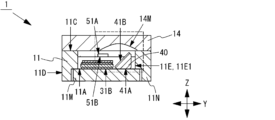
- 3 is a cross-sectional view of the light emitting device according to the first embodiment taken along line III-III in FIG. 1.
- 4 is a cross-sectional view of the light emitting device according to the first embodiment, the sixth embodiment, and the seventh embodiment taken along line IV-IV in FIG.
- FIG. 2 is a top view showing a see-through state of a lid in the light-emitting device according to the first and second embodiments.
- FIG. 4 is an enlarged view of the rectangular dashed line portion in FIG. 3 .
- 3 is a diagram for explaining an example of an optical path of light in the light emitting device according to the first embodiment.
- FIG. 6 is a diagram for explaining another example of the optical path of light in the light emitting device according to the first embodiment.
- FIG. FIG. 13 is a perspective view of the cover according to each embodiment except for the sixth embodiment, as viewed from the side on which the lens surface is provided.
- FIG. 13 is a top view of the cover according to each embodiment except for the sixth embodiment, as viewed from the side on which the lens surface is provided.
- FIG. 13 is a perspective view showing the structure inside the package of the light emitting device according to each embodiment except for the seventh embodiment.
- FIG. 13 is a top view showing the structure inside the package of the light emitting device according to each embodiment except for the seventh embodiment.
- FIG. 4 is a bottom view of the package according to each embodiment.
- 3 is a top view showing an arrangement of a semiconductor laser element and a submount according to each embodiment.
- FIG. FIG. 2 is a side view showing an arrangement of the semiconductor laser element and the submount according to each embodiment.
- FIG. 6 is a cross-sectional view of a light emitting device according to a second embodiment.
- FIG. 11 is a perspective view of a light emitting device according to a third embodiment.
- FIG. 11 is a cross-sectional view of a light emitting device according to a third embodiment.
- FIG. 13 is a top view of a light emitting device according to a fourth embodiment.
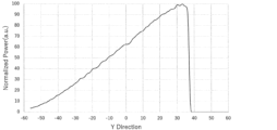
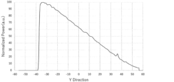
- FIG. 13 is a cross-sectional view of a light emitting device according to a fourth embodiment. 13 is a schematic diagram of a light-emitting module according to a fifth embodiment. FIG. FIG. 13 is a cross-sectional view of a light emitting device according to a sixth embodiment. FIG. 13 is a diagram showing the light intensity distribution of the first light of the light emitting device according to the sixth embodiment. FIG. 13 is a diagram showing a light intensity distribution of a second light of the light emitting device according to the sixth embodiment. FIG. 13 is a diagram showing a more uniform light intensity distribution of light emitted from the light emitting device according to the sixth embodiment. FIG. 13 is a cross-sectional view of a light emitting device according to a seventh embodiment.
- polygons such as triangles and quadrangles are referred to as polygons, including shapes in which the corners have been processed by rounding, chamfering, removing corners, rounding, etc. Furthermore, shapes in which processing has been applied to the middle part of a side, not just the corners (edges), are also referred to as polygons. In other words, shapes that have been partially processed while retaining the base polygon are included in the interpretation of "polygon" described in this specification and claims.
- directions such as the X direction, Y direction, and Z direction may be indicated by arrows.
- the directions of these arrows are consistent between multiple drawings relating to the same embodiment.
- the direction of the arrow marked with X, Y, and Z is the positive direction
- the opposite direction is the negative direction.
- a direction marked with X at the end of an arrow is the X direction and is also the positive direction.
- a direction that is both the X direction and the positive direction is referred to as the "positive X direction”
- the opposite direction is referred to as the "negative X direction.”
- X direction it is meant to include both the positive and negative directions.
- the description describing "one or each" object is a description that combines a description of one object in an embodiment with one object, a description of one object in an embodiment with multiple objects, and a description of each of the multiple objects in an embodiment with multiple objects. Therefore, the description describing "one or each" object supports all of the following: in an embodiment with one object, this one object has explanatory content; in an embodiment with multiple objects, at least one of these objects has explanatory content; in an embodiment with multiple objects, each of these multiple objects has explanatory content; and in an embodiment with one or multiple objects, all of the objects have explanatory content.
- component refers to an object that is physically handled as a single unit.
- An object that is physically handled as a single unit can also be said to be an object that is handled as a single part in the manufacturing process.
- a “part” refers to an object that does not need to be physically handled as a single unit.
- “part” is used when referring to a portion of a single component, or when referring to multiple components collectively as a single object.
- FIGS. 1 to 13 are drawings for explaining an exemplary embodiment of the light emitting device 1.
- FIG. 1 is a perspective view of the light emitting device 1.
- FIG. 2 is a side view of the light emitting device 1.
- FIG. 3 is a cross-sectional view taken along line III-III in FIG. 1. The rectangular dashed lines indicate the area shown in an enlarged manner in FIG. 6A.
- FIG. 4 is a cross-sectional view taken along line IV-IV in FIG. 1. The wiring 60 is omitted from the cross-sectional views of FIGS. 3 and 4.
- FIG. 5 is a top view of the light emitting device 1 with the lid 14 in a transparent state. The lid 14 is shown by a dotted line.
- FIG. 6A is an enlarged view of the dashed rectangular portion in FIG. 3.
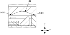
- FIG. 6B is a diagram for explaining an example of the optical path LP of light in the light emitting device 1.
- FIG. 6C is a diagram for explaining another example of the optical path LP of light in the light emitting device 1.
- the optical path LP is shown by a wavy line in FIGS. 6B and 6C.
- a virtual plane passing through the first inner side surface 11E1 of the frame portion 11N and parallel to the first inner side surface 11E1 is indicated by a broken line.
- Fig. 7 is a perspective view of the cover 14 as viewed from the side on which the lens surface 14M is provided.
- Fig. 8 is a top view of the cover 14 as viewed from the side on which the lens surface is provided. In Figs. 7 and 8, the optical axis LA of the lens surface 14M is indicated by a dotted line.
- Fig. 9 is a perspective view showing the internal structure of the package of the light emitting device 1.
- Fig. 10 is a top view showing the internal structure of the package of the light emitting device 1.
- Fig. 11 is a bottom view of the package 10.
- Fig. 12 is a top view showing the arrangement of the semiconductor laser element 20 and the submount 30.
- Fig. 13 is a side view showing the arrangement of the semiconductor laser element 20 and the submount 30.
- the light emitting device 1 comprises a number of components. These components include a package 10, one or more semiconductor laser elements 20, one or more submounts 30, one or more reflecting members 40, one or more protective elements 50, and a number of wirings 60.
- the light emitting device 1 may include other components.
- the light emitting device 1 may include a semiconductor laser element in addition to the one or more semiconductor laser elements 20.
- the light emitting device 1 may not include some of the components listed here.
- the package 10 includes a base body 11 and a lid body 14.
- the lid body 14 is joined to the base body 11 to form the package 10.
- An internal space in which other components are disposed is defined in the package 10.
- This internal space is a closed space surrounded by the base body 11 and the lid body 14.
- this internal space can be a space that is sealed in a vacuum or airtight state.
- the outer edge shape of the package 10 is rectangular.
- This rectangle can be a rectangle having long and short sides.
- the short side direction of this rectangle is the same as the X direction
- the long side direction is the same as the Y direction. Note that when viewed from above, the outer edge shape of the package 10 does not have to be rectangular.
- an internal space is formed in which other components are arranged.
- the first top surface 11A of the package 10 is part of the area that defines the internal space.
- each of the inner sides 11E and the bottom surface 14B of the package 10 are part of the area that defines the internal space.
- the base 11 has a first upper surface 11A and a lower surface 11B.
- the base 11 has a second upper surface 11C.
- the base 11 has one or more outer surfaces 11D.
- the base 11 has one or more inner surfaces 11E.
- the one or more outer surfaces 11D intersect with the second upper surface 11C.
- the one or more outer surfaces 11D intersect with the lower surface 11B.
- the one or more inner surfaces 11E intersect with the second upper surface 11C.
- the outer edge shape of the base 11 is rectangular.
- the outer edge shape of the base 11 is the outer edge shape of the package 10.
- the outer edge shape of the first top surface 11A is rectangular. This rectangle can be a rectangle having long and short sides. The long side direction of the first top surface 11A and the long side direction of the outer edge shape of the base 11 are parallel. Note that when viewed from above, the outer edge shape of the first top surface 11A does not have to be rectangular.
- the first top surface 11A is surrounded by the second top surface 11C.
- the second top surface 11C is an annular surface that surrounds the first top surface 11A when viewed from above.
- the second top surface 11C is a rectangular annular surface.
- the frame defined by the inner edge of the second top surface 11C is referred to as the inner frame of the second top surface 11C
- the frame defined by the outer edge of the second top surface 11C is referred to as the outer frame of the second top surface 11C.
- the base 11 has a recess surrounded by a frame by the second top surface 11C.
- the recess defines a portion of the base 11 that is recessed below the second top surface 11C.
- the first top surface 11A is part of the recess.
- One or more inner surfaces 11E are part of the recess.
- the second top surface 11C is located above the first top surface 11A.
- the base 11 has one or more step portions 11F.
- the step portion 11F has an upper surface 11G and a side surface 11H that intersects with the upper surface 11G and extends downward from the upper surface 11G.
- one step portion 11F has only one upper surface 11G and one side surface 11H.
- the upper surface 11G intersects with the inner surface 11E.
- the side surface 11H intersects with the first upper surface 11A.
- the or each step portion 11F is provided inside the inner frame of the second top surface 11C when viewed from above.
- the or each step portion 11F is formed along a part or all of the inner side surface 11E when viewed from above.
- the side surface 11H is an inner side surface, but the side surface 11H and the inner side surface 11E are different surfaces.
- the or each inner side surface 11E and the or each side surface 11H are perpendicular to the first top surface 11A.
- the perpendicular allows for a difference of ⁇ 3 degrees.
- the one or more step portions 11F may include a first step portion 11F1 and a second step portion 11F2.
- the first step portion 11F1 and the second step portion 11F2 are provided at positions where their respective side surfaces 11H face each other.
- the first step portion 11F1 and the second step portion 11F2 are provided on the short side of the inner frame of the second upper surface 11C.
- the base 11 has a base portion 11M and a frame portion 11N.
- the base portion 11M and the frame portion 11N may be made of different materials.
- the base 11 may be configured to include a base member corresponding to the base portion 11M and a frame member corresponding to the frame portion 11N.
- the base portion 11M includes a first upper surface 11A.
- the frame portion 11N includes a second upper surface 11C.
- the frame portion 11N includes one or more outer surfaces 11D and one or more inner surfaces 11E.
- the frame portion 11N includes one or more step portions 11F.
- the underside of the base 11M constitutes a part or all of the area of the underside 11B of the base 11.
- the underside of the frame 11N constitutes the remaining area of the underside 11B of the base.
- the base 11 has a plurality of wiring portions 12A.
- the plurality of wiring portions 12A includes one or more first wiring portions 12A1 arranged in the internal space of the package 10 and one or more second wiring portions 12A2 provided on the outer surface of the package 10.
- One or each of the first wiring portions 12A1 is provided on the upper surface 11G of the step portion 11F.
- the base 11 has one or more first wiring portions 12A1 provided on the upper surface 11G of the first step portion 11F1.
- the base 11 has one or more first wiring portions 12A1 provided on the upper surface 11G of the second step portion 11F2.
- One or each of the second wiring parts 12A2 is provided on the bottom surface 11B of the package 10.
- One or each of the second wiring parts 12A2 is provided on the bottom surface of the frame part 11N. Note that the second wiring parts 12A2 may be provided on an outer surface other than the bottom surface 11B of the package 10.
- the base 11 When the base 11 is divided into two regions by a virtual line passing through the side surface 11H of the first step portion 11F1 and parallel to this side surface 11H, the base 11 has one or more second wiring portions 12A2 provided on the lower surface 11B of the base 11 in the region that includes the upper surface 11G of the first step portion 11F1.
- the base 11 When the base 11 is divided into two regions by a virtual line passing through the side surface 11H of the second step portion 11F2 and parallel to this side surface 11H in a top view, the base 11 has one or more second wiring portions 12A2 provided on the bottom surface 11B of the base 11 in the region that includes the top surface 11G of the second step portion 11F2.
- one or each of the first wiring parts 12A1 is electrically connected to the second wiring part 12A2.
- One or more of the first wiring parts 12A1 are electrically connected to different second wiring parts 12A2.
- the base 11 has a bonding pattern 13A.
- the bonding pattern 13A is provided on the second upper surface 11C.
- the bonding pattern 13A is provided in a ring shape.
- the bonding pattern 13A is provided in a rectangular ring shape. In a top view, the first upper surface 11A is surrounded by the bonding pattern 13A.
- the base 11 can be formed, for example, using ceramic as the main material.
- ceramics that can be the main material of the base 11 include aluminum nitride, silicon nitride, aluminum oxide, and silicon carbide.
- the main material refers to the material that occupies the largest proportion of the mass or volume of the target formation. Note that when the target formation is formed from a single material, that material is the main material. In other words, when a material is the main material, it includes the possibility that the proportion of that material could be 100%.
- the base 11 may be formed using a base member and a frame member that are formed using different main materials.
- the base member may be formed using, for example, a material with excellent heat dissipation properties as the main material, such as a metal or a composite containing a metal, graphite, or diamond.
- metals that are the main material of the base member include copper, aluminum, or iron.
- composites containing a metal that are the main material of the base member include copper molybdenum or copper tungsten.
- the frame member may be formed, for example, using, for example, a ceramic listed above as the main material of the base 11 as the main material.
- the wiring section 12A can be formed, for example, using a metal material as the main material.
- the metal material that is the main material of the wiring section 12A include elemental metals such as Cu, Ag, Ni, Au, Ti, Pt, Pd, Cr, and W, or alloys containing these metals.
- the wiring section 12A can be composed of, for example, one or more metal layers.
- the bonding pattern 13A can be formed, for example, using a metal material as the main material.
- the metal material that is the main material of the bonding pattern 13A include elemental metals such as Cu, Ag, Ni, Au, Sn, Ti, and Pd, or alloys containing these metals.
- the bonding pattern 13A can be composed of, for example, one or more metal layers.
- the lid 14 has an upper surface 14A, a lower surface 14B, and a lens surface 14M.
- the lid 14 also has one or more side surfaces 14C.
- the lid 14 is configured in a shape in which a lens surface is provided on one surface of a rectangular flat plate.
- the outer edge shape of the lid 14 is rectangular when viewed from above. This rectangle can be a rectangle with long and short sides. When viewed from above, the long side direction of the outer edge shape of the lid 14 and the long side direction of the outer edge shape of the base 11 are parallel to each other. Note that when viewed from above, the outer edge shape of the lid 14 does not have to be rectangular.
- Lens surface 14M of cover 14 is formed on the lower surface 14B side.
- Lens surface 14M is formed concave toward upper surface 14A.
- Lens surface 14M is formed above an imaginary plane that includes and is parallel to lower surface 14B.
- Lens surface 14M is a concave lens surface that is concave upward from lower surface 14B.
- Lens surface 14M is a cylindrical lens surface. Therefore, lens surface 14M has no curvature in a certain direction. In other words, lens surface 14M has zero curvature in this certain direction. Note that lens surface 14M does not have to be a cylindrical lens surface that has no curvature in a certain direction in the strict sense. Due to manufacturing reasons, it is possible that the lens surface 14M may have a slight curvature in this certain direction. In the illustrated lens surface 14M of the lid body 14, the direction in which it has substantially no curvature is the same as the X direction.
- Lens surface 14M has a curvature in a first direction.
- Lens surface 14M has no curvature in a second direction perpendicular to the first direction.
- Lens surface 14M has a curvature in the long side direction of lid body 14.
- Lens surface 14M has no curvature in the short side direction of lid body 14.
- the first direction is the same as the Y direction
- the second direction is the same as the X direction. Note that lens surface 14M may have a curvature in the second direction.
- the optical axis of the curved lens surface in the first direction is referred to as the optical axis LA of the lens on lens surface 14M.
- the optical axis LA of the lens appears as a straight line extending in the second direction. In other words, any point on this straight line may be referred to as the optical axis LA of the lens.
- the lens surface 14M is located at the uppermost point where the lens optical axis LA passes.
- the lens surface 14M is formed in the lid 14 so that it is concave upward.
- the thickness of the lid 14 is at its thinnest at the optical axis LA of the lens surface 14M.
- the distance from the bottom surface 14B of the lid 14 to the optical axis of the lens surface 14M is 20% or more and 60% or less of the width (thickness) from the top surface 14A to the bottom surface 14B of the lid 14.
- the greater this distance the larger the area over which the lens surface 14M is formed can be secured, making it easier for light to be incident on the lens surface 14M.
- the thickness of the lid 14 is not constant but varies, the thinner parts may be more susceptible to damage than the thicker parts. Taking these factors into consideration, the above-mentioned range of 20% or more and 60% or less may be an example of an appropriate numerical range for the shape of the lid 14 shown in the figure.
- the width of lens surface 14M of lid body 14 is 30% or more and 80% or less of the width of lid body 14.
- the larger this width of lens surface 14M the easier it is for light to be incident on lens surface 14M.
- the larger this width of lens surface 14M the lower the overall strength of lid body 14 may be. Taking these factors into consideration, the above-mentioned range of 30% or more and 80% or less may be an example of an appropriate numerical range for the shape of lid body 14 shown in the figure.
- the width of lens surface 14M of lid body 14 is 20% or more and 70% or less of the width of lid body 14.
- the ratio of the width of lens surface 14M to the width of cover body 14 in the first direction is smaller than the ratio of the width of lens surface 14M to the width of cover body 14 in the second direction.
- the width of lens surface 14M in the first direction is larger than the width of lens surface 14M in the second direction.
- the optical axis LA of lens surface 14M does not overlap with the midpoint of the width of lid body 14 in the first direction.
- the optical axis LA of lens surface 14M is located in one of the regions when lid body 14 is divided into two regions by a line that passes through the midpoint of the width of lid body 14 in the first direction and is parallel to the second direction. Furthermore, when this one region is further divided into two regions by a line that passes through the midpoint of the width of this one region in the first direction and is parallel to the second direction, the optical axis LA of lens surface 14M is located in region R1 closer to the midpoint of the width of lid body 14 in the first direction.
- the cover 14 further has one or more first inner surfaces 14D1.
- the one or each of the first inner surfaces 14D1 is connected to the lens surface 14M.
- the one or each of the first inner surfaces 14D1 is connected to the bottom surface 14B.
- the one or each of the first inner surfaces 14D1 is not a surface having an effective lens function.
- the one or each of the first inner surfaces 14D1 is an inner surface that extends in the second direction when viewed from above.
- the one or each of the first inner surfaces 14D1 is an edge located at the end of the lens surface 14M in the first direction and intersects with an edge extending in the second direction.
- the one or more first inner surfaces 14D1 include a first inner surface 14D1 located at an end of the lens surface 14M in the positive Y direction and intersecting with a side extending in the second direction. Furthermore, the one or more first inner surfaces 14D1 include a first inner surface 14D1 located at an end of the lens surface 14M in the negative Y direction and intersecting with a side extending in the second direction. For example, if the positive Y direction is the first direction, the negative Y direction can be said to be the direction opposite to the first direction.
- the width of the first inner surface 14D1 is more than 0% and not more than 30% of the distance from the bottom surface 14B of the lid body 14 to the optical axis LA of the lens surface 14M. As this width of the first inner surface 14D1 increases, the lid body 14 becomes thinner, so it may be preferable not to make this width too large. Alternatively, if one tries to maintain the thickness of the lid body 14, the width of the lens surface 14M in the first direction will become smaller. For the shape of the lid body 14 shown in the figure, it may be preferable to make the width of the first inner surface 14D1 not more than 30%.
- the or each first inner surface 14D1 extends vertically upward relative to the bottom surface 14B. Note that "vertical” here includes a difference of ⁇ 5 degrees.
- the cover 14 further has two second inner surfaces 14D2.
- One or each of the second inner surfaces 14D2 is connected to the lens surface 14M.
- the one or each of the second inner surfaces 14D2 is connected to the optical axis of the lens surface 14M at the outer edge of the lens surface 14M.
- the one or each of the second inner surfaces 14D2 is connected to the bottom surface 14B.
- the one or each of the second inner surfaces 14D2 does not have an effective lens function.
- the one or each of the second inner surfaces 14D2 is an inner surface that extends in the first direction when viewed from above.
- One or each of the second inner surfaces 14D2 extends obliquely upward relative to the bottom surface 14B.
- the angle between the bottom surface 14B and the second inner surface 14D2 is an obtuse angle. Therefore, in a top view, the side connecting the second inner surface 14D2 and the lens surface 14M does not overlap with the bottom surface 14B.
- the width of the lens surface 14M in the second direction is shortest at a position passing through the optical axis of the lens surface 14M.
- the lid 14 is bonded to the base 11.
- the bottom surface 14B of the lid 14 is bonded to the second top surface 11C of the base 11.
- the lid 14 is bonded to the bonding pattern 13A of the base 11.
- the lid 14 is bonded to the base 11 via an adhesive.
- a portion of the lens surface 14M overlaps with the second upper surface 11C of the base 11 in a top view.
- a portion of the lens surface 14M overlaps with the bonding pattern 13A of the base 11 in a top view.
- a portion of the outer edge of the lens surface 14M is located inside the outer surface 11D and outside the inner surface 11E of the base 11 in a top view.
- the width in the first direction of the area where the lens surface 14M and the second upper surface 11C overlap in a top view is more than 0% and not more than 15% of the width in the first direction of the lens surface 14M. By limiting this width, it becomes easier to ensure an area where the second upper surface 11C and the lower surface 14B are bonded via adhesive.
- the one or more first inner surfaces 14D1 of the lid 14 include a first inner surface 14D1 that overlaps with the second upper surface 11C in a top view.
- the lens surface 14M does not extend to the lower surface 14B, so that the area where the second upper surface 11C of the base 11 and the lower surface 14B of the lid 14 overlap in a top view can be increased, and poor bonding between the base 11 and the lid 14 can be suppressed.
- the first inner surface 14D1 can prevent the adhesive used for bonding from reaching the lens surface 14M.
- the one or more inner surfaces 11E of the base 11 include an inner surface 11E that overlaps with the lens surface 14M in a top view. There is only one inner surface 11E that overlaps with the lens surface 14M in a top view. This inner surface 11E is referred to as the first inner surface 11E1 of the base 11. It can be said that the inner surfaces 11E other than the first inner surface 11E1 do not overlap with the lens surface 14M in a top view. Note that the base 11 may have an inner surface 11E that overlaps with the lens surface 14M in a top view in addition to the first inner surface 11E1.
- the lens surface 14M does not overlap with the bonding pattern 13A provided on the second upper surface 11C.
- the first inner surface 14D1 of the lid 14 does not overlap with the bonding pattern 13A.
- the lid body 14 has translucency, which allows light to pass through.
- translucency means that the transmittance of light incident on the lid body 14 is 80% or more.
- the lid body 14 may have a non-translucent region (a region that does not have translucency) in part.
- the lid 14 can be formed, for example, using glass as the main material.
- the lid 14 can also be formed, for example, using sapphire as the main material.
- the outer edge shape of the base 11 is wider in the first direction than in the second direction when viewed from above.
- the inner edge shape of the second upper surface 11C is wider in the first direction than in the second direction when viewed from above.
- the semiconductor laser element 20 has an upper surface 21A, a lower surface 21B, and a plurality of side surfaces 21C.
- the shape of the upper surface 21A is a rectangle having long sides and short sides.
- the outer shape of the semiconductor laser element 20 in the top view is a rectangle having long sides and short sides. Note that the shape of the upper surface 21A and the outer shape of the semiconductor laser element 20 in the top view are not limited to this.
- the semiconductor laser element 20 has a light emitting surface 22 that emits light.
- the side surface 21C can be the light emitting surface 22.
- the side surface 21C that becomes the light emitting surface 22 intersects with a short side of the top surface 21A.
- the top surface 21A can be the light emitting surface 22.
- the semiconductor laser element 20 can be a single-emitter semiconductor laser element with one emitter. Also, the semiconductor laser element 20 can be a multi-emitter semiconductor laser element with multiple emitters.
- a semiconductor laser element that emits blue light can be used as the semiconductor laser element 20.
- a semiconductor laser element that emits green light can be used as the semiconductor laser element 20.
- a semiconductor laser element that emits red light can be used as the semiconductor laser element 20.
- a semiconductor laser element that emits light of other colors or wavelengths may also be used as the semiconductor laser element 20.
- blue light refers to light whose peak emission wavelength is in the range of 420nm to 494nm.
- Green light refers to light whose peak emission wavelength is in the range of 495nm to 570nm.
- Red light refers to light whose peak emission wavelength is in the range of 605nm to 750nm.
- the semiconductor laser element 20 that emits blue light or the semiconductor laser element 20 that emits green light there is a semiconductor laser element that includes a nitride semiconductor.
- a nitride semiconductor for example, GaN-based semiconductors such as GaN, InGaN, and AlGaN can be used.
- the semiconductor laser element 20 that emits red light there are semiconductor laser elements that include InAlGaP-based, GaInP-based, and GaAs-based semiconductors such as GaAs and AlGaAs.
- the semiconductor laser element 20 emits directional laser light. Diverging light with a spreading property is emitted from the light emission surface 22 (emitting end surface) of the semiconductor laser element 20.
- the light emitted from the semiconductor laser element 20 forms an elliptical far-field pattern (hereinafter referred to as "FFP") in a plane parallel to the light emission surface 22.
- the FFP refers to the shape and light intensity distribution of the emitted light at a position away from the light emission surface of the semiconductor laser element.
- the light passing through the center of the elliptical shape of the FFP in other words, the light with the peak intensity in the light intensity distribution of the FFP, is referred to as the light traveling along the optical axis or the light passing through the optical axis.
- the light having an intensity of 1/e2 or more with respect to the peak intensity value is referred to as the main part of the light.
- the shape of the FFP of the light emitted from the semiconductor laser element 20 is an ellipse in which the stacking direction is longer than the direction perpendicular to the stacking direction on a plane parallel to the light emission surface 22.
- the stacking direction is the direction in which multiple semiconductor layers including the active layer are stacked in the semiconductor laser element 20.
- the direction perpendicular to the stacking direction can also be called the surface direction of the semiconductor layers.
- the long axis direction of the elliptical shape of the FFP can also be called the fast axis direction of the semiconductor laser element 20, and the short axis direction can also be called the slow axis direction of the semiconductor laser element 20.
- the spread angle of light of 1/ e2 of the peak light intensity based on the light intensity distribution of the FFP is defined as the spread angle of light of the semiconductor laser element 20.
- the spread angle of light is indicated by the angle formed by light of the peak light intensity (light passing through the optical axis) and light of the light intensity of 1/ e2 of the peak light intensity.
- the spread angle of light may also be obtained from the light intensity of half the peak light intensity, for example.
- the term "spread angle of light” refers to the spread angle of light at the light intensity of 1/ e2 of the peak light intensity.
- the divergence angle of the light emitted from the semiconductor laser element 20 in the fast axis direction can be 15 degrees or more and less than 40 degrees.
- the divergence angle of this light in the slow axis direction can be more than 0 degrees and less than 10 degrees.
- the divergence angle of this light in the fast axis direction is greater than the divergence angle of the light in the slow axis direction.
- the spread angle in the fast axis direction of blue light emitted from the semiconductor laser element 20 can be 15 degrees or more and less than 30 degrees, and the spread angle in the slow axis direction can be 2 degrees or more and less than 10 degrees.
- the spread angle in the fast axis direction of green light emitted from the semiconductor laser element 20 can be 15 degrees or more and less than 30 degrees, and the spread angle in the slow axis direction can be 2 degrees or more and less than 10 degrees.
- the spread angle in the fast axis direction of red light emitted from the semiconductor laser element 20 can be 20 degrees or more and less than 40 degrees, and the spread angle in the slow axis direction can be 3 degrees or more and less than 10 degrees.
- the submount 30 has an upper surface 31A, a lower surface 31B, and one or more side surfaces 31C.
- the upper surface 31A can be said to be a mounting surface on which other components are mounted.
- the shape of the upper surface 31A is rectangular. This rectangle of the upper surface 31A can have short sides and long sides. Note that the shape of the upper surface 31A does not have to be rectangular.
- the outer shape of the submount 30 when viewed from above is rectangular. This rectangle of the submount 30 may have short sides and long sides. Note that the outer shape of the submount 30 when viewed from above does not have to be rectangular.
- the submount 30 may have an outer shape in which the length in one direction when viewed from above (hereinafter, this direction will be referred to as the short side direction of the submount 30) is smaller than the length in the direction perpendicular to that (hereinafter, this direction will be referred to as the long side direction of the submount 30).
- the short side direction is the same as the X direction
- the long side direction is the same as the Y direction.
- the submount 30 may be configured to include a substrate 32A and an upper metal member 32B.
- the submount 30 may further be configured to include a lower metal member 32C.
- the upper metal member 32B is provided on the upper surface side of the substrate 32A.
- the lower metal member 32C is provided on the lower surface side of the substrate 32A.
- the submount 30 further includes a wiring layer 33.
- the wiring layer 33 is provided on the upper metal member 32B.
- Substrate 32A is insulating.
- Substrate 32A is made of, for example, silicon nitride, aluminum nitride, or silicon carbide. It is advisable to select ceramic, which has relatively good heat dissipation properties (high thermal conductivity), as the main material for substrate 32A.
- the upper metal member 32B is primarily made of a metal such as copper or aluminum.
- the upper metal member 32B has one or more metal layers.
- the upper metal member 32B may have multiple metal layers made primarily of different metals.
- the lower metal member 32C is primarily made of a metal such as copper or aluminum.
- the lower metal member 32C has one or more metal layers.
- the lower metal member 32C may have multiple metal layers made primarily of different metals.
- the wiring layer 33 can be formed using a metal.
- the wiring layer 33 can be formed using AuSn solder (a metal layer of AuSn).
- the length of the submount 30 in the short side or lateral direction is 700 ⁇ m or more and 1400 ⁇ m or less.
- the length of the submount 30 in the long side or longitudinal direction is 1200 ⁇ m or more and 2700 ⁇ m or less.
- the difference between the length of the submount 30 in the longitudinal direction and the length of the submount 30 in the lateral direction is 100 ⁇ m or more and 2000 ⁇ m or less.
- the thickness of the submount 30 (width in the direction perpendicular to the upper surface 31A) is 200 ⁇ m or more and 400 ⁇ m or less.
- the thickness of the substrate 32A is 100 ⁇ m or more and 300 ⁇ m or less.
- the thickness of the upper metal member 32B is 25 ⁇ m or more and 75 ⁇ m or less.
- the thickness of the lower metal member 32C is 25 ⁇ m or more and 75 ⁇ m or less.
- the thickness of the wiring layer 33 is 1 ⁇ m or more and 5 ⁇ m or less.
- the reflecting member 40 has a lower surface 41A and a light reflecting surface 41B that reflects light.
- the light reflecting surface 41B is inclined with respect to the lower surface 41A.
- a straight line connecting the lower end and the upper end of the light reflecting surface 41B is inclined with respect to the lower surface 41A.
- the angle at which the light reflecting surface 41B is inclined with respect to the lower surface 41A is referred to as the inclination angle of the light reflecting surface 41B.
- Light reflecting surface 41B is a flat surface. Note that light reflecting surface 41B may be a curved surface. The inclination angle of light reflecting surface 41B is 45 degrees. Note that the inclination angle of light reflecting surface 41B does not have to be 45 degrees.
- the main material of the reflective member 40 can be glass or metal. It is advisable to use a heat-resistant material as the main material of the reflective member 40.
- the main material can be, for example, glass such as quartz or BK7 (borosilicate glass), or metal such as Al.
- the reflective member 40 can also be formed using Si as the main material.
- the light reflecting surface 41B can be formed from the main material.
- the general shape of the reflecting member 40 may be formed from the main material, and the light reflecting surface 41B may be formed on the surface of the general shape.
- the light reflecting surface 41B can be formed using, for example, a metal layer such as Ag or Al, or a dielectric multilayer film such as Ta2O5 / SiO2 , TiO2 / SiO2 , or Nb2O5 / SiO2 .
- the light reflecting surface 41B has a reflectance of 90% or more for the peak wavelength of light irradiated onto the light reflecting surface 41B. This reflectance may also be 95% or more. This reflectance can also be 99% or more. The light reflectance is 100% or less or is less than 100%.
- the protective element 50 has an upper surface 51A, a lower surface 51B, and one or more side surfaces 51C.
- the protective element 50 has a rectangular parallelepiped shape. However, the protective element 50 does not have to have a rectangular parallelepiped shape.
- the protective element 50 is intended to prevent an excessive current from flowing through a particular element (e.g., a semiconductor laser element) and causing the element to be destroyed.
- An example of the protective element 50 is a Zener diode.
- a Zener diode made of Si can be used.
- the wiring 60 is a linear conductive material having joints at both ends. The joints at both ends become joints with other components.
- the wiring 60 is used for electrical connection between two components.
- the wiring 60 is, for example, a metal wire. Examples of the metal that can be used include gold, aluminum, silver, and copper.
- the or each semiconductor laser element 20 is disposed on the base 11.
- the or each semiconductor laser element 20 is disposed on the first upper surface 11A.
- the or each semiconductor laser element 20 is disposed in the internal space of the package 10.
- the or each semiconductor laser element 20 is disposed in a sealed space surrounded by the base 11 and the lid 14.
- Light emitted from one or each semiconductor laser element 20 is incident on the lens surface 14M of the cover 14.
- the light emitted from the semiconductor laser element 20 is incident on the lens surface 14M so that the fast axis direction of the light is parallel to the first direction of the lens surface 14M.
- the light emitted from the semiconductor laser element 20 is incident on the lens surface 14M so that the slow axis direction of the light is parallel to the second direction of the lens surface 14M.
- Lens surface 14M has a curvature in the first direction that diffuses the light emitted from semiconductor laser element 20 and incident on lens surface 14M.
- Cover 14 further diffuses the fast axis direction of the light emitted from semiconductor laser element 20 and incident on lens surface 14M, causing it to exit from top surface 14A.
- ⁇ 1 the spread angle in the fast axis direction of the light about to enter lens surface 14M
- ⁇ 2 the spread angle in the fast axis direction of the light emitted from top surface 14A
- ⁇ 2 is larger than ⁇ 1. This allows light to be emitted from light emitting device 1 at a spread angle in the fast axis direction that is larger than the spread angle of light emitted from light exit surface 22 of semiconductor laser element 20.
- ⁇ 2 is greater than 1.0 and less than or equal to 2.5 times ⁇ 1.
- the curvature of the lens increases and the thickness of the lid 14 at the optical axis of the lens becomes thinner.
- the value may be preferable to set the value to 2.5 times or less.
- the spread angle in the fast axis direction of the light emitted from the lid 14 is 1.1 to 2.5 times the spread angle in the fast axis direction of the light emitted from the semiconductor laser element 20.
- the spread angle ( ⁇ 2) in the fast axis direction of the light emitted from the lid 14 is 38 degrees to 95 degrees.
- the spread angle ( ⁇ 2) in the fast axis direction of blue light emitted from the semiconductor laser element 20 and the lid body 14 can be 38 degrees or more and 95 degrees or less.
- the spread angle ( ⁇ 2) in the fast axis direction of green light emitted from the semiconductor laser element 20 and the lid body 14 can be 38 degrees or more and 95 degrees or less.
- the spread angle ( ⁇ 2) in the fast axis direction of red light emitted from the semiconductor laser element 20 and the lid body 14 can be 49 degrees or more and 95 degrees or less.
- Lens surface 14M diffuses the light emitted from semiconductor laser element 20 and incident on lens surface 14M less in the second direction than in the first direction.
- the spread angle in the slow axis direction of the light incident on lens surface 14M is ⁇ 3 and the spread angle in the slow axis direction of the light emitted from top surface 14A is ⁇ 4, then the value obtained by dividing ⁇ 4 by ⁇ 3 ( ⁇ 4/ ⁇ 3) is smaller than the value obtained by dividing ⁇ 2 by ⁇ 1 ( ⁇ 2/ ⁇ 1).
- lens surface 14M does not have a curvature in the second direction, ⁇ 4 and ⁇ 3 are equal, and the value of ⁇ 4/ ⁇ 3 is 1. It is preferable that the value of ⁇ 4/ ⁇ 3 is 1 or less.
- light emitted from semiconductor laser element 20 as diverging light may be made to narrow by being incident on lens surface 14M, and then emitted from cover body 14.
- lens surface 14M When using lens surface 14M to collimate light or focus it at a desired point, precision in the mounting position of lens surface 14M is required. On the other hand, when realizing a sealed space by joining lid body 14 and base 11, sufficient adhesion between base 11 and lid body 14 is required to prevent gas from entering. When precision in the mounting position is required, it is preferable to adjust the position, but there are cases where sufficient positional precision cannot be achieved to achieve sufficient adhesion. Providing lens surface 14M for the purpose of diffusion rather than collimation or focusing at a specific position is compatible with achieving both a sealed space and lens function in lid body 14.
- lens surface 14M a cylindrical lens surface, it is possible to concentrate the lens action in a specific direction.
- the objective is only to diffuse the light in the fast axis direction, and there is no need to pay special attention to optical control in the slow axis direction.
- This type of optical control is also compatible with not only realizing a sealed space in lid body 14, but also providing a lens function by lens surface 14M.
- lens surface 14M does not have to be a cylindrical lens surface, and may have a curvature in the second direction for the purpose of suppressing the spread of light, rather than for the purpose of concentrating light on a specific point.
- the first direction of the lens surface 14M and the fast axis direction of the light incident on the lens surface 14M are parallel, but the parallelism here allows an angle of 5 degrees or more between the first direction and the fast axis direction of the light. Furthermore, it is preferable that the parallelism here be 7 degrees or less even if an angle is created between the first direction and the fast axis direction of the light.
- the semiconductor laser element 20 emits light from each of a plurality of emitters.
- the plurality of emitters has a first emitter and a second emitter, and a first light is emitted from the first emitter and a second light is emitted from the second emitter.
- the fast axis directions of the first light and the second light are parallel to each other and aligned in the slow axis direction.
- Lens surface 14M which is a cylindrical surface, has no curvature in the second direction, and the cross-sectional shape of the lens surface in the first direction is uniform in the second direction. Therefore, the lens effect due to the curvature in the first direction can be imparted to the first and second lights in the same way, without having to consider the positional accuracy of the first and second lights in the second direction.
- one or each semiconductor laser element 20 is disposed on a submount 30.
- One or each semiconductor laser element 20 is disposed on the first upper surface 11A via the submount 30.
- One or each submount 30 is bonded to the first upper surface 11A at the lower surface 31B, and is bonded to the semiconductor laser element 20 at the upper surface 31A.
- the number of semiconductor laser elements 20 disposed on one submount 30 is one or more.
- One or each semiconductor laser element 20 has a light emitting surface 22 on the side surface 21C, and emits light laterally from the light emitting surface 22.
- One or each semiconductor laser element 20 emits light in a first direction.
- the positive Y direction can be considered to be the first direction.
- one or each of the reflecting members 40 is disposed on the base 11.
- the one or each of the reflecting members 40 is disposed in the internal space of the package 10.
- the one or each of the reflecting members 40 is disposed on the first upper surface 11A.
- the one or each of the reflecting members 40 is disposed at a position spaced apart from the semiconductor laser element 20 in the first direction.
- One or each of the reflecting members 40 reflects light emitted from the semiconductor laser element 20.
- One or each of the semiconductor laser elements 20 emits light toward the light reflecting surface 41B of the reflecting member 40.
- the light reflected by the light reflecting surface 41B is incident on the lens surface 14M. Note that the light emitted from the semiconductor laser element 20 may be incident on the lens surface 14M without using reflection by the reflecting member 40.
- the or each reflecting member 40 is spaced apart from the inner surface 11E of the package 10.
- the or each reflecting member 40 is arranged with the light reflecting surface 41B facing the light emitting surface 22 of the semiconductor laser element 20 and the side opposite the light reflecting surface 41B facing the first inner surface 11E1.
- Light passing through the optical axis emitted from one or each semiconductor laser element 20 is reflected by the reflecting member 40 in a direction perpendicular to the first upper surface 11A.
- the position where the light passing through the optical axis is irradiated onto the light reflecting surface 41B overlaps with the optical axis LA of the lens surface 14M.
- the position where the light, which is the main part of the light emitted from one or each semiconductor laser element 20 and is incident on the lens surface 14M at the position farthest from the optical axis LA in the first direction, passes through the lens surface 14M of the cover body 14 is inside one or more inner surfaces 11E of the base 11 in a top view (see FIG. 6B). Also, the position where this light passes through the upper surface 14A of the cover body 14 is outside the multiple inner surfaces 11E of the base 11 in a top view. In this way, the lens surface 14M can be effectively used to emit diffused light from the upper surface of the light emitting device 1. Also, this light is light reflected by the light reflecting surface 41B of the reflecting member 40. Also, this light passes through the first inner surface 11E1 of the base 11 and passes through a virtual plane parallel to the first inner surface 11E1. Note that the first direction here is the positive Y direction in the light emitting device 1 shown in the figure.
- the position where the light reflected by the light reflecting surface 41B at the upper end of the light reflecting surface 41B, which is the main part of the light emitted from one or each semiconductor laser element 20, passes through the lens surface 14M of the cover 14 is inside one or more inner surfaces 11E of the base 11 in a top view (see FIG. 6C). Also, the position where this light passes through the upper surface 14A of the cover 14 is outside the multiple inner surfaces 11E of the base 11 in a top view. In this way, the lens surface 14M can be effectively used to emit diffused light from the upper surface of the light emitting device 1. Also, this light is light reflected by the light reflecting surface 41B of the reflecting member 40. Also, this light passes through the first inner surface 11E1 of the base 11 and passes through a virtual plane parallel to the first inner surface 11E1. Note that the first direction here is the positive Y direction in the light emitting device 1 shown in the figure.
- one or each protective element 50 is disposed on the base 11.
- One or each protective element 50 is disposed in the internal space of the package 10.
- the one or more protective elements 50 include a protective element 50 disposed on the upper surface 11G of the step portion 11F of the base 11.
- the protective element 50 protects the semiconductor laser element 20 disposed on the base 11.
- the light emitting device 1 has a plurality of wirings 60 electrically connected to the semiconductor laser element 20.
- the plurality of wirings 60 includes one or more wirings 60 that are bonded to the semiconductor laser element 20.
- the plurality of wirings 60 includes one or more wirings 60 that are bonded to the first step portion 11F1 of the base 11.
- the plurality of wirings 60 includes one or more wirings 60 that are bonded to the second step portion 11F2 of the base 11.
- the multiple wirings 60 are joined to the first wiring portion 12A1 and electrically connect the semiconductor laser element 20 to the second wiring portion 12A2.
- FIGS. 2, 5, 7 to 14 are diagrams for explaining an exemplary embodiment of the light emitting device 2.
- FIG. 2 is a side view of the light emitting device 2.
- FIG. 5 is a top view of the light emitting device 2 with the lid 14 being transparent.
- the lid 14 is indicated by a dotted line.
- the hatched portion indicates a region R1, which will be described later.
- FIG. 7 is a perspective view of the lid 14 as viewed from the side where the lens surface 14M is provided.
- FIG. 8 is a top view of the lid 14 as viewed from the side where the lens surface is provided.
- the optical axis LA of the lens surface 14M is indicated by a dotted line.
- FIG. 9 is a perspective view showing the internal structure of the package of the light emitting device 2.
- FIG. 10 is a top view showing the internal structure of the package of the light emitting device 2.
- FIG. 11 is a bottom view of the package 10.
- FIG. 12 is a top view showing the arrangement of the semiconductor laser element 20 and the submount 30.
- Fig. 13 is a side view showing the arrangement of the semiconductor laser element 20 and the submount 30.
- Fig. 14 is a cross-sectional view of the light-emitting device 2. Note that the wiring 60 is omitted in the cross-sectional view of Fig. 14.
- the cross-sectional position of the cross-sectional view of the light-emitting device 2 in Fig. 14 corresponds to the cross-sectional view of the light-emitting device 1 in Fig. 3.
- the light emitting device 1 comprises a number of components. These components include a package 10A, one or more semiconductor laser elements 20, one or more submounts 30, one or more reflecting members 40, one or more protective elements 50, and a number of wirings 60.
- lens surface 14M of lid 14 is formed on top surface 14A.
- Lens surface 14M is formed recessed toward bottom surface 14B.
- Lens surface 14M is formed below an imaginary plane that includes top surface 14A and is parallel to top surface 14A.
- Lens surface 14M is a concave lens surface recessed downward from top surface 14A.
- the point on lens surface 14M that passes through the optical axis LA of the lens is located at the lowest position.
- Lens surface 14M is formed in the cover 14 so that it is recessed downward.
- the distance from the top surface 14A of the lid 14 to the optical axis of the lens surface 14M is 20% to 60% of the width (thickness) from the top surface 14A to the bottom surface 14B of the lid 14.
- One or each of the first inner surfaces 14D1 is connected to the top surface 14A.
- the width of the first inner surface 14D1 is greater than 0% and less than 30% of the distance from the top surface 14A of the lid 14 to the optical axis LA of the lens surface 14M.
- the or each first inner surface 14D1 extends perpendicularly downward relative to the top surface 14A. Note that "perpendicular” here includes a difference of ⁇ 5 degrees.
- One or each of the second inner surfaces 14D2 is connected to the top surface 14A.
- One or each of the second inner surfaces 14D2 extends obliquely downward relative to the top surface 14A. Furthermore, the angle between the top surface 14A and the second inner surface 14D2 is an obtuse angle. Therefore, when viewed from above, the edge connecting the second inner surface 14D2 and the lens surface 14M does not overlap with the top surface 14A.
- the orientation of the lid body 14 in the package 10A is different from the orientation of the lid body 14 in the package 10 of the light emitting device 1.
- the lens surface 14M is provided on the lower surface 14B side, but in the light emitting device 2, the lens surface 14M is provided on the upper surface 14A side.
- the light emitted from the semiconductor laser element 20 is incident on the lens surface 14M of the lid 14 and is emitted from the upper surface 14A, but in light-emitting device 2, the light emitted from the semiconductor laser element 20 is incident on the lower surface 14B of the lid 14 and is emitted from the lens surface 14M. Therefore, the light emitted from the semiconductor laser element 20 is emitted from the lens surface 14M instead of being incident on the lens surface 14M.
- the lens surface 14M By providing the lens surface 14M on the upper surface 14A side, the area where the lower surface 14B of the lid 14 and the second upper surface 11C of the base overlap in a top view becomes larger than that of the light emitting device 1. Furthermore, when bonding the base 11 and the lid 14, it is not necessary to consider the possibility that the adhesive will come into contact with the lens surface 14M. On the other hand, if the lens surface 14M is provided on the upper surface 14A side, the size of the lens surface 14M that must be secured to allow light to pass becomes larger than that of the light emitting device 1. Furthermore, due to differences in the optical path length until the light is incident on the lens surface 14M, even if the spread angle of the light that has passed through the lens surface 14M is the same, the mode of diffusion will differ. Taking these points into consideration, it can be determined whether the configuration of the light emitting device 1 or the configuration of the light emitting device 2 is preferable.
- FIGS. 1 to 13, 15, and 16 are drawings for explaining an exemplary embodiment of the light emitting device 3.
- FIGS. 1 to 13 are drawings of a light emitting device in a state where the wave plate 70 is removed from the light emitting device 3, and the light emitting device in a state where the wave plate 70 is removed from the light emitting device 3 is equivalent to the light emitting device 1. Therefore, the description of each figure may be made with reference to the description of the light emitting device 1.
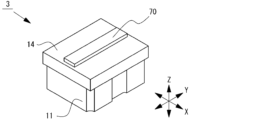
- FIG. 15 is a perspective view of the light emitting device 3.
- FIG. 16 is a cross-sectional view of the light emitting device 3. Note that the wiring 60 is omitted in the cross-sectional view of FIG. 16. Also, the cross-sectional position in the cross-sectional view of FIG. 16 of the light emitting device 3 corresponds to the cross-sectional view of FIG. 3 of the light emitting device 1.
- the light emitting device 3 includes a plurality of components.
- the plurality of components include a package 10, one or more semiconductor laser elements 20, one or more submounts 30, one or more reflecting members 40, one or more protective elements 50, a plurality of wirings 60, and a wave plate 70.
- the wave plate 70 changes the polarization state of the outgoing light relative to the incoming light.
- the wave plate 70 may be, for example, a half-wave plate that rotates the polarization direction of linearly polarized light, or a quarter-wave plate that converts linearly polarized light into circularly polarized light.
- a half-wave plate may be used as the wave plate 70.
- the wave plate 70 has an upper surface 71A, a lower surface 71B, and one or more side surfaces 71C.
- the wave plate 70 is formed in the shape of a flat plate.
- the outer edge shape of the wave plate 70 when viewed from above is a rectangle with long and short sides. Note that the shape does not have to be rectangular, but may be, for example, an ellipse, with one side longer than the other.
- a wave plate 70 is disposed on the upper surface 14A of the package 10.
- the wave plate 70 is bonded to the upper surface 14A.
- the wave plate 70 is bonded to the lid 14 via an adhesive.
- the wave plate 70 is disposed on the side opposite to the side on which the lens surface 14M is provided. This eliminates the concern that the adhesive for bonding the wave plate 70 will adhere to the lens surface 14M.
- the light emitted from the upper surface 14A passes through the wave plate 70.
- the polarization direction of the light that has passed through the wave plate 70 differs from the polarization direction of the light before it entered the wave plate 70.
- FIG. 2, FIG. 5, FIG. 7 to FIG. 14, FIG. 17, and FIG. 18 are drawings for explaining an exemplary embodiment of the light emitting device 4.
- FIG. 2, FIG. 5, FIG. 7 to FIG. 14 are drawings relating to a light emitting device in a state in which the wave plate 70 is removed from the light emitting device 4, and the light emitting device in a state in which the wave plate 70 is removed from the light emitting device 4 is equivalent to the light emitting device 2. Therefore, the explanation of each figure may refer to the explanation of the light emitting device 2.
- FIG. 17 is a top view of the light emitting device 4.
- FIG. 18 is a cross-sectional view of the light emitting device 4.
- the wiring 60 is omitted in the cross-sectional view of FIG. 18. Also, the cross-sectional position in the cross-sectional view of FIG. 18 of the light emitting device 4 corresponds to the cross-sectional view of FIG. 3 of the light emitting device 1.
- Light-emitting device 4 In the light emitting device 4, a lens surface 14M is provided on the upper surface 14A side of the package 10, and the wave plate 70 is bonded to the upper surface 14A via an adhesive.
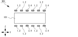
- Fig. 19 is a diagram for explaining an exemplary embodiment of the light emitting module 901.
- Fig. 19 is a schematic diagram of the light emitting module 901.
- the light-emitting module 901 includes a plurality of light-emitting devices 1 or 2, a plurality of light-emitting devices 3 or 4, and a light guide plate 101.
- the plurality of light-emitting devices 1 or 2 includes a case where the plurality of light-emitting devices 1 or 2 is composed of a plurality of light-emitting devices 1, a case where the plurality of light-emitting devices 2 is composed of one or more light-emitting devices 1 and one or more light-emitting devices 2.
- the plurality of light-emitting devices 3 or 4 includes a case where the plurality of light-emitting devices 3 or 4 is composed of a plurality of light-emitting devices 3, a case where the plurality of light-emitting devices 4 is composed of one or more light-emitting devices 3 and one or more light-emitting devices 4.
- the plurality of light-emitting devices 1 or 2 will be referred to as a plurality of first light-emitting devices
- the plurality of light-emitting devices 3 or 4 will be referred to as a plurality of second light-emitting devices.
- Figs. 1 to 18 are also diagrams for explaining the light emitting module 901.
- the color of light emitted from the first light emitting device is different from the color of light emitted from the second light emitting device.
- the emission peak wavelength of the light emitted from the first light emitting device is different from the emission peak wavelength of the light emitted from the second light emitting device.
- the difference between the emission peak wavelength of the light emitted from the first light emitting device and the emission peak wavelength of the light emitted from the second light emitting device is at least 20 nm or more.
- the first light emitting device does not have a wave plate.
- the second light emitting device has a wave plate 70.
- the polarization direction of the light emitted from the semiconductor laser element 20 (hereinafter referred to as the first semiconductor laser element) of the first light emitting device is different from the polarization direction of the light emitted from the semiconductor laser element 20 (hereinafter referred to as the second semiconductor laser element) of the second light emitting device.
- the multiple first light-emitting devices and multiple second light-emitting devices include one or more first light-emitting devices and one or more second light-emitting devices that emit light in the same direction.
- Emitting light in the same direction here means that the fast axis directions of the light are also the same, and the slow axis directions are also the same.
- Each of the one or more first light-emitting devices and the one or more second light-emitting devices emits light from the top surface 14A whose fast axis direction is parallel to the first direction and whose slow axis direction is parallel to the second direction.
- the polarization direction of the light emitted from each of the one or more first light-emitting devices and the one or more second light-emitting devices is the same.
- the wave plate 70 provided in the second light-emitting device changes the polarization direction of the light emitted from the second semiconductor laser element, and emits light with the same polarization direction as the light emitted from the first light-emitting device. This makes it possible to align the polarization direction of the light emitted from the one or more first light-emitting devices and the one or more second light-emitting devices.
- the plurality of first light-emitting devices includes two first light-emitting devices that emit light of different colors.
- the plurality of first light-emitting devices includes two first light-emitting devices that emit light of different emission peak wavelengths. The difference between the emission peak wavelengths of these two first light-emitting devices is at least 20 nm or more.
- the plurality of first light-emitting devices and the plurality of second light-emitting devices include a light-emitting device having a semiconductor laser element 20 that emits red light, a light-emitting device having a semiconductor laser element 20 that emits green light, and a light-emitting device having a semiconductor laser element 20 that emits blue light.
- the plurality of first light-emitting devices include a light-emitting device having a semiconductor laser element 20 that emits green light, and a light-emitting device having a semiconductor laser element 20 that emits blue light
- the plurality of second light-emitting devices include a light-emitting device having a semiconductor laser element 20 that emits red light.
- the light emitting module 901 may be configured with a second light emitting device having a semiconductor laser element 20 that emits red light, a first light emitting device having a semiconductor laser element 20 that emits green light, and a second light emitting device having a semiconductor laser element 20 that emits blue light. In other words, the light emitting module 901 may be configured with one or more second light emitting devices, rather than multiple second light emitting devices.
- the light emitting module 901 may be configured with a first light emitting device having a semiconductor laser element 20 that emits red light, a second light emitting device having a semiconductor laser element 20 that emits green light, and a third light emitting device having a semiconductor laser element 20 that emits blue light.
- the light emitting module 901 may include one or more first light emitting devices, rather than multiple first light emitting devices.
- the light emitting module 901 may include one or more first light emitting devices and one or more second light emitting devices, and the one or more first light emitting devices and the one or more second light emitting devices may include a light emitting device having a semiconductor laser element 20 that emits red light, a light emitting device having a semiconductor laser element 20 that emits green light, and a light emitting device having a semiconductor laser element 20 that emits blue light.
- One or more first light-emitting devices and one or more second light-emitting devices that emit light in the same direction are arranged side by side in the first direction. Since the one or more first light-emitting devices and the one or more second light-emitting devices emit light that is diffused in the first direction by the lens surface 14M, the distance between the light-emitting devices can be determined based on the diffused light.
- the light emitted from the multiple first light-emitting devices and the multiple second light-emitting devices enters the light guide plate 101.
- the light emitted from the first light-emitting devices and the light emitted from the second light-emitting devices enter the light guide plate 101 with their polarization directions aligned.
- the distance between the first light-emitting devices and the second light-emitting devices arranged side by side in the first direction can be increased, and the number of light-emitting devices included in the light-emitting module 901 can be reduced.
- FIGS. 1, 2, 9 to 13, and 20 to 21C are drawings for explaining an exemplary embodiment of the light emitting device 6.
- FIG. 1 is a perspective view of the light emitting device 6.
- FIG. 2 is a side view of the light emitting device 6.
- FIG. 9 is a perspective view showing the structure inside the package of the light emitting device 6.
- FIG. 10 is a top view showing the structure inside the package of the light emitting device 6.
- FIG. 11 is a bottom view of the package 10.
- FIG. 12 is a top view showing the arrangement of the semiconductor laser element 20 and the submount 30.
- FIG. 13 is a side view showing the arrangement of the semiconductor laser element 20 and the submount 30.
- FIG. 1 is a perspective view of the light emitting device 6.
- FIG. 2 is a side view of the light emitting device 6.
- FIG. 9 is a perspective view showing the structure inside the package of the light emitting device 6.
- FIG. 10 is a top view showing the structure inside the package of the light emitting device 6.
- FIG. 20 is a cross-sectional view of the light emitting device 6. Note that the wiring 60 is omitted in the cross-sectional view of FIG. 20.
- the cross-sectional position of the cross-sectional view of the light emitting device 6 in FIG. 20 corresponds to the cross-sectional view of the light emitting device 1 in FIG. 3.
- FIG. 21A is a diagram showing the light intensity distribution of the first light in a virtual plane that is a predetermined distance away from the light emitting device 6 in the fast axis direction.
- Fig. 21B is a diagram showing a light intensity distribution of the second light in a virtual plane a predetermined distance away from the light-emitting device 6 in the fast-axis direction.
- Fig. 21C is a diagram showing a light intensity distribution of the combined light of the first light and the second light in a virtual plane a predetermined distance away from the light-emitting device 6 in the fast-axis direction.
- the light emitting device 6 has a number of components. These components include a package 10B, one or more semiconductor laser elements 20, one or more submounts 30, one or more reflecting members 40, one or more protective elements 50, and a number of wirings 60.
- the package 10B has two or more lens surfaces 14M.
- the two or more lens surfaces 14M include a first lens surface 14M1 and a second lens surface 14M2.
- the two or more lens surfaces 14M are formed in a continuous manner.
- the two or more lens surfaces 14M each have the same shape.
- Light-emitting device 6 In light emitting device 6, light emitted from one semiconductor laser element 20 is incident on two or more lens surfaces 14M. Light emitted from one semiconductor laser element 20 is incident on first lens surface 14M1 and second lens surface 14M2.
- the light emitted from one semiconductor laser element 20 and incident on the first lens surface 14M1 is referred to as the first light.
- the light emitted from one semiconductor laser element 20 and incident on the second lens surface 14M2 is referred to as the second light.
- the light emitted from one semiconductor laser element 20 can be said to be a combination of the first light and the second light.
- the cover 14 emits light from the top surface 14A, the light intensity distribution of the light emitted from the semiconductor laser element 20 in the fast axis direction being more uniform than the light emitted from the semiconductor laser element 20.
- Light is emitted from the light emitting device 6 so that the light intensity distribution in a virtual plane a predetermined distance away from the light emitting device 6 in the fast axis direction is more uniform than the light intensity distribution in the FFP of the light emitted from the semiconductor laser element 20.
- the light of peak light intensity in the first light and the light of peak light intensity in the second light are located at both ends of the irradiation area in this virtual plane.
- the first light has a light intensity distribution on first lens surface 14M1 such that the light intensity decreases in the direction from second lens surface 14M2 to first lens surface 14M1.
- the first light has a light intensity distribution such that the light intensity increases in the direction from second lens surface 14M2 to first lens surface 14M1 (see FIG. 21A).
- the second light has a light intensity distribution on second lens surface 14M2 such that the light intensity decreases in the direction from first lens surface 14M1 to second lens surface 14M2.
- the second light has a light intensity distribution such that the light intensity increases in the direction from first lens surface 14M1 to second lens surface 14M2 (see FIG. 21B).
- the first light and the second light overlap on a virtual plane that is a specified distance away, achieving a more uniform light intensity distribution (see Figure 21C).
- FIGS. 1, 2, 7, 8, 11 to 13, and 22 are drawings for explaining an exemplary embodiment of the light emitting device 7.
- FIG. 1 is a perspective view of the light emitting device 7.
- FIG. 2 is a side view of the light emitting device 7.
- FIG. 7 is a perspective view of the lid 14 from the side where the lens surface 14M is provided.
- FIG. 8 is a top view of the lid 14 from the side where the lens surface is provided.
- FIGS. 1 is a perspective view of the light emitting device 7.
- FIG. 2 is a side view of the light emitting device 7.
- FIG. 7 is a perspective view of the lid 14 from the side where the lens surface 14M is provided.
- FIG. 8 is a top view of the lid 14 from the side where the lens surface is provided.
- FIGS. 1 is a perspective view of the light emitting device 7.
- FIG. 2 is a side view of the light emitting device 7.
- FIG. 7 is a perspective view of the lid 14 from the side where the lens surface 14M
- FIG. 11 is a bottom view of the package 10.
- FIG. 12 is a top view showing the arrangement of the semiconductor laser element 20 and the submount 30.
- FIG. 13 is a side view showing the arrangement of the semiconductor laser element 20 and the submount 30.
- FIG. 22 is a cross-sectional view of the light emitting device 7. In addition, in the cross-sectional view of FIG. 22, the wiring 60 is omitted. 22 of the light emitting device 7 corresponds to the cross-sectional view of the light emitting device 1 in FIG.
- the light emitting device 7 has a number of components. These components include a package 10, one or more semiconductor laser elements 20, one or more submounts 30, one or more reflecting members 40A, one or more protective elements 50, and a number of wirings 60.
- the reflecting member 40A has two or more light reflecting surfaces 41B.
- the two or more light reflecting surfaces 41B include a first light reflecting surface 41B1 and a second light reflecting surface 41B2.
- the two or more light reflecting surfaces 41B are provided in a continuous manner.
- Light emitting device 7 In the light emitting device 7, light emitted from one semiconductor laser element 20 is incident on two or more light reflecting surfaces 41B. Light emitted from one semiconductor laser element 20 is incident on the first light reflecting surface 41B1 and the second light reflecting surface 41B2.
- the light emitted from one semiconductor laser element 20 and incident on the first light reflecting surface 41B1 is referred to as the first reflected light.
- the light emitted from one semiconductor laser element 20 and incident on the second light reflecting surface 41B2 is referred to as the second reflected light.
- the light emitted from one semiconductor laser element 20 can be said to be a combination of the first reflected light and the second reflected light.
- the reflecting member 40A makes the light intensity distribution in the fast axis direction of the light emitted from the semiconductor laser element 20 more uniform than the light emitted from the semiconductor laser element 20, and causes the light to be incident on the lens surface 14M.
- Light is emitted from the light emitting device 7 so that the light intensity distribution in a virtual plane a predetermined distance away from the light emitting device 7 in the fast axis direction is more uniform than the light intensity distribution in the FFP of the light emitted from the semiconductor laser element 20.
- the reflecting member 40A optically controls the light emitted from the semiconductor laser element 20 so that the light intensity distribution is more uniform
- the lens surface 14M optically controls the light emitted from the semiconductor laser element 20 so that the spread of the light is increased.
- Optical control that makes the light intensity distribution at a specified distance more uniform by using two or more light reflecting surfaces 41B can be achieved by citing the optical control described in Japanese Patent Application No. 2017-157063 and Japanese Patent Application No. 2018-13695.
- these applications aim to make the light intensity distribution uniform on the lower or upper surface of the fluorescent part, but the light emitting device 6 differs in that the light intensity distribution is made more uniform on a virtual plane a specified distance away from the light emitting device 6.
- the only difference is the position (optical path length) where the light intensity distribution is made more uniform, and the principle of optical control is the same.
- the two or more lens surfaces 14M of the lid 14 achieve both the effect of increasing the spread of light in the fast axis direction and the effect of making the light intensity distribution in the fast axis direction more uniform, but in the light-emitting device 7, these effects are shared between the reflecting member 40A and the lid 14, increasing the spread of light in the fast axis direction and emitting light with a more uniform light intensity distribution in the fast axis direction from the light-emitting device 7.
- This allows the positions of the two components to be adjusted for implementation, so that the implementation position of one component can be adjusted to take into account the misalignment of the other component.
- the light emitting device and light emitting module of the present invention are not strictly limited to the light emitting device and light emitting module of each embodiment.
- the present invention can be realized without being limited to the external shape and structure of the light emitting device and light emitting module disclosed in each embodiment.
- the present invention can be applied without necessarily including all components. For example, if some of the components of the light emitting device disclosed in the embodiment are not described in the claims, the freedom of design by those skilled in the art, such as substitution, omission, modification of shape, and change of material, is recognized for some of the components, and the invention described in the claims is specified to be applied.
- a base having a base portion having a first upper surface and a frame portion having a second upper surface; a semiconductor laser element disposed on the first upper surface and emitting light having an elliptical far-field pattern; a lid having an upper surface, a lower surface bonded to the second upper surface, and a cylindrical lens surface formed on the lower surface side so as to be recessed toward the upper surface; Equipped with the semiconductor laser element is disposed in a sealed space surrounded by the base body and the lid body, The lid further diffuses the fast axis direction of light emitted from the semiconductor laser element and incident on the cylindrical lens surface, causing the light to exit from the top surface.
- Item 2 2.
- the light emitting device wherein the lid body emits light from the top surface, the light intensity distribution of the light emitted from the semiconductor laser element in a fast axis direction being more uniform than that of the light emitted from the semiconductor laser element.
- a reflecting member arranged at a position away from the semiconductor laser element in a first direction and configured to reflect light emitted from the semiconductor laser element;
- the lid body has one or more inner surfaces connected to the lower surface and the cylindrical lens surface, 3.
- the light emitting device according to item 1 or 2, wherein the one or more inner surfaces include an inner surface that overlaps with the second upper surface in a top view. (Item 4) 4.
- the light emitting device makes the light intensity distribution in the fast axis direction of the light emitted from the semiconductor laser element more uniform than the light emitted from the semiconductor laser element and causes the light to be incident on the cylindrical lens surface.
- the light emitting device according to item 3 or 4, wherein light along an optical axis emitted from the semiconductor laser element is reflected by the reflecting member in a direction perpendicular to the first upper surface.
- an outer edge shape of the base is a rectangle whose width in the first direction is greater than its width in a second direction perpendicular to the first direction when viewed from above.
- Item 7 7.
- the light emitting device according to any one of claims 1 to 6, wherein a divergence angle in the fast axis direction of the light emitted from the lid is 1.1 to 2.5 times a divergence angle in the fast axis direction of the light emitted from the semiconductor laser element.
- the frame portion of the base further has a plurality of inner surfaces intersecting with the second upper surface, 8.
- the light emitting device according to any one of items 1 to 9, wherein the cylindrical lens surface is a lens surface on which a point passing through an optical axis of the lens is located at the top. (Item 11) Item 11. The light emitting device according to any one of items 1 to 10, wherein light is emitted such that the light intensity distribution in a virtual plane a predetermined distance away from the light emitting device in the fast axis direction is more uniform than the light intensity distribution in the FFP of the light emitted from the semiconductor laser element.
- Item 1 is a light emitting device according to the present invention, comprising: a first light emitting device not including a wave plate; A second light emitting device which is the light emitting device according to item 9; a light guide plate into which the light emitted from the first light emitting device and the light emitted from the second light emitting device are incident with their polarization directions aligned; A light emitting module comprising:
- the light-emitting device and light-emitting module described in the embodiments can be used as backlights for head-mounted displays and other displays.
- the display field can be said to be one application form to which the present invention can be applied.
- the present invention is not limited to this, and can be used in various applications such as projectors, lighting, exposure, and vehicle headlights.
Landscapes
- Physics & Mathematics (AREA)
- Condensed Matter Physics & Semiconductors (AREA)
- General Physics & Mathematics (AREA)
- Electromagnetism (AREA)
- Optics & Photonics (AREA)
- Semiconductor Lasers (AREA)
Priority Applications (1)
| Application Number | Priority Date | Filing Date | Title |
|---|---|---|---|
| JP2025530104A JPWO2025005019A1 (https=) | 2023-06-28 | 2024-06-21 |
Applications Claiming Priority (2)
| Application Number | Priority Date | Filing Date | Title |
|---|---|---|---|
| JP2023-106250 | 2023-06-28 | ||
| JP2023106250 | 2023-06-28 |
Publications (1)
| Publication Number | Publication Date |
|---|---|
| WO2025005019A1 true WO2025005019A1 (ja) | 2025-01-02 |
Family
ID=93938539
Family Applications (1)
| Application Number | Title | Priority Date | Filing Date |
|---|---|---|---|
| PCT/JP2024/022676 Ceased WO2025005019A1 (ja) | 2023-06-28 | 2024-06-21 | 発光装置、及び、発光モジュール |
Country Status (3)
| Country | Link |
|---|---|
| JP (1) | JPWO2025005019A1 (https=) |
| TW (1) | TW202520593A (https=) |
| WO (1) | WO2025005019A1 (https=) |
Citations (10)
| Publication number | Priority date | Publication date | Assignee | Title |
|---|---|---|---|---|
| JP2002277781A (ja) * | 2000-12-21 | 2002-09-25 | Xerox Corp | 複数ビーム式ラスタ出力スキャニングシステム |
| JP2015233053A (ja) * | 2014-06-09 | 2015-12-24 | 三菱電機株式会社 | 半導体レーザー装置 |
| WO2017007024A1 (ja) * | 2015-07-08 | 2017-01-12 | 国立大学法人香川大学 | 分光測定装置 |
| JP2017069241A (ja) * | 2015-09-28 | 2017-04-06 | 京セラ株式会社 | 半導体レーザ素子用パッケージおよび半導体レーザ装置 |
| JP2019028450A (ja) * | 2017-07-31 | 2019-02-21 | 三星電子株式会社Samsung Electronics Co.,Ltd. | メタプロジェクタ、及びそれを含む電子装置 |
| JP2019036638A (ja) * | 2017-08-16 | 2019-03-07 | 日亜化学工業株式会社 | 発光装置 |
| JP2020053535A (ja) * | 2018-09-26 | 2020-04-02 | 日亜化学工業株式会社 | 光源装置とその製造方法 |
| JP2021025964A (ja) * | 2019-08-08 | 2021-02-22 | 富士ゼロックス株式会社 | 発光装置、光学装置及び情報処理装置 |
| US20210185190A1 (en) * | 2016-06-27 | 2021-06-17 | Intel Corporation | Compact, low cost vcsel projector for high performance stereodepth camera |
| JP2023043376A (ja) * | 2021-09-16 | 2023-03-29 | 日亜化学工業株式会社 | 発光装置およびバックライト |
-
2024
- 2024-06-21 JP JP2025530104A patent/JPWO2025005019A1/ja active Pending
- 2024-06-21 WO PCT/JP2024/022676 patent/WO2025005019A1/ja not_active Ceased
- 2024-06-25 TW TW113123515A patent/TW202520593A/zh unknown
Patent Citations (10)
| Publication number | Priority date | Publication date | Assignee | Title |
|---|---|---|---|---|
| JP2002277781A (ja) * | 2000-12-21 | 2002-09-25 | Xerox Corp | 複数ビーム式ラスタ出力スキャニングシステム |
| JP2015233053A (ja) * | 2014-06-09 | 2015-12-24 | 三菱電機株式会社 | 半導体レーザー装置 |
| WO2017007024A1 (ja) * | 2015-07-08 | 2017-01-12 | 国立大学法人香川大学 | 分光測定装置 |
| JP2017069241A (ja) * | 2015-09-28 | 2017-04-06 | 京セラ株式会社 | 半導体レーザ素子用パッケージおよび半導体レーザ装置 |
| US20210185190A1 (en) * | 2016-06-27 | 2021-06-17 | Intel Corporation | Compact, low cost vcsel projector for high performance stereodepth camera |
| JP2019028450A (ja) * | 2017-07-31 | 2019-02-21 | 三星電子株式会社Samsung Electronics Co.,Ltd. | メタプロジェクタ、及びそれを含む電子装置 |
| JP2019036638A (ja) * | 2017-08-16 | 2019-03-07 | 日亜化学工業株式会社 | 発光装置 |
| JP2020053535A (ja) * | 2018-09-26 | 2020-04-02 | 日亜化学工業株式会社 | 光源装置とその製造方法 |
| JP2021025964A (ja) * | 2019-08-08 | 2021-02-22 | 富士ゼロックス株式会社 | 発光装置、光学装置及び情報処理装置 |
| JP2023043376A (ja) * | 2021-09-16 | 2023-03-29 | 日亜化学工業株式会社 | 発光装置およびバックライト |
Also Published As
| Publication number | Publication date |
|---|---|
| TW202520593A (zh) | 2025-05-16 |
| JPWO2025005019A1 (https=) | 2025-01-02 |
Similar Documents
| Publication | Publication Date | Title |
|---|---|---|
| US20260095020A1 (en) | Light-emitting module | |
| JP2025120354A (ja) | 発光装置 | |
| US12342666B2 (en) | Light-emitting device | |
| WO2025005019A1 (ja) | 発光装置、及び、発光モジュール | |
| JP2025007840A (ja) | 発光装置、発光モジュール、及び、発光装置の製造方法 | |
| JP7747963B2 (ja) | 発光モジュール | |
| JP2025052848A (ja) | 複数の発光装置及び複数の発光装置の製造方法 | |
| JP2025099985A (ja) | 発光装置、発光モジュール、及び、複数の発光装置 | |
| US20250133884A1 (en) | Light-emitting device | |
| JP2026042707A (ja) | 発光装置 | |
| EP4704267A2 (en) | Light-emitting device | |
| JP2024172656A (ja) | 発光モジュール、実装基板、及び、実装基板の製造方法 | |
| WO2025115270A1 (ja) | 発光装置、及び、発光モジュール | |
| JP2026057166A (ja) | 発光装置 | |
| WO2024247467A1 (ja) | 発光装置 | |
| US20250087964A1 (en) | Manufacturing method of mounting substrate, mounting substrate, and light-emitting module | |
| US20260106433A1 (en) | Light emitting device and light emitting module | |
| US20230352902A1 (en) | Light-emitting device and light-emitting module | |
| JP2025170122A (ja) | 発光モジュール | |
| WO2025088915A1 (ja) | 基体、発光装置、及び、発光モジュール | |
| WO2025225606A1 (ja) | 基体、発光装置、及び、発光モジュール | |
| WO2024085205A1 (ja) | 発光装置 | |
| CN121939218A (zh) | 发光装置 | |
| JP2025043316A (ja) | 発光装置、及び、発光装置の製造方法 | |
| JP2026071147A (ja) | 発光装置及び発光モジュール |
Legal Events
| Date | Code | Title | Description |
|---|---|---|---|
| 121 | Ep: the epo has been informed by wipo that ep was designated in this application |
Ref document number: 24831880 Country of ref document: EP Kind code of ref document: A1 |
|
| ENP | Entry into the national phase |
Ref document number: 2025530104 Country of ref document: JP Kind code of ref document: A |
|
| WWE | Wipo information: entry into national phase |
Ref document number: 2025530104 Country of ref document: JP |
|
| NENP | Non-entry into the national phase |
Ref country code: DE |