WO2025004914A1 - 有機エレクトロルミネッセンス表示装置 - Google Patents
有機エレクトロルミネッセンス表示装置 Download PDFInfo
- Publication number
- WO2025004914A1 WO2025004914A1 PCT/JP2024/022151 JP2024022151W WO2025004914A1 WO 2025004914 A1 WO2025004914 A1 WO 2025004914A1 JP 2024022151 W JP2024022151 W JP 2024022151W WO 2025004914 A1 WO2025004914 A1 WO 2025004914A1
- Authority
- WO
- WIPO (PCT)
- Prior art keywords
- optically anisotropic
- anisotropic layer
- layer
- organic
- film
- Prior art date
- Legal status (The legal status is an assumption and is not a legal conclusion. Google has not performed a legal analysis and makes no representation as to the accuracy of the status listed.)
- Ceased
Links
Images


Classifications
-
- H—ELECTRICITY
- H10—SEMICONDUCTOR DEVICES; ELECTRIC SOLID-STATE DEVICES NOT OTHERWISE PROVIDED FOR
- H10K—ORGANIC ELECTRIC SOLID-STATE DEVICES
- H10K59/00—Integrated devices, or assemblies of multiple devices, comprising at least one organic light-emitting element covered by group H10K50/00
- H10K59/80—Constructional details
- H10K59/8793—Arrangements for polarized light emission
-
- G—PHYSICS
- G02—OPTICS
- G02B—OPTICAL ELEMENTS, SYSTEMS OR APPARATUS
- G02B5/00—Optical elements other than lenses
- G02B5/30—Polarising elements
-
- G—PHYSICS
- G09—EDUCATION; CRYPTOGRAPHY; DISPLAY; ADVERTISING; SEALS
- G09F—DISPLAYING; ADVERTISING; SIGNS; LABELS OR NAME-PLATES; SEALS
- G09F9/00—Indicating arrangements for variable information in which the information is built-up on a support by selection or combination of individual elements
-
- G—PHYSICS
- G09—EDUCATION; CRYPTOGRAPHY; DISPLAY; ADVERTISING; SEALS
- G09F—DISPLAYING; ADVERTISING; SIGNS; LABELS OR NAME-PLATES; SEALS
- G09F9/00—Indicating arrangements for variable information in which the information is built-up on a support by selection or combination of individual elements
- G09F9/30—Indicating arrangements for variable information in which the information is built-up on a support by selection or combination of individual elements in which the desired character or characters are formed by combining individual elements
-
- H—ELECTRICITY
- H10—SEMICONDUCTOR DEVICES; ELECTRIC SOLID-STATE DEVICES NOT OTHERWISE PROVIDED FOR
- H10K—ORGANIC ELECTRIC SOLID-STATE DEVICES
- H10K50/00—Organic light-emitting devices
- H10K50/80—Constructional details
- H10K50/86—Arrangements for improving contrast, e.g. preventing reflection of ambient light
-
- H—ELECTRICITY
- H10—SEMICONDUCTOR DEVICES; ELECTRIC SOLID-STATE DEVICES NOT OTHERWISE PROVIDED FOR
- H10K—ORGANIC ELECTRIC SOLID-STATE DEVICES
- H10K59/00—Integrated devices, or assemblies of multiple devices, comprising at least one organic light-emitting element covered by group H10K50/00
- H10K59/10—OLED displays
-
- H—ELECTRICITY
- H10—SEMICONDUCTOR DEVICES; ELECTRIC SOLID-STATE DEVICES NOT OTHERWISE PROVIDED FOR
- H10K—ORGANIC ELECTRIC SOLID-STATE DEVICES
- H10K59/00—Integrated devices, or assemblies of multiple devices, comprising at least one organic light-emitting element covered by group H10K50/00
- H10K59/80—Constructional details
- H10K59/8791—Arrangements for improving contrast, e.g. preventing reflection of ambient light
Definitions
- Figure 2 is a diagram showing the relationship between the absorption axis of the polarizer 22 and the in-plane slow axis of the optically anisotropic layer 24 in the organic EL display device 10 shown in Figure 1.
- the absorption axis of the polarizer 22 is parallel to the y-axis direction, and the angle between the in-plane slow axis of the optically anisotropic layer 24 and the y-axis direction is 45°.
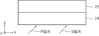
- Figure 3 shows a mode in which light is obliquely incident from the side opposite to the polarizer 22 side of the optically anisotropic layer 24.
- the light is divided into P-polarized light and S-polarized light, and the vibration directions are indicated by the black arrow and white arrow shown in Figure 2.
- the polarization state changes.
- y which is the ratio of the in-plane retardation at a wavelength of 600 nm to the in-plane retardation at a wavelength of 440 nm of the optically anisotropic layer 24
- the incident P polarized light and S polarized light are brought into a polarization state in which they have different absorptances with respect to the absorption axis of the polarizer 22.
- the P polarized light is brought into a polarization state in which it is difficult to be absorbed by the polarizer 22.
- the organic EL display device 10 is rotated 45° to set the relationship between the absorption axis of the polarizer 22 and the in-plane slow axis of the optically anisotropic layer 24 as shown in Fig. 4.
- light is obliquely incident from the side opposite to the polarizer 22 side of the optically anisotropic layer 24, as in Fig. 3.
- the light is divided into P-polarized light and S-polarized light, and the vibration directions are indicated by the black arrow and the white arrow shown in Fig. 4.
- the absorption of P-polarized light is suppressed more than in the embodiment shown in Fig. 5, and as a result, the brightness of the transmitted light passing through the polarizer 22 is greater in the embodiment shown in Fig. 3. Therefore, the color appears different depending on the azimuth angle at which the organic EL display device 10 is viewed. As described above, it has been found that the values of x and y described later may cause the above-mentioned difference in brightness depending on the azimuth angle.
- the organic EL display device 10 since requirements 1 and 2 are satisfied, the change in the amount of P-polarized and S-polarized light transmitted through the circular polarizer due to wavelength and azimuth angle can be suppressed, and it is considered that the change in oblique color (white) at each azimuth angle is reduced.
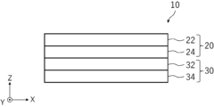
- the organic EL display device 10 since the organic EL display device 10 includes the circular polarizer 20, it also has excellent external light reflectivity. Each component of the organic EL display device 10 will be described in detail below.
- the organic EL display device 10 includes a circular polarizer 20 .
- the circularly polarizing plate 20 includes, from the organic EL display element 30 side, an optically anisotropic layer 24 and a polarizer 22 .
- the polarizer 22 may be any member having a function of converting natural light into a specific linearly polarized light, and may be, for example, an absorptive polarizer.
- Examples of the polarizer 22 include an iodine-based polarizer, a dye-based polarizer using a dichroic material, and a polyene-based polarizer.
- the iodine-based polarizer and the dye-based polarizer are produced by, for example, adsorbing iodine or a dichroic dye to polyvinyl alcohol and stretching the resulting material.
- a protective film may be disposed on one or both sides of the polarizer 22 .
- the thickness of the polarizer 22 is not particularly limited, but is preferably 35 ⁇ m or less, and more preferably 1 to 25 ⁇ m, in terms of ease of handling and excellent optical properties. The above thickness allows for the thinning of organic EL display devices.
- the optically anisotropic layer 24 is preferably a ⁇ /4 plate.
- the optically anisotropic layer 24 is preferably a ⁇ /4 plate having a single layer structure, but the embodiment is not limited as long as it is an optically anisotropic layer that can constitute a circular polarizing plate.
- the optically anisotropic layer may be a broadband ⁇ /4 plate that is a laminate of a ⁇ /2 plate and a ⁇ /4 plate.
- the ⁇ /4 plate is a plate that has the function of converting linearly polarized light of a certain wavelength into circularly polarized light (or circularly polarized light into linearly polarized light), and has Re( ⁇ ) that satisfies ⁇ /4.
- the optically anisotropic layer 24 is preferably a positive A plate.
- the angle between the in-plane slow axis of the optically anisotropic layer 24 and the absorption axis of the polarizer 22 is preferably from 35 to 55°, more preferably from 40 to 50°, and even more preferably 45°.
- the Re(550) of the optically anisotropic layer 24 is not particularly limited, but is preferably from 110 to 160 nm, and more preferably from 110 to 150 nm.
- the optically anisotropic layer 24 may have either normal wavelength dispersion or reverse wavelength dispersion. Among them, reverse wavelength dispersion is preferable. The reverse wavelength dispersion is preferably exhibited in the visible light region.
- the thickness of the optically anisotropic layer 24 is preferably from 1 to 10 ⁇ m, and more preferably from 1 to 5 ⁇ m.
- the thickness of the optically anisotropic layer 24 refers to the average thickness of the optically anisotropic layer 24.
- the average thickness is determined by measuring the thicknesses of the optically anisotropic layer 24 at any five or more points and calculating the arithmetic average.
- a specific value of the thickness of a layer is shown, it is the arithmetic average value of thicknesses measured at any five or more points of a certain layer, as described above.
- the optically anisotropic layer 24 can be produced, for example, by horizontally aligning a rod-shaped polymerizable liquid crystal compound, for example, by the method for producing a positive A plate disclosed in JP-A-2008-225281 and JP-A-2008-026730.
- a method for producing an optically anisotropic layer with reverse wavelength dispersion a method of obtaining the layer by horizontally aligning a liquid crystal compound with reverse wavelength dispersion can be mentioned.
- the term "reverse wavelength dispersion" liquid crystal compound refers to a compound in which, when the in-plane retardation (Re) value in the visible light range of the optically anisotropic layer produced using the compound is measured, the Re value becomes equal or higher as the measured wavelength increases.
- liquid crystal compounds with reverse wavelength dispersion examples include compounds represented by general formula (I) described in JP-A-2008-297210 (particularly, the compounds described in paragraphs [0034] to [0039]), compounds represented by general formula (1) described in JP-A-2010-084032 (particularly, the compounds described in paragraphs [0067] to [0073]), and compounds represented by general formula (1) described in JP-A-2016-081035 (particularly, the compounds described in paragraphs [0043] to [0055]).
- the organic EL display element 30 is a display element having a pair of electrodes and an organic light-emitting layer sandwiched between the electrodes.
- layers such as a hole injection layer, a hole transport layer, an electron injection layer, an electron transport layer, and a protective layer may be provided between the electrodes of the organic EL display element 30, and each of these layers may have other functions.
- Various materials can be used to form each layer.
- the organic EL display element 30 includes a polarization adjustment layer 32 and an organic EL substrate 34 .
- the polarization adjustment layer 32 is a layer that adjusts the amount of P-polarized light and S-polarized light transmitted through the polarization adjustment layer 32, and is a layer that can mainly make the amount of P-polarized light transmitted greater than the amount of S-polarized light transmitted.
- the polarization adjustment layer 32 preferably includes an alternating layer in which high refractive index layers and low refractive index layers are alternately stacked in this order, and a depolarizing layer, and the depolarizing layer is preferably disposed on the organic EL substrate 34 side.
- the light emitted from the organic EL substrate 34 (particularly, the light emitted in an oblique direction) first loses its polarization state when passing through the depolarizing layer, and becomes light with an equal ratio of P-polarized light and S-polarized light.
- the ratio of P-polarized light and S-polarized light in the light that passes through the alternating layer can be controlled by controlling the number of interfaces.
- the alternating layer is a layer in which high refractive index layers and low refractive index layers are alternately laminated, specifically, a layer consisting of a high refractive index layer, a low refractive index layer, a high refractive index layer, and a low refractive index layer, and so on, in that order. It is preferable that the high refractive index layer and the low refractive index layer are arranged so as to be in contact with each other. In other words, it is preferable that there is no other layer between the high refractive index layer and the low refractive index layer.
- the number of high refractive index layers in a layer in which high refractive index layers and low refractive index layers are alternately laminated is preferably 1 to 10, more preferably 1 to 5, even more preferably 1 to 3, and particularly preferably 1 or 2, from the viewpoint of oblique color.
- the number of stacked high refractive index layers is preferably one more than the number of stacked low refractive index layers.
- the number of stacked high refractive index layers is one more than the number of stacked low refractive index layers.
- the refractive index of the high refractive index layer at a wavelength of 550 nm is preferably from 1.7 to 2.7, and more preferably from 1.9 to 2.3.
- the material constituting the high refractive index layer is not particularly limited, and known materials are used.
- the high refractive index layer may be an inorganic film or an organic film, and is preferably an inorganic film.
- the material constituting the inorganic film is preferably silicon nitride.
- the high refractive index layer is preferably a layer containing silicon nitride (hereinafter, also referred to as a "silicon nitride layer").
- the silicon nitride layer preferably contains silicon atoms and nitrogen atoms, and may also contain oxygen atoms or hydrogen atoms.
- the composition ratio of nitrogen atoms and silicon atoms in the silicon nitride layer is preferably 1.0 to 2.0, and more preferably 1.2 to 1.4.
- the silicon nitride layer may contain other inorganic substances in addition to silicon nitride.
- the content of silicon nitride is preferably from 90 to 100 mass %, and more preferably from 99 to 100 mass %, based on the total mass of the silicon nitride layer.
- the thickness of the silicon nitride layer is preferably 10 nm or more, more preferably 20 nm or more, and is preferably 150 nm or less, more preferably 80 nm or less.
- the thickness of the silicon nitride layer is the thickness of a single film, not the total thickness of a plurality of silicon nitride layers.
- Methods for forming a silicon nitride layer include, for example, sputtering, vacuum deposition, ion plating, and plasma CVD (Chemical Vapor Deposition), and specific examples include the methods for forming a silicon nitride layer described in JP 2011-063851 A, Japanese Patent No. 3400324, JP 2002-322561 A, and JP 2002-361774 A.
- the low refractive index layer is a layer having a refractive index lower than that of the high refractive index layer.
- the refractive index of the low refractive index layer at a wavelength of 550 nm is preferably from 1.4 to 1.6, and more preferably from 1.45 to 1.55.
- the material constituting the low refractive index layer is not particularly limited, and known materials can be used.
- the low refractive index layer may be an inorganic film or an organic film, and is preferably an organic film.
- the organic layer preferably contains a known resin.
- the resin examples include epoxy resin, acrylic resin, methacrylic resin, polyester, methacrylic acid-maleic acid copolymer, polystyrene, transparent fluororesin, polyimide, fluorinated polyimide, polyamide, polyamideimide, polyetherimide, cellulose acylate, polyurethane, polyether ketone, polycarbonate, fluorene ring-modified polycarbonate, alicyclic modified polycarbonate, and fluorene ring-modified polyester, and acrylic resin or methacrylic resin is preferable.
- the thickness of the organic layer is preferably 0.3 to 10 ⁇ m.
- the thickness of the organic layer is the thickness of a single film, not the total thickness of a plurality of organic layers.
- the organic layer can be formed, for example, by applying a coating liquid containing a monomer and a polymerization initiator, etc., onto a substrate by a known coating method such as roll coating, gravure coating, or spray coating, drying the liquid, and curing it, if necessary, by heating, ultraviolet irradiation, electron beam irradiation, etc.
- a coating liquid containing a monomer and a polymerization initiator etc.
- Other examples include a flash evaporation method in which the coating liquid is evaporated, the vapor is attached to the substrate, cooled/condensed to form a liquid film, and the film is cured by ultraviolet light or electron beams, and a transfer method in which a sheet-like organic layer is transferred.
- alternating layer a layer in which silicon nitride layers and organic layers are alternately laminated in this order is preferred.
- the depolarizing layer is not particularly limited as long as it is a layer that can depolarize the light incident on the depolarizing layer, and examples thereof include a known high birefringence resin layer and a known diffusion layer.
- the high birefringence resin layer include layers containing resins such as polyethylene terephthalate, acrylic resins, methacrylic resins, and polycarbonates, which have high birefringence.
- the diffusion layer include a diffusion layer made of a diffusing agent such as a filler and a resin, and a diffusion layer including a layer containing the diffusing agent and a resin layer.
- the filler include an inorganic filler such as silicon dioxide, and an organic filler such as an acrylic resin.
- the organic EL substrate 34 may be, for example, a substrate that constitutes a known organic EL element.
- the substrate may be one having a pair of electrodes and an organic light-emitting layer sandwiched between them, as described above.
- the organic EL display device may have layers other than the above-mentioned members.
- the other layer may be, for example, an adhesive layer. It is preferable that the organic EL display device has an adhesive layer between each of the members. Examples of the adhesive layer include a known alignment film, a known pressure sensitive adhesive layer, and a known adhesive layer.
- Examples of methods for forming the alignment film include rubbing treatment of an organic compound (preferably a resin), oblique deposition of an inorganic compound, a method for forming a layer having a microgroove, and a method for accumulating an organic compound (e.g., ⁇ -tricosanoic acid, dioctadecylmethylammonium chloride, methyl stearate) by the Langmuir-Blodgett method (LB film).
- the alignment film may also be one that generates an alignment function by application of an electric field, a magnetic field, or light irradiation (preferably polarized light).
- the alignment film is preferably formed by a rubbing treatment of a polymer.
- the alignment film may be, for example, a photo-alignment film.
- the thickness of the alignment film is not particularly limited as long as it can exhibit an alignment function, but is preferably 0.01 to 5.0 ⁇ m, more preferably 0.05 to 2.0 ⁇ m, and even more preferably 0.1 to 0.5 ⁇ m.
- the alignment film may be peelable from the optically anisotropic layer described below.
- Requirements 1 and 2 The organic EL display device satisfies the first and second requirements, and preferably satisfies the third and fourth requirements.
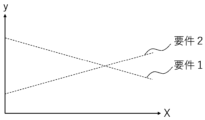
- Requirement 1 y ⁇ 0.155x+1.655
- Requirement 2 y ⁇ 0.170x+0.980
- Requirement 3 y ⁇ 0.240x+1.740
- Requirement 4 y ⁇ 0.260x+0.890
- the desired effect is achieved within the area surrounded by the dashed lines indicated as requirement 1 and the dashed lines indicated as requirement 2.
- the x value is the arithmetic average value of P/S at each azimuth angle, which is calculated when the organic EL display element displays white light in a direction where the polar angle with respect to the normal direction of the organic EL display element is 60°, at each azimuth angle rotated by 45° from the direction parallel to the transmission axis of the polarizer in the organic EL display device.
- the value of x is preferably from 1.00 to 2.00, more preferably from 1.00 to 1.70, and even more preferably from 1.00 to 1.40.
- azimuth angles are determined by rotating the direction parallel to the transmission axis of a polarizer in an organic EL display device by 45° increments.
- directions parallel to the transmission axis of a polarizer is defined as 0°
- examples of the azimuth angles include 0°, 45°, 90°, 135°, 180°, 225°, 270°, and 315°.
- the y value is the ratio of Re(600) to Re(440) in the optically anisotropic layer (Re(600)/Re(440)).
- the y value is a preferred embodiment of the above-mentioned x value, and is preferably a value that satisfies requirements 1 and 2, and more preferably a value that satisfies requirements 3 and 4.
- the y value is preferably from 1.15 to 1.50, more preferably from 1.23 to 1.45, and even more preferably from 1.30 to 1.40.
- a method for producing an optically anisotropic layer having a phase difference in the thickness direction there is a method for vertically aligning a rod-shaped polymerizable liquid crystal compound.
- a positive C plate described in JP-A-2017-187732, JP-A-2016-53709, and JP-A-2015-200861.
- the organic EL display device is not particularly limited, and any known method can be used.
- a method can be mentioned in which a composition for forming an optically anisotropic layer containing a predetermined polymerizable liquid crystal compound is applied onto a predetermined substrate to form a coating film, the coating film is then subjected to an alignment treatment, and then a curing treatment is performed to form a predetermined optically anisotropic layer, the formed optically anisotropic layer and a polarizer are laminated via an adhesion layer to prepare a circular polarizing plate, and the prepared circular polarizing plate is then bonded to an organic EL display element.
- the liquid crystal compound having a polymerizable group contained in the composition for forming an optically anisotropic layer (hereinafter also referred to as a "polymerizable liquid crystal compound”) is appropriately selected to be optimal for the formation of each optically anisotropic layer.
- the content of the polymerizable liquid crystal compound in the composition for forming an optically anisotropic layer is preferably from 60 to 99% by mass, more preferably from 70 to 98% by mass, based on the total solid content of the composition for forming an optically anisotropic layer.
- the solid content means a component capable of forming an optically anisotropic layer from which the solvent has been removed, and even if the component is in a liquid state, it is considered to be a solid content.
- the alignment treatment can be carried out by drying the coating film at room temperature or by heating the coating film.
- the liquid crystal phase formed by the alignment treatment can generally be transitioned by a change in temperature or pressure.
- the transition can also be caused by the composition ratio of the amount of solvent, etc.
- the conditions for heating the coating are not particularly limited, but the heating temperature is preferably 50 to 250° C., more preferably 50 to 150° C., and the heating time is preferably 10 seconds to 10 minutes. After the coating film is heated, the coating film may be cooled, if necessary, before the curing treatment (light irradiation treatment) described below.
- the method of hardening treatment performed on the coating film in which the polymerizable liquid crystal compound is oriented is not particularly limited, and examples thereof include light irradiation treatment and heat treatment. Among these, from the viewpoint of manufacturability, light irradiation treatment is preferred, and ultraviolet irradiation treatment is more preferred.
- the irradiation conditions for the light irradiation treatment are not particularly limited, but the amount of irradiation is preferably 50 to 1000 mJ/ cm2 .
- the atmosphere during the light irradiation treatment is not particularly limited, but a nitrogen atmosphere is preferred.
- Example 1 Preparation of Optically Anisotropic Layer C1 A polymerizable liquid crystal composition C1 having the following composition was prepared.
- Polymerizable liquid crystal composition C1 100 parts by mass of a mixture A of the following rod-shaped liquid crystal compound; 4.2 parts by mass of an acrylate monomer (A-400, manufactured by Shin-Nakamura Chemical Co., Ltd.); 2.0 parts by mass of the following polymer A; 0.8 parts by mass of the following polymer B; 1.9 parts by mass of compound A below; 5.1 parts by mass of photopolymerization initiator A below; 3.0 parts by mass of photoacid generator A below; 374 parts by mass of methyl isobutyl ketone; 94 parts by mass of ethyl propionate ------------------------------------------------------------------------------------------------------------------------------------------------------------------------------------------------------------------------------------------------------------------------------------------------------------
- the prepared polymerizable liquid crystal composition C1 was applied to a cellulose-based polymer film (TG40, manufactured by Fujifilm Corporation) as a substrate using a wire bar of #3.0, heated at 70°C for 2 minutes, and irradiated with 150 mJ/ cm2 ultraviolet light under conditions of an oxygen concentration of less than 100 ppm by volume.
- TG40 cellulose-based polymer film
- the composition was annealed at 120°C for 1 minute, and irradiated with 7.9 mJ/ cm2 (wavelength: 313 nm) UV (ultraviolet) light (ultra-high pressure mercury lamp; UL750; manufactured by HOYA) through a wire grid polarizer at room temperature to impart an alignment function, forming an optically anisotropic layer C1 with a thickness of 0.7 ⁇ m.
- the optically anisotropic layer C1 was a positive C plate.
- Polymerizable liquid crystal composition A1 was applied on the previously formed optically anisotropic layer C1 with wire bar coater #6.6 to form a composition layer.
- the formed composition layer was once heated to 120°C on a hot plate, and then cooled to 60°C to stabilize the orientation. Thereafter, the film temperature was kept at 60°C under a nitrogen atmosphere (oxygen concentration less than 100 volume ppm) using an ultra-high pressure mercury lamp, and after the first ultraviolet irradiation (80 mJ/cm 2 ), the film temperature was kept at 120°C, and the orientation was fixed by the second ultraviolet irradiation (300 mJ/cm 2 ), forming an optically anisotropic layer A1 with a thickness of 3.0 ⁇ m, and an optical laminate was produced.
- the optically anisotropic layer A1 was a positive A plate.
- the angle of the in-plane slow axis with respect to the film width direction was 45°.
- the above angle is an angle expressed as a positive value in the counterclockwise direction with the film width direction as the reference (0°) when the optically anisotropic layer A1 arranged on the optically anisotropic layer C1 is observed from the optically anisotropic layer A1 side.
- a polarizer with a protective film was prepared by the method described in Example 4 of JP-A-2021-015294, which is composed of a norbornene resin film / polarizer P1 / TAC (triacetyl cellulose) film having a hard coat layer formed on one surface.
- the optical laminate prepared above was attached to the TAC film side of the polarizer with the protective film prepared above, via the pressure-sensitive adhesive layer B described in Example 4 of JP-A-2021-015294, so that the optically anisotropic layer A1 side was the TAC film side of the polarizer with the protective film, and the angle between the absorption axis of the polarizer and the in-plane slow axis of the optically anisotropic layer A1 was 45 °. Thereafter, the cellulose-based polymer film was peeled off at the interface with the optically anisotropic layer C1 to prepare a circularly polarizing plate.
- a silicon nitride layer (silicon nitride film) was produced by the method described in Example 2 of JP 2011-063851 A in which a silicon nitride layer is formed using a CVD apparatus, to obtain a PET film with a silicon nitride layer.
- the thickness of the silicon nitride layer was 50 nm.
- composition X PMMA (15 parts by mass, weight average molecular weight: 100,000, manufactured by Sigma Aldrich, methacrylic resin) was added to tetrahydrofuran (85 parts by mass) to prepare composition X.
- a commercially available organic EL display device (Galaxy S4, manufactured by SAMSUNG) was disassembled, and the attached polarizer and retardation film were peeled off to obtain an organic EL substrate.
- the above-prepared P/S adjustment layer A was placed on the obtained organic EL substrate to prepare a panel P1.
- the P/S adjustment layer A and the organic EL substrate were bonded together via an adhesive (SK2057, manufactured by Soken Chemical Engineering Co., Ltd.) so that the PET film in the P/S adjustment layer A was in contact with the organic EL substrate.
- the optically anisotropic layer C1 in the above-prepared circular polarizer was bonded to the surface opposite to the PET film of the above-prepared P/S adjustment layer A via an adhesive (SK2057, manufactured by Soken Chemical Engineering Co., Ltd.) to prepare an organic EL display device of Example 1.
- Example 2 An organic EL display device was produced in the same manner as in Example 1, except that the optically anisotropic layer A1 was changed to an optically anisotropic layer A2 produced by the following method.
- the polymerizable liquid crystal composition A2 was applied on the optically anisotropic layer C1 prepared above with a wire bar coater #7.0 to form a composition layer.
- the formed composition layer was once heated to 120°C on a hot plate, and then cooled to 60°C to stabilize the orientation.
- the film temperature was kept at 60°C under a nitrogen atmosphere (oxygen concentration less than 100 volume ppm) using an ultra-high pressure mercury lamp, and the film was irradiated with ultraviolet light for the first time (80 mJ/cm 2 ), and then the film temperature was kept at 120°C and irradiated with ultraviolet light for the second time (300 mJ/cm 2 ) to fix the orientation, forming an optically anisotropic layer A2 with a thickness of 3.2 ⁇ m, and an optical laminate was prepared.
- the optically anisotropic layer A2 was a positive A plate.
- the angle of the in-plane slow axis with respect to the film width direction was 45°.
- the above angle is an angle expressed as a positive value in the counterclockwise direction with the film width direction as the reference (0°) when the optically anisotropic layer A2 arranged on the optically anisotropic layer C1 is observed from the optically anisotropic layer A2 side.
- Example 3 Panel P2 was produced in the same manner as in Example 1, except that P/S adjustment layer A was changed to P/S adjustment layer B consisting of five silicon nitride films (with PMMA films between the silicon nitride layers), and an organic EL display device was produced.
- Example 4 An organic EL display device was fabricated in the same manner as in Example 2, except that the panel P1 was changed to the panel P2.
- Example 5 A panel P3 was produced in the same manner as in Example 1, except that the optically anisotropic layer A1 was changed to an optically anisotropic layer A3 prepared by the method described below, and the P/S adjustment layer A was changed to a P/S adjustment layer C having three silicon nitride layers (with PMMA films between the silicon nitride layers).
- An organic EL display device was produced by using the same method as in Example 1.
- Polymerizable liquid crystal composition A3 was applied on the optically anisotropic layer C1 prepared above with a wire bar coater #6.2 to form a composition layer.
- the formed composition layer was once heated to 120°C on a hot plate, and then cooled to 60°C to stabilize the orientation.
- the film temperature was kept at 60°C under a nitrogen atmosphere (oxygen concentration less than 100 volume ppm) using an ultra-high pressure mercury lamp, and the first ultraviolet irradiation (80 mJ/cm 2 ) was performed, followed by the second ultraviolet irradiation (300 mJ/cm 2 ) with the film temperature kept at 120°C to fix the orientation, forming an optically anisotropic layer A3 with a thickness of 2.8 ⁇ m, and preparing an optical laminate.
- the optically anisotropic layer A3 was a positive A plate.
- the angle of the in-plane slow axis with respect to the film width direction was 45°.
- the above angle is an angle expressed as a positive value in the counterclockwise direction with the film width direction as the reference (0°) when the optically anisotropic layer A3 arranged on the optically anisotropic layer C1 is observed from the optically anisotropic layer A2 side.
- Example 6 An organic EL display device was fabricated in the same manner as in Example 1, except that the panel P1 was changed to the panel P3.
- Example 7 An organic EL display device was fabricated in the same manner as in Example 2, except that the panel P1 was changed to the panel P3.
- Example 8 An organic EL display device was produced in the same manner as in Example 5, except that the optically anisotropic layer A3 was changed to an optically anisotropic layer A4 produced by the following method.
- Polymerizable liquid crystal composition A4 was applied on the optically anisotropic layer C1 prepared above with wire bar coater #7.4 to form a composition layer.
- the formed composition layer was once heated to 120°C on a hot plate, and then cooled to 60°C to stabilize the orientation.
- the film temperature was kept at 60°C under a nitrogen atmosphere (oxygen concentration less than 100 volume ppm) using an ultra-high pressure mercury lamp, and after the first ultraviolet irradiation (80 mJ/cm 2 ), the film temperature was kept at 120°C, and the orientation was fixed by the second ultraviolet irradiation (300 mJ/cm 2 ), forming an optically anisotropic layer A4 with a thickness of 3.4 ⁇ m, and an optical laminate was prepared.
- the optically anisotropic layer A4 was a positive A plate.
- the angle of the in-plane slow axis with respect to the film width direction was 45°.
- the above angle is an angle expressed as a positive value in the counterclockwise direction with the film width direction as the reference (0°) when the optically anisotropic layer A4 arranged on the optically anisotropic layer C1 is observed from the optically anisotropic layer A4 side.
- Panel P4 was produced in the same manner as in Example 5, except that P/S adjustment layer A was changed to P/S adjustment layer D consisting of two silicon nitride layers (the layer between the silicon nitride layers being a PMMA film), and an organic EL display device was produced.
- Example 10 An organic EL display device was fabricated in the same manner as in Example 1, except that the panel P1 was changed to the panel P4.
- Example 11 An organic EL display device was fabricated in the same manner as in Example 8, except that the panel P3 was changed to the panel P4.
- Example 12 Preparation of photo-alignment film
- Polymer C (12.0 parts by mass) and thermal acid generator A (0.6 parts by mass) described below were added to a mixed solution containing butyl acetate (74 parts by mass) and methyl ethyl ketone (18 parts by mass) to prepare a composition for a photoalignment film.
- the prepared composition for photo-alignment film was applied onto a cellulose polymer film (TG40, manufactured by Fujifilm Corporation) using a #3.0 wire bar, and dried on a hot plate at 80° C. for 5 minutes to remove the solvent, forming a photoisomerization composition layer having a thickness of 0.5 ⁇ m.
- the obtained photoisomerization composition layer was irradiated with UV (ultraviolet) light (ultra-high pressure mercury lamp; UL750; manufactured by HOYA) at 7.9 mJ/cm 2 (wavelength: 313 nm) through a wire grid polarizer, forming a photo-alignment film having a thickness of 0.5 ⁇ m.
- the film temperature was kept at 60°C under a nitrogen atmosphere (oxygen concentration less than 100 volume ppm) using an ultra-high pressure mercury lamp, and after the first UV irradiation (80 mJ/cm 2 ), the film temperature was kept at 120°C, and the alignment was fixed by the second UV irradiation (300 mJ/cm 2 ), forming an optically anisotropic layer A5 with a thickness of 3.0 ⁇ m.
- the optically anisotropic layer A5 was a positive A plate.
- the angle of the in-plane slow axis with respect to the film width direction was 45°.
- the above angle is an angle expressed as a positive value in the counterclockwise direction with the film width direction as the reference (0°) when the optically anisotropic layer A5 arranged on the photo-alignment film is observed from the optically anisotropic layer A5 side.
- a polarizer with a protective film was prepared by the method described in Example 4 of JP-A-2021-015294, which is made of a norbornene resin film / polarizer P1 / TAC film having a hard coat layer formed on one surface.
- the optically anisotropic layer A5 prepared above was attached to the TAC film side of the polarizer with the protective film prepared above, via the pressure-sensitive adhesive layer B described in Example 4 of JP-A-2021-015294, so that the optically anisotropic layer A5 side was the TAC film side of the polarizer with the protective film, and the angle between the absorption axis of the polarizer and the in-plane slow axis of the optically anisotropic layer A5 was 45 °. Thereafter, the cellulose-based polymer film was peeled off at the interface with the optically anisotropic layer A5 to prepare a circularly polarizing plate.
- the circularly polarizing plate prepared above was attached to the P/S adjustment layer C of the panel P3 prepared above via an adhesive (SK2057, manufactured by Soken Chemical & Engineering Co., Ltd.) so that the optically anisotropic layer A5 was on the P/S adjustment layer C side, thereby preparing an organic EL display device of Example 12.
- Example 13> (Preparation of Optically Anisotropic Layer A6) An optically anisotropic layer A6 (thickness: 44 ⁇ m) was prepared according to the same procedure as in Example 5 of JP2015-212368A.
- the optically anisotropic layer A6 was a positive A plate.
- the angle of the in-plane slow axis with respect to the film width direction was 45°.
- the above angle is an angle expressed as a positive value in the counterclockwise direction with the film width direction as the reference (0°) when the optically anisotropic layer A6 arranged on the photo-alignment film is observed from the optically anisotropic layer A6 side.
- a polarizer with a protective film was prepared by the method described in Example 4 of JP-A-2021-015294, which is composed of a norbornene resin film having a hard coat layer formed on one surface, a polarizer P1, and a TAC film.
- the optically anisotropic layer A6 prepared above was attached to the TAC film side of the polarizer with the protective film prepared above via the pressure-sensitive adhesive layer B described in Example 4 of JP-A-2021-015294 so that the angle between the absorption axis of the polarizer and the in-plane slow axis of the optically anisotropic layer A6 was 45°, to prepare a circular polarizing plate.
- the circularly polarizing plate prepared above was attached to the P/S adjustment layer D of the panel P4 prepared above via an adhesive (SK2057, manufactured by Soken Chemical & Engineering Co., Ltd.) so that the optically anisotropic layer A6 was on the P/S adjustment layer D side, thereby preparing an organic EL display device of Example 13.
- Example 14 An organic EL display device was produced in the same manner as in Example 12, except that the optically anisotropic layer A5 was changed to an optically anisotropic layer A7 produced by the following method.
- Polymerizable liquid crystal composition A7 was applied on the photo-alignment film prepared above with wire bar coater #12 to form a composition layer.
- the formed composition layer was once heated to 120°C on a hot plate, and then cooled to 60°C to stabilize the alignment. Thereafter, the film temperature was kept at 60°C under a nitrogen atmosphere (oxygen concentration less than 100 volume ppm) using an ultra-high pressure mercury lamp, and after the first ultraviolet irradiation (80 mJ/cm 2 ), the film temperature was kept at 120°C, and the alignment was fixed by the second ultraviolet irradiation (300 mJ/cm 2 ), forming an optically anisotropic layer A7 with a thickness of 2.4 ⁇ m, and an optical laminate was prepared.
- the optically anisotropic layer A7 was a positive A plate.
- the angle of the in-plane slow axis with respect to the film width direction was 45°.
- the above angle is an angle expressed as a positive value in the counterclockwise direction with the film width direction as the reference (0°) when the optically anisotropic layer A7 arranged on the photo-alignment film is observed from the optically anisotropic layer A7 side.
- Panel P5 was produced in the same manner as in Example 1, except that P/S adjustment layer A was changed to P/S adjustment layer E consisting of six silicon nitride layers (with PMMA films between the silicon nitride layers), and an organic EL display device was produced.
- PVA film having a thickness of 80 ⁇ m was dyed by immersing it in an aqueous iodine solution having an iodine concentration of 0.05% by mass for 60 seconds at 30° C.
- the dyed PVA film was longitudinally stretched to 10 times its original length while being immersed in an aqueous boric acid solution having a boric acid concentration of 4% by mass for 60 seconds, and the obtained film was then dried at 50° C. for 4 minutes to obtain a linear polarizer having a thickness of 8 ⁇ m.
- a commercially available cellulose acylate film "TJ25" (manufactured by Fujifilm Corporation) was prepared, and the cellulose acylate film was immersed in a 4.5 mol/L aqueous sodium hydroxide solution at 37°C, and then the sodium hydroxide on the cellulose acylate film was thoroughly washed off with water. The obtained cellulose acylate film was then immersed in a 0.05 mol/L aqueous dilute sulfuric acid solution for 30 seconds, and then immersed in water to thoroughly wash off the aqueous dilute sulfuric acid solution. The obtained cellulose acylate film was then dried at 70°C for 15 seconds to prepare a polarizer protective film (thickness: 25 ⁇ m).
- the polarizer protective film prepared above was attached to one side of the linear polarizer prepared above with a polyvinyl alcohol-based adhesive to prepare a polarizing plate (thickness: 33 ⁇ m) including a linear polarizer and a polarizer protective film arranged on one side of the linear polarizer.
- the polarizer protective film of the polarizer with protective film was placed on the light receiving part of the SR-UL1 spectroradiometer (manufactured by Topcon Technohouse Corporation) so that it was facing the light receiving part of the spectroradiometer. At this time, when measuring P-polarized luminance, the polarizer was placed so that its absorption axis was horizontal (parallel to the light emitting surface of the panel prepared above), and when measuring S-polarized luminance, the polarizer was placed so that its absorption axis was vertical (perpendicular to the light emitting surface of the panel prepared above).
- the P-polarized luminance and S-polarized luminance of the organic EL display device fabricated as above were measured using the measurement method described above, and the x value was calculated.
- the Re(600) and Re(440) of the optically anisotropic layer in each organic EL display device were measured using AxoScan (manufactured by Axometrics) to determine the y value.
- the organic EL display device thus fabricated was evaluated for visibility in a dark room.
- the organic EL display device was set to display white light, and observed at a polar angle of 60° and at azimuth angles ranging from 0° to 360° at intervals of 45°.
- the visibility was evaluated according to the following criteria.
- C The color difference is large at each azimuth angle and is unacceptable.
- the "Number of SiN layers” column of “Polarization adjustment layer” refers to the number of SiN (silicon nitride) layers in the P/S adjustment layer. Specifically, when the number of layers is "4", the P/S adjustment layer has four layers of SiN. In the columns “Requirements 1 to 4,” if each requirement was met, it was marked “A,” and if it was not met, it was marked “B.”
- Example 15 (Preparation of optical laminate X1)
- the polymerizable liquid crystal composition C1 was applied to a cellulose-based polymer film (TG40, manufactured by Fujifilm Corporation) as a substrate using a wire bar, heated at 70° C. for 2 minutes, and irradiated with ultraviolet light at 150 mJ/cm 2 under conditions of an oxygen concentration of less than 100 ppm by volume.
- the composition was then annealed at 120° C.
- optically anisotropic layer PC1 having a thickness of 0.55 ⁇ m.
- a polymerizable liquid crystal composition PA1 was prepared with the following composition:
- Polymerizable liquid crystal composition PA1 was applied on the optically anisotropic layer PC1 prepared above with a wire bar coater to form a composition layer.
- the formed composition layer was heated to 60°C on a hot plate, and then the film temperature was kept at 60°C under a nitrogen atmosphere (oxygen concentration less than 100 volume ppm) using an ultra-high pressure mercury lamp, and the orientation was fixed by ultraviolet irradiation (300 mJ/ cm2 ), forming an optically anisotropic layer PA1 with a thickness of 0.75 ⁇ m, thereby producing an optical laminate X1 (structured in this order: cellulose-based polymer film/optically anisotropic layer PC1/optically anisotropic layer PA1).
- the above angle is an angle expressed as a positive value in the counterclockwise direction with the film width direction as the reference (0°) when the optically anisotropic layer PA1 arranged on the optically anisotropic layer PC1 is observed from the optically anisotropic layer PA1 side.
- optical laminate X2 (Preparation of optical laminate X2) An optical laminate X2 having an optically anisotropic layer A8 on an optically anisotropic layer C2 was produced in the same manner as in Example 1, except that the thickness of the optically anisotropic layer C1 was changed to 0.4 ⁇ m.
- the surface of the optically anisotropic layer PC1 was bonded to the TAC film side of the polarizer with the protective film shown in Example 1 using an adhesive, and then the cellulose-based polymer film on the optically anisotropic layer C2 side was peeled off to obtain a circularly polarizing plate composed of the optically anisotropic layer C2/optically anisotropic layer A8/adhesive/optically anisotropic layer PA1/optically anisotropic layer PC1/adhesive/TAC/polarizer P1/norbornene-based resin film in this order.
- the in-plane slow axis of the optically anisotropic layer PA1 was at an angle of 0° to the absorption axis of the polarizer, and the in-plane slow axis of the optically anisotropic layer A8 was at an angle of 45° to the absorption axis of the polarizer.
- the in-plane slow axis of the optically anisotropic layer PA1 is 0° relative to the absorption axis of the polarizer, and only the optically anisotropic layer A8 does not change the polarization of the emitted light and substantially affects the display performance (oblique color) of the organic EL display device (substantially functions as a ⁇ /4 plate). Therefore, the Re(600) and Re(440) of the optically anisotropic layer A8 were measured, and the y value was found to be 1.31.
- the organic EL display device of Example 15 was evaluated by the above-mentioned methods, and the results were as follows. x value: 1.54 y value: 1.31 Requirements 1 to 4: All met (all rated A) Oblique color: A rating
- Example 16> (Preparation of optical laminate X3)
- the polymerizable liquid crystal composition PA1 was applied by a wire bar coater onto a photo-alignment film prepared by the same method as in Example 12 to form a composition layer.
- the formed composition layer was heated to 60° C. on a hot plate, and then the film temperature was kept at 60° C.
- optically anisotropic layer PA2 having a thickness of 0.75 ⁇ m, thereby producing an optical laminate X3 (structured in this order: cellulose-based polymer film/photo-alignment film/optically anisotropic layer PA2).
- the above angle is an angle expressed as a positive value in the counterclockwise direction with the film width direction as the reference (0°) when the optically anisotropic layer PA2 formed on the photo-alignment film is observed from the optically anisotropic layer PA2 side.
- optical laminate X4 having an optically anisotropic layer A9 on an optically anisotropic layer C3 was produced in the same manner as in Example 1, except that the thickness of the optically anisotropic layer C1 was changed to 1.1 ⁇ m.
- the surface of the optically anisotropic layer PA2 was bonded to the TAC film side of the polarizer with the protective film shown in Example 1 using an adhesive, and then the cellulose-based polymer film on the optically anisotropic layer C3 side was peeled off to obtain a circular polarizing plate consisting of the optically anisotropic layer C3/optically anisotropic layer A9/adhesive/optically anisotropic layer PA2/adhesive/TAC/polarizer P1/norbornene-based resin film in this order.
- the in-plane slow axis of the optically anisotropic layer PA2 was at an angle of 0° to the absorption axis of the polarizer, and the in-plane slow axis of the optically anisotropic layer A9 was at an angle of 45° to the absorption axis of the polarizer.
- the in-plane slow axis of the optically anisotropic layer PA2 is 0° relative to the absorption axis of the polarizer, and only the optically anisotropic layer A9 does not change the polarization of the emitted light and substantially affects the display performance (oblique color) of the organic EL display device (substantially functions as a ⁇ /4 plate). Therefore, the Re(600) and Re(440) of the optically anisotropic layer A9 were measured to find the y value, which was 1.31.
- the organic EL display device of Example 16 was evaluated by the above-mentioned methods, and the results were as follows. x value: 1.54 y value: 1.31 Requirements 1 to 4: All met (all rated A) Oblique color: A rating
- Example 17> (Preparation of optical laminate X5) Except for changing the in-plane slow axis direction (orientation axis angle of the liquid crystal compound) of the optically anisotropic layer PA1 to 45° and the thickness to 0.4 ⁇ m, an optical laminate X5 (configured in the order of cellulose-based polymer film/optically anisotropic layer PC1/optically anisotropic layer PA3) having an optically anisotropic layer PC1 and an optically anisotropic layer PA3 was produced in the same manner as the optical laminate X1 of Example 15.
- the above angle is an angle expressed as a positive value in the counterclockwise direction with the film width direction as the reference (0°) when the optically anisotropic layer PA3 arranged on the optically anisotropic layer PC1 is observed from the optically anisotropic layer PA3 side.
- optical laminate X6 (Preparation of optical laminate X6) Except for changing the thickness of the optically anisotropic layer C1 to 0.55 ⁇ m, an optically anisotropic layer C4 was produced in the same manner as the optically anisotropic layer C1 in Example 1.
- an optical laminate X6 having an optically anisotropic layer A10 on the optically anisotropic layer C4 was produced in the same manner as the optical laminate in Example 1, except for changing the polymerizable liquid crystal composition A1 in Example 1 to the following polymerizable liquid crystal composition A10 and producing an optically anisotropic layer A10 having a thickness of 2.9 ⁇ m.
- the above angles are expressed as positive values counterclockwise, with the film width direction being the reference (0°), when the optically anisotropic layer A10 arranged on the optically anisotropic layer C4 is observed from the optically anisotropic layer A10 side.
- the surface of the optically anisotropic layer PC1 was attached to the TAC film side of the polarizer with a protective film shown in Example 1 using an adhesive, and then the cellulose-based polymer film on the optically anisotropic layer C4 side was peeled off to obtain a circular polarizing plate composed of the optically anisotropic layer C4/optically anisotropic layer A10/adhesive/optically anisotropic layer PA3/optically anisotropic layer PC1/adhesive/TAC/polarizer P1/norbornene-based resin film in this order.
- the in-plane slow axis of the optically anisotropic layer PA3 was at an angle of -45° to the absorption axis of the polarizer, and the in-plane slow axis of the optically anisotropic layer A10 was at an angle of 45° to the absorption axis of the polarizer.
- the Re(600) and Re(440) of the laminate of the optically anisotropic layer A10 and the optically anisotropic layer PA3 were measured, and the y value was calculated to be 1.33.
- the organic EL display device of Example 17 was evaluated by the above-mentioned methods, and the results were as follows. x value: 1.54 y value: 1.33 Requirements 1 to 4: All met (all rated A) Oblique color: A rating
- Example 18> (Preparation of optical laminate X7) Except for changing the thickness of the optically anisotropic layer PA1 to 0.4 ⁇ m and the in-plane slow axis direction (the alignment axis angle of the liquid crystal compound) to 45°, the optically anisotropic layer PA4 was formed in the same manner as the optically anisotropic layer PA2 in Example 16, and an optical laminate X7 (configured in the order of cellulose polymer film/photo-alignment film/optically anisotropic layer PA4) was produced.
- the above angle is an angle expressed as a positive value in the counterclockwise direction with the film width direction as the reference (0°) when the optically anisotropic layer PA4 produced on the photo-alignment film is observed from the optically anisotropic layer PA4 side.
- optical laminate X8 having an optically anisotropic layer A11 on an optically anisotropic layer C5 was prepared in the same manner as in the optical laminate X6 of Example 17, except that the thickness of the optically anisotropic layer C4 was changed to 1.1 ⁇ m.
- the surface on the optically anisotropic layer PA4 side was bonded to the TAC film side of the polarizer with the protective film shown in Example 1 using an adhesive, and then the cellulose-based polymer film on the optically anisotropic layer C5 side was peeled off to obtain a circular polarizing plate consisting of the optically anisotropic layer C5/optically anisotropic layer A11/adhesive/optically anisotropic layer PA4/adhesive/TAC/polarizer P1/norbornene-based resin film in this order.
- the in-plane slow axis of the optically anisotropic layer PA4 was at an angle of -45° to the absorption axis of the polarizer, and the in-plane slow axis of the optically anisotropic layer A11 was at an angle of 45° to the absorption axis of the polarizer.
- the Re(600) and Re(440) of the laminate of the optically anisotropic layer A11 and the optically anisotropic layer PA4 were measured, and the y value was calculated to be 1.33.
- the organic EL display device of Example 18 was evaluated by the above-mentioned methods, and the results were as follows. x value: 1.54 y value: 1.33 Requirements 1 to 4: All met (all rated A) Oblique color: A rating
- Example 19> (Preparation of optical laminate X9) A polymerizable liquid crystal composition NC1 containing a discotic liquid crystal compound having the following composition was applied onto a cellulose polymer film (TG40, manufactured by Fujifilm Corporation) using a Giesser coater to form a composition layer. Then, both ends of the film were held, a cooling plate (9°C) was placed on the side of the film on which the coating was formed so as to be 5 mm away from the film, and a heater (110°C) was placed on the side opposite to the side on which the coating was formed so as to be 5 mm away from the film, and the film was dried for 90 seconds.
- TG40 cellulose polymer film
- a heater 110°C
- the obtained film was heated at 116°C for 1 minute with hot air, and while purging with nitrogen so that the atmosphere had an oxygen concentration of 100 ppm by volume or less, ultraviolet light was irradiated at an irradiation dose of 150 mJ/ cm2 using a 365 nm UV-LED (ultraviolet-light emitting diode).
- UV-LED ultraviolet-light emitting diode
- the obtained coating film was annealed at 1150°C for 25 seconds with hot air, and irradiated at room temperature with UV light (ultra-high pressure mercury lamp; UL750; manufactured by HOYA) at 7.9 mJ/ cm2 (wavelength: 313 nm) through a wire grid polarizer, thereby imparting an orientation control ability to the surface and forming an optically anisotropic layer NC1.
- the optically anisotropic layer NC1 had a thickness of 0.75 ⁇ m.
- the optically anisotropic layer NC1 was a negative C plate, with Re(550) of 0 nm and Rth(550) of ⁇ 75 nm. It was confirmed that the average tilt angle of the discotic surface of the discotic liquid crystal compound with respect to the film surface was 0° and that the compound was aligned horizontally with respect to the film surface.
- Photoalignable polymer A (The alphabet in each repeating unit indicates the content (mass%) of each repeating unit relative to the total repeating units. Starting from the left, a was 37 mass%, b was 37 mass%, and c was 26 mass%. The weight average molecular weight was 73,000.)
- a polymerizable liquid crystal composition NA1 containing a discotic liquid crystal compound of the following composition was applied onto the optically anisotropic layer NC1 prepared above using a Giesser coater, and heated for 120 seconds with hot air at 95° C.
- the resulting composition layer was then irradiated with UV light (100 mJ/cm 2 ) at 95° C. to fix the orientation of the rod-shaped liquid crystal compound, thereby preparing an optically anisotropic layer NA1.
- the optically anisotropic layer NA1 was a negative A plate having a thickness of 0.55 ⁇ m and an Re(550) of 55 nm. When the width direction of the film was 0° (the longitudinal direction was 90°), the in-plane slow axis direction (the alignment axis angle of the liquid crystal compound) was 90°.
- Leveling agent B weight average molecular weight 14,600
- an optical laminate X9 (configured in the order of cellulose-based polymer film/optically anisotropic layer NC1/optically anisotropic layer NA1) having an optically anisotropic layer NA1 on an optically anisotropic layer NC1 was produced.
- the coated surface of the optically anisotropic layer A8 (the surface opposite to the optically anisotropic layer C2) in the optical laminate X2 produced in Example 15 was bonded to the exposed surface of the optically anisotropic layer NC1 with an adhesive in the width direction, and the cellulose-based polymer film on the optically anisotropic layer C2 side was peeled off to obtain a circular polarizing plate configured in the order of the optically anisotropic layer C2/optically anisotropic layer A8/adhesive/optically anisotropic layer NC1/optically anisotropic layer NA1/adhesive/TAC/polarizer P1/norbornene-based resin film.
- the in-plane slow axis of the optically anisotropic layer NA1 was at an angle of 90° to the absorption axis of the polarizer, and the in-plane slow axis of the optically anisotropic layer A8 was at an angle of 45° to the absorption axis of the polarizer.
- the in-plane slow axis of the optically anisotropic layer NA1 is at 90° to the absorption axis of the polarizer, and only the optically anisotropic layer A8 does not change the polarization of the emitted light and actually affects the display performance (oblique color) of the organic EL display device (actually functions as a ⁇ /4 plate). Therefore, the Re(600) and Re(440) of the optically anisotropic layer A8 were measured to find the y value, which was 1.31.
- the organic EL display device of Example 19 was evaluated by the above-mentioned methods, and the results were as follows. x value: 1.54 y value: 1.31 Requirements 1 to 4: All met (all rated A) Oblique color: A rating
- Example 20> (Preparation of optical laminate X10) A cellulose polymer film (TG40, Fujifilm Corporation) was passed through a dielectric heating roll at 60°C to raise the film surface temperature to 40°C, and then an alkaline solution having the composition shown below was applied to the band surface of the film with a coating amount of 14 mL/ m2 using a bar coater, and the film was transported for 10 seconds under a steam type far-infrared heater manufactured by Noritake Co., Ltd., which was heated to 110°C. Subsequently, 3 mL/ m2 of pure water was applied using the same bar coater. Next, the film was washed with water using a fountain coater and drained with an air knife three times, and then transported to a drying zone at 70°C for 10 seconds to dry, thereby preparing an alkaline saponified cellulose acylate film.
- TG40 Fujifilm Corporation
- an alignment film coating solution 1 having the following composition was continuously coated with a wire bar of #14. The coating film thus obtained was then dried with hot air at 60° C. for 60 seconds and then with hot air at 100° C. for 120 seconds to obtain an alignment film.
- the alignment film thus prepared was subjected to a continuous rubbing treatment.
- the longitudinal direction of the long film (cellulose acylate film) was parallel to the transport direction, and the angle between the longitudinal direction of the film (transport direction) and the rotation axis of the rubbing roller was 90°.
- a polymerizable liquid crystal composition NA2 containing a discotic liquid crystal compound of the following composition was applied to the above-mentioned rubbed alignment film using a Giesser coater to form a composition layer.
- the resulting composition layer was then heated with hot air at 110°C for 2 minutes to dry the solvent and ripen the alignment of the discotic liquid crystal compound.
- the resulting composition layer was then irradiated with UV light (500 mJ/ cm2 ) at 80°C to fix the alignment of the discotic liquid crystal compound, forming an optically anisotropic layer NA2, and producing an optical laminate X10 (configured in the order of cellulose polymer film/alignment film/optically anisotropic layer NA2).
- the optically anisotropic layer NA2 was a negative A plate, and had a thickness of 0.55 ⁇ m and an Re(550) of 55 nm.
- the width direction of the film was 0° (the longitudinal direction was 90°)
- the in-plane slow axis direction was 90°.
- optical laminate X11 (Preparation of optical laminate X11) An optical laminate X11 having an optically anisotropic layer A12 on an optically anisotropic layer C6 was produced in the same manner as in Example 1, except that the thickness of the optically anisotropic layer C1 was changed to 0.15 ⁇ m.
- the in-plane slow axis of the optically anisotropic layer NA2 was at an angle of 90° to the absorption axis of the polarizer, and the in-plane slow axis of the optically anisotropic layer A12 was at an angle of 45° to the absorption axis of the polarizer.
- the in-plane slow axis of the optically anisotropic layer NA2 is at 90° to the absorption axis of the polarizer, and only the optically anisotropic layer A12 does not change the polarization of the emitted light and actually affects the display performance (oblique color) of the organic EL display device (actually functions as a ⁇ /4 plate). Therefore, the Re(600) and Re(440) of the optically anisotropic layer A12 were measured to find the y value, which was 1.31.
- the organic EL display device of Example 20 was evaluated by the above-mentioned methods, and the results were as follows. x value: 1.54 y value: 1.31 Requirements 1 to 4: All met (all rated A) Oblique color: A rating
- Example 21> (Preparation of optical laminate X12) An optical laminate X12 (configured in this order of cellulose-based polymer film/optically anisotropic layer NC2/optically anisotropic layer NA3) having an optically anisotropic layer NA3 on an optically anisotropic layer NC2 was produced in the same manner as for the optically anisotropic layer X9 of Example 19, except that the thickness of the optically anisotropic layer NC1 and the in-plane slow axis direction (the alignment axis angle of the liquid crystal compound) and thickness of the optically anisotropic layer NA1 were changed as follows.
- the optically anisotropic layer NC2 was a negative C plate having a thickness of 0.4 ⁇ m, Re(550) of 0 nm, and Rth(550) of 40 nm.
- the optically anisotropic layer NA3 was a negative A plate having a thickness of 0.45 ⁇ m and an Re(550) of 45 nm.
- the width direction of the film was 0° (the longitudinal direction was 90°)
- the in-plane slow axis direction (the alignment axis angle of the liquid crystal compound) was ⁇ 45°.
- optical laminate X13 having an optically anisotropic layer A13 on an optically anisotropic layer C7 was produced in the same manner as in the optical laminate of Example 1, except that the thickness of the optically anisotropic layer C1 was changed to 1.1 ⁇ m and the thickness of the optically anisotropic layer A1 was changed to 3.0 ⁇ m.
- a circularly polarizing plate configured in the order of optically anisotropic layer C7/optically anisotropic layer A13/adhesive/optically anisotropic layer NC2/optically anisotropic layer NA3/adhesive/TAC/polarizer P1/norbornene-based resin film was obtained in the same manner as in Example 19, except that the optical laminate X12 was used instead of the optical laminate X9 and the optical laminate X13 was used instead of the optical laminate X2.
- the in-plane slow axis of the optically anisotropic layer NA3 was at an angle of -45° to the absorption axis of the polarizer, and the in-plane slow axis of the optically anisotropic layer A13 was at an angle of 45° to the absorption axis of the polarizer.
- the Re(600) and Re(440) of the laminate of the optically anisotropic layer A13 and the optically anisotropic layer NA3 were measured, and the y value was calculated to be 1.30.
- the organic EL display device of Example 21 was evaluated by the above-mentioned methods, and the results were as follows. x value: 1.54 y value: 1.30 Requirements 1 to 4: All met (all rated A) Oblique color: A rating
- optical laminate X14 (having a configuration in this order of cellulose-based polymer film/alignment film/optically anisotropic layer NA4) having an optically anisotropic layer NA4 was produced in the same manner as in the optical laminate X10 of Example 20, except that the in-plane slow axis direction (the orientation axis angle of the liquid crystal compound) and thickness of the optically anisotropic layer NA2 were changed as follows.
- the optically anisotropic layer NA4 was a negative A plate having a thickness of 0.45 ⁇ m and an Re(550) of 45 nm.
- the width direction of the film was 0° (the longitudinal direction was 90°)
- the in-plane slow axis direction (the alignment axis angle of the liquid crystal compound) was ⁇ 45°.
- optical laminate X15 having an optically anisotropic layer A14 on an optically anisotropic layer C8 was produced in the same manner as in the optical laminate in Example 1, except that the thickness of the optically anisotropic layer C1 was changed to 0.80 ⁇ m and the thickness of the optically anisotropic layer A1 was changed to 3.0 ⁇ m.
- a circularly polarizing plate configured in the order of optically anisotropic layer C8/optically anisotropic layer A14/adhesive/optically anisotropic layer NA4/adhesive/TAC/polarizer P1/norbornene-based resin film was obtained in the same manner as in Example 20, except that the optical laminate X14 was used instead of the optical laminate X10 and the optical laminate X15 was used instead of the optical laminate X11.
- the in-plane slow axis of the optically anisotropic layer NA4 was at an angle of -45° to the absorption axis of the polarizer, and the in-plane slow axis of the optically anisotropic layer A14 was at an angle of 45° to the absorption axis of the polarizer.
- the Re(600) and Re(440) of the laminate of the optically anisotropic layer A14 and the optically anisotropic layer NA4 were measured, and the y value was calculated to be 1.30.
- the organic EL display device of Example 22 was evaluated by the above-mentioned methods, and the results were as follows. x value: 1.54 y value: 1.30 Requirements 1 to 4: All met (all rated A) Oblique color: A rating
- organic EL display device 20 circular polarizing plate 22 polarizer 24 optically anisotropic layer 30 organic EL display element 32 polarization adjustment layer 34 organic EL substrate
Landscapes
- Physics & Mathematics (AREA)
- General Physics & Mathematics (AREA)
- Optics & Photonics (AREA)
- Engineering & Computer Science (AREA)
- Theoretical Computer Science (AREA)
- Electroluminescent Light Sources (AREA)
- Polarising Elements (AREA)
Priority Applications (4)
| Application Number | Priority Date | Filing Date | Title |
|---|---|---|---|
| CN202480044386.8A CN121443981A (zh) | 2023-06-30 | 2024-06-19 | 有机电致发光显示装置 |
| JP2025529669A JPWO2025004914A1 (cg-RX-API-DMAC7.html) | 2023-06-30 | 2024-06-19 | |
| KR1020257036235A KR20250168554A (ko) | 2023-06-30 | 2024-06-19 | 유기 일렉트로 루미네선스 표시 장치 |
| US19/389,301 US20260076083A1 (en) | 2023-06-30 | 2025-11-14 | Organic electroluminescent display device |
Applications Claiming Priority (4)
| Application Number | Priority Date | Filing Date | Title |
|---|---|---|---|
| JP2023-108016 | 2023-06-30 | ||
| JP2023108016 | 2023-06-30 | ||
| JP2024092327 | 2024-06-06 | ||
| JP2024-092327 | 2024-06-06 |
Related Child Applications (1)
| Application Number | Title | Priority Date | Filing Date |
|---|---|---|---|
| US19/389,301 Continuation US20260076083A1 (en) | 2023-06-30 | 2025-11-14 | Organic electroluminescent display device |
Publications (1)
| Publication Number | Publication Date |
|---|---|
| WO2025004914A1 true WO2025004914A1 (ja) | 2025-01-02 |
Family
ID=93938992
Family Applications (1)
| Application Number | Title | Priority Date | Filing Date |
|---|---|---|---|
| PCT/JP2024/022151 Ceased WO2025004914A1 (ja) | 2023-06-30 | 2024-06-19 | 有機エレクトロルミネッセンス表示装置 |
Country Status (5)
| Country | Link |
|---|---|
| US (1) | US20260076083A1 (cg-RX-API-DMAC7.html) |
| JP (1) | JPWO2025004914A1 (cg-RX-API-DMAC7.html) |
| KR (1) | KR20250168554A (cg-RX-API-DMAC7.html) |
| CN (1) | CN121443981A (cg-RX-API-DMAC7.html) |
| WO (1) | WO2025004914A1 (cg-RX-API-DMAC7.html) |
Citations (5)
| Publication number | Priority date | Publication date | Assignee | Title |
|---|---|---|---|---|
| WO2020095831A1 (ja) * | 2018-11-09 | 2020-05-14 | 住友化学株式会社 | 垂直配向液晶硬化膜およびそれを含む積層体 |
| WO2021065978A1 (ja) * | 2019-09-30 | 2021-04-08 | 大日本印刷株式会社 | 光学フィルム、偏光板、画像表示装置及び光学フィルムの選定方法 |
| WO2022230657A1 (ja) * | 2021-04-26 | 2022-11-03 | 富士フイルム株式会社 | 面状照明装置、画像表示装置および光学フィルム |
| WO2022234789A1 (ja) * | 2021-05-07 | 2022-11-10 | 富士フイルム株式会社 | 偏光板及び有機el表示装置 |
| WO2023149359A1 (ja) * | 2022-02-04 | 2023-08-10 | 富士フイルム株式会社 | 光学積層体および画像表示装置 |
Family Cites Families (1)
| Publication number | Priority date | Publication date | Assignee | Title |
|---|---|---|---|---|
| KR102207644B1 (ko) | 2017-07-26 | 2021-01-25 | 후지필름 가부시키가이샤 | 유기 일렉트로 루미네선스 표시 장치 |
-
2024
- 2024-06-19 JP JP2025529669A patent/JPWO2025004914A1/ja active Pending
- 2024-06-19 CN CN202480044386.8A patent/CN121443981A/zh active Pending
- 2024-06-19 WO PCT/JP2024/022151 patent/WO2025004914A1/ja not_active Ceased
- 2024-06-19 KR KR1020257036235A patent/KR20250168554A/ko active Pending
-
2025
- 2025-11-14 US US19/389,301 patent/US20260076083A1/en active Pending
Patent Citations (5)
| Publication number | Priority date | Publication date | Assignee | Title |
|---|---|---|---|---|
| WO2020095831A1 (ja) * | 2018-11-09 | 2020-05-14 | 住友化学株式会社 | 垂直配向液晶硬化膜およびそれを含む積層体 |
| WO2021065978A1 (ja) * | 2019-09-30 | 2021-04-08 | 大日本印刷株式会社 | 光学フィルム、偏光板、画像表示装置及び光学フィルムの選定方法 |
| WO2022230657A1 (ja) * | 2021-04-26 | 2022-11-03 | 富士フイルム株式会社 | 面状照明装置、画像表示装置および光学フィルム |
| WO2022234789A1 (ja) * | 2021-05-07 | 2022-11-10 | 富士フイルム株式会社 | 偏光板及び有機el表示装置 |
| WO2023149359A1 (ja) * | 2022-02-04 | 2023-08-10 | 富士フイルム株式会社 | 光学積層体および画像表示装置 |
Also Published As
| Publication number | Publication date |
|---|---|
| US20260076083A1 (en) | 2026-03-12 |
| JPWO2025004914A1 (cg-RX-API-DMAC7.html) | 2025-01-02 |
| CN121443981A (zh) | 2026-01-30 |
| KR20250168554A (ko) | 2025-12-02 |
Similar Documents
| Publication | Publication Date | Title |
|---|---|---|
| JP6321052B2 (ja) | 輝度向上フィルム、光学シート部材および液晶表示装置 | |
| JPWO2019022156A1 (ja) | 有機エレクトロルミネッセンス表示装置 | |
| JP7530984B2 (ja) | 光学フィルム、円偏光板、有機エレクトロルミネッセンス表示装置 | |
| WO2004063779A1 (ja) | 広帯域コレステリック液晶フィルム、その製造方法、円偏光板、直線偏光子、照明装置および液晶表示装置 | |
| JP4737629B2 (ja) | 楕円偏光板およびそれを用いた画像表示装置 | |
| WO2023276611A1 (ja) | 偏光板の製造方法、有機エレクトロルミネッセンス表示装置の製造方法、偏光板、有機エレクトロルミネッセンス表示装置、液晶表示装置 | |
| JP2007156234A (ja) | 光学フィルムの製造方法、光学フィルム、および光学フィルムを用いた画像表示装置 | |
| JP7583051B2 (ja) | 円偏光板、有機エレクトロルミネッセンス表示装置、表示装置 | |
| WO2025004793A1 (ja) | 偏光板、表示装置 | |
| US20260076083A1 (en) | Organic electroluminescent display device | |
| JP7217369B2 (ja) | 光学フィルム、円偏光板、有機エレクトロルミネッセンス表示装置 | |
| WO2023163119A1 (ja) | 反射防止フィルムおよび有機エレクトロルミネッセンス表示装置 | |
| JP2024018583A (ja) | 光学積層体およびその製造方法 | |
| JP2022182619A (ja) | 光学素子、積層体、表示装置、光学素子の製造方法 | |
| JP7506754B2 (ja) | 光学フィルム、円偏光板、有機エレクトロルミネッセンス表示装置 | |
| JP7420956B2 (ja) | 光学フィルム、円偏光板、有機エレクトロルミネッセンス表示装置 | |
| US20230273360A1 (en) | Phase difference plate, phase difference plate with temporary support, circularly polarizing plate, and display device | |
| WO2026070581A1 (ja) | フィルム、偏光板、画像表示装置 | |
| JP2006243653A (ja) | 楕円偏光板の製造方法および楕円偏光板を用いた画像表示装置 | |
| JP2026008930A (ja) | 光学フィルムセット、円偏光板の製造方法、及び、長尺積層体 | |
| WO2025047505A1 (ja) | 積層体、表示装置、巻回体、吸収型偏光子、積層体の製造方法 | |
| WO2025070040A1 (ja) | 画像表示装置 | |
| JP2024080581A (ja) | 積層体及び有機el表示装置 | |
| WO2025028229A1 (ja) | 偏光板、表示装置 | |
| JP2025143892A (ja) | 光学積層体の製造方法 |
Legal Events
| Date | Code | Title | Description |
|---|---|---|---|
| 121 | Ep: the epo has been informed by wipo that ep was designated in this application |
Ref document number: 24831776 Country of ref document: EP Kind code of ref document: A1 |
|
| ENP | Entry into the national phase |
Ref document number: 1020257036235 Country of ref document: KR Free format text: ST27 STATUS EVENT CODE: A-0-1-A10-A15-NAP-PA0105 (AS PROVIDED BY THE NATIONAL OFFICE) |
|
| WWE | Wipo information: entry into national phase |
Ref document number: KR1020257036235 Country of ref document: KR Ref document number: 1020257036235 Country of ref document: KR |
|
| ENP | Entry into the national phase |
Ref document number: 2025529669 Country of ref document: JP Kind code of ref document: A |
|
| WWP | Wipo information: published in national office |
Ref document number: 1020257036235 Country of ref document: KR |
|
| NENP | Non-entry into the national phase |
Ref country code: DE |
|
| 122 | Ep: pct application non-entry in european phase |
Ref document number: 24831776 Country of ref document: EP Kind code of ref document: A1 |