WO2025004528A1 - アンテナ装置およびそれを搭載する通信装置 - Google Patents
アンテナ装置およびそれを搭載する通信装置 Download PDFInfo
- Publication number
- WO2025004528A1 WO2025004528A1 PCT/JP2024/016793 JP2024016793W WO2025004528A1 WO 2025004528 A1 WO2025004528 A1 WO 2025004528A1 JP 2024016793 W JP2024016793 W JP 2024016793W WO 2025004528 A1 WO2025004528 A1 WO 2025004528A1
- Authority
- WO
- WIPO (PCT)
- Prior art keywords
- dielectric block
- antenna device
- wiring
- dimension
- disposed
- Prior art date
- Legal status (The legal status is an assumption and is not a legal conclusion. Google has not performed a legal analysis and makes no representation as to the accuracy of the status listed.)
- Ceased
Links
Images







Classifications
-
- H—ELECTRICITY
- H01—ELECTRIC ELEMENTS
- H01Q—ANTENNAS, i.e. RADIO AERIALS
- H01Q21/00—Antenna arrays or systems
- H01Q21/06—Arrays of individually energised antenna units similarly polarised and spaced apart
- H01Q21/08—Arrays of individually energised antenna units similarly polarised and spaced apart the units being spaced along or adjacent to a rectilinear path
-
- H—ELECTRICITY
- H01—ELECTRIC ELEMENTS
- H01Q—ANTENNAS, i.e. RADIO AERIALS
- H01Q9/00—Electrically-short antennas having dimensions not more than twice the operating wavelength and consisting of conductive active radiating elements
- H01Q9/04—Resonant antennas
Definitions
- This disclosure relates to an antenna device and a communication device equipped with the same.
- Patent Document 1 JP 2004-201018 A discloses a dielectric resonator antenna (DRA) that radiates radio waves by supplying a high-frequency signal to a cylinder (dielectric block) of dielectric material placed on a flat substrate.
- DAA dielectric resonator antenna
- a long, thin feeder line that extends linearly from the mounting surface of the substrate along the normal direction to the mounting surface of the substrate contacts the side of the dielectric block, and power is supplied to the dielectric block from this feeder line.
- the dielectric resonator antenna disclosed in JP 2004-201018 A has a structure in which the feeder line contacts the side of the dielectric block, but this structure has the problem that it is not easy to support the dielectric block in a direction along the mounting surface of the board. Specifically, because the feeder line contacting the side of the dielectric block is merely a long, thin conductor that extends in a straight line, there is a concern that the dielectric block cannot be adequately supported in a direction along the mounting surface of the board.
- This disclosure has been made to solve the problems described above, and its purpose is to realize support for a dielectric block and power supply to the dielectric block in a dielectric resonator antenna.
- the antenna device comprises a substrate on which a ground electrode and a power supply wiring are formed, a dielectric block disposed on the mounting surface of the substrate and having a side intersecting the mounting surface, and a plate-shaped metal first frame disposed on the mounting surface.
- the first frame has a first body portion disposed at a position away from the dielectric block, and a first protrusion portion protruding from the first body portion toward the dielectric block.
- the first protrusion portion includes a first terminal portion disposed at the tip of the first protrusion portion and having a first abutment surface that abuts against the side of the dielectric block, and a first wiring portion disposed between the first body portion and the first terminal portion.
- the first abutment surface extends in the first direction and faces the side of the dielectric block.
- the first wiring portion is connected to the power supply wiring.
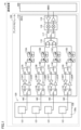
- FIG. 1 is an example of a block diagram of a communication device to which an antenna device is applied.
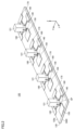
- FIG. 1 is a perspective view (part 1) of an antenna device.
- FIG. 1 is a partially enlarged view (part 1) of the antenna device.
- FIG. 2 is a partially enlarged view (part 2) of the antenna device.
- FIG. 3 is a partially enlarged view (part 3) of the antenna device.
- 6 is a diagram showing a state in which a dielectric block is removed from the antenna device shown in FIG. 5 .
- FIG. 1 is a cross-sectional view (part 1) of an antenna device.
- FIG. 4 is a partially enlarged view of the antenna device.
- FIG. 5 is a partially enlarged view of the antenna device.
- FIG. 6 is a partially enlarged view of the antenna device.
- FIG. 1 is a cross-sectional view (part 1) of an antenna device.
- FIG. 4 is a partially enlarged view of the antenna device.
- FIG. 5 is a partially
- FIG. 7 is a partially enlarged view of the antenna device.
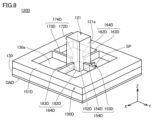
- FIG. 8 is a partially enlarged view of the antenna device.
- FIG. 2 is a cross-sectional view (part 2) of the antenna device.
- FIG. 2 is a second perspective view of the antenna device.
- FIG. 3 is a perspective view of the antenna device.
- FIG. 9 is a partially enlarged view of the antenna device.
- FIG. 10 is a partially enlarged view of the antenna device.
- the (Basic configuration of communication device) 1 is a block diagram of a communication device 10 to which an antenna device 120 according to the present embodiment is applied.
- the communication device 10 is, for example, a mobile terminal such as a mobile phone, a smartphone, or a tablet, or a personal computer equipped with a communication function.
- An example of the frequency band of radio waves used in the antenna device 120 according to the present embodiment is a millimeter wave band radio wave having a center frequency of, for example, 28 GHz, 39 GHz, or 60 GHz, but radio waves of other frequency bands are also applicable.
- the communication device 10 includes an antenna module 100 and a BBIC 200 that constitutes a baseband signal processing circuit.
- the antenna module 100 includes an RFIC 110, which is an example of a power supply device, and an antenna device 120.
- the communication device 10 upconverts an intermediate frequency signal transmitted from the BBIC 200 to the antenna module 100 to a high frequency signal and radiates the high frequency signal from the antenna device 120, and downconverts a high frequency signal received by the antenna device 120 to an intermediate frequency signal and processes the signal in the BBIC 200.
- the antenna device 120 includes a substrate 130 in the shape of a flat plate having a substantially rectangular shape, and a plurality of dielectric blocks 121 arranged on the mounting surface 130a of the substrate 130.
- a substrate 130 in the shape of a flat plate having a substantially rectangular shape, and a plurality of dielectric blocks 121 arranged on the mounting surface 130a of the substrate 130.
- FIG. 1 an example of an array configuration in which four dielectric blocks 121 are arranged in a row on the mounting surface 130a of the substrate 130 is shown, but the number and arrangement of the dielectric blocks 121 are not limited to this.
- a single dielectric block 121 may be arranged on the mounting surface 130a of the substrate 130, or five or more dielectric blocks 121 may be arranged.
- an array configuration in which the dielectric blocks 121 are arranged two-dimensionally may be used.
- the antenna module 100 is a dielectric resonator antenna (DRA).
- the resonance characteristics (corresponding frequency band) of the dielectric block 121 are determined by the shape and dimensions of the dielectric block 121 and the dielectric constant of the dielectric that makes up the block.
- the antenna module 100 In the antenna module 100 according to this embodiment, a high-frequency signal is supplied to each dielectric block 121 from the corresponding power supply wiring 140.
- the antenna module 100 is a so-called single-band, single-polarized type antenna module.
- the RFIC 110 includes switches 111A-111D, 113A-113D, and 117, power amplifiers 112AT-112DT, low-noise amplifiers 112AR-112DR, attenuators 114A-114D, phase shifters 115A-115D, a signal combiner/distributor 116, a mixer 118, and an amplifier circuit 119.
- switches 111A-111D and 113A-113D are switched to the power amplifiers 112AT-112DT side, and switch 117 is connected to the transmitting amplifier of amplifier circuit 119.
- switches 111A-111D and 113A-113D are switched to the low-noise amplifiers 112AR-112DR side, and switch 117 is connected to the receiving amplifier of amplifier circuit 119.
- the received signals which are high-frequency signals received by each dielectric block 121, are transmitted to the RFIC 110 and combined in the signal combiner/distributor 116 via four different signal paths.
- the combined received signals are down-converted to intermediate frequency signals in the mixer 118, and further amplified in the amplifier circuit 119 before being transmitted to the BBIC 200.
- Fig. 2 is a perspective view of the antenna device 120.
- Fig. 3 is a partially enlarged view of the periphery of one dielectric block 121 in the antenna device 120.
- the normal direction of the mounting surface 130a of the substrate 130 is referred to as the Z-axis direction
- the direction along the short side of the mounting surface 130a is referred to as the X-axis direction
- the direction along the long side of the mounting surface 130a is referred to as the Y-axis direction.
- the positive direction of the Z-axis may be referred to as the upper side
- the negative direction as the lower side.
- the dielectric block 121 has a rectangular parallelepiped (more specifically, a square prism) shape. Note that the shape of the dielectric block 121 need only be a columnar shape, and is not necessarily limited to a rectangular parallelepiped shape. For example, the dielectric block 121 may be cylindrical.
- a number of plate-shaped metal frames 150, 160, 170, and 180 are arranged on the mounting surface 130a of the substrate 130.
- One frame 150, 160, 170, and 180 is arranged for each dielectric block 121.
- the substrate 130 may be, for example, a low temperature co-fired ceramics (LTCC) multilayer substrate, a multilayer resin substrate formed by laminating multiple resin layers made of resins such as epoxy and polyimide, a multilayer resin substrate formed by laminating multiple resin layers made of liquid crystal polymer (LCP) having a lower dielectric constant, a multilayer resin substrate formed by laminating multiple resin layers made of fluorine-based resin, a multilayer resin substrate formed by laminating multiple resin layers made of PET (Polyethylene Terephthalate), or a ceramic multilayer substrate other than LTCC.
- LCP liquid crystal polymer
- PET Polyethylene Terephthalate
- the substrate 130 does not necessarily have to have a multilayer structure and may be a single-layer substrate.
- a flat-plate shaped ground electrode GND is disposed on the underside of the substrate 130.
- the ground electrode GND is not necessarily limited to being disposed on the underside of the substrate 130, but may be disposed on a middle layer of the substrate 130 or on the mounting surface 130a (upper surface) of the substrate 130.
- the dielectric block 121 is disposed on the mounting surface 130a of the substrate 130. Therefore, the dielectric block 121 is disposed facing the ground electrode GND.
- the resonant frequency of the dielectric block 121 depends on the length of the side of the top surface of the dielectric block 121, and the frequency bandwidth of the dielectric block 121 depends on the height (dimension in the Z-axis direction) of the dielectric block 121.
- the power supply wiring 140 is disposed in the middle layer of the substrate 130. Note that the power supply wiring 140 is not necessarily limited to being disposed in the middle layer of the substrate 130, and may be disposed, for example, on the mounting surface 130a (upper surface) of the substrate 130.
- One end of the power supply wiring 140 is connected to the RFIC 110 (see FIG. 1).
- the other end of the power supply wiring 140 is connected to a power supply point SP arranged on the mounting surface 130a of the substrate 130 via a via or the like.
- the frame 150 has a main body 151 disposed at a position spaced apart from the dielectric block 121 in the positive direction of the Y axis, and a protrusion 154 protruding in the negative direction of the Y axis from the main body 151 toward the dielectric block 121.
- the main body 151 is connected to the ground electrode GND through a via 141.
- the protrusion 154 includes a terminal portion 152 disposed at the tip of the protrusion 154, a wiring portion 153 disposed between the main body portion 151 and the terminal portion 152, and a branch portion 155 branching off from the wiring portion 153.
- the terminal portion 152 has a surface that abuts against the side surface 121a of the dielectric block 121.
- the surface of the terminal portion 152 that abuts against the side surface 121a (hereinafter also simply referred to as the "abutment surface of the terminal portion 152") extends in the positive direction of the Z axis and faces the side surface 121a of the dielectric block 121.
- the wiring portion 153 extends in the Y-axis direction, with one end connected to the main body portion 151 and the other end connected to the terminal portion 152.
- the dimension of the wiring portion 153 in the Z-axis direction is smaller than the dimension of the terminal portion 152 in the Z-axis direction.
- the terminal portion 152 is bent at approximately 90° with respect to the wiring portion 153.
- the branch portion 155 branches off from the wiring portion 153 and extends in the X-axis direction, with its tip connected to the power supply point SP. This allows the wiring portion 153 to be connected to the power supply wiring 140 at a position closer to the terminal portion 152 than the connection portion with the main body portion 151. Note that the branch portion 155 can be omitted. When the branch portion 155 is omitted, it is sufficient to connect the wiring portion 153 to the power supply point SP at a position closer to the terminal portion 152 than the connection portion with the main body portion 151.
- the frame 160 has a main body 161 disposed at a position away from the dielectric block 121 in the negative direction of the X-axis, and a protruding portion 164 protruding from the main body 161 toward the dielectric block 121 in the positive direction of the X-axis.
- the protruding portion 164 has a terminal portion 162 disposed at the tip of the protruding portion 164 and having a surface that abuts against the side surface 121a of the dielectric block 121, and a wiring portion 163 disposed between the main body 161 and the terminal portion 162.
- the surface of the terminal portion 162 that abuts against the side surface 121a extends in the positive direction of the Z-axis and faces the side surface 121a of the dielectric block 121.
- the dimension of the wiring portion 163 in the Z-axis direction is smaller than the dimension of the terminal portion 162 in the Z-axis direction.
- the terminal portion 162 is bent at approximately 90° with respect to the wiring portion 163.
- the basic configuration of the frame 170 is the same as that of the frame 160.
- the frame 170 has a main body 171 disposed at a position away from the dielectric block 121 in the negative Y-axis direction, and a protruding portion 174 protruding from the main body 171 toward the dielectric block 121 in the positive Y-axis direction.
- the protruding portion 174 includes a terminal portion 172 disposed at the tip of the protruding portion 174 and having a surface that abuts against the side surface 121a of the dielectric block 121, and a wiring portion 173 disposed between the main body 171 and the terminal portion 172.
- the surface of the terminal portion 172 that abuts against the side surface 121a (hereinafter also simply referred to as the "abutting surface of the terminal portion 172") extends in the positive Z-axis direction and faces the side surface 121a of the dielectric block 121.
- the dimension of the wiring portion 173 in the Z-axis direction is smaller than the dimension of the terminal portion 172 in the Z-axis direction.
- the terminal portion 172 is bent at approximately 90° with respect to the wiring portion 173.
- the basic configuration of the frame 180 is the same as that of the frame 160.
- the frame 180 has a main body 181 disposed at a position away from the dielectric block 121 in the positive direction of the X-axis, and a protruding portion 184 protruding from the main body 181 toward the dielectric block 121 in the negative direction of the X-axis.
- the protruding portion 184 includes a terminal portion 182 disposed at the tip of the protruding portion 184 and having a surface that abuts against the side surface 121a of the dielectric block 121, and a wiring portion 183 disposed between the main body 181 and the terminal portion 182.
- the surface of the terminal portion 182 that abuts against the side surface 121a extends in the positive direction of the Z-axis and faces the side surface 121a of the dielectric block 121.
- the dimension of the wiring portion 183 in the Z-axis direction is smaller than the dimension of the terminal portion 182 in the Z-axis direction.
- the terminal portion 182 is bent at approximately 90° with respect to the wiring portion 183.
- the main body parts 151, 161, 171, and 181 are arranged at different positions so as to surround the periphery of the dielectric block 121. Specifically, the main body parts 151, 161, 171, and 181 are each arranged in the normal direction of the four faces that form the side surface 121a of the dielectric block 121.
- the terminal portions 152, 162, 172, and 182 are in contact with the four faces that form the side surface 121a of the dielectric block 121.
- the terminal portions 152 and 172 are located in different regions.
- the terminal portions 162 and 182 are located in different regions.
- the wiring section 153 of the frame 150 extends linearly in the normal direction (Y-axis direction) of the abutment surface of the terminal section 152.
- the wiring section 163 of the frame 160 extends linearly in the normal direction (X-axis direction) of the abutment surface of the terminal section 162.
- the wiring section 173 of the frame 170 extends linearly in the normal direction (Y-axis direction) of the abutment surface of the terminal section 172.
- the wiring section 183 of the frame 180 extends linearly in the normal direction (X-axis direction) of the abutment surface of the terminal section 182.
- the mounting surface 130a of the substrate 130 is provided with the rectangular parallelepiped dielectric block 121 and the flat metal frame 150.
- the frame 150 has a main body 151 located away from the dielectric block 121, a wiring portion 153 extending from the main body 151 toward the dielectric block 121, a terminal portion 152 located at the tip of the wiring portion 153, and a branch portion 155 branching off from the wiring portion 153 and connected to the power supply point SP (power supply wiring 140).
- the terminal portion 152 of the frame 150 has an abutment surface that extends in the Z-axis direction and abuts against the side surface 121a of the dielectric block 121. Therefore, compared to a case where a long and thin conductor is abutted against the side surface 121a of the dielectric block 121, the dielectric block 121 is supported more strongly, making it difficult for the dielectric block 121 to displace toward the frame 150, for example.
- the branch 155 of the frame 150 is connected to the power supply point SP (power supply wiring 140). Therefore, a high-frequency signal from the power supply point SP can be supplied to the side surface 121a of the dielectric block 121 via the branch 155 of the frame 150, a part of the wiring portion 153, and the terminal portion 152.
- frames 160, 170, and 180 are provided on the mounting surface 130a of the substrate 130. These frames 160, 170, and 180 have main body portions 161, 171, and 181, wiring portions 163, 173, and 183, and terminal portions 162, 172, and 182, respectively.
- the terminal portion 152 of the frame 150 and the terminal portions 162, 172, 182 of the frames 160, 170, 180 have abutment surfaces that abut at different positions on the side surface 121a of the dielectric block 121, specifically, the four surfaces that form the side surface 121a.
- These frames 150, 160, 170, 180 can hold the dielectric block 121 so that it does not displace in the direction along the mounting surface 130a.
- the main body portions 151, 161, 171, and 181 are arranged so as to surround the periphery of the dielectric block 121 when viewed in a plan view from the Z-axis direction.
- the wiring portions 153, 163, 173, and 183 extend linearly in the normal direction of the contact surfaces of the terminal portions 152, 162, 172, and 182, respectively. This makes it possible to minimize the length of the wiring portions 153, 163, 173, and 183 and suppress deterioration of the antenna characteristics due to the generation of unnecessary modes.
- the antenna device 120 can suppress such problems.
- the terminal portion 152 and the terminal portion 172 are arranged in different regions so as to sandwich the dielectric block 121.
- the terminal portion 162 and the terminal portion 182 are arranged in different regions so as to sandwich the dielectric block 121. This improves the holding force of the dielectric block 121 by the frames 150, 160, 170, and 180.
- the wiring portion 153 of the frame 150 is connected at one end to the dielectric block 121, and at the other end to the main body portion 151 connected to the ground electrode GND.
- the branch portion 155 of the frame 150 branches from a point closer to the terminal portion 152 than the connection portion of the wiring portion 153 with the main body portion 151.
- the wiring portion 153 of the frame 150 is connected to the power supply point SP (power supply wiring 140) at a point closer to the terminal portion 152 than the connection portion with the main body portion 151.
- the wiring portion 153 itself connected to the power supply point SP can be made to act as a short stub to perform matching adjustment. By performing matching adjustment, the antenna gain can be improved.
- the main body parts 151, 161, 171, and 181 of the frames 150, 160, 170, and 180 are divided into small parts and arranged on the mounting surface 130a. This reduces the area that the main body parts 151, 161, 171, and 181 occupy on the mounting surface 130a, and other components, wiring, matching circuits, etc. can be arranged in the freed up space.
- the terminal portions 152, 162, 172, 182 are bent with respect to the wiring portions 153, 163, 173, 183, respectively, and abut against the side surface 121a of the dielectric block 121. Therefore, the terminal portions 152, 162, 172, 182 that hold the dielectric block 121 are firmly supported by the wiring portions 153, 163, 173, 183 and the main body portions 151, 161, 171, 181. As a result, the holding force of the dielectric block 121 can be further strengthened compared to when the terminal portions 152, 162, 172, 182 are arranged alone without being connected to the wiring portions 153, 163, 173, 183 and the main body portions 151, 161, 171, 181.
- the “communication device 10" and “antenna device 120" may correspond to the “communication device” and “antenna device” of this disclosure.
- the “substrate 130,” “mounting surface 130a,” “ground electrode GND,” and “power supply wiring 140" in this embodiment may correspond to the “substrate,” “mounting surface,” “ground electrode,” and “power supply wiring” of this disclosure, respectively.
- the "dielectric block 121" and “side surface 121a” in this embodiment may correspond to the “dielectric block” and “side surface” of this disclosure, respectively.
- the "frame 150,” "main body 151,” “protrusion 154,” “terminal 152,” “contact surface of terminal 152,” “wiring 153,” and “Z-axis direction” in this embodiment may correspond to the "first frame,” “first main body,” “first protrusion,” “first terminal,” “first contact surface,” “first wiring,” and “first direction” of the present disclosure, respectively.
- the "frames 160, 170, 180,” “main body portions 161, 171, 181,” “protrusions 164, 174, 184,” “terminal portions 162, 172, 182,” and “wiring portions 163, 173, 183" of this embodiment may correspond to the "second frame,” “second main body portion,” “second protrusions,” “second terminal portions,” and “second wiring portions” of the present disclosure, respectively.
- the main bodies 151, 161, 171, and 181 are separate, but the main bodies 151, 161, 171, and 181 may be integrally formed.
- FIG. 4 is a partially enlarged view of the periphery of one dielectric block 121 in the antenna device 120A according to this modification example 1.
- the four frames 150, 160, 170, and 180 of the antenna device 120 according to the above embodiment are replaced with a single frame 150A.
- the main body portions 151, 161, 171, and 181 of the antenna device 120 according to the above embodiment are replaced with an integrally formed main body portion 151A.
- the main body portion 151A is disposed so as to surround the entire periphery of the dielectric block 121.
- the protrusions 154, 164, 174, and 184 of the frame 150A protrude from the integrally formed main body portion 151A toward the dielectric block 121.
- the "main body portion 151A" according to this modification 1 may correspond to the "first main body portion” and the “second main body portion” of the present disclosure formed integrally.
- the dielectric block 121 is placed on the mounting surface 130 a of the substrate 130 , but the dielectric block 121 may be fitted into a recess in the substrate 130 .
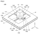
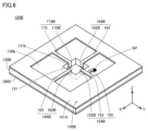
- FIG. 5 is a partially enlarged view of the periphery of one dielectric block 121 in the antenna device 120B according to the present modified example 2.
- FIG. 6 is a view showing the antenna device 120B shown in FIG. 5 with the dielectric block 121 removed.
- the board 130 and the frame 150A of the antenna device 120A according to the above modified example 1 are replaced with board 130B and frame 150B, respectively.
- the protrusions 154, 164, 174, and 184 of the frame 150A according to the above modified example 1 are replaced with protrusions 154B, 164B, 174B, and 184B, respectively.
- a recess 131 recessed in the negative direction of the Z axis is formed near the center of the mounting surface 130b of the substrate 130B.
- the ground electrode GND has a portion disposed in a position overlapping the recess 131.
- the recess 131 may be a hole penetrating the substrate 130B including the ground electrode GND.
- the lower part of the dielectric block 121 is fitted into a recess 131 of the substrate 130B.
- the protrusion 154B has a wiring portion 153 and a terminal portion 152B.
- the terminal portion 152B is bent at approximately 90° with respect to the wiring portion 153 so as to fit along the inner wall 131b of the recess 131.
- the terminal portion 162B of the protrusion 164B, the terminal portion 172B of the protrusion 174B, and the terminal portion 182B of the protrusion 184B are also bent at approximately 90° with respect to the wiring portions 163, 173, and 183, respectively, so as to fit along the inner wall of the recess 131.
- the terminal portions 152B, 162B, 172B, and 182B are disposed between the inner wall of the recess 131 and the side surface 121a of the dielectric block 121.
- the dielectric block 121 is fitted into the recess 131 of the substrate 130, so that the height of the dielectric block 121 from the mounting surface 130b can be kept low, and the dielectric block 121 can be held by the inner wall of the recess 131, improving the holding force of the dielectric block 121.
- the ground electrode GND is arranged at a position overlapping the recess 131 when the substrate 130B is viewed in a plan view from the Z-axis direction. Therefore, the lower surface of the dielectric block 121 can be made to face the ground electrode GND. This can improve the antenna characteristics as a dielectric resonator antenna.
- the "recess 131" and the “inner wall 131b of recess 131" according to this modification 2 may correspond to the "recess” and the “inner wall of the recess” of the present disclosure, respectively.
- At least one of the terminal portions 152B, 162B, 172B, 182B of the second modified example described above may be modified to have a shape that is elastically deformable in the normal direction of the side surface 121a of the dielectric block 121 with which it comes into contact.
- FIG. 7 is a cross-sectional view of the antenna device 120C according to the third modification taken along the YZ plane.
- the terminal portions 152C, 172C according to the third modification extend in the Z-axis direction while being bent in a zigzag shape.
- terminal portion 152C and terminal portion 172C" according to this modification example 3 may correspond to the "first terminal portion” and “second terminal portion” of the present disclosure, respectively.
- each of the terminal portions 152, 162, 172, 182 is bent relative to the wiring portions 153, 163, 173, 183 and abuts against the side surface 121a of the dielectric block 121.
- the thickness (dimension in the Z-axis direction) of each wiring portion may be increased to the height (dimension in the Z-axis direction) of each terminal portion and the tip surface of each terminal portion may be abutted against the side surface 121a of the dielectric block 121.
- FIG. 8 is a partially enlarged view of the periphery of one dielectric block 121 in the antenna device 120D according to the fourth modification.
- the antenna device 120D is obtained by replacing the frame 150A of the antenna device 120A according to the first modification described above with a frame 150D.
- Frame 150D is a frame in which the thickness (dimension in the Z-axis direction) of main body 151A and wiring portions 153, 163, 173, and 183 of frame 150A according to the above-mentioned modification example 1 is increased to the height (dimension in the Z-axis direction) of terminal portions 152, 162, 172, and 182 of frame 150A.
- the frame 150D has a main body 151D and protruding parts 154D, 164D, 174D, and 184D.
- the heights (dimensions in the Z-axis direction) of the main body 151D and the protruding parts 154D, 164D, 174D, and 184D are approximately equal.
- Protrusion 154D has terminal portion 152D, wiring portion 153D, and branch portion 155D.
- the height (dimension in the Z-axis direction) of wiring portion 153D is greater than the width (dimension in the X-axis direction) of wiring portion 153D and is approximately equal to the height (dimension in the Z-axis direction) of terminal portion 152D.
- terminal portion 152D is the tip surface of wiring portion 153D.
- Protrusion 164D has terminal portion 162D and wiring portion 163D.
- the height (dimension in the Z-axis direction) of wiring portion 163D is greater than the width (dimension in the Y-axis direction) of wiring portion 163D and is approximately equal to the height (dimension in the Z-axis direction) of terminal portion 162D.
- terminal portion 162D is the tip surface of wiring portion 163D.
- protrusion 174D has terminal portion 172D and wiring portion 173D.
- the height (dimension in the Z-axis direction) of wiring portion 173D is greater than the width (dimension in the X-axis direction) of wiring portion 173D and is approximately equal to the height (dimension in the Z-axis direction) of terminal portion 172D.
- terminal portion 172D is the tip surface of wiring portion 173D.
- protrusion 184D has terminal portion 182D and wiring portion 183D.
- the height (dimension in the Z-axis direction) of wiring portion 183D is greater than the width (dimension in the Y-axis direction) of wiring portion 183D and is approximately equal to the height (dimension in the Z-axis direction) of terminal portion 182D.
- terminal portion 182D is the tip surface of wiring portion 183D.
- each wiring portion 153D, 163D, 173D, and 183D may be increased so that the tip surface of each wiring portion 153D, 163D, 173D, and 183D abuts against the side surface 121a of the dielectric block 121.
- the stability of the posture of the dielectric block 121 is increased, and as a result, the antenna characteristics as a dielectric resonator antenna can be stabilized.
- the "tip surface of wiring portion 153D" and the “tip surfaces of wiring portions 163D, 173D, and 183D” according to this modification 4 may correspond to the "tip surface of the first wiring portion” and the "tip surface of the second wiring portion” of the present disclosure, respectively.
- the dielectric block 121 is held by four protrusions, but the number of protrusions that hold the dielectric block 121 may be five or more.
- FIG. 9 is a partially enlarged view of the periphery of one dielectric block 121 in the antenna device 120E according to the present modified example 5.
- the antenna device 120E is obtained by replacing the frame 150D of the antenna device 120D according to the above modified example 4 with the frame 150E.
- the dielectric block 121 is held by a total of six protrusions 154D, 164D, 174D, 184D, 210, and 220. This increases the stability of the position of the dielectric block 121, and stabilizes the antenna characteristics as a dielectric resonator antenna.
- the height of the wiring portion of the power supply protrusion connected to the power supply point SP is approximately equal to the height of the wiring portion of the other holding protrusions, but the height of the wiring portion of the power supply protrusion and the height of the wiring portion of the holding protrusion may be made different.
- FIG. 10 is a partially enlarged view of the periphery of one dielectric block 121 in an antenna device 120F according to an example of the sixth modified example.
- the frame 160F of the antenna device 120F has a power supply protrusion 154 and holding protrusions 164D, 174D, 184D, 210, 220, 230, and 240.
- the power supply protrusion 154 has a thin plate shape, similar to the frame 150 in the above-mentioned embodiment, and its tip is bent at approximately 90 degrees relative to the wiring portion and abuts against the side surface 121a of the dielectric block 121.
- the holding protrusions 164D, 174D, 184D, 210, 220, 230, and 240 are higher than the height of the wiring portion of the power supply protrusion 154, and their tip surfaces abut against the side surface 121a of the dielectric block 121.
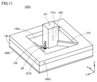
- FIG. 11 is a partially enlarged view of the periphery of one dielectric block 121 in an antenna device 120G according to another example of the sixth modified example.
- Frame 160G of antenna device 120G is obtained by removing holding protrusions 164D, 174D, 184D, 230, 240 from frame 160F of antenna device 120F in FIG. 10 described above. That is, frame 160G has power supply protrusion 154 having a thin plate shape, and holding protrusions 210, 220 that are thicker than power supply protrusion 154.
- FIG. 12 is a partially enlarged view of the periphery of one dielectric block 121 in an antenna device 120H according to the seventh modified example.
- the antenna device 120H is obtained by adding a first electrode pattern 156 and second electrode patterns 166, 176, and 186 to the antenna device 120 according to the above-described embodiment.
- the first electrode pattern 156 is disposed between the power supply protrusion 154 and the mounting surface 130a of the board in contact with the protrusion 154, and is connected to the power supply point SP. When viewed in a plan view from the Z-axis direction, the first electrode pattern 156 is disposed along the power supply protrusion 154 at a position that overlaps with the power supply protrusion 154.
- the first electrode pattern 156 By arranging the first electrode pattern 156 in this manner, even if the distance between the power supply protrusion 154 and the ground electrode GND arranged on the lower layer of the substrate 130 varies due to manufacturing variability, there is no electrical effect. As a result, the electrical characteristics of the power supply protrusion 154 can be stabilized.
- the second electrode patterns 166, 176, 186 are disposed between the holding protrusions 164, 174, 184 and the mounting surface 130a of the board in contact with the protrusions 164, 174, 184.
- the second electrode patterns 166, 176, 186 are disposed at positions that overlap the holding protrusions 164, 174, 184, respectively, when viewed in a plan view from the Z-axis direction.
- FIG. 13 is a cross-sectional view of antenna device 120H cut in the YZ plane passing through second electrode pattern 176.
- second electrode pattern 176 is connected to a ground electrode GND arranged on the lower layer of substrate 130 through via 177.
- other second electrode patterns 166, 186 are also connected to ground electrodes GND arranged on the lower layer of substrate 130 through vias, similar to second electrode pattern 176.
- the "first electrode pattern 156" and the “second electrode patterns 166, 176, 186" according to this modification 7 may correspond to the "first electrode pattern” and “second electrode pattern” of the present disclosure, respectively.
- the main body portions 151, 161, 171, and 181 of the frame are arranged so as to surround the periphery of the dielectric block 121, but the main body portion of the frame is not necessarily limited to being arranged so as to surround the periphery of the dielectric block 121.
- FIG. 14 is a perspective view of an antenna device 120I according to an example of the eighth modified example.
- one frame body is arranged on each side of one dielectric block in the X-axis direction, sandwiching the dielectric block.
- FIG. 15 is a perspective view of an antenna device 120J according to another example of the eighth modified example.
- one frame body is arranged on each side of one dielectric block 121 in the Y-axis direction.
- one dielectric block has one protruding portion for power supply, but the number of protruding portions for power supply for one dielectric block may be two or more.
- FIG. 16 is a partially enlarged view of the periphery of one dielectric block 121 in an antenna device 120K according to an example of the ninth modified example.
- the frame 160 of the antenna device 120 according to the above-described embodiment is replaced with a frame 160K.
- frame 160K has a protrusion for power supply rather than a holding protrusion. That is, frame 160K has a main body portion that is positioned away from dielectric block 121 in the negative direction of the X-axis, and a protrusion that protrudes from the main body portion toward dielectric block 121 in the positive direction of the X-axis.
- the protrusion of frame 160K has the same configuration as the protrusion of frame 150, and is connected to power supply point SP2.
- antenna device 120K a high-frequency signal can be supplied to each dielectric block 121 from the protruding portion of frame 150 and a high-frequency signal can be supplied from the protruding portion of frame 160K.
- the polarization direction of the radiated radio waves differs depending on the position at which the high-frequency signal is fed to dielectric block 121.
- antenna device 120K is a so-called dual-polarized type antenna module that can radiate radio waves in two different polarization directions.
- frame 170L has a protrusion for power supply rather than a holding protrusion. That is, frame 170L has a main body portion that is positioned away from dielectric block 121 in the negative Y-axis direction, and a protrusion portion that protrudes from the main body portion toward dielectric block 121 in the positive Y-axis direction.
- the protrusion portion of frame 170L has the same configuration as the protrusion portion of frame 150, and is connected to power supply point SP3.
- a high-frequency signal from the protruding portion of the frame 150 and a high-frequency signal from the protruding portion of the frame 170L can be supplied to each dielectric block 121.
- the characteristics of the radio waves radiated from each dielectric block 121 can be adjusted.
- the antenna device includes a substrate on which a ground electrode and a power supply wiring are formed, a dielectric block disposed on a mounting surface of the substrate and having a side intersecting the mounting surface, and a plate-shaped metal first frame disposed on the mounting surface.
- the first frame has a first body portion disposed at a position away from the dielectric block, and a first protrusion protruding from the first body portion toward the dielectric block.
- the first protrusion includes a first terminal portion disposed at the tip of the first protrusion and having a first abutment surface that abuts against the side of the dielectric block, and a first wiring portion disposed between the first body portion and the first terminal portion.
- the first abutment surface extends in the first direction and faces the side of the dielectric block.
- the first wiring portion is connected to the power supply wiring.
- the antenna device described in 1 further includes a plurality of second frames made of plate-like metal, each of which is arranged on the mounting surface.
- Each of the plurality of second frames has a second main body portion arranged at a position away from the dielectric block, and a second protrusion portion protruding from the second main body portion toward the dielectric block.
- the second protrusion portion includes a second terminal portion arranged at the tip of the second protrusion portion and having a second abutment surface that abuts against a side surface of the dielectric block, and a second wiring portion arranged between the second main body portion and the second terminal portion.
- the second abutment surface extends in the first direction and faces the side surface of the dielectric block.
- the first body portion and the second body portion are arranged at different positions so as to surround the periphery of the dielectric block when viewed in a plan view from the first direction.
- the first wiring portion extends linearly in the normal direction of the first abutment surface.
- Each of the second wiring portions extends linearly in the normal direction of the corresponding second abutment surface.
- the first wiring portion is connected to the power supply wiring at a point closer to the first terminal portion than the connection portion with the first body portion.
- the first body portion is connected to the ground electrode.
- the dimension of the first wiring portion in the first direction is smaller than the dimension of the first terminal portion in the first direction.
- the first terminal portion is bent relative to the first wiring portion.
- the dimension of the second wiring portion in the first direction is smaller than the dimension of the corresponding second terminal portion in the first direction.
- the second terminal portion is bent relative to the corresponding second wiring portion.
- the dimension of the first wiring portion in the first direction is smaller than the dimension of the first terminal portion in the first direction.
- the first terminal portion is bent with respect to the first wiring portion.
- the dimension of the second wiring portion in the first direction is larger than the dimension of the second wiring portion in a direction perpendicular to the first direction, and is approximately equal to the dimension of the corresponding second terminal portion in the first direction.
- the second abutment surface is the tip surface of the corresponding second wiring portion.
- the dimension of the first wiring portion in the first direction is greater than the dimension of the first wiring portion in the direction perpendicular to the first direction, and is approximately equal to the dimension of the first terminal portion in the first direction.
- the first abutment surface is the tip surface of the first wiring portion.
- the dimension of the second wiring portion in the first direction is greater than the dimension of the second wiring portion in the direction perpendicular to the first direction, and is approximately equal to the dimension of the corresponding second terminal portion in the first direction.
- the second abutment surface is the tip surface of the corresponding second wiring portion.
- the first body portion and the second body portion are integrally formed.
- a recess recessed in the first direction is formed on the mounting surface.
- a part of the dielectric block is disposed in the recess.
- the first terminal portion and the second terminal portion are disposed between the inner wall of the recess and the side surface of the dielectric block.
- the first terminal portion is configured to be elastically deformable in the normal direction of the first contact surface.
- Each of the second terminal portions is configured to be elastically deformable in the normal direction of the side surface of the dielectric block with which it contacts.
- the total number of first protrusions and second protrusions is 4 or more.
- a first electrode pattern is formed on the mounting surface.
- the substrate is viewed in a plan view from the first direction, at least a portion of the first electrode pattern is disposed in a position that overlaps with the first wiring portion.
- a second electrode pattern connected to the ground electrode is formed on the mounting surface.
- the substrate is viewed in a plan view from the first direction, at least a portion of the second electrode pattern is disposed in a position overlapping the second wiring portion.
- a communication device is equipped with an antenna device described in any one of the 1 to 18 paragraphs.
Landscapes
- Details Of Aerials (AREA)
Abstract
アンテナ装置(120)は、基板(130)と、誘電体ブロック(121)と、板状の金属製のフレーム(150)とを備える。フレーム(150)は、本体部(151)と、本体部(151)から突出する突出部(154)とを有する。突出部(154)は、突出部(154)の先端に配置され、誘電体ブロックの側面(121a)に当接する当接面を有する端子部(152)と、本体部(151)と端子部(152)との間に配置される配線部(153)とを含む。端子部(152)の当接面は、基板(130)の実装面(130a)の法線方向に延在して誘電体ブロックの側面(121a)と対向している。配線部(153)は、分岐部(155)を介して給電配線(140)に接続されている。
Description
本開示は、アンテナ装置およびそれを搭載する通信装置に関する。
特開2004-201018号公報(特許文献1)には、平板形状の基板上に配置された誘電体材料の柱体(誘電体ブロック)に高周波信号を供給して電波を放射させる、誘電体共振器アンテナ(DRA:Dielectric Resonator Antenna)が開示されている。この誘電体共振器アンテナにおいては、基板の実装面から基板の実装面の法線方向に沿って直線状に延びる細長い給電線が誘電体ブロックの側面に接しており、この給電線から誘電体ブロックに給電される。
特開2004-201018号公報に開示された誘電体共振器アンテナは誘電体ブロックの側面に給電線が接する構造を有するが、この構造では誘電体ブロックを基板の実装面に沿う方向に対して支持することが容易ではないという問題がある。具体的には、誘電体ブロックの側面に接する給電線は、直線状に延びる細長い導線に過ぎないため、誘電体ブロックを基板の実装面に沿う方向に対して十分に支持することができないことが懸念される。
本開示は、上記のような課題を解決するためになされたものであり、その目的は、誘電体共振器アンテナにおいて、誘電体ブロックの支持と誘電体ブロックへの給電とを実現することである。
本開示によるアンテナ装置は、接地電極および給電配線が形成された基板と、基板の実装面に配置され実装面と交差する側面を有する誘電体ブロックと、実装面に配置された板状の金属製の第1フレームとを備える。第1フレームは、誘電体ブロックとは離れた位置に配置される第1本体部と、第1本体部から誘電体ブロックに向けて突出する第1突出部とを有する。第1突出部は、第1突出部の先端に配置され、誘電体ブロックの側面に当接する第1当接面を有する第1端子部と、第1本体部と第1端子部との間に配置される第1配線部とを含む。実装面の法線方向を第1方向とするとき、第1当接面は、第1方向に延在して誘電体ブロックの側面と対向している。第1配線部は、給電配線に接続されている。
本開示によれば、誘電体共振器アンテナにおいて、誘電体ブロックの支持と誘電体ブロックへの給電とを実現することができる。
以下、本開示の実施の形態について、図面を参照しながら詳細に説明する。なお、図中同一または相当部分には同一符号を付してその説明は繰り返さない。
(通信装置の基本構成)
図1は、本実施の形態に係るアンテナ装置120が適用される通信装置10のブロック図である。通信装置10は、たとえば、携帯電話、スマートフォンあるいはタブレットなどの携帯端末や、通信機能を備えたパーソナルコンピュータなどである。本実施の形態に係るアンテナ装置120に用いられる電波の周波数帯域の一例は、たとえば28GHz、39GHzおよび60GHzなどを中心周波数とするミリ波帯の電波であるが、上記以外の周波数帯域の電波についても適用可能である。
図1は、本実施の形態に係るアンテナ装置120が適用される通信装置10のブロック図である。通信装置10は、たとえば、携帯電話、スマートフォンあるいはタブレットなどの携帯端末や、通信機能を備えたパーソナルコンピュータなどである。本実施の形態に係るアンテナ装置120に用いられる電波の周波数帯域の一例は、たとえば28GHz、39GHzおよび60GHzなどを中心周波数とするミリ波帯の電波であるが、上記以外の周波数帯域の電波についても適用可能である。
図1を参照して、通信装置10は、アンテナモジュール100と、ベースバンド信号処理回路を構成するBBIC200とを備える。アンテナモジュール100は、給電装置の一例であるRFIC110と、アンテナ装置120とを備える。通信装置10は、BBIC200からアンテナモジュール100へ伝達された中間周波数信号を高周波信号にアップコンバートしてアンテナ装置120から放射するとともに、アンテナ装置120で受信した高周波信号を中間周波数信号にダウンコンバートしてBBIC200にて信号を処理する。
アンテナ装置120は、略矩形形状を有する平板形状の基板130と、基板130の実装面130aに配置された複数の誘電体ブロック121を含む。図1においては、基板130の実装面130aに、4つの誘電体ブロック121が一列に配置されたアレイ構成の例が示されているが、誘電体ブロック121の数および配置はこれに限らない。基板130の実装面130aに単独の誘電体ブロック121が配置されていてもよいし、5つ以上の誘電体ブロック121が配置されていてもよい。また、誘電体ブロック121が二次元的に配列されたアレイ構成であってもよい。
誘電体ブロック121に所定の周波数帯域の高周波信号が供給されると、誘電体ブロック121の内部で電界が共振し、当該共振周波数に対応した電波が誘電体ブロック121から外部に放射される。すなわち、アンテナモジュール100は、誘電体共振器アンテナ(DRA)である。誘電体ブロック121の共振特性(対応する周波数帯域)は、誘電体ブロック121の形状、寸法およびブロックを構成する誘電体の誘電率によって決まる。
本実施の形態によるアンテナモジュール100においては、各誘電体ブロック121に対して、対応する給電配線140からの高周波信号が供給される。アンテナモジュール100は、いわゆるシングルバンド・シングル偏波タイプのアンテナモジュールである。
RFIC110は、スイッチ111A~111D,113A~113D,117と、パワーアンプ112AT~112DTと、ローノイズアンプ112AR~112DRと、減衰器114A~114Dと、移相器115A~115Dと、信号合成/分配器116と、ミキサ118と、増幅回路119とを備える。
高周波信号を送信する場合には、スイッチ111A~111D,113A~113Dがパワーアンプ112AT~112DT側へ切換えられるとともに、スイッチ117が増幅回路119の送信側アンプに接続される。高周波信号を受信する場合には、スイッチ111A~111D,113A~113Dがローノイズアンプ112AR~112DR側へ切換えられるとともに、スイッチ117が増幅回路119の受信側アンプに接続される。
BBIC200から伝達された中間周波数信号は、増幅回路119で増幅され、ミキサ118でアップコンバートされる。アップコンバートされた高周波信号である送信信号は、信号合成/分配器116で4分波され、対応する信号経路を通過して、それぞれ異なる誘電体ブロック121に給電される。各信号経路に配置された移相器115A~115Dの移相度が個別に調整されることにより、誘電体ブロック121から出力される電波の指向性を調整することができる。また、減衰器114A~114Dは送信信号の強度を調整する。
各誘電体ブロック121で受信された高周波信号である受信信号はRFIC110に伝達され、異なる4つの信号経路を経由して信号合成/分配器116において合波される。合波された受信信号はミキサ118で中間周波数信号へダウンコンバートされ、さらに増幅回路119で増幅されてBBIC200へ伝達される。
RFIC110は、例えば、1チップの集積回路部品として形成される。あるいは、各誘電体ブロックに対応する機器(スイッチ、パワーアンプ、ローノイズアンプ、減衰器、移相器)について、対応する誘電体ブロック毎に1チップの集積回路部品として形成されてもよい。
(アンテナモジュールの構造)
次に、図2および図3を用いて、アンテナ装置120の構成の詳細を説明する。図2は、アンテナ装置120の斜視図である。図3は、アンテナ装置120における1つの誘電体ブロック121の周辺を部分的に拡大した図である。
次に、図2および図3を用いて、アンテナ装置120の構成の詳細を説明する。図2は、アンテナ装置120の斜視図である。図3は、アンテナ装置120における1つの誘電体ブロック121の周辺を部分的に拡大した図である。
なお、以降の説明において、基板130の実装面130aの法線方向をZ軸方向とし、実装面130aの短辺に沿った方向をX軸方向とし、実装面130aの長辺に沿った方向をY軸方向とする。各図においてZ軸の正方向を上方側、負方向を下方側と称する場合がある。
誘電体ブロック121は、直方体(より詳しくは正四角柱)形状を有している。なお、誘電体ブロック121の形状は、柱形状であればよく、必ずしも直方体形状であることに限定されない。たとえば、誘電体ブロック121は円柱形状であってもよい。
図2に示すように、基板130の実装面130aには、4つの誘電体ブロック121に加えて、複数の板状の金属製のフレーム150,160,170,180がさらに配置される。各誘電体ブロック121につき、フレーム150,160,170,180が1枚ずつ配置されている。
基板130は、たとえば、低温同時焼成セラミックス(LTCC:Low Temperature Co-fired Ceramics)多層基板、エポキシ、ポリイミドなどの樹脂から構成される樹脂層を複数積層して形成された多層樹脂基板、より低い誘電率を有する液晶ポリマー(Liquid Crystal Polymer:LCP)から構成される樹脂層を複数積層して形成された多層樹脂基板、フッ素系樹脂から構成される樹脂層を複数積層して形成された多層樹脂基板、PET(Polyethylene Terephthalate)材から構成される樹脂層を複数積層して形成された多層樹脂基板、あるいは、LTCC以外のセラミックス多層基板である。なお、基板130は必ずしも多層構造でなくてもよく、単層の基板であってもよい。
基板130の下面には、平板形状の接地電極GNDが配置されている。なお、接地電極GNDは、必ずしも基板130の下面に配置されていることに限定されず、基板130の中層に配置されてもよいし、基板130の実装面130a(上面)に配置されていてもよい。
誘電体ブロック121は、基板130の実装面130aに配置されている。したがって、誘電体ブロック121は、接地電極GNDに対向して配置される。このような配置において、誘電体ブロック121に高周波信号が入力される(給電される)と、誘電体ブロック121から接地電極GNDとは反対の方向に電波が放射される。なお、誘電体ブロック121の共振周波数は誘電体ブロック121の天面の辺の長さに依存し、誘電体ブロック121の周波数帯域幅は誘電体ブロック121の高さ(Z軸方向の寸法)に依存する。
給電配線140は、基板130の中層に配置されている。なお、給電配線140は、必ずしも基板130の中層に配置されていることに限定されず、たとえば基板130の実装面130a(上面)に配置されていてもよい。
給電配線140の一方の端部は、RFIC110(図1参照)に接続される。給電配線140の他方の端部は、ビア等を介して基板130の実装面130aに配置された給電点SPに接続されている。
図3を参照して、フレーム150,160,170,180の構成を説明する。
フレーム150は、誘電体ブロック121からY軸正方向に離れた位置に配置される本体部151と、本体部151から誘電体ブロック121に向けてY軸負方向に突出する突出部154とを有する。本体部151は、ビア141を介して接地電極GNDに接続されている。
フレーム150は、誘電体ブロック121からY軸正方向に離れた位置に配置される本体部151と、本体部151から誘電体ブロック121に向けてY軸負方向に突出する突出部154とを有する。本体部151は、ビア141を介して接地電極GNDに接続されている。
突出部154は、突出部154の先端に配置される端子部152と、本体部151と端子部152との間に配置される配線部153と、配線部153から分岐する分岐部155とを含む。
端子部152は、誘電体ブロック121の側面121aに当接する面を有している。端子部152における、側面121aに当接する面(以下、単に「端子部152の当接面」ともいう)は、Z軸正方向に延在して誘電体ブロック121の側面121aと対向している。
配線部153は、Y軸方向に延在し、一方の端部が本体部151に接続され、他方の端部が端子部152に接続される。配線部153のZ軸方向の寸法は、端子部152のZ軸方向の寸法よりも小さい。端子部152は、配線部153に対して略90°屈曲している。
分岐部155は、配線部153から分岐してX軸方向に延在し、先端が給電点SPに接続される。これにより、配線部153は、本体部151との接続部分よりも端子部152に近い位置で給電配線140に接続される。なお、分岐部155は省略可能である。分岐部155を省略する場合、配線部153における本体部151との接続部分よりも端子部152に近い位置で給電点SPに接続すればよい。
フレーム160は、誘電体ブロック121からX軸負方向に離れた位置に配置される本体部161と、本体部161から誘電体ブロック121に向けてX軸正方向に突出する突出部164とを有する。突出部164は、突出部164の先端に配置されて誘電体ブロック121の側面121aに当接する面を有する端子部162と、本体部161と端子部162との間に配置される配線部163とを有する。端子部162における、側面121aに当接する面(以下、単に「端子部162の当接面」ともいう)は、Z軸正方向に延在して誘電体ブロック121の側面121aと対向している。配線部163のZ軸方向の寸法は、端子部162のZ軸方向の寸法よりも小さい。端子部162は、配線部163に対して略90°屈曲している。
フレーム170の基本構成は、フレーム160と同じである。具体的には、フレーム170は、誘電体ブロック121からY軸負方向に離れた位置に配置される本体部171と、本体部171から誘電体ブロック121に向けてY軸正方向に突出する突出部174とを有する。突出部174は、突出部174の先端に配置されて誘電体ブロック121の側面121aに当接する面を有する端子部172と、本体部171と端子部172との間に配置される配線部173とを含む。端子部172における、側面121aに当接する面(以下、単に「端子部172の当接面」ともいう)は、Z軸正方向に延在して誘電体ブロック121の側面121aと対向している。配線部173のZ軸方向の寸法は、端子部172のZ軸方向の寸法よりも小さい。端子部172は、配線部173に対して略90°屈曲している。
フレーム180の基本構成も、フレーム160と同じある。具体的には、フレーム180は、誘電体ブロック121からX軸正方向に離れた位置に配置される本体部181と、本体部181から誘電体ブロック121に向けてX軸負方向に突出する突出部184とを有する。突出部184は、突出部184の先端に配置されて誘電体ブロック121の側面121aに当接する面を有する端子部182と、本体部181と端子部182との間に配置される配線部183とを含む。端子部182における、側面121aに当接する面(以下、単に「端子部182の当接面」ともいう)は、Z軸正方向に延在して誘電体ブロック121の側面121aと対向している。配線部183のZ軸方向の寸法は、端子部182のZ軸方向の寸法よりも小さい。端子部182は、配線部183に対して略90°屈曲している。
本体部151,161,171,181は、Z軸方向から平面視した場合、誘電体ブロック121の周囲を囲むように互いに異なる位置に配置されている。具体的には、本体部151,161,171,181は、誘電体ブロック121の側面121aを形成する4面の法線方向にそれぞれ配置されている。
端子部152,162,172,182は、誘電体ブロック121の側面121aを形成する4面にそれぞれ当接している。言い換えれば、Z軸方向から平面視したときの誘電体ブロック121の領域を誘電体ブロック121の天面中心を通るXZ平面相当の分割線で2つに分割したとき、端子部152と端子部172とは互いに異なる領域に配置される。同様に、Z軸方向から平面視したときの誘電体ブロック121の領域を誘電体ブロック121の天面中心を通るYZ平面相当の分割線で2つに分割したとき、端子部162と端子部182とは互いに異なる領域に配置される。
フレーム150の配線部153は、端子部152の当接面の法線方向(Y軸方向)に直線状に延在している。フレーム160の配線部163は、端子部162の当接面の法線方向(X軸方向)に直線状に延在している。フレーム170の配線部173は、端子部172の当接面の法線方向(Y軸方向)に直線状に延在している。フレーム180の配線部183は、端子部182の当接面の法線方向(X軸方向)に直線状に延在している。
以上のように、本実施の形態によるアンテナ装置120においては、基板130の実装面130aに、直方体形状の誘電体ブロック121と、平板形状の金属製のフレーム150とが備えられる。フレーム150は、誘電体ブロック121とは離れた位置に配置される本体部151と、本体部151から誘電体ブロック121に向けて延在する配線部153と、配線部153の先端部に配置される端子部152と、配線部153から分岐して給電点SP(給電配線140)に接続される分岐部155とを有する。
フレーム150の端子部152は、Z軸方向に延在して誘電体ブロック121の側面121aに対向して当接する当接面を有する。そのため、たとえば細長い導線を誘電体ブロック121の側面121aに当接させる場合に比べて、誘電体ブロック121をより強く支持して誘電体ブロック121がフレーム150側に変位し難くすることができる。
フレーム150の分岐部155は、給電点SP(給電配線140)に接続されている。そのため、給電点SPからの高周波信号を、フレーム150の分岐部155、配線部153の一部、および端子部152を介して、誘電体ブロック121の側面121aに供給することができる。
このような構成を有するフレーム150を設けることによって、誘電体ブロック121への給電と誘電体ブロック121の支持とを実現することができる。
さらに、基板130の実装面130aには、フレーム160,170,180が備えられる。これらのフレーム160,170,180は、それぞれ本体部161,171,181、配線部163,173,183、および端子部162,172,182を有している。
フレーム150の端子部152、およびフレーム160,170,180の端子部162,172,182は、誘電体ブロック121の側面121aの互いに異なる位置、具体的には側面121aを形成する4面に、それぞれ当接する当接面を有している。これらのフレーム150,160,170,180によって、誘電体ブロック121が実装面130aに沿う方向に変位しないように誘電体ブロック121を保持することができる。
さらに、本体部151,161,171,181は、Z軸方向から平面視した場合、誘電体ブロック121の周囲を囲むように配置されている。そして、配線部153,163,173,183は、それぞれ端子部152,162,172,182の当接面の法線方向に直線状に延在している。これにより、配線部153,163,173,183の長さを極力短くして、不要なモードの発生によるアンテナ特性の劣化を抑制することができる。すなわち、配線部153,163,173,183が長くなると、その分、不要なモードが発生して誘電体共振器アンテナとしてのアンテナ特性が劣化してしまうことが問題となり得るが、本実施の形態によるアンテナ装置120においては、そのような問題を抑制し得る。
さらに、誘電体ブロック121を誘電体ブロック121の天面中心を通るXZ平面で2つに分割したとき、端子部152と端子部172とは、誘電体ブロック121を挟み込むように互いに異なる領域に配置される。同様に、誘電体ブロック121を誘電体ブロック121の天面中心を通るYZ平面で2つに分割したとき、端子部162と端子部182とは、誘電体ブロック121を挟み込むように互いに異なる領域に配置される。これにより、フレーム150,160,170,180による誘電体ブロック121の保持力を向上することができる。
さらに、フレーム150の配線部153は、一方の端部で誘電体ブロック121と接続され、他方の端部で接地電極GNDに接続された本体部151と接続される。そして、フレーム150の分岐部155は、配線部153における本体部151との接続部分よりも端子部152に近い点から分岐している。言い換えれば、フレーム150の配線部153は、本体部151との接続部分よりも端子部152に近い点で給電点SP(給電配線140)に接続される。このような構成によって、給電点SP(給電配線140)に接続される配線部153自体をショートスタブとして作用させて、マッチング調整を行なうことができる。マッチング調整を行なうことによってアンテナゲインを向上させることができる。
さらに、本実施の形態によるアンテナ装置120においては、フレーム150,160,170,180の本体部151,161,171,181が、小さく分割されて実装面130aに配置されている。これにより、実装面130a上における本体部151,161,171,181の占有面積を小さくし、空いたスペースに他の部品、配線、整合回路等を配置することができる。
さらに、本実施の形態によるアンテナ装置120においては、端子部152,162,172,182が、配線部153,163,173,183に対してそれぞれ屈曲して誘電体ブロック121の側面121aに当接している。したがって、誘電体ブロック121を保持する端子部152,162,172,182が、配線部153,163,173,183および本体部151,161,171,181によってしっかりと支持される。その結果、端子部152,162,172,182が配線部153,163,173,183および本体部151,161,171,181に接続されずに単独で配置される場合に比べて、誘電体ブロック121の保持力をより強化することができる。
本実施の形態による「通信装置10」および「アンテナ装置120」は、本開示の「通信装置」および「アンテナ装置」に対応し得る。
本実施の形態による「基板130」、「実装面130a」、「接地電極GND」、および「給電配線140」は、本開示の「基板」、「実装面」、「接地電極」、および「給電配線」にそれぞれ対応し得る。
本実施の形態による「誘電体ブロック121」および「側面121a」は、本開示の「誘電体ブロック」および「側面」にそれぞれ対応し得る。
本実施の形態による「フレーム150」、「本体部151」、「突出部154」、「端子部152」、「端子部152の当接面」、「配線部153」、および「Z軸方向」は、本開示の「第1フレーム」、「第1本体部」、「第1突出部」、「第1端子部」、「第1当接面」、「第1配線部」、および「第1方向」にそれぞれ対応し得る。
本実施の形態による「フレーム160,170,180」、「本体部161,171,181」、「突出部164,174,184」、「端子部162,172,182」、および「配線部163,173,183」は、本開示の「第2フレーム」、「第2本体部」、「第2突出部」、「第2端子部」、および「第2配線部」にそれぞれ対応し得る。
<変形例1>
上述の実施の形態においては本体部151,161,171,181が分割されているが、本体部151,161,171,181を一体的に形成するようにしてもよい。
上述の実施の形態においては本体部151,161,171,181が分割されているが、本体部151,161,171,181を一体的に形成するようにしてもよい。
図4は、本変形例1によるアンテナ装置120Aにおける1つの誘電体ブロック121の周辺を部分的に拡大した図である。
本変形例1によるアンテナ装置120Aは、上述の実施の形態によるアンテナ装置120の4つのフレーム150,160,170,180を、1つのフレーム150Aに変更したものである。フレーム150Aは、上述の実施の形態によるアンテナ装置120の本体部151,161,171,181を、一体的に形成された本体部151Aに置き換えたものである。本体部151Aは、Z軸方向から平面視した場合、誘電体ブロック121の周囲全体を囲むように配置されている。フレーム150Aの突出部154,164,174,184は、一体的に形成された本体部151Aから誘電体ブロック121に向けて突出している。
このように、一体化された本体部151Aを有するフレーム150Aを採用することによって、本体部を分割する場合に比べて、フレーム150Aの製造工程および配置工程を簡略化することができる。
本変形例1による「本体部151A」は、本開示の「第1本体部」および「第2本体部」が一体的に形成されたものに対応し得る。
<変形例2>
上述の実施の形態においては誘電体ブロック121が基板130の実装面130a上に置かれているが、誘電体ブロック121は基板130の窪みに嵌め込まれていてもよい。
上述の実施の形態においては誘電体ブロック121が基板130の実装面130a上に置かれているが、誘電体ブロック121は基板130の窪みに嵌め込まれていてもよい。
図5は、本変形例2によるアンテナ装置120Bにおける1つの誘電体ブロック121の周辺を部分的に拡大した図である。図6は、図5に示すアンテナ装置120Bから誘電体ブロック121を取り除いた状態を示す図である。
本変形例2によるアンテナ装置120Bは、上述の変形例1によるアンテナ装置120Aの基板130およびフレーム150Aを、基板130Bおよびフレーム150Bにそれぞれ変更したものである。フレーム150Bは、上述の変形例1によるフレーム150Aの突出部154,164,174,184を、突出部154B,164B,174B,184Bにそれぞれ変更したものである。
基板130Bの実装面130bの中央付近には、Z軸負方向に窪んだ凹部131が形成されている。基板130BをZ軸方向から平面視した場合、接地電極GNDは、凹部131と重なる位置に配置された部分を有している。なお、凹部131は、接地電極GNDを含めて基板130Bを貫通する穴であってもよい。
誘電体ブロック121の下部は、基板130Bの凹部131に嵌め込まれている。
突出部154Bは、配線部153と、端子部152Bとを有する。端子部152Bは、凹部131の内壁131bに沿うように配線部153に対して略90°屈曲している。同様に、突出部164Bの端子部162B、突出部174Bの端子部172B、突出部184Bの端子部182Bも、凹部131の内壁に沿うようにそれぞれ配線部163,173,183に対して略90°屈曲している。したがって、誘電体ブロック121の下部が基板130Bの凹部131に嵌め込まれた状態においては、端子部152B,162B,172B,182Bは、凹部131の内壁と誘電体ブロック121の側面121aとの間に配置されている。
突出部154Bは、配線部153と、端子部152Bとを有する。端子部152Bは、凹部131の内壁131bに沿うように配線部153に対して略90°屈曲している。同様に、突出部164Bの端子部162B、突出部174Bの端子部172B、突出部184Bの端子部182Bも、凹部131の内壁に沿うようにそれぞれ配線部163,173,183に対して略90°屈曲している。したがって、誘電体ブロック121の下部が基板130Bの凹部131に嵌め込まれた状態においては、端子部152B,162B,172B,182Bは、凹部131の内壁と誘電体ブロック121の側面121aとの間に配置されている。
本変形例2によるアンテナ装置120Bにおいては、誘電体ブロック121が基板130の凹部131に嵌め込まれているため、誘電体ブロック121の実装面130bからの高さを低く抑えることができるとともに、誘電体ブロック121を凹部131の内壁で保持することができるため誘電体ブロック121の保持力を向上することができる。
さらに、本変形例2によるアンテナ装置120Bにおいては、基板130BをZ軸方向から平面視した場合に、凹部131と重なる位置に接地電極GNDが配置されている。そのため、誘電体ブロック121の下面を接地電極GNDに対向させることができる。これにより、誘電体共振器アンテナとしてのアンテナ特性を向上することができる。
本変形例2による「凹部131」および「凹部131の内壁131b」は、本開示の「凹部」および「凹部の内壁」にそれぞれ対応し得る。
<変形例3>
上述の変形例2の端子部152B,162B,172B,182Bの少なくとも1つを、当接する誘電体ブロック121の側面121aの法線方向に弾性変形可能な形状に変更するようにしてもよい。
上述の変形例2の端子部152B,162B,172B,182Bの少なくとも1つを、当接する誘電体ブロック121の側面121aの法線方向に弾性変形可能な形状に変更するようにしてもよい。
図7は、本変形例3によるアンテナ装置120CをYZ平面で切断したときの断面図である。図7に示されるように、本変形例3による端子部152C,172Cは、ジグザグ状に曲がった状態でZ軸方向に延在する。これにより、端子部152C,172Cは、当接する誘電体ブロック121の側面121aの法線方向(Y軸方向)に弾性変形可能である。そのため、基板130の凹部131の成形精度のばらつきを端子部152C,172CのY軸方向の弾性変形によって吸収することができる。その結果、誘電体ブロック121の保持力を向上することができる。
本変形例3による「端子部152C」および「端子部172C」は、本開示の「第1端子部」および「第2端子部」にそれぞれ対応し得る。
<変形例4>
上述の変形例1においては各端子部152,162,172,182を配線部153,163,173,183に対してそれぞれ屈曲させた状態で誘電体ブロック121の側面121aに当接させているが、各配線部の厚み(Z軸方向の寸法)を各端子部の高さ(Z軸方向の寸法)まで増加して各端子部の先端面を誘電体ブロック121の側面121aに当接させるようにしてもよい。
上述の変形例1においては各端子部152,162,172,182を配線部153,163,173,183に対してそれぞれ屈曲させた状態で誘電体ブロック121の側面121aに当接させているが、各配線部の厚み(Z軸方向の寸法)を各端子部の高さ(Z軸方向の寸法)まで増加して各端子部の先端面を誘電体ブロック121の側面121aに当接させるようにしてもよい。
図8は、本変形例4によるアンテナ装置120Dにおける1つの誘電体ブロック121の周辺を部分的に拡大した図である。アンテナ装置120Dは、上述の変形例1によるアンテナ装置120Aのフレーム150Aを、フレーム150Dに変更したものである。
フレーム150Dは、上述の変形例1によるフレーム150Aの本体部151Aおよび配線部153,163,173,183の厚み(Z軸方向の寸法)を、フレーム150Aの端子部152,162,172,182の高さ(Z軸方向の寸法)まで増加させたものである。
具体的には、フレーム150Dは、本体部151Dと、突出部154D,164D,174D,184Dとを有する。本体部151Dおよび突出部154D,164D,174D,184Dの高さ(Z軸方向の寸法)は略等しい。
突出部154Dは、端子部152Dと、配線部153Dと、分岐部155Dとを有する。配線部153Dの高さ(Z軸方向の寸法)は、配線部153Dの幅(X軸方向の寸法)よりも大きく、かつ端子部152Dの高さ(Z軸方向の寸法)と略等しい。すなわち、端子部152Dは、配線部153Dの先端面である。
突出部164Dは、端子部162Dと、配線部163Dとを有する。配線部163Dの高さ(Z軸方向の寸法)は、配線部163Dの幅(Y軸方向の寸法)よりも大きく、かつ端子部162Dの高さ(Z軸方向の寸法)と略等しい。すなわち、端子部162Dは、配線部163Dの先端面である。
同様に、突出部174Dは、端子部172Dと、配線部173Dとを有する。配線部173Dの高さ(Z軸方向の寸法)は、配線部173Dの幅(X軸方向の寸法)よりも大きく、かつ端子部172Dの高さ(Z軸方向の寸法)と略等しい。すなわち、端子部172Dは、配線部173Dの先端面である。
同様に、突出部184Dは、端子部182Dと、配線部183Dとを有する。配線部183Dの高さ(Z軸方向の寸法)は、配線部183Dの幅(Y軸方向の寸法)よりも大きく、かつ端子部182Dの高さ(Z軸方向の寸法)と略等しい。すなわち、端子部182Dは、配線部183Dの先端面である。
以上のように、各配線部153D,163D,173D,183Dの厚み(Z軸方向の寸法)を増加して各配線部153D,163D,173D,183Dの先端面を誘電体ブロック121の側面121aに当接させるようにしてもよい。
このようにすることで、誘電体ブロック121の姿勢の安定性が高まり、その結果、誘電体共振器アンテナとしてのアンテナ特性を安定させることができる。
本変形例4による「配線部153Dの先端面」および「配線部163D,173D,183Dの先端面」は、本開示の「第1配線部の先端面」および「第2配線部の先端面」にそれぞれ対応し得る。
<変形例5>
上述の実施の形態および変形例1~4においては4つの突出部で誘電体ブロック121を保持しているが、誘電体ブロック121を保持する突出部の数は5つ以上であってもよい。
上述の実施の形態および変形例1~4においては4つの突出部で誘電体ブロック121を保持しているが、誘電体ブロック121を保持する突出部の数は5つ以上であってもよい。
図9は、本変形例5によるアンテナ装置120Eにおける1つの誘電体ブロック121の周辺を部分的に拡大した図である。アンテナ装置120Eは、上述の変形例4によるアンテナ装置120Dのフレーム150Dを、フレーム150Eに変更したものである。
フレーム150Eは、上述の変形例4によるフレーム150Dに突出部210,220を追加したものである。突出部210,220の各々は、他の突出部164D,174D,184Dと同様に本体部151Dと同じ高さ(Z軸方向の寸法)を有し、本体部151Dから誘電体ブロック121に向けて突出して先端面が誘電体ブロック121の側面121aに当接する。
本変形例5によるアンテナ装置120Eにおいては、合計6つの突出部154D,164D,174D,184D,210,220で誘電体ブロック121が保持される。これにより、誘電体ブロック121の姿勢の安定性が高まり、誘電体共振器アンテナとしてのアンテナ特性を安定させることができる。
<変形例6>
上述の実施の形態および変形例1~5においては給電点SPに接続される給電用の突出部の配線部の高さとその他の保持用の突出部の配線部の高さが略等しいが、給電用の突出部の配線部の高さと保持用の突出部の配線部の高さとを異ならせるようにしてもよい。
上述の実施の形態および変形例1~5においては給電点SPに接続される給電用の突出部の配線部の高さとその他の保持用の突出部の配線部の高さが略等しいが、給電用の突出部の配線部の高さと保持用の突出部の配線部の高さとを異ならせるようにしてもよい。
図10は、本変形例6の一例によるアンテナ装置120Fにおける1つの誘電体ブロック121の周辺を部分的に拡大した図である。アンテナ装置120Fのフレーム160Fは、給電用の突出部154と、保持用の突出部164D,174D,184D,210,220,230,240とを有する。
給電用の突出部154は、上述の実施の形態によるフレーム150と同様に、薄板形状を有し、先端部が配線部に対して略90°屈曲して誘電体ブロック121の側面121aに当接している。これに対し、保持用の突出部164D,174D,184D,210,220,230,240は、給電用の突出部154の配線部の高さよりも高く、先端面が誘電体ブロック121の側面121aに当接している。
図11は、本変形例6の他の例によるアンテナ装置120Gにおける1つの誘電体ブロック121の周辺を部分的に拡大した図である。アンテナ装置120Gのフレーム160Gは、上述の図10のアンテナ装置120Fのフレーム160Fから保持用の突出部164D,174D,184D,230,240を取り除いたものである。すなわち、フレーム160Gは、薄板形状を有する給電用の突出部154と、給電用の突出部154よりも分厚い保持用の突出部210,220とを有する。
以上のように、給電用の突出部154の配線部を薄くしつつ、保持用の突出部の配線部を分厚くするようにしてもよい。これにより、給電用の突出部154の配線部の長さおよび幅を変えることで電気特性を細かく調整しつつ、保持用の突出部で誘電体ブロック121をしっかり保持することができる。
<変形例7>
図12は、本変形例7によるアンテナ装置120Hにおける1つの誘電体ブロック121の周辺を部分的に拡大した図である。
図12は、本変形例7によるアンテナ装置120Hにおける1つの誘電体ブロック121の周辺を部分的に拡大した図である。
アンテナ装置120Hは、上述の実施の形態によるアンテナ装置120に対して、第1電極パターン156と、第2電極パターン166,176,186とを追加したものである。
第1電極パターン156は、給電用の突出部154と基板の実装面130aとの間に突出部154と接した状態で配置され、給電点SPに接続される。第1電極パターン156は、Z軸方向から平面視した場合に、給電用の突出部154と重なる位置に給電用の突出部154に沿って配置される。
このような第1電極パターン156を配置することによって、給電用の突出部154と基板130の下層に配置される接地電極GNDとの距離が製造ばらつきによってばらついたとしても、電気的には影響しなくなる。その結果、給電用の突出部154の電気特性を安定させることができる。
第2電極パターン166,176,186は、保持用の突出部164,174,184と基板の実装面130aとの間に突出部164,174,184と接した状態でそれぞれ配置される。第2電極パターン166,176,186は、Z軸方向から平面視した場合に、保持用の突出部164,174,184とそれぞれ重なる位置に配置される。
図13は、第2電極パターン176を通るYZ平面でアンテナ装置120Hを切断したときの断面図である。図13に示すように、第2電極パターン176は、ビア177を介して基板130の下層に配置される接地電極GNDと接続される。なお、図示はされていないが、他の第2電極パターン166,186も、第2電極パターン176と同様に、ビアを介して基板130の下層に配置される接地電極GNDと接続される。
このような第2電極パターン166,176,186を配置することによって、保持用の突出部164,174,184からの不要波を抑制することができる。
本変形例7による「第1電極パターン156」および「第2電極パターン166,176,186」は、本開示の「第1電極パターン」および「第2電極パターン」にそれぞれ対応し得る。
<変形例8>
上述の実施の形態によるアンテナ装置120においては、フレームの本体部151,161,171,181が誘電体ブロック121の周囲を囲むように配置されているが、フレームの本体部は必ずしも誘電体ブロック121の周囲を囲むように配置されることに限定されない。
上述の実施の形態によるアンテナ装置120においては、フレームの本体部151,161,171,181が誘電体ブロック121の周囲を囲むように配置されているが、フレームの本体部は必ずしも誘電体ブロック121の周囲を囲むように配置されることに限定されない。
図14は、本変形例8の一例によるアンテナ装置120Iの斜視図である。アンテナ装置120Iにおいては、1つの誘電体ブロックに対して、誘電体ブロックを挟んでX軸方向の両側にフレームの本体部が1つずつ配置される。
図15は、本変形例8の他の例によるアンテナ装置120Jの斜視図である。アンテナ装置120Jにおいては、1つの誘電体ブロックに対して、誘電体ブロック121を挟んでY軸方向の両側にフレームの本体部が1つずつ配置される。
このように、誘電体ブロック121を挟むようにフレームの本体部を配置してもよい。
<変形例9>
上述の実施の形態および変形例1~8においては1つの誘電体ブロックに対する給電用の突出部が1つであったが、1つの誘電体ブロックに対する給電用の突出部の数は2つ以上であってもよい。
<変形例9>
上述の実施の形態および変形例1~8においては1つの誘電体ブロックに対する給電用の突出部が1つであったが、1つの誘電体ブロックに対する給電用の突出部の数は2つ以上であってもよい。
図16は、本変形例9の一例によるアンテナ装置120Kにおける1つの誘電体ブロック121の周辺を部分的に拡大した図である。アンテナ装置120Kは、上述の実施の形態によるアンテナ装置120のフレーム160を、フレーム160Kに変更したものである。
フレーム160Kは、フレーム150と同様、保持用の突出部ではなく、給電用の突出部を有する。すなわち、フレーム160Kは、誘電体ブロック121からX軸負方向に離れた位置に配置される本体部と、本体部から誘電体ブロック121に向けてX軸正方向に突出する突出部を有する。フレーム160Kの突出部は、フレーム150の突出部と同様の構成を有しており、給電点SP2に接続されている。
アンテナ装置120Kにおいては、各誘電体ブロック121に対して、フレーム150の突出部からの高周波信号と、フレーム160Kの突出部からの高周波信号とを供給することができる。誘電体ブロック121への高周波信号の給電位置によって、放射される電波の偏波方向が異なる。すなわち、アンテナ装置120Kにおいては、2つの異なる偏波方向に電波を放射可能な、いわゆるデュアル偏波タイプのアンテナモジュールである。
図17は、本変形例9の他の例によるアンテナ装置120Lにおける1つの誘電体ブロック121の周辺を部分的に拡大した図である。アンテナ装置120Lは、上述の実施の形態によるアンテナ装置120のフレーム170を、フレーム170Lに変更したものである。
フレーム170Lは、フレーム150と同様、保持用の突出部ではなく、給電用の突出部を有する。すなわち、フレーム170Lは、誘電体ブロック121からY軸負方向に離れた位置に配置される本体部と、本体部から誘電体ブロック121に向けてY軸正方向に突出する突出部を有する。フレーム170Lの突出部は、フレーム150の突出部と同様の構成を有しており、給電点SP3に接続されている。
アンテナ装置120Lにおいては、各誘電体ブロック121に対して、フレーム150の突出部からの高周波信号と、フレーム170Lの突出部からの高周波信号とを供給することができる。たとえば、フレーム150の突出部からの高周波信号の位相と、フレーム170Lの突出部からの高周波信号の位相との差を調整することによって、各誘電体ブロック121から放射される電波の特性を調整することができる。
今回開示された実施の形態は、すべての点で例示であって制限的なものではないと考えられるべきである。本発明の範囲は、上記した実施の形態の説明ではなくて請求の範囲によって示され、請求の範囲と均等の意味および範囲内でのすべての変更が含まれることが意図される。
上述した実施の形態およびその変形例は、以下の態様の具体例であることが当業者により理解される。
(第1項) 本開示によるアンテナ装置は、接地電極および給電配線が形成された基板と、基板の実装面に配置され実装面と交差する側面を有する誘電体ブロックと、実装面に配置された板状の金属製の第1フレームとを備える。第1フレームは、誘電体ブロックとは離れた位置に配置される第1本体部と、第1本体部から誘電体ブロックに向けて突出する第1突出部とを有する。第1突出部は、第1突出部の先端に配置され、誘電体ブロックの側面に当接する第1当接面を有する第1端子部と、第1本体部と第1端子部との間に配置される第1配線部とを含む。実装面の法線方向を第1方向とするとき、第1当接面は、第1方向に延在して誘電体ブロックの側面と対向している。第1配線部は、給電配線に接続されている。
(第2項) 第1項に記載のアンテナ装置において、各々が実装面に配置された板状の金属製の複数の第2フレームをさらに備える。複数の第2フレームの各々は、誘電体ブロックとは離れた位置に配置される第2本体部と、第2本体部から誘電体ブロックに向けて突出する第2突出部とを有する。第2突出部は、第2突出部の先端に配置され、誘電体ブロックの側面に当接する第2当接面を有する第2端子部と、第2本体部と第2端子部との間に配置される第2配線部とを含む。第2当接面は、第1方向に延在して誘電体ブロックの側面に対向している。
(第3項) 第2項に記載のアンテナ装置において、第1本体部および第2本体部は、第1方向から平面視した場合、誘電体ブロックの周囲を囲むように互いに異なる位置に配置されている。第1配線部は、第1当接面の法線方向に直線状に延在する。第2配線部の各々は、対応する第2当接面の法線方向に直線状に延在する。
(第4項) 第2または3項に記載のアンテナ装置において、誘電体ブロックを第1方向から平面視した場合の領域を誘電体ブロックの面中心を通る分割線で2つに分割したとき、第1端子部および第2端子部のうちの、少なくとも1つは一方の領域に配置され、残りの少なくとも1つは他方の領域に配置される。
(第5項) 第2~4項のいずれかに記載のアンテナ装置において、第1配線部は、第1本体部との接続部分よりも第1端子部に近い点で給電配線に接続される。第1本体部は、接地電極に接続される。
(第6項) 第2~5項のいずれかに記載のアンテナ装置において、第1配線部の第1方向の寸法は、第1端子部の第1方向の寸法よりも小さい。第1端子部は、第1配線部に対して屈曲している。第2配線部の第1方向の寸法は、対応する第2端子部の第1方向の寸法よりも小さい。第2端子部は、対応する第2配線部に対して屈曲している。
(第7項) 第2~5項のいずれかに記載のアンテナ装置において、第1配線部の第1方向の寸法は、第1端子部の第1方向の寸法よりも小さい。第1端子部は、第1配線部に対して屈曲している。第2配線部の第1方向の寸法は、当該第2配線部の第1方向と直交する方向の寸法よりも大きく、かつ、対応する第2端子部の第1方向の寸法と略等しい。第2当接面は、対応する第2配線部の先端面である。
(第8項) 第2~5項のいずれかに記載のアンテナ装置において、第1配線部の第1方向の寸法は、当該第1配線部の第1方向と直交する方向の寸法よりも大きく、かつ、第1端子部の第1方向の寸法と略等しい。第1当接面は、第1配線部の先端面である。第2配線部の第1方向の寸法は、当該第2配線部の第1方向と直交する方向の寸法よりも大きく、かつ、対応する第2端子部の第1方向の寸法と略等しい。第2当接面は、対応する第2配線部の先端面である。
(第9項) 第2~8項のいずれかに記載のアンテナ装置において、第1本体部および第2本体部は別々に形成されている。
(第10項) 第2~8項のいずれかに記載のアンテナ装置において、第1本体部および第2本体部は一体的に形成されている。
(第11項) 第2~10項のいずれかに記載のアンテナ装置において、実装面には、第1方向に窪んだ凹部が形成されている。誘電体ブロックの一部は、凹部に配置されている。
(第12項) 第11項に記載のアンテナ装置において、基板を第1方向から平面視した場合、接地電極の少なくとも一部は凹部と重なる位置に配置されている。
(第13項) 第11または12項に記載のアンテナ装置において、第1端子部および第2端子部は、凹部の内壁と誘電体ブロックの側面との間に配置されている。
(第14項) 第13項に記載のアンテナ装置において、第1端子部は、第1当接面の法線方向に弾性変形可能に構成される。第2端子部の各々は、当接する誘電体ブロックの側面の法線方向に弾性変形可能に構成される。
(第15項) 第2~14項のいずれかに記載のアンテナ装置において、第1突出部と第2突出部との合計数は4以上である。
(第16項) 第2~15項のいずれかに記載のアンテナ装置において、実装面には、第1電極パターンが形成されている。基板を第1方向から平面視した場合、第1電極パターンの少なくとも一部は、第1配線部と重なる位置に配置されている。
(第17項) 第16項に記載のアンテナ装置において、実装面には、接地電極に接続された第2電極パターンが形成されている。基板を第1方向から平面視した場合、第2電極パターンの少なくとも一部は、第2配線部と重なる位置に配置されている。
(第18項) 第2~17項のいずれかに記載のアンテナ装置において、誘電体ブロックと第1フレームと複数の第2フレームとの組合わせが実装面に沿って複数配置される。
(第19項) 本開示による通信装置は、第1~18項のいずれかに記載のアンテナ装置を搭載する。
10 通信装置、100 アンテナモジュール、111A~111D,113A~113D,117 スイッチ、112AR~112DR ローノイズアンプ、112AT~112DT パワーアンプ、114A~114D 減衰器、115A~115D 移相器、116 分配器、118 ミキサ、119 増幅回路、120,120A~120L アンテナ装置、121 誘電体ブロック、121a 側面、130,130B 基板、130a,130b 実装面、131 凹部、131b 内壁、140 給電配線、141,177 ビア、150,150A,150D,150E,160,160F,160G,160K,170,170L,180 フレーム、151,151A,151D,161,171,181 本体部、152,152B,152C,152D,162,162B,162D,172,172B,172C,172D,182,182B,182D 端子部、153,153D,163,163D,173,173D,183,183D 配線部、154,154B,154D,164,164B,164D,174,174B,174D,184,184B,184D,210,220,230,240 突出部、155,155D 分岐部、156 第1電極パターン、166,176,186 第2電極パターン、GND 接地電極、SP,SP2,SP3 給電点。
Claims (19)
- 接地電極および給電配線が形成された基板と、
前記基板の実装面に配置され前記実装面と交差する側面を有する誘電体ブロックと、
前記実装面に配置された板状の金属製の第1フレームとを備え、
前記第1フレームは、
前記誘電体ブロックとは離れた位置に配置される第1本体部と、
前記第1本体部から前記誘電体ブロックに向けて突出する第1突出部とを有し、
前記第1突出部は、
前記第1突出部の先端に配置され、前記誘電体ブロックの前記側面に当接する第1当接面を有する第1端子部と、
前記第1本体部と前記第1端子部との間に配置される第1配線部とを含み、
前記実装面の法線方向を第1方向とするとき、前記第1当接面は、前記第1方向に延在して前記誘電体ブロックの前記側面と対向しており、
前記第1配線部は、前記給電配線に接続されている、アンテナ装置。 - 各々が前記実装面に配置された板状の金属製の複数の第2フレームをさらに備え、
前記複数の第2フレームの各々は、
前記誘電体ブロックとは離れた位置に配置される第2本体部と、
前記第2本体部から前記誘電体ブロックに向けて突出する第2突出部とを有し、
前記第2突出部は、
前記第2突出部の先端に配置され、前記誘電体ブロックの前記側面に当接する第2当接面を有する第2端子部と、
前記第2本体部と前記第2端子部との間に配置される第2配線部とを含み、
前記第2当接面は、前記第1方向に延在して前記誘電体ブロックの前記側面に対向している、請求項1に記載のアンテナ装置。 - 前記第1本体部および前記第2本体部は、前記第1方向から平面視した場合、前記誘電体ブロックの周囲を囲むように互いに異なる位置に配置されており、
前記第1配線部は、前記第1当接面の法線方向に直線状に延在し、
前記第2配線部の各々は、対応する前記第2当接面の法線方向に直線状に延在する、請求項2に記載のアンテナ装置。 - 前記誘電体ブロックを前記第1方向から平面視した場合の領域を前記誘電体ブロックの面中心を通る分割線で2つに分割したとき、前記第1端子部および前記第2端子部のうちの、少なくとも1つは一方の領域に配置され、残りの少なくとも1つは他方の領域に配置される、請求項2または3に記載のアンテナ装置。
- 前記第1配線部は、前記第1本体部との接続部分よりも前記第1端子部に近い点で前記給電配線に接続され、
前記第1本体部は、前記接地電極に接続される、請求項2~4のいずれかに記載のアンテナ装置。 - 前記第1配線部の前記第1方向の寸法は、前記第1端子部の前記第1方向の寸法よりも小さく、
前記第1端子部は、前記第1配線部に対して屈曲しており、
前記第2配線部の前記第1方向の寸法は、対応する前記第2端子部の前記第1方向の寸法よりも小さく、
前記第2端子部は、対応する前記第2配線部に対して屈曲している、請求項2~5のいずれかに記載のアンテナ装置。 - 前記第1配線部の前記第1方向の寸法は、前記第1端子部の前記第1方向の寸法よりも小さく、
前記第1端子部は、前記第1配線部に対して屈曲しており、
前記第2配線部の前記第1方向の寸法は、当該第2配線部の前記第1方向と直交する方向の寸法よりも大きく、かつ、対応する前記第2端子部の前記第1方向の寸法と略等しく、
前記第2当接面は、対応する前記第2配線部の先端面である、請求項2~5のいずれかに記載のアンテナ装置。 - 前記第1配線部の前記第1方向の寸法は、当該第1配線部の前記第1方向と直交する方向の寸法よりも大きく、かつ、前記第1端子部の前記第1方向の寸法と略等しく、
前記第1当接面は、前記第1配線部の先端面であり、
前記第2配線部の前記第1方向の寸法は、当該第2配線部の前記第1方向と直交する方向の寸法よりも大きく、かつ、対応する前記第2端子部の前記第1方向の寸法と略等しく、
前記第2当接面は、対応する前記第2配線部の先端面である、請求項2~5のいずれかに記載のアンテナ装置。 - 前記第1本体部および前記第2本体部は別々に形成されている、請求項2~8のいずれかに記載のアンテナ装置。
- 前記第1本体部および前記第2本体部は一体的に形成されている、請求項2~8のいずれかに記載のアンテナ装置。
- 前記実装面には、前記第1方向に窪んだ凹部が形成されており、
前記誘電体ブロックの一部は、前記凹部に配置されている、請求項2~10のいずれかに記載のアンテナ装置。 - 前記基板を前記第1方向から平面視した場合、前記接地電極の少なくとも一部は前記凹部と重なる位置に配置されている、請求項11に記載のアンテナ装置。
- 前記第1端子部および前記第2端子部は、前記凹部の内壁と前記誘電体ブロックの前記側面との間に配置されている、請求項11または12に記載のアンテナ装置。
- 前記第1端子部は、前記第1当接面の法線方向に弾性変形可能に構成され、
前記第2端子部の各々は、当接する前記誘電体ブロックの前記側面の法線方向に弾性変形可能に構成される、請求項13に記載のアンテナ装置。 - 前記第1突出部と前記第2突出部との合計数は4以上である、請求項2~14のいずれかに記載のアンテナ装置。
- 前記実装面には、第1電極パターンが形成されており、
前記基板を前記第1方向から平面視した場合、前記第1電極パターンの少なくとも一部は、前記第1配線部と重なる位置に配置されている、請求項2~15のいずれかに記載のアンテナ装置。 - 前記実装面には、前記接地電極に接続された第2電極パターンが形成されており、
前記基板を前記第1方向から平面視した場合、前記第2電極パターンの少なくとも一部は、前記第2配線部と重なる位置に配置されている、請求項16に記載のアンテナ装置。 - 前記誘電体ブロックと前記第1フレームと前記複数の第2フレームとの組合わせが前記実装面に沿って複数配置される、請求項2~17のいずれかに記載のアンテナ装置。
- 請求項1~18のいずれかに記載のアンテナ装置を搭載した、通信装置。
Priority Applications (1)
| Application Number | Priority Date | Filing Date | Title |
|---|---|---|---|
| CN202480028456.0A CN121039907A (zh) | 2023-06-30 | 2024-05-01 | 天线装置和搭载该天线装置的通信装置 |
Applications Claiming Priority (2)
| Application Number | Priority Date | Filing Date | Title |
|---|---|---|---|
| JP2023108289 | 2023-06-30 | ||
| JP2023-108289 | 2023-06-30 |
Publications (1)
| Publication Number | Publication Date |
|---|---|
| WO2025004528A1 true WO2025004528A1 (ja) | 2025-01-02 |
Family
ID=93938671
Family Applications (1)
| Application Number | Title | Priority Date | Filing Date |
|---|---|---|---|
| PCT/JP2024/016793 Ceased WO2025004528A1 (ja) | 2023-06-30 | 2024-05-01 | アンテナ装置およびそれを搭載する通信装置 |
Country Status (2)
| Country | Link |
|---|---|
| CN (1) | CN121039907A (ja) |
| WO (1) | WO2025004528A1 (ja) |
Citations (3)
| Publication number | Priority date | Publication date | Assignee | Title |
|---|---|---|---|---|
| JP2013509769A (ja) * | 2009-11-02 | 2013-03-14 | アクセス ウーロップ | 二重偏波誘電体共振器アンテナ |
| JP2022521995A (ja) * | 2019-02-28 | 2022-04-13 | アップル インコーポレイテッド | プローブ給電誘電体共振器アンテナを有する電子デバイス |
| US20220359989A1 (en) * | 2019-07-09 | 2022-11-10 | Commscope Technologies Llc | Beam forming antennas having dual-polarized dielectric radiating elements therein |
-
2024
- 2024-05-01 WO PCT/JP2024/016793 patent/WO2025004528A1/ja not_active Ceased
- 2024-05-01 CN CN202480028456.0A patent/CN121039907A/zh active Pending
Patent Citations (3)
| Publication number | Priority date | Publication date | Assignee | Title |
|---|---|---|---|---|
| JP2013509769A (ja) * | 2009-11-02 | 2013-03-14 | アクセス ウーロップ | 二重偏波誘電体共振器アンテナ |
| JP2022521995A (ja) * | 2019-02-28 | 2022-04-13 | アップル インコーポレイテッド | プローブ給電誘電体共振器アンテナを有する電子デバイス |
| US20220359989A1 (en) * | 2019-07-09 | 2022-11-10 | Commscope Technologies Llc | Beam forming antennas having dual-polarized dielectric radiating elements therein |
Also Published As
| Publication number | Publication date |
|---|---|
| CN121039907A (zh) | 2025-11-28 |
Similar Documents
| Publication | Publication Date | Title |
|---|---|---|
| US11581635B2 (en) | Antenna module | |
| CN112534643B (zh) | 天线装置 | |
| JP6760541B2 (ja) | アンテナモジュールおよびそれを搭載した通信装置 | |
| US20210135364A1 (en) | Antenna module and communication device equipped with the same | |
| KR102432311B1 (ko) | 안테나 모듈 및 그것을 탑재한 통신 장치, 그리고 회로 기판 | |
| KR20200145853A (ko) | 안테나 모듈, 및 그것을 탑재한 통신 장치, 그리고 안테나 모듈의 제조 방법 | |
| JP7294525B2 (ja) | アンテナモジュールおよびそれを搭載する通信装置 | |
| KR20220070991A (ko) | 안테나 장치 | |
| WO2019208100A1 (ja) | アンテナモジュールおよびそれを搭載した通信装置 | |
| WO2020145392A1 (ja) | アンテナモジュールおよびそれを搭載した通信装置 | |
| WO2022176646A1 (ja) | アンテナモジュールおよびアレイアンテナ | |
| WO2024106004A1 (ja) | アンテナモジュールおよびそれを搭載した通信装置 | |
| JP7740575B2 (ja) | アンテナモジュールおよびそれを搭載した通信装置 | |
| US12327914B2 (en) | Antenna module and communication device equipped with same | |
| WO2022230427A1 (ja) | アンテナ装置 | |
| US20240178567A1 (en) | Antenna module and communication apparatus equipped with the same | |
| US12176608B2 (en) | Antenna module and communication device equipped with the same | |
| CN116097180B (zh) | 通信装置 | |
| CN121039907A (zh) | 天线装置和搭载该天线装置的通信装置 | |
| JP7810257B2 (ja) | アンテナモジュール | |
| WO2026079006A1 (ja) | アンテナモジュールおよびそれを搭載した通信装置 | |
| WO2025018042A1 (ja) | アンテナ装置およびそれを搭載する通信装置 | |
| WO2025033014A1 (ja) | アンテナモジュール、基板接続構造体および通信装置 | |
| WO2024127720A1 (ja) | アンテナモジュールおよびそれを搭載した通信装置 | |
| WO2024262167A1 (ja) | アンテナモジュールおよびそれを搭載した通信装置 |
Legal Events
| Date | Code | Title | Description |
|---|---|---|---|
| 121 | Ep: the epo has been informed by wipo that ep was designated in this application |
Ref document number: 24831401 Country of ref document: EP Kind code of ref document: A1 |
|
| NENP | Non-entry into the national phase |
Ref country code: DE |