WO2024262220A1 - 半導体モジュール - Google Patents
半導体モジュール Download PDFInfo
- Publication number
- WO2024262220A1 WO2024262220A1 PCT/JP2024/018676 JP2024018676W WO2024262220A1 WO 2024262220 A1 WO2024262220 A1 WO 2024262220A1 JP 2024018676 W JP2024018676 W JP 2024018676W WO 2024262220 A1 WO2024262220 A1 WO 2024262220A1
- Authority
- WO
- WIPO (PCT)
- Prior art keywords
- chip
- memory
- semiconductor
- semiconductor module
- tci
- Prior art date
- Legal status (The legal status is an assumption and is not a legal conclusion. Google has not performed a legal analysis and makes no representation as to the accuracy of the status listed.)
- Ceased
Links
Images




Classifications
-
- H—ELECTRICITY
- H10—SEMICONDUCTOR DEVICES; ELECTRIC SOLID-STATE DEVICES NOT OTHERWISE PROVIDED FOR
- H10W—GENERIC PACKAGES, INTERCONNECTIONS, CONNECTORS OR OTHER CONSTRUCTIONAL DETAILS OF DEVICES COVERED BY CLASS H10
- H10W90/00—Package configurations
- H10W90/20—Configurations of stacked chips
- H10W90/28—Configurations of stacked chips the stacked chips having different sizes, e.g. chip stacks having a pyramidal shape
-
- H—ELECTRICITY
- H10—SEMICONDUCTOR DEVICES; ELECTRIC SOLID-STATE DEVICES NOT OTHERWISE PROVIDED FOR
- H10B—ELECTRONIC MEMORY DEVICES
- H10B80/00—Assemblies of multiple devices comprising at least one memory device covered by this subclass
-
- H—ELECTRICITY
- H10—SEMICONDUCTOR DEVICES; ELECTRIC SOLID-STATE DEVICES NOT OTHERWISE PROVIDED FOR
- H10W—GENERIC PACKAGES, INTERCONNECTIONS, CONNECTORS OR OTHER CONSTRUCTIONAL DETAILS OF DEVICES COVERED BY CLASS H10
- H10W44/00—Electrical arrangements for controlling or matching impedance
- H10W44/501—Inductive arrangements
-
- H—ELECTRICITY
- H10—SEMICONDUCTOR DEVICES; ELECTRIC SOLID-STATE DEVICES NOT OTHERWISE PROVIDED FOR
- H10W—GENERIC PACKAGES, INTERCONNECTIONS, CONNECTORS OR OTHER CONSTRUCTIONAL DETAILS OF DEVICES COVERED BY CLASS H10
- H10W90/00—Package configurations
-
- H—ELECTRICITY
- H10—SEMICONDUCTOR DEVICES; ELECTRIC SOLID-STATE DEVICES NOT OTHERWISE PROVIDED FOR
- H10W—GENERIC PACKAGES, INTERCONNECTIONS, CONNECTORS OR OTHER CONSTRUCTIONAL DETAILS OF DEVICES COVERED BY CLASS H10
- H10W90/00—Package configurations
- H10W90/10—Configurations of laterally-adjacent chips
-
- H—ELECTRICITY
- H10—SEMICONDUCTOR DEVICES; ELECTRIC SOLID-STATE DEVICES NOT OTHERWISE PROVIDED FOR
- H10W—GENERIC PACKAGES, INTERCONNECTIONS, CONNECTORS OR OTHER CONSTRUCTIONAL DETAILS OF DEVICES COVERED BY CLASS H10
- H10W90/00—Package configurations
- H10W90/701—Package configurations characterised by the relative positions of pads or connectors relative to package parts
- H10W90/721—Package configurations characterised by the relative positions of pads or connectors relative to package parts of bump connectors
- H10W90/724—Package configurations characterised by the relative positions of pads or connectors relative to package parts of bump connectors between a chip and a stacked insulating package substrate, interposer or RDL
-
- H—ELECTRICITY
- H10—SEMICONDUCTOR DEVICES; ELECTRIC SOLID-STATE DEVICES NOT OTHERWISE PROVIDED FOR
- H10W—GENERIC PACKAGES, INTERCONNECTIONS, CONNECTORS OR OTHER CONSTRUCTIONAL DETAILS OF DEVICES COVERED BY CLASS H10
- H10W90/00—Package configurations
- H10W90/701—Package configurations characterised by the relative positions of pads or connectors relative to package parts
- H10W90/791—Package configurations characterised by the relative positions of pads or connectors relative to package parts of direct-bonded pads
- H10W90/792—Package configurations characterised by the relative positions of pads or connectors relative to package parts of direct-bonded pads between multiple chips
Definitions
- One embodiment of the present invention relates to a semiconductor module.
- an electronic computer includes multiple logic chips and multiple memory chips electrically connected to the multiple logic chips.
- the logic chip is, for example, a semiconductor chip on which a logic circuit is implemented
- the memory chip is, for example, a semiconductor chip on which a memory circuit is implemented.
- Data communication in an electronic computer is performed, for example, between the logic chip and the memory chip. For example, stacking the logic chip and the memory chip to implement them in three dimensions to shorten the distance between the logic chip and the memory chip is one effective solution for reducing the power consumption of an electronic computer.
- Patent documents 1 to 6 disclose, as examples of three-dimensional packaging methods, a semiconductor module in which a structure (vertically stacked memory cube) in which multiple memory chips are stacked is arranged on a substrate or logic chip so that the memory chips are parallel to the substrate or logic chip, or a semiconductor module in which a structure (horizontally stacked memory cube) in which multiple memory chips are stacked is suspended (standing vertically) on a substrate or logic chip so that the memory chips are perpendicular to the substrate or logic chip.
- the vertically stacked memory cubes disclosed in patent documents 1 to 3 and the substrate or logic chip are electrically connected using, for example, TSVs or microbumps.
- Patent documents 5 and 6 also disclose technology for non-contact communication between a chip and a substrate.
- the memory chips, substrates, and logic chips of the semiconductor modules described in Patent Documents 1 to 3 are stacked parallel to the stacking direction, so the thermal resistance of the semiconductor module increases due to, for example, the oxide film contained in the stacked memory chips.
- the thermal resistance of the semiconductor module increases, the thermal conductivity of the semiconductor module decreases, making it difficult to remove heat from, for example, the logic chip.
- the temperature of the semiconductor module increases, which may cause the semiconductor module to malfunction due to the temperature increase.
- the logic chips of the semiconductor modules described in Patent Documents 1 to 3 are connected to external circuits using a redistribution layer.
- the length of the wiring and the wiring load (capacity) increase, causing delays in signal transmission, degrading calculation performance, and increasing the power consumption of the chip.
- one embodiment of the present invention aims to provide a semiconductor module that uses inductor communication, which has good thermal conductivity and excellent heat dissipation characteristics, suppresses malfunctions caused by electromagnetic noise and heat, and also suppresses signal delays and reduces power consumption.
- a semiconductor module includes a first logic chip including a first surface parallel to a first direction and a second direction intersecting the first direction, and a second surface parallel to the first surface, a first semiconductor chip including a third surface parallel to the second surface and a fourth surface parallel to the third surface, the third surface being disposed on the second surface and electrically connected to the first logic chip, and a first semiconductor cube including a plurality of second semiconductor chips stacked in the first direction and disposed on the fourth surface, each of the plurality of second semiconductor chips including a first inductor disposed in a third direction perpendicular to the first direction and the second direction, the first semiconductor chip including a plurality of routers and a second inductor disposed parallel to the fourth surface, the plurality of circuits in the first logic chip and the plurality of circuits in the first semiconductor chip are connected using the plurality of routers, and the plurality of second semiconductor chips, the first logic chip, and the first semiconductor chip are configured to be capable of contactless communication using the first induct
- the first logic chip may include a first electrode on the second surface side, and the first semiconductor chip may include a second electrode on the third surface side that can be joined to the first electrode by fusion bonding.
- Each of the plurality of routers may include a switch.
- the plurality of second semiconductor chips may include at least one type of memory chip, and the first semiconductor chip may include a memory controller capable of controlling the at least one type of memory chip.
- the plurality of second semiconductor chips may include an FPGA chip that is configured to be controllable using the first logic chip.
- the first logic chip may include a plurality of wiring layers provided on the first surface side, and may be electrically connected to a package substrate via a plurality of bumps electrically connected to the plurality of wiring layers, and may receive control signals and a power supply voltage from the package substrate.
- the first logic chip may be connected to the third surface of the first semiconductor chip in a face-up connection, and the first semiconductor chip may be electrically connected to the first semiconductor cube in a face-up connection.
- the semiconductor device may further include a second logic chip different from the first semiconductor chip, the second semiconductor chip, and the first logic chip, and the second logic chip, and the second logic chip may include a sixth surface parallel to the first direction and the second direction and a seventh surface parallel to the sixth surface, and may be disposed apart from the first logic chip in the first direction and the second direction, with the sixth surface being in contact with the third surface.
- the second semiconductor cube may further include a plurality of third semiconductor chips, different from the first semiconductor chip, the second semiconductor chip, and the first logic chip, arranged in the first direction, and the second semiconductor cube may be arranged on the fourth surface and on a fifth surface of the first semiconductor cube opposite the fourth surface along the third direction.
- a semiconductor module using inductor communication that has good thermal conductivity and excellent heat dissipation characteristics, suppresses malfunctions caused by electromagnetic noise and heat, and enables large memory capacity and low power consumption.
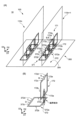
- FIG. 1 is a perspective view showing a configuration of a semiconductor module according to a first embodiment of the present invention
- 1 is a cross-sectional view showing a configuration of a semiconductor module according to a first embodiment of the present invention.
- 1A is an oblique view showing a group of inductors included in multiple memory chips according to a first embodiment of the present invention, and a group of inductors included in a magnetic field coupling chip-to-chip interface router chip (Through Chip Interface Router Chip (TCI router chip))
- FIG. 1B is an oblique view showing the configuration of the inductors on the memory chips and the inductors on the TCI router chip shown in FIG.
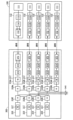
- 1 is a schematic diagram showing the configuration of a memory cube and a TCI router chip according to a first embodiment of the present invention
- 1 is a schematic diagram showing the configuration of a TCI router chip and a logic chip according to a first embodiment of the present invention
- 1 is a schematic diagram showing a configuration of a memory chip according to a first embodiment of the present invention
- 1 is a perspective view showing a configuration of a memory chip according to a first embodiment of the present invention
- 8 is a cross-sectional view showing the cross-sectional structure of the memory chip taken along the line A1-A2 shown in FIG. 7.
- 1 is a schematic diagram showing a configuration of a TCI router chip according to a first embodiment of the present invention
- 1 is a perspective view showing a configuration of a TCI router chip according to a first embodiment of the present invention
- 10 is a cross-sectional view showing the cross-sectional structure of the TCI router chip taken along line B1-B2 shown in FIG. 9.
- 1 is a schematic diagram showing a configuration of a logic chip according to a first embodiment of the present invention
- 1 is a perspective view showing a configuration of a logic chip according to a first embodiment of the present invention
- 13 is a cross-sectional view showing the cross-sectional structure of the logic chip taken along line C1-C2 shown in FIG. 12.
- FIG. 12 is a schematic diagram showing a configuration of a TCI router chip according to a first embodiment of the present invention
- 1 is a perspective view showing a configuration of a TCI router chip according to a first embodiment of the present invention
- 10 is a cross-sectional view showing
- FIG. 6 is a cross-sectional view showing a configuration of a semiconductor module according to a second embodiment of the present invention.
- FIG. 11 is a schematic diagram showing the configuration of a memory cube and a TCI router chip according to a second embodiment of the present invention.
- FIG. 11 is a cross-sectional view showing a configuration of a semiconductor module according to a third embodiment of the present invention.
- FIG. 11 is a schematic diagram showing the configuration of an FPGA cube and a TCI router chip according to a third embodiment of the present invention.
- FIG. 11 is a cross-sectional view showing a configuration of a semiconductor module according to a fourth embodiment of the present invention.
- FIG. 11 is a schematic diagram showing the configuration of a memory cube and a TCI router chip according to a second embodiment of the present invention.
- FIG. 11 is a cross-sectional view showing a configuration of a semiconductor module according to a third embodiment of the present invention.
- FIG. 11 is a schematic diagram showing the configuration
- FIG. 13 is a schematic diagram showing the configuration of a memory cube and a TCI router chip according to a fourth embodiment of the present invention.
- FIG. 13 is a cross-sectional view showing a configuration of a semiconductor module according to a fifth embodiment of the present invention.
- FIG. 13 is a cross-sectional view showing a configuration of a semiconductor module according to a sixth embodiment of the present invention.
- a certain component or region when a certain component or region is said to be "above (or below)" another component or region, unless otherwise specified, this includes not only the case where it is directly above (or below) the other component or region, but also the case where it is above (or below) the other component or region, i.e., the case where another component is included between the other component or region and above (or below) the other component or region.
- the D1 direction intersects with the D2 direction
- the D3 direction intersects with the D1 and D2 directions (D1D2 plane).
- the D1 direction is called the first direction
- the D2 direction is called the second direction
- the D3 direction is called the third direction.
- the terms “same” and “match” when the terms “same” and “match” are used, the terms “same” and “match” may include tolerances within the design range. In addition, in one embodiment of the present invention, when tolerances within the design range are included, the terms “approximately same” and “approximately match” may be used.
- FIG. 1 is a perspective view showing the configuration of the semiconductor module 10.
- FIG. 2 is a cross-sectional view showing the configuration of the semiconductor module 10.
- FIG. 3A is a perspective view showing an inductor group 171 included in a plurality of memory chips 110 included in the semiconductor module 10, and an inductor group 371 included in a magnetic field coupling chip-to-chip interface router chip (Through Chip Interface Router Chip (TCI router chip)) 300
- FIG. 3B is a perspective view showing the configuration of the inductor 172 on the memory chip 110 and the inductor 372 on the TCI router chip 300 shown in FIG. 3A.
- FIG. 4 is a schematic diagram showing the configuration of the memory cube 100 and the TCI router chip 300 included in the semiconductor module 10.
- FIG. 5 is a schematic diagram showing the configuration of the TCI router chip 300 and the logic chip 200 included in the semiconductor module 10.
- the semiconductor module 10 includes a memory cube 100, a TCI router chip 300, a logic chip 200, and an adhesive layer 400.
- the stack 20 is composed of the memory cube 100, the TCI router chip 300, the logic chip 200, and the adhesive layer 400.
- the semiconductor module 10 may include a bump layer 500, a package substrate 600, and a bump layer 700.
- the memory cube 100 may be referred to as a first semiconductor cube
- the TCI router chip 300 may be referred to as a first semiconductor chip
- the logic chip 200 may be referred to as a first logic chip.
- the memory cube 100 includes a configuration in which multiple memory chips 110 are stacked in the D1 direction. Each of the multiple memory chips 110 has a similar configuration including multiple inductors 172 (first inductors).
- the memory cube 100 includes a first surface 142 parallel to the D2 and D3 directions, and a second surface 144 that is opposite to the first surface 142 in the D1 direction and parallel to the first surface 142.
- the memory cube 100 also includes a first side surface 145 perpendicular to the first surface 142 and the second surface 144, a second side surface 146 adjacent to the first side surface 145, a third side surface 147 adjacent to the second side surface 146, and a fourth side surface 148 adjacent to the third side surface 147 and the first side surface 145.
- the memory cube 100 is disposed on the second surface 304 of the TCI router chip 300, with the second side 146 in contact with the adhesive layer 400 and facing the second surface 304 of the TCI router chip 300.
- the memory chip 110 may be referred to as a second semiconductor chip.
- the multiple inductors 172 are arranged in parallel to and spaced apart from the second side 146 and aligned in the D2 direction.
- the memory chips 110 When the multiple memory chips 110 are not distinguished from each other, the memory chips are expressed as memory chips 110. When the multiple memory chips 110 are distinguished from each other, the memory chips are expressed as memory chips 110n, memory chips 110n+1, etc.
- the multiple memory chips 110 included in the memory cube 100 include, for example, memory chip 110n (see FIG. 3) and memory chip 110n+1 (see FIG. 3) arranged adjacent to memory chip 110n. Note that the memory cube 100 includes a configuration in which eight layers of memory chips 110 are stacked in the D1 direction. The number of layers of memory chips 110 shown in FIG. 1 is an example, and the number of layers of memory chips 110 is not limited to the eight layers shown in FIG. 1. The number of layers of memory chips 110 may be appropriately selected based on the application, specifications, etc. of the semiconductor module 10.
- the TCI router chip 300 includes, for example, a transistor layer 330 and an inductor layer 370 laminated on the transistor layer 330.
- the transistor layer 330 includes a first surface 302, which is the exposed surface of the TCI router chip 300, and a plurality of through electrodes 360.
- the plurality of through electrodes 360 are exposed on the first surface 302.
- the inductor layer 370 includes a second surface 304, which is the exposed surface of the TCI router chip 300 opposite the first surface 302, and a plurality of inductors 372.
- the first surface 302 and the second surface 304 are parallel to the D1 direction and the D2 direction.
- the first surface 302 is positioned to face the second surface 204 of the logic chip 200 and is a surface that contacts the second surface 204 of the logic chip 200.
- the second surface 304 is in contact with the adhesive layer 400 and faces the second side surface 146 of the memory cube 100.
- the TCI router chip 300 includes a wiring layer 350 between the transistor layer 330 and the inductor layer 370.
- the transistor layer 330, the wiring layer 350, and the inductor layer 370 are stacked in this order in the D3 direction.
- the substrate 373 (see, for example, FIG. 11) included in the TCI router chip 300 is located downward (on the first surface 302 side) in the D3 direction, and the N-type transistor 368 and the P-type transistor 369 (see, for example, FIG. 11) are stacked above the substrate 373 in the D3 direction. That is, the stacking direction of each layer constituting the TCI router chip 300 is upward in the D3 direction.
- a mounting structure in which the stacking direction is upward in the D3 direction is called face-up mounting
- a mounting structure in which the stacking direction is downward in the D3 direction is called face-down mounting.
- the first surface 302 of the TCI router chip 300 is placed on the logic chip 200, and the TCI router chip 300 is mounted face-up.
- the logic chip 200 includes, for example, a lower wiring layer 210 and a transistor layer 230 stacked on the lower wiring layer 210.
- the lower wiring layer 210 includes a first surface 202, which is the exposed surface of the logic chip 200, a plurality of electrode pads 222, 221, and 220, and a plurality of wirings 228.
- the plurality of electrode pads 222, 221, and 220 are exposed on the first surface 202.
- the transistor layer 230 includes a second surface 204, which is the exposed surface of the logic chip 200 opposite the first surface 202, a plurality of through electrodes 260 connected to each of the plurality of wirings 228, and a plurality of wirings 280.
- the plurality of wirings 280 are exposed on the second surface 204.
- the first surface 202 and the second surface 204 are surfaces parallel to the D1 direction and the D2 direction.
- the second surface 204 is a surface that contacts the first surface 302 of the TCI router chip 300.
- the logic chip 200 is placed on the package substrate 600 via a bump layer 500 arranged on the first surface 202, for example.
- the second surface 204 of the logic chip 200 is arranged to face the first surface 302 of the TCI router chip 300, and the logic chip 200 is stacked (bonded) with the TCI router chip 300.
- each of the multiple wirings 280 is bonded to the corresponding multiple through electrodes 360, and the logic chip 200 is electrically connected to the TCI router chip 300.
- SDB silicon direct bonding
- the multiple wirings 280 and multiple through electrodes 360 are formed using, for example, a conductor made of a metal.
- the conductor made of a metal is, for example, a conductor containing copper.
- the wirings 280 and through electrodes 360 may be called, for example, a first electrode and a second electrode, respectively.
- the substrate 273 (see, for example, FIG. 14) included in the logic chip 200 is located below (on the first surface 202 side) in the direction D3, and the N-type transistor 268 and the P-type transistor 269 (see, for example, FIG. 14) are stacked above the substrate 273 in the direction D3.
- the first surface 202 of the logic chip 200 is disposed on the package substrate 600, and the logic chip 200 is mounted face-up on the package substrate 600.
- the adhesive layer 400 is disposed between the memory cube 100 and the TCI router chip 300, and bonds the memory cube 100 and the TCI router chip 300.
- the adhesive layer 400 may be, for example, an adhesive containing an epoxy resin or an acrylic polymer, a die bonding film (DBF) containing an epoxy resin or an acrylic polymer, or an adhesive film such as a die attached film (DAF).
- the package substrate 600 includes a multi-layer wiring structure in which wiring and insulating layers are alternately stacked.
- the package substrate 600 includes, for example, a second surface 604 and a first surface 602, which are exposed surfaces of the package substrate 600, and multiple wiring layers 608, 610, and 612.
- the wiring layers 608, 610, and 612 are arranged parallel to the D1 and D2 directions, and are stacked in this order from top to bottom in the D3 direction.
- the multiple wiring layers 608, 610, and 612 include multiple wirings 609, multiple wirings 611, and multiple wirings 613.
- the multiple wirings 609 are exposed on the first surface 602, and the multiple wirings 613 are exposed on the second surface 604.
- the wiring 609 is electrically connected to the wiring 611, and the wiring 611 is electrically connected to the wiring 613.
- the wiring and the insulating layers stacked alternately are omitted.
- the number of layers in the multilayer wiring structure of the package substrate 600 is not limited to the number of layers (three layers) shown in FIG. 2. The number of layers in the multilayer wiring structure of the package substrate 600 can be changed as appropriate based on the application or specifications of the semiconductor module 10.
- the package substrate 600 is electrically connected to the laminate 20 via a plurality of bumps 502 included in the bump layer 500 disposed between the laminate 20 and the package substrate 600.
- the package substrate 600 is also connected to an external substrate and an external circuit via a plurality of bumps 702 included in the bump layer 700.
- each of the plurality of wirings 609 exposed on the first surface 602 is electrically connected to each of the plurality of electrode pads 222, 221, and 220 included in the logic chip 200 using the bumps 502, and each of the plurality of wirings 613 exposed on the second surface 604 is connected to an external substrate and an external circuit using the bumps 702.
- the semiconductor module 10 includes a memory cube 100 suspended above a TCI router chip 300 in the D3 direction, and has a lower thermal resistance than a configuration including multiple memory chips stacked in the D1 and D2 directions. Therefore, the semiconductor module 10 has high thermal conductivity and excellent heat dissipation characteristics, making it possible to suppress malfunctions caused by temperature increases in the semiconductor module. Therefore, the limit on the number of stacked chips in the semiconductor module 10 is relaxed compared to a configuration including multiple memory chips stacked in the D1 and D2 directions.
- Memory chip 110n+1 includes an inductor layer 170 (see, for example, Figures 7 and 8).
- the inductor layer 170 includes multiple inductor groups 171, and each of the multiple inductor groups 171 includes multiple inductors 172.
- each of the multiple inductors 172 is arranged parallel to the D3 direction perpendicular to the D1 direction and the D2 direction (i.e., the second surface 304).
- the multiple inductors 172 are arranged parallel to and spaced apart from the second side surface 146 and lined up in the D2 direction.
- Each of the multiple inductors 372 includes terminal A, terminal B, a first portion 172a, a second portion 172b, a third portion 172c, a fourth portion 172d, and a fifth portion 172e.
- the inductor 172 is electrically connected to the transmission/reception circuit 114 ( Figure 4) using terminal A and terminal B.
- the fourth portion 172d extends in the D2 direction, one end of the fourth portion 172d is electrically connected to terminal A, and the other end of the fourth portion 172d is electrically connected to one end of the fifth portion 172e.
- the fifth portion 172e extends in the D3 direction, and the other end of the fifth portion 172e is electrically connected to one end of the first portion 172a.
- the first portion 172a extends in the D2 direction, and the other end of the first portion 172a is electrically connected to one end of the second portion 172b.
- the second portion 172b extends in the D3 direction, and the other end of the second portion 172b is electrically connected to one end of the third portion 172c.
- the third portion 172c extends in the D2 direction, and the other end of the third portion 172c is electrically connected to terminal B.
- the TCI router chip 300 includes an inductor group 371 including a plurality of inductors 372 arranged parallel to the position where the plurality of inductors 172 are arranged, and parallel to and adjacent to the second surface 304.
- the TCI router chip 300 includes an inductor layer 370 (see, for example, Figures 10 and 11), which includes a plurality of inductors 372.
- the plurality of inductors 372 are arranged in a matrix along the D1 direction and the D2 direction.
- Each of the plurality of inductors 372 includes a terminal C, a terminal D, a first portion 372a, a second portion 372b, a third portion 372c, a fourth portion 372d, and a fifth portion 372e.
- the inductors 372 are electrically connected to the transmission/reception circuit 314 using the terminals C and D, as will be described in detail later.
- the fourth portion 372d extends in the D2 direction, one end of the fourth portion 372d is electrically connected to terminal C, and the other end of the fourth portion 372d is electrically connected to one end of the fifth portion 372e.
- the fifth portion 372e extends in the D1 direction, and the other end of the fifth portion 372e is electrically connected to one end of the first portion 372a.
- the first portion 372a extends in the D2 direction, and the other end of the first portion 372a is electrically connected to one end of the second portion 372b.
- the second portion 372b extends in the D1 direction, and the other end of the second portion 372b is electrically connected to one end of the third portion 372c.
- the third portion 372c extends in the D2 direction, and the other end of the third portion 372c is electrically connected to terminal D.
- the shape of the inductor 172 when viewed from the D1 direction in a plane parallel to the D2 and D3 directions, and the shape of the inductor 372 when viewed from the D3 direction in a plane parallel to the D1 and D2 directions, are, for example, rectangular. Since the memory chip 110 stands perpendicular to the TCI router chip 300, the inductor 172 is disposed facing the inductor 372 at 90 degrees. Also, when viewed from the D3 direction in a plane parallel to the D1 and D2 directions, the first portion 172a of the inductor 172 overlaps the first portion 372a of the inductor 372.
- inductor 172 and inductor 372 that face each other are magnetically coupled, so that the inductors can communicate with each other one-to-one without contact.
- the communication between the inductors that occurs due to magnetic field coupling is called, for example, inductor communication, signal communication, data communication, etc.
- the shapes of inductor 172 and inductor 372 are not limited to a quadrangle.
- inductor 172 and inductor 372 may be trapezoidal or pentagonal.
- the shapes of inductor 172 and inductor 372 may be any shapes that allow inductor communication.
- inductor 172 and inductor 372 face each other at 90 degrees, and can communicate one-to-one by magnetic field coupling. More specifically, effective inductor communication is performed by first portion 172a of inductor 172 and first portion 372a of inductor 372.
- First portion 172a mainly has the function of performing inductor communication with first portion 372a.
- second portion 172b, third portion 172c, fourth portion 172d, and fifth portion 172e excluding first portion 172a mainly have the function of supplying current to first portion 172a.
- second portion 372b, third portion 372c, fourth portion 372d, and fifth portion 372e excluding first portion 372a mainly have the function of supplying current to first portion 372a in inductor 372.
- Inductor 372 has the same configuration and function as inductor 172. Note that in semiconductor module 10, viewing a surface parallel to the D2 and D3 directions from the D1 direction may be referred to as a front view, and viewing a surface parallel to the D1 and D2 directions from the D3 direction may be referred to as a planar view.
- the semiconductor module 10 includes a memory cube 100 suspended above a TCI router chip 300, and the overlapping portion of the inductor 172 and the inductor 372 is the first portion 172a and the first portion 372a, and the overlapping portion of the inductor 172 and the inductor 372 is minimized.
- the logic chip 200 does not include an inductor, and the inductor 172 in the memory cube 100 and the inductor 372 in the TCI router chip 300 are located away from the logic chip 200. Therefore, the semiconductor module 10 can suppress the generation of electromagnetic noise and the like due to inductor communication associated with the logic chip 200, and can suppress malfunctions associated with electromagnetic noise of the memory cube 100, the TCI router chip 300, and the logic chip 200.
- Circuit configuration of semiconductor module 10 The circuit configuration of the semiconductor module 10 will be described with reference to Fig. 4 and Fig. 5. As shown in Fig. 4, the memory cube 100 and the TCI router chip 300 are connected based on inductor communication. As shown in Fig. 4 or Fig. 5, the TCI router chip 300 and the logic chip 200 are electrically connected using a signal bus 340. Note that each circuit in the memory cube 100, each circuit in the TCI router chip 300, and each circuit in the logic chip 200 may be electrically connected using the signal bus 340.
- the memory cube 100 includes multiple Through Chip Interface-IOs (TCI-IOs) 112 and multiple memory modules 111.
- TCI-IOs Through Chip Interface-IOs
- the multiple TCI-IOs 112 are electrically connected to the memory modules 111.
- the TCI-IO 112 includes an inductor 172, a transmitting/receiving circuit 114, and a parallel-serial conversion circuit 113.
- the inductor 172 is electrically connected to the transmitting/receiving circuit 114 using terminals A and B.
- the transmitting/receiving circuit 114 is electrically connected to the parallel-serial conversion circuit 113.
- the parallel-serial conversion circuit 113 is electrically connected to the memory module 111.
- the inductor 172 has the function of non-contact inductor communication with the inductor 372 of the TCI router chip 300.
- the transmitting/receiving circuit 114 has, for example, a function of amplifying the signal (data) received by the inductor 172, and a function of removing noise from the received signal (data).
- the transmitting/receiving circuit 114 also has a function of transmitting the desired signal (data) converted using the parallel-serial conversion circuit 113 onto a radio wave.
- the signal received by the inductor 172 includes a large number of parallel signals (parallel signals) from the TCI router chip 300.
- the desired signal includes a large number of parallel signals (parallel signals) from the memory module 111.
- the parallel-serial conversion circuit 113 performs parallel-serial conversion on a number of parallel signals from the TCI router chip 300 to convert them into serial signals (serial signals).
- the serial signals are transferred at high speed using a single signal path (wiring).
- the parallel-serial conversion circuit 113 performs serial-parallel conversion on the serial signals just before the memory module 111 to return them to a number of parallel signals, and then transmits the number of parallel signals to the memory module 111.
- the parallel-serial conversion circuit 113 performs, for example, step 1 following step 2.
- the parallel-serial conversion circuit 113 is called, for example, a SerDes circuit (Serialize and Deserialize Circuit).
- the memory module 111 includes, for example, a function for generating a large number of parallel signals to be transmitted, and a function for controlling a large number of parallel signals received and storing them in the memory cell array 115 ( Figure 6).
- the TCI router chip 300 includes, for example, multiple TCI-IOs 312, multiple network routers (Router(R)) 318, multiple external IOs 316, and multiple memory controllers 319.
- TCI-IO 312, external IO 316, and memory controller 319 are functional blocks that make up an LSI (Large Scale Integration).
- the functional blocks that make up an LSI are called, for example, IP (Intellectual Property) cores, IPs, or macros.
- IP cores include a CPU (Central Processing Unit), a GPU (Graphics Processing Unit), memory, etc.
- IP cores such as multiple TCI-IOs 312, multiple external IOs 316, and multiple memory controllers 319 include a network interface (NI) 317.
- NI network interface
- IP cores such as the multiple TCI-IOs 312, multiple external IOs 316, and multiple memory controllers 319 may not include the NI 317, and the NI 317 may be located outside the multiple TCI-IOs 312, multiple external IOs 316, and multiple memory controllers 319, and each of the multiple TCI-IOs 312, multiple external IOs 316, and multiple memory controllers 319 may be electrically connected to the R318 corresponding to each circuit via the NI 317.
- IP cores such as multiple TCI-IOs 312, multiple external IOs 316, and multiple memory controllers 319 are electrically connected to R318s corresponding to the NIs 317 of each IP core.
- IP cores such as multiple TCI-IOs 312, multiple external IOs 316, and multiple memory controllers 319 are connected in a network using multiple R318s.
- the multiple R318s are electrically connected, for example, using multiple signal buses 340.
- the network configuration of the IP core using multiple R318 may be a mesh as shown in FIG. 5.
- the network configuration of the IP core shown in FIG. 5 is one example, and the network configuration of the IP core is not limited to the configuration shown in FIG. 5.
- the network configuration of the IP core is appropriately selected depending on the specifications and applications of the semiconductor module 10, the number of IP cores included in the semiconductor module 10, etc.
- the multiple TCI-IOs 312 include, for example, TCI-IOs 312a, 312b, ..., and 312e.
- TCI-IO312 When the multiple TCI-IOs 312 are not distinguished from one another, the TCI-IO is expressed as TCI-IO312.
- the multiple TCI-IOs 312 When the multiple TCI-IOs 312 are distinguished from one another, the multiple TCI-IOs are expressed as TCI-IOs 312a, 312b, ..., and 312e, etc. Note that there is no limit to the number of multiple TCI-IOs 312 included in the semiconductor module 10, and the number is appropriately selected depending on the specifications and applications of the semiconductor module 10, the number of IP cores included in the semiconductor module 10, and the like.
- TCI-IO312 includes an inductor 372, a transmitting/receiving circuit 314, a parallel-serial conversion circuit 313, and an NI317.
- the inductor 372 is electrically connected to the transmitting/receiving circuit 314 using terminals C and D.
- the transmitting/receiving circuit 314 is electrically connected to the parallel-serial conversion circuit 313.
- the parallel-serial conversion circuit 313 is electrically connected to NI317.
- TCI-IO312 (NI317) is electrically connected to R318.
- the configurations and functions of the inductor 372, the transmission/reception circuit 314, the parallel-serial conversion circuit 313, and the memory controller 319 are similar to those of the inductor 172, the transmission/reception circuit 114, the parallel-serial conversion circuit 113, and the memory module 111. Therefore, a description of the configurations and functions of the inductor 372, the transmission/reception circuit 314, the parallel-serial conversion circuit 313, and the memory controller 319 will be omitted here.
- NI 317 can convert, for example, data transmitted and received using signal bus 340 into a data format corresponding to an IP core electrically connected to NI 317, and can convert a data format corresponding to an IP core into a data format corresponding to signal bus 340.
- semiconductor module 10 can transmit and receive both addresses and data using signal bus 340, and therefore can have a smaller bus width than a module including signal buses arranged in a concentrated manner.
- semiconductor module 10 can transmit and receive data without relying on the data format corresponding to each IP core, and therefore can suppress an increase in the number of signal buses 340.
- the data transmitted and received using the signal bus 340 includes, for example, an address that can identify an IP core electrically connected to the NI 317.
- the multiple R318s include, for example, R318a, 318b, ... and 318i.
- the multiple Rs are expressed as R318.
- the multiple Rs are expressed as R318a, 318b, ... and 318i, etc.
- Each of the multiple R318 is electrically connected to the IP core and the signal bus 340.
- Each of the multiple R318 includes multiple switches, and can control the data transmission/reception path to each IP core connected in a network shape based on the address.
- the semiconductor module 10 can transmit and receive data to a desired IP core among the IP cores connected in a network shape by controlling the multiple switches of the multiple R318.
- the semiconductor module 10 can change the placement and address of R318 without depending on the placement of the IP core by controlling the data transmission/reception path to the IP core using R318, so that the data transmission/reception path can be flexibly set.
- R318 can also function as a repeater (also called a bus buffer) that aggregates multiple signal buses 340 and appropriately divides the routed signal buses 340. Therefore, the semiconductor module 10 can suppress the concentration of multiple signal buses 340. As a result, for example, the degree of freedom in the position of R318 is improved, and restrictions on the placement of IP cores connected to R318 can be relaxed.
- a repeater also called a bus buffer
- External IO316 includes, for example, NI317. External IO316 is electrically connected to R318 via NI317. External IO316 is electrically connected to logic chip 200, memory cube 100, and an external circuit (not shown, e.g., a power supply circuit) via R318, and has the function of transmitting and receiving signals between the external circuit and logic chip 200 and memory cube 100.
- external IO316 includes, for example, NI317.
- External IO316 is electrically connected to R318 via NI317.
- External IO316 is electrically connected to logic chip 200, memory cube 100, and an external circuit (not shown, e.g., a power supply circuit) via R318, and has the function of transmitting and receiving signals between the external circuit and logic chip 200 and memory cube 100.
- the memory controller 319 includes, for example, NI317.
- the memory controller 319 is electrically connected to R318 via NI317.
- the memory controller 319 is also electrically connected to the logic chip 200 and the memory cube 100 via R318, and has the function of transmitting and receiving signals between the memory cube 100 and the logic chip 200.
- the logic chip 200 includes, for example, multiple CPUs (Central Processing Units) 211, a memory interface 212, a PCIe interface (PCI Express Interface (PCIeIF)) 213, an Ethernet interface (Ethernet Interface (EIF)) 214, and multiple R218.
- CPUs Central Processing Units
- memory interface 212 a PCIe interface (PCI Express Interface (PCIeIF)) 213, an Ethernet interface (Ethernet Interface (EIF)) 214, and multiple R218.
- PCIeIF PCI Express Interface
- EIF Ethernet interface
- the multiple CPUs 211, memory interface 212, PCIeIF 213, and EIF 214 may be IP cores. Each of the multiple CPUs 211, memory interface 212, PCIeIF 213, and EIF 214 includes an NI 217.
- each of the multiple CPUs 211, memory interface 212, PCIeIF 213, and EIF 214 does not include NI 217, and NI 217 is located outside the multiple CPUs 211, memory interface 212, PCIeIF 213, and EIF 214, and each of the multiple CPUs 211, memory interface 212, PCIeIF 213, and EIF 214 may be electrically connected to R318 corresponding to each circuit via NI 217.
- the configuration and function of NI 217 are similar to those of NI 317. Therefore, a description of the configuration and function of NI 217 will be omitted here.
- the multiple IP cores such as CPU211, memory interface 212, PCIeIF213, and EIF214 are electrically connected to R218 corresponding to the NI217 of each IP core. Therefore, the multiple IP cores such as CPU211, memory interface 212, PCIeIF213, and EIF214 are connected in a network-like manner using multiple R218.
- the multiple R218 are electrically connected using, for example, multiple signal buses 340.
- the configuration and functions of the multiple R218 are similar to the configuration and functions of the multiple R318. Therefore, a description of the configuration and functions of the multiple R218 is omitted here.
- the multiple CPUs 211 include, for example, CPUs 211a, 211b, and 211c. When the multiple CPUs 211 are not distinguished from one another, the CPU is expressed as CPU 211. When the multiple CPUs 211 are distinguished from one another, the multiple CPUs are expressed as CPU 211a, 211b, and 211c, etc. There is no limit to the number of multiple CPUs 211 included in the semiconductor module 10, and the number is selected appropriately depending on the specifications and use of the semiconductor module 10, etc.
- the multiple R218s include, for example, R218a, 218b, ... and 218f.
- the multiple Rs are expressed as R218.
- the multiple Rs are expressed as R218a, 218b, ... and 218f, etc.
- the data transmitted and received using the signal bus 340 includes, for example, an address that can identify an IP core electrically connected to the NI 217.
- Each of the multiple CPUs 211 is a so-called logic module including an arithmetic circuit.
- Each of the multiple CPUs 211 has a function for controlling the transmission of signals (data) to the memory cube 100, the TCI router chip 300, the memory interface 212, the PCIeIF 213, the EIF 214, and the multiple R218, or the reception of signals (data) from the memory cube 100, the TCI router chip 300, the memory interface 212, the PCIeIF 213, the EIF 214, and the multiple R218.
- the CPU 211 transmits a signal for driving the memory module 111 via the TCI router chip 300.
- the memory interface 212 is, for example, a DRAM interface (Dynamic Random Access Memory (DRAM) IO) and has the function of transmitting and receiving signals between the DRAM (not shown) and the logic chip 200.
- DRAM Dynamic Random Access Memory
- the PCIeIF 213 is an interface that complies with the serial bus standard used, for example, to connect expansion cards within a computer.
- the PCIeIF 213 has the ability to transfer data at high speed with, for example, a CPU, memory, and storage connected to an expansion card installed in the computer.
- the EIF 214 is an interface that has the function of connecting, for example, the semiconductor module 10 and all devices (computers, printers, etc.) that communicate via the network to a network medium (cable).
- each circuit in the TCI router chip 300 and each circuit in the logic chip 200 are connected in a network via a network router (Router(R)), and each circuit in the memory cube 100 is connected to each circuit in the TCI router chip 300 and each circuit in the logic chip 200 using inductor communication.
- the semiconductor module 10 is a so-called network on chip (NoC) in which multiple IP cores are connected in a network, and is a module capable of communication using NoC and inductor communication.
- NoC network on chip
- R318h connected to the memory controller 319 is connected to R318g, R318e, and R318i in the TCI router chip 300, and is also connected to R218b in the logic chip 200. That is, the memory controller 319 connected to R318h is electrically connected to the memory controller 319 connected to R318g, the TCI-IO 312e connected to R318e, and the external IO 316 connected to R318i, and is also electrically connected to the PCIe IF 213 connected to R218b in the logic chip 200 via the signal bus 340.
- the TCI-IO 312e communicates with the inductor 172 in the memory cube 100 using the inductor 372, and is electrically connected to the memory module 111.
- R218b connected to PCIeIF213 is connected to R218a, R218c, and R218e in the logic chip 200. That is, PCIeIF213 connected to R218b is electrically connected to the memory interface 212 connected to R218a, the EIF214 connected to R218c, and the CPU 211b connected to R218e.
- CPU 211b transmits a signal for driving memory module 111 to TCI-IO 312e via R218e, R218b, signal bus 340, R318h and R318e, and TCI-IO 312e communicates with inductor 172 in memory cube 100 using inductor 372, and can transmit a signal for driving memory module 111 to memory module 111.
- the semiconductor module 10 electrically connects the TCI router chip 300 and the logic chip 200 using routers connected in a network, and is capable of communication using a network-type bus, as well as non-contact communication using inductor communication between the TCI router chip 300 and the memory cube 100 suspended from the TCI router chip 300.
- the semiconductor module 10 is a module that is three-dimensionally connected using electrical connections and connections based on non-contact communication, suppresses signal delays associated with wiring in the horizontal direction parallel to the D1 and D2 directions, and in the vertical direction (D3 direction), making it possible to reduce power consumption.
- Figure 6 is a schematic diagram showing the configuration of the memory chip 110.
- Figure 7 is a perspective view showing the configuration of the memory chip 110.
- Figure 8 is a cross-sectional view showing the schematic cross-sectional structure of the memory chip 110 taken along line A1-A2 shown in Figure 7. Configurations that are the same as or similar to those in Figures 1 to 5 will be described as necessary.
- the memory cube 100 includes a configuration in which multiple memory chips 110 are stacked in the D1 direction.
- the second side 146 is positioned so as to contact the adhesive layer 400 and face the second surface 304 of the TCI router chip 300, and the memory cube 100 is disposed on the second surface 304 of the TCI router chip 300.
- the memory chip 110 includes a plurality of memory modules 111, a plurality of TCI-IOs 112, power supply wiring 164, and ground wiring 165.
- Each of the plurality of memory modules 111 includes a memory cell array 115.
- Each of the plurality of TCI-IOs 112 includes a plurality of inductor groups 171, and the inductor groups 171 include a plurality of inductors 172.
- the memory chip 110 shown in FIG. 6 is, for example, an SRAM (Static Random Access Memory) chip.
- the memory module 111 has functions for controlling the storage of signals (data) in the memory cell array 115, the reading of signals (data) from the memory cell array 115, the transmission of signals (data) to the TCI-IO 112, and the reception of signals (data) from the TCI-IO 112.
- the memory cell array 115 includes a plurality of memory cells (not shown). Each of the plurality of memory cell arrays 115 is, for example, an SRAM, and each of the plurality of memory cells is an SRAM cell.
- the SRAM, SRAM cells, and memory module 111 for SRAM can employ technology used in the technical field of SRAM. Therefore, detailed explanations are omitted here.
- the plurality of memory cell arrays 115 and the plurality of memory cells may be memory cell arrays and memory cells other than SRAM, for example, DRAM (Dynamic Random Access Memory) and DRAM cells, MRAM (Magnetoresistive Random Access Memory) and MRAM cells, etc.
- the multiple memory modules 111 and the multiple TCI-IOs 112 are electrically connected to power supply wiring 164 and ground wiring 165.
- the power supply wiring 164 and ground wiring 165 are, for example, electrically connected to an external circuit (not shown), and are supplied with a power supply voltage VDD and a voltage VSS, etc.
- the power supply voltage VDD is, for example, 1 V, 3 V, etc.
- the voltage VSS is, for example, a ground voltage, 0 V, etc.
- each of the multiple memory chips 110 includes, for example, a transistor layer 130, a wiring layer 150, and an inductor layer 170.
- the multiple memory chips 110 include, for example, a memory chip 110n (FIG. 3(A)) and a memory chip 110n+1 (FIG. 3(A)) adjacent to the memory chip 110n.
- the memory chip 110 includes a first surface 102 parallel to the D2 and D3 directions, and a second surface 104 opposite the first surface 102 in the D1 direction.
- the first surface 102 is the exposed surface of the transistor layer 130.
- the second surface 104 is the exposed surface of the inductor layer 170.
- the first surface 102 and the second surface 104 are parallel to the first surface 142 and the second surface 144.
- the memory chip 110 also includes a first side 105 perpendicular to the first surface 102 and the second surface 104, a second side 106 adjacent to the first side 105, a third side 107 adjacent to the second side 106, and a fourth side 108 adjacent to the third side 107 and the first side 105.
- the first side 105 is part of the first side 145
- the second side 106 is part of the second side 146
- the third side 107 is part of the third side 147
- the fourth side 108 is part of the fourth side 148.
- a portion of the power supply wiring 164 and a portion of the ground wiring 165 are exposed, for example, on the first side 105, the fourth side 108, or the third side 107, and are electrically connected to side wiring that is electrically connected to an external circuit.
- the power supply voltage VDD and the voltage VSS are supplied to a portion of the power supply wiring 164 and a portion of the ground wiring 165 via the external circuit and the power side wiring.
- the side wiring can be formed by adopting technology used in the technical field of semiconductor modules.
- the inductor layer 170 includes a plurality of inductor groups 171.
- Each of the plurality of inductor groups 171 includes a plurality of inductors 172.
- the plurality of inductor groups 171 are arranged parallel to the D2 and D3 directions (i.e., the first surface 102 and the second surface 104) and perpendicular to the D1 and D2 directions.
- Each of the plurality of inductor groups 171 is arranged away from the fourth side surface 108 and close to the second side surface 146, and is arranged extending in the D2 direction. Note that although the number of inductors 172 shown in FIG. 7 is three, the number of inductors 172 shown in FIG. 7 is merely an example. The number of inductors 172 can be changed as appropriate depending on the specifications and applications of the semiconductor module 10.
- the multiple inductor groups 171 are adjacent to the second side 106 of the memory chip 110 and are arranged parallel to the D2 direction.
- Each of the multiple inductor groups 171 includes multiple inductors 172.
- the multiple inductors 172 include, for example, inductors having a data communication (data transmission) function and inductors having a clock communication (clock transmission) function.
- Each inductor 172 may perform inductor communication with its one-to-one corresponding inductor 372 in response to (synchronized with) a clock received by clock communication, or each inductor 172 may perform inductor communication with its one-to-one corresponding inductor 372 asynchronously (not synchronized with) the clock received by clock communication.
- each inductor 172 may perform inductor communication with its one-to-one corresponding inductor 372 asynchronously to the clock communication.
- the transistor layer 130 includes, for example, a substrate 173, wiring 163, insulating layer 174, fin 167, wiring 166, active region 184, gate insulating film 175, gate electrode 176, N-type transistor 168, P-type transistor 169, and insulating layer 177.
- the substrate 173 is, for example, an N-type Si substrate or an N-type Si-wafer.
- the memory chip 110 is formed by a 2 nm CMOS process and is configured using fin-type transistors as shown in FIG. 8, but may be formed by a CMOS process other than 2 nm and may be configured using transistors other than fin-type.
- the structure of the transistors of the memory chip 110 may be appropriately selected depending on the specifications and applications of the semiconductor module 10.
- the wiring layer 150 includes a multi-layer wiring structure in which wiring and insulating layers are alternately stacked.
- the wiring layer 150 includes, for example, wiring 178, insulating layer 179, wiring 180, and insulating layer 181.
- the number of layers of the multi-layer wiring in the wiring layer 150 is not limited to the two layers shown in FIG. 8.
- the number of layers of the multi-layer wiring in the wiring layer 150 may be three or more layers.
- the number of layers of the multi-layer wiring in the wiring layer 150 can be changed as appropriate depending on the specifications, applications, etc. of the semiconductor module 10.
- the inductor layer 170 includes, for example, an insulating layer 182 and a plurality of inductors 172.
- the inductor layer 170 also includes a plurality of inductor groups 171.
- Wiring 163 is a so-called buried electrode.
- Wiring 178 and wiring 166 are connected to an external circuit, for example, via the side wiring described above, and signals (data), power supply voltage VDD, voltage VSS, etc. are supplied to wiring 163 via the side wiring, wiring 178, and wiring 166.
- Wiring 178 and wiring 180 have, for example, a damascene structure, and wiring 166 has, for example, a structure equivalent to a through electrode.
- Inductor 172 is connected to wiring 180, which is connected to wiring 178.
- wiring 178 is electrically connected to the source electrode or drain electrode of N-type transistor 168, the source electrode or drain electrode of P-type transistor 169, gate electrode 176, and the like.
- a signal (data) received by inductor 172 is transmitted to N-type transistor 168, P-type transistor 169, and the like via wiring 180 and wiring 178.
- a signal (data) including the result of a logical operation is transmitted to inductor 172 via N-type transistor 168, P-type transistor 169, wiring 180, and wiring 178.
- Fig. 9 is a block diagram showing the configuration of the TCI router chip 300.
- Fig. 10 is a perspective view showing the configuration of the TCI router chip 300.
- Fig. 11 is a cross-sectional view showing an outline of the cross-sectional structure of the TCI router chip 300 taken along line B1-B2 shown in Fig. 10. Configurations that are the same as or similar to those in Figs. 1 to 8 will be described as necessary.
- the TCI router chip 300 includes a configuration in which a transistor layer 330, a wiring layer 350, and an inductor layer 370 are stacked in this order in the D3 direction, and includes a first surface 302 parallel to the D1 and D2 directions, and a second surface 304 opposite the first surface 302.
- the first surface 302 is the exposed surface of the transistor layer 330.
- the second surface 304 is the exposed surface of the inductor layer 370.
- the inductor layer 370 includes a plurality of inductor groups 371.
- the plurality of inductor groups 371 (see, for example, Fig. 3(A)) include a plurality of inductors 372.
- the plurality of inductors 372 are arranged in a matrix in parallel to the D1 direction and the D2 direction (i.e., the first surface 302 and the second surface 304).
- the transistor layer 330 includes, for example, a substrate 373, a wiring 363, a through electrode 360, a through electrode 394, a through electrode 395, an insulating layer 374, a fin 367, a wiring 366, an activation region 384, a gate insulating film 375, a gate electrode 376, an N-type transistor 368, a P-type transistor 369, and an insulating layer 377.
- the wiring layer 350 includes a multilayer wiring structure in which wiring and insulating layers are alternately stacked.
- the wiring layer 350 includes, for example, a wiring 378, an insulating layer 379, a wiring 380, and an insulating layer 381.
- the inductor layer 370 includes, for example, an insulating layer 382 and a plurality of inductors 372.
- substrate 373, wiring 363, insulating layer 374, fin 367, wiring 366, active region 384, gate insulating film 375, gate electrode 376, N-type transistor 368, P-type transistor 369, insulating layer 377, wiring 378, insulating layer 379, wiring 380, insulating layer 381, insulating layer 382, and inductor 372 are similar to the respective configurations and functions of substrate 173, wiring 163, insulating layer 174, fin 167, wiring 166, active region 184, gate insulating film 175, gate electrode 176, N-type transistor 168, P-type transistor 169, insulating layer 177, wiring 178, insulating layer 179, wiring 180, insulating layer 181, insulating layer 182, and inductor 172 described in "1-2. Overview of memory cube 100". Therefore, the layers and wiring that make up the transistor layer 330, wiring layer 350, and inductor layer 370 will be described as necessary.
- the through electrodes 360, 394, and 395 are electrically connected to wiring 363, which is a so-called embedded wiring, and a portion of the through electrodes 360, 394, and 395 are exposed on the first surface 302. A portion of the through electrodes 360, 394, and 395 are electrically connected to wiring 280 exposed on the second surface 204 of the logic chip 200. Signals (data), power supply voltage VDD, voltage VSS, etc. are supplied from an external circuit to the through electrodes 360, 394, and 395 via the logic chip 200 (e.g., wiring 280).
- the TCI router chip 300 includes, for example, multiple TCI-IOs 312, multiple R318s, multiple external IOs 316, and multiple memory controllers 319.
- the multiple TCI-IOs 312 include TCI-IOs 312a to 312e and TCI-IO 312j, and the multiple R318s include R318a to R318j.
- Each of the multiple TCI-IOs 312 includes multiple inductor groups 271, and the inductor group 271 includes multiple inductors 372.
- the configuration of the TCI router chip 300 shown in Figure 9 is an example, and the configuration of the TCI router chip 300 is not limited to the example shown in Figure 9.
- the TCI router chip 300 may include IP cores other than those shown in Figure 9.
- the power supply wiring 364 is electrically connected to the through electrode 394
- the ground wiring 365 is electrically connected to the through electrode 395
- the signal bus 340 (see FIG. 4) is electrically connected to the through electrode 360 (see FIG. 11).
- the TCI router chip 300 includes, as an example, one through electrode 394 and one through electrode 395, and includes one system of power supply wiring 364 and one system of ground wiring 365.
- the TCI router chip 300 includes, as an example, two through electrodes 360 and three systems of signal bus 340.
- the number of through electrodes 394, through electrodes 395, and through electrodes 360 included in the TCI router chip 300, and the number of systems of power supply wiring 364, ground wiring 365, and signal bus 340 are not limited to the examples shown in FIG. 11 or FIG. 5.
- the TCI router chip 300 may include two or more through electrodes 394, 395, and 360, and may include two or more power supply wiring 364, ground wiring 365, and signal bus 340.
- the number of through electrodes 394, 395, and 360 included in the TCI router chip 300, and the number of power supply wiring 364, ground wiring 365, and signal bus 340 systems can be changed as appropriate depending on the specifications and applications of the semiconductor module 10.
- the second surface 304 of the TCI router chip 300 is mounted on the adhesive layer 400, and the first surface 302 is mounted on the second surface 204 of the logic chip 200.
- the TCI router chip 300 is mounted face-up on the adhesive layer 400.
- the multiple inductors 372 arranged on the second surface 304 side are positioned away from the logic chip 200. This makes it possible to suppress the generation of electromagnetic noise and the like due to inductor communication associated with the logic chip 200.
- the multiple inductors 372 are arranged in a matrix in the D1 and D2 directions on the second surface 304 side.
- each inductor 372 may perform inductor communication with its one-to-one corresponding inductor 172 in response to (synchronized with) a clock received by clock communication, or may perform inductor communication with its one-to-one corresponding inductor 172 asynchronously (not synchronized with) the clock received by clock communication.
- Fig. 12 is a block diagram showing the configuration of logic chip 200.
- Fig. 13 is a perspective view showing the configuration of logic chip 200.
- Fig. 14 is a cross-sectional view showing an outline of the cross-sectional structure of logic chip 200 taken along line C1-C2 shown in Fig. 13. Configurations that are the same as or similar to those in Figs. 1 to 11 will be described as necessary.
- the logic chip 200 includes a configuration in which a lower wiring layer 210 and a transistor layer 230 are stacked in this order in the D3 direction as shown in FIG. 13, and includes a first surface 202 parallel to the D1 and D2 directions, and a second surface 204 opposite the first surface 202.
- the first surface 202 is the exposed surface of the lower wiring layer 210.
- the second surface 204 is the exposed surface of the transistor layer 230.
- the transistor layer 230 includes, for example, a substrate 273, wiring 263, through electrode 260, through electrode 294, through electrode 295, insulating layer 274, fin 267, wiring 266, active region 284, gate insulating film 275, gate electrode 276, N-type transistor 268, P-type transistor 269, and insulating layer 277.
- the transistor layer 230 also includes a multi-layer wiring structure in which wiring and insulating layers are alternately stacked.
- the multi-layer wiring structure includes, for example, wiring 278, insulating layer 279, wiring 280, and insulating layer 281.
- substrate 273, wiring 263, through electrode 260, through electrode 294, through electrode 295, insulating layer 274, fin 267, wiring 266, activation region 284, gate insulating film 275, gate electrode 276, N-type transistor 268, P-type transistor 269, insulating layer 277, wiring 278, insulating layer 279, wiring 280, and insulating layer 281 are similar to the respective configurations and functions of substrate 373, wiring 363, through electrode 360, through electrode 394, through electrode 395, insulating layer 374, fin 367, wiring 366, activation region 384, gate insulating film 375, gate electrode 376, N-type transistor 368, P-type transistor 369, insulating layer 377, wiring 378, insulating layer 379, wiring 380, insulating layer 381, and insulating layer 382 described in "1-3. Overview of TCI router chip 300". Therefore, each layer and wiring that constitutes the transistor layer 230 will be explained as necessary.
- the lower wiring layer 210 includes a multi-layer wiring structure in which wiring and insulating layers are alternately stacked.
- the lower wiring layer 210 includes, for example, electrode pad 220, electrode pad 221, electrode pad 222, insulating layer 223, through electrode 224, through electrode 225, through electrode 226, insulating layer 227, wiring 228, and insulating layer 229.
- the number of layers of the multi-layer wiring in the lower wiring layer 210 is not limited to two layers as shown in FIG. 14.
- the number of layers of the multi-layer wiring in the lower wiring layer 210 may be three or more layers.
- the number of layers of the multi-layer wiring in the lower wiring layer 210 can be changed as appropriate depending on the specifications, applications, etc. of the semiconductor module 10.
- the lower wiring layer 210 is a wiring layer for so-called backside power delivery (BPD).
- BPD is a technology used in the technical field of semiconductor modules, and a detailed explanation will be omitted here. Simply put, it is a technology that separates the supply of signals (data), power supply voltage, voltage, etc., on the second surface 204 side and the first surface 202 side of the substrate 273, respectively.
- the use of BPD makes it possible to scale the metal wiring connections inside the semiconductor module 10, simplifying complex metal wiring patterning and reducing the manufacturing costs of the semiconductor module 10.
- the through electrodes 260, 294, and 295 are electrically connected to the wiring 263, which is a so-called embedded wiring.
- the through electrodes 260, 294, and 295 are electrically connected to the wiring 228 of the second layer, for example, counting from the first surface 202 side.
- the second layer wiring 228 is electrically connected to the electrode pad 222, for example, using a plurality of through electrodes 226.
- the second layer wiring 228 is electrically connected to the electrode pad 221, for example, using a plurality of through electrodes 225, and is electrically connected to the electrode pad 220, for example, using a plurality of through electrodes 224.
- a power supply voltage VDD is supplied from an external circuit to the electrode pad 221
- a voltage VSS is supplied from an external circuit to the electrode pad 222
- a signal (data) is supplied from an external circuit to the electrode pad 220.
- signals (data), power supply voltage VDD, voltage VSS, etc. are supplied from an external circuit to through electrodes 226, 225, and 224 via the electrode pads, and are then supplied to the inside of logic chip 200.
- Electrode pad 220, electrode pad 221, and electrode pad 222 are the first layer of wiring counting from the first surface 202 side.
- logic chip 200 includes, for example, multiple CPUs 211, memory interface 212, PCIe IF 213, EIF 214, and multiple R218.
- the multiple CPUs 211 include CPUs 211a to 211c, and the multiple R218 include R218a to R318f.
- the configuration of logic chip 200 shown in Figure 12 is just an example, and the configuration of logic chip 200 is not limited to the example shown in Figure 12.
- logic chip 200 may include IP cores other than those shown in Figure 12.
- the CPU 211 has a function for controlling the transmission of signals (data) to the TCI-IO 312, or the reception of signals (data) from the TCI-IO 312.
- the CPU 211 also has a function for driving the memory module 111 in the memory chip 110.
- the CPU 211 transmits a signal for driving the memory module 111 via the TCI-IO 312.
- the CPU 211 is a logic module, and may include an arithmetic circuit such as a CPU (Central Processing Unit).
- the power supply wiring 264 is electrically connected to the electrode pad 221 via the through electrode 294, the wiring 228, and the multiple through electrodes 225, and the ground wiring 265 is electrically connected to the electrode pad 222 via the through electrode 295, the wiring 228, and the multiple through electrodes 226.
- the through electrode 360 (see FIG. 11) connected to the signal bus 340 (see FIG. 5) is electrically connected to the electrode pad 220 via the wiring 280, the wiring 278, the wiring 266, the wiring 263, the through electrode 260, the wiring 228, and the multiple through electrodes 224.
- the logic chip 200 includes, as an example, one each of the electrode pads 221, 222, and 220, and includes one each of the power supply wiring 264 and the ground wiring 265. As shown in FIG. 14 or 5, the logic chip 200 includes, as an example, one wiring 280, and includes three systems of the signal bus 340.
- the number of the electrode pads 221, 222, and 220 included in the logic chip 200, and the number of systems of the power supply wiring 264, the ground wiring 265, and the signal bus 340 are not limited to the examples shown in FIG. 12, 14, or 5.
- the logic chip 200 may include two or more each of the electrode pads 221, 222, and 220, and may include two or more systems of the power supply wiring 264, the ground wiring 265, and the signal bus 340.
- the number of electrode pads 221, electrode pads 222, and electrode pads 220 included in the logic chip 200, as well as the number of power supply wiring 264, ground wiring 265, and signal bus 340 systems, can be changed as appropriate depending on the specifications, applications, etc. of the semiconductor module 10.
- FIG. 15 is a cross-sectional view showing the configuration of the semiconductor module 10A.
- Figure 16 is a schematic diagram showing the configurations of a memory cube 100A and a TCI router chip 300A included in the semiconductor module 10A. Configurations that are the same as or similar to those in Figures 1 to 14 will be described as necessary.
- the semiconductor module 10A includes a memory cube 100A, a TCI router chip 300A, a logic chip 200, and an adhesive layer 400.
- the stack 20A is composed of the memory cube 100A, the TCI router chip 300A, the logic chip 200, and the adhesive layer 400.
- the semiconductor module 10A may include a bump layer 500, a package substrate 600, and a bump layer 700.
- the semiconductor module 10A includes a configuration in which the memory cube 100 and the TCI router chip 300 of the semiconductor module 10 are replaced with the memory cube 100A and the TCI router chip 300A.
- the configuration of the semiconductor module 10A other than the memory cube 100A and the TCI router chip 300A is the same as that of the semiconductor module 10. In the description of the semiconductor module 10A, the configuration similar to that of the semiconductor module 10 will be described as necessary.
- Memory cube 100A includes a configuration in which the multiple memory chips 110 of memory cube 100 are replaced with multiple DRAM chips 110A.
- the configuration of DRAM chip 110A is the same as the configuration of memory chip 110 described in the first embodiment, except that it is a DRAM.
- DRAM chip 110A includes multiple DRAMs 111A, multiple TCI-IOs 112, etc.
- memory cube 100A includes a configuration in which memory module 111 of memory cube 100 is replaced with DRAM 111A.
- the configuration of memory cube 100A other than the configuration related to DRAM 111A is the same as that of semiconductor module 10.
- DRAM 111A is electrically connected to TCI-IO 112 (parallel-serial conversion circuit 113).
- DRAM 111A includes functions such as generating a large number of parallel signals to transmit, and controlling a large number of parallel signals received and storing them in a memory cell array included in DRAM 111A.
- the TCI router chip 300A includes a configuration in which the memory controller 319 of the TCI router chip 300 is replaced with a DRAM controller 319A.
- the configuration of the TCI router chip 300A other than the configuration related to the DRAM controller 319A is the same as that of the semiconductor module 10.
- the DRAM controller 319A is electrically connected to R318.
- the DRAM controller 319A is, for example, an IP core.
- the DRAM controller 319A includes an NI317, similar to the memory controller 319. Note that the DRAM controller 319A does not include an NI317, and the NI317 may be located outside the DRAM controller 319A, and each of the multiple DRAM controllers 319A may be electrically connected to the R318 corresponding to each circuit via the NI317.
- IP cores such as multiple TCI-IO312, multiple external IO316, and multiple DRAM controllers 319A are electrically connected to R318 corresponding to the NI317 of each IP core.
- IP cores such as multiple TCI-IO312, multiple external IO316, and multiple DRAM controllers 319A are connected in a network using multiple R318.
- the multiple R318s are electrically connected using, for example, multiple signal buses 340.
- the DRAM controller 319A is electrically connected to the logic chip 200 and memory cube 100A via R318, and has the function of transmitting and receiving signals between the memory cube 100A and the logic chip 200.
- semiconductor module 10A can achieve the same effects as semiconductor module 10.
- semiconductor module 10A includes DRAM 111A and DRAM controller 319A, and has good thermal conductivity and excellent heat dissipation characteristics. As a result of suppressing malfunctions caused by electromagnetic noise and heat, it can transmit signals including large-capacity programs at high speed and with low power consumption compared to conventional semiconductor modules.
- FIG. 17 is a cross-sectional view showing the configuration of the semiconductor module 10B.
- Figure 18 is a schematic diagram showing the configurations of a memory cube 100B and a TCI router chip 300B included in the semiconductor module 10B. Configurations that are the same as or similar to those in Figures 1 to 16 will be described as necessary.
- the semiconductor module 10B includes a memory cube 100B, a TCI router chip 300B, a logic chip 200, and an adhesive layer 400.
- the stack 20B is composed of the memory cube 100B, the TCI router chip 300B, the logic chip 200, and the adhesive layer 400.
- the semiconductor module 10B may include a bump layer 500, a package substrate 600, and a bump layer 700.
- the semiconductor module 10B includes a configuration in which the memory cube 100 and the TCI router chip 300 of the semiconductor module 10 are replaced with the memory cube 100B and the TCI router chip 300B.
- the configuration of the semiconductor module 10B other than the memory cube 100B and the TCI router chip 300B is the same as that of the semiconductor module 10. In the description of the semiconductor module 10B, configurations similar to those of the semiconductor module 10 will be described as necessary.
- Memory cube 100B includes a configuration in which the multiple memory chips 110 of memory cube 100 are replaced with multiple FPGA (Field Programmable Gate Array) chips 110B.
- the configuration of FPGA chip 110B is the same as the configuration of memory chip 110 described in the first embodiment, except that it is an FPGA.
- FPGA chip 110B includes multiple FPGAs 111B, multiple TCI-IOs 112, etc.
- memory cube 100B includes a configuration in which memory module 111 of memory cube 100 is replaced with FPGA 111B.
- the configuration of memory cube 100B other than the configuration related to FPGA 111B is the same as that of semiconductor module 10.
- FPGA 111B is electrically connected to TCI-IO 112 (parallel-serial conversion circuit 113).
- FPGA 111B includes, for example, a function for generating a large number of parallel signals to be transmitted and a function for controlling a large number of parallel signals received.
- the TCI router chip 300B does not include the memory controller 319 of the TCI router chip 300. If the semiconductor module 10B includes a memory circuit having a function of storing data, such as a memory, it may include the memory controller 319. If the FPGA 111B includes a memory circuit, it may include the memory controller 319, and the FPGA 111B may include a configuration similar to that of the memory controller 319.
- the FPGA chip 110B is, for example, an IP core.
- IP cores such as multiple TCI-IO312 and multiple external IO316 are electrically connected to R318 corresponding to the NI317 of each IP core.
- IP cores such as multiple TCI-IO312 and multiple external IO316 are connected in a network using multiple R318.
- the multiple R318s are electrically connected using, for example, multiple signal buses 340.
- Semiconductor module 10B can achieve the same effects as semiconductor module 10.
- semiconductor module 10B has good thermal conductivity and excellent heat dissipation characteristics, suppresses malfunctions caused by electromagnetic noise and heat, and includes FPGA 111B that can be rewritten faster than conventional semiconductor modules.
- FIG. 19 is a cross-sectional view showing the configuration of the semiconductor module 10C.
- Figure 20 is a schematic diagram showing the configurations of a memory cube 100C and a TCI router chip 300C included in the semiconductor module 10C. Configurations that are the same as or similar to those in Figures 1 to 18 will be described as necessary.
- the semiconductor module 10C includes a memory cube 100C, a TCI router chip 300C, a logic chip 200, and an adhesive layer 400.
- the stack 20C is composed of the memory cube 100C, the TCI router chip 300C, the logic chip 200, and the adhesive layer 400.
- the semiconductor module 10C may include a bump layer 500, a package substrate 600, and a bump layer 700.
- the semiconductor module 10C includes a configuration in which the memory cube 100 and the TCI router chip 300 of the semiconductor module 10 are replaced with the memory cube 100C and the TCI router chip 300C.
- the configuration of the semiconductor module 10C other than the memory cube 100C and the TCI router chip 300C is the same as that of the semiconductor module 10. In the description of the semiconductor module 10C, configurations similar to those of the semiconductor module 10 will be described as necessary.
- the memory cube 100C includes a configuration in which the multiple memory chips 110 stacked in the D1 direction of the memory cube 100 are replaced with DRAM chips 110A and NVM (Non Volatile Memory) chips 110C stacked alternately in the D1 direction.
- the memory cube 100C includes DRAM chips 110A and NVM chips 110C stacked alternately.
- the configuration of the memory chip 110 described in the first embodiment is the same as that of the memory chip 110 described in the first embodiment except that the memory chip is the DRAM chip 110A
- the configuration of the NVM chip 110C is the same as that of the memory chip 110 described in the first embodiment except that the memory chip is the NVM.
- the DRAM chip 110A includes multiple DRAMs 111A, multiple TCI-IOs 112, etc.
- the NVM chip 110C includes multiple NVMs 111C, multiple TCI-IOs 112, etc.
- memory cube 100C includes a configuration in which memory module 111 of memory cube 100 is replaced with DRAM 111A and NVM 111C.
- the configuration of memory cube 100C other than that related to DRAM 111A and NVM 111C is the same as that of semiconductor module 10.
- DRAM 111A is electrically connected to TCI-IO 112 (parallel-serial conversion circuit 113)
- NVM 111C is electrically connected to TCI-IO 112 (parallel-serial conversion circuit 113) different from the TCI-IO 112 (parallel-serial conversion circuit 113) connected to DRAM 111A.
- DRAM 111A includes, for example, a function to generate a large number of parallel signals to be transmitted, and a function to control a large number of parallel signals received and store them in a memory cell array included in DRAM 111A.
- NVM 111C includes, for example, a function to generate a large number of parallel signals to be transmitted, and a function to control a large number of parallel signals received and store them in a memory cell array included in NVM 111C.
- the TCI router chip 300C includes a configuration in which the memory controller 319 of the TCI router chip 300 is replaced with a DRAM controller 319A and an NVM controller 319C.
- the configuration of the TCI router chip 300C other than the configuration related to the DRAM controller 319A and the NVM controller 319C is the same as that of the semiconductor module 10.
- the DRAM controller 319A is electrically connected to, for example, R318g
- the NVM controller 319C is electrically connected to, for example, R318h.
- the DRAM controller 319A and the NVM controller 319C are, for example, IP cores.
- the DRAM controller 319A and the NVM controller 319C include an NI 317, just like the memory controller 319. Note that the DRAM controller 319A and the NVM controller 319C do not include an NI 317, and the NI 317 is located outside the DRAM controller 319A and the NVM controller 319C, and each of the DRAM controller 319A and the NVM controller 319C may be electrically connected to the R318 corresponding to each circuit via the NI 317.
- IP cores such as multiple TCI-IOs 312, multiple external IOs 316, DRAM controller 319A, and NVM controller 319C are electrically connected to R318s corresponding to the NIs 317 of each IP core.
- IP cores such as multiple TCI-IOs 312, multiple external IOs 316, multiple DRAM controllers 319A, and NVM controller 319C are connected in a network using multiple R318s.
- the multiple R318s are electrically connected, for example, using multiple signal buses 340.
- the DRAM controller 319A and the NVM controller 319C are electrically connected to the logic chip 200 and the memory cube 100C via R318, and have the function of transmitting and receiving signals between the memory cube 100C and the logic chip 200.
- Semiconductor module 10C can achieve the same effects as semiconductor module 10.
- Semiconductor module 10C also includes DRAM 111A and DRAM controller 319A, which have good thermal conductivity and excellent heat dissipation characteristics, and are less susceptible to malfunctions caused by electromagnetic noise and heat, and can transmit signals including large-capacity programs at high speed and with low power consumption compared to conventional semiconductor modules.
- Semiconductor module 10C also includes NVM 111C and NVM controller 319C, which have good thermal conductivity and excellent heat dissipation characteristics, and are less susceptible to malfunctions caused by electromagnetic noise and heat, and can transmit signals including large-capacity data at high speed and with low power consumption compared to conventional semiconductor modules, and can store large-capacity data in a non-volatile manner.
- FIG. 21 is a cross-sectional view showing the configuration of the semiconductor module 10D. Configurations that are the same as or similar to those in Figs. 1 to 20 will be described as necessary.
- the semiconductor module 10D includes a memory cube 100D, a TCI router chip 300, a logic chip 200, a GPU (Graphics Processing Unit) 200A, and an adhesive layer 400.
- the stack 20D is composed of the memory cube 100D, the TCI router chip 300, the logic chip 200, and the adhesive layer 400.
- the semiconductor module 10D may include a bump layer 500, a package substrate 600, and a bump layer 700.
- the semiconductor module 10D includes a configuration in which the memory cube 100 of the semiconductor module 10 is replaced with the memory cube 100D, and the TCI router chip 300 on which the logic chip 200 of the semiconductor module 10 is stacked (bonded) is replaced with the TCI router chip 300 on which the logic chip 200 and the GPU 200A are stacked (bonded).
- the rest of the configuration of semiconductor module 10D is the same as that of semiconductor module 10 or semiconductor module 10A. In the description of semiconductor module 10D, configurations that are the same as those of semiconductor module 10 and semiconductor module 10A will be described as necessary.
- the multiple memory chips 110 stacked in the D1 direction of the memory cube 100 are one type of memory chip (SRAM).
- SRAM memory chip
- the multiple memory chips stacked in the D1 direction are two types: memory chip 110 and DRAM chip 110A.
- the memory chip 110 is an SRAM.
- the memory cube 100D includes a configuration in which two memory chips 110, four DRAM chips 110A, and two memory chips 110 are stacked in this order in the D1 direction.
- the stacking order of the memory chips 110 and DRAM chips 110A in the memory cube 100D is not limited to the example shown in FIG. 21.
- the stacking order of the memory chips 110 and DRAM chips 110A in the memory cube 100D can be changed as appropriate depending on the specifications, applications, etc. of the semiconductor module 10D.
- the configuration of the DRAM chip 110A is the same as the configuration of the memory chip 110 described in the second embodiment, except that it is a DRAM.
- the logic chip 200 and GPU 200A are stacked (bonded) to the TCI router chip 300.
- the stacking (bonding) of the logic chip 200 and the TCI router chip 300 is as described in "1-1-1.
- Overall configuration of the semiconductor module 10 is as described above.
- the GPU 200A includes a configuration in which the lower wiring layer 210A and the transistor layer 230A are stacked in this order in the D3 direction, and includes a first surface 202A parallel to the D1 and D2 directions, and a second surface 204A opposite to the first surface 202.
- the first surface 202A is the exposed surface of the lower wiring layer 210A.
- the second surface 204A is the exposed surface of the transistor layer 230A.
- the lower wiring layer 210A and the transistor layer 230A have the same configuration and function as the lower wiring layer 210 and the transistor layer 230 described in the first embodiment. Therefore, the configuration of the lower wiring layer 210A and the transistor layer 230A will be described as necessary.
- the transistor layer 230A includes a plurality of wirings 280, which are exposed to the second surface 204A, and the lower wiring layer 210A includes a plurality of electrode pads 220, which are exposed to the first surface 202A.
- GPU 200A includes the same configuration and functions as GPUs used in the technical field of semiconductor modules. For example, this is technology, and GPU 200A has the same configuration and functions as logic chip 200 and is a logic chip specialized for image processing. GPU 200A may be called a second logic chip.
- the first surface 202A of the GPU 200A is disposed on the package substrate 600, and the GPU 200A is mounted face-up on the package substrate 600.
- the first surface 302 of the TCI router chip 300 of the semiconductor module 10D is positioned to face the second surface 204A of the GPU 200A and is the surface that contacts the second surface 204A of the GPU 200A.
- each of the multiple through electrodes 360 exposed on the first surface 302 of the TCI router chip 300 is joined to a corresponding multiple number of multiple wirings 280 among the multiple wirings 280 exposed on the second surface 204, and the GPU 200A is electrically connected to the TCI router chip 300.
- each of the multiple wirings 609 exposed on the first surface 602 of the package substrate 600 is electrically connected to each of the multiple electrode pads 220 exposed on the first surface 202A of the GPU 200A using bumps 502, and each of the multiple wirings 613 exposed on the second surface 604 of the package substrate 600 is connected to an external substrate, an external circuit, etc. using bumps 702.
- the TCI router chip 300 may include a number of through electrodes 360 that are not connected to the logic chip 200 and the GPU 200A.
- the DRAM controller 319A and the NVM controller 319C are electrically connected to the logic chip 200 and the memory cube 100D via R318, and have the function of transmitting and receiving signals between the memory cube 100D and the logic chip 200.
- Semiconductor module 10D can achieve the same effects as semiconductor module 10.
- Semiconductor module 10D also includes a SARM chip and a DRAM chip 110A that have good thermal conductivity and excellent heat dissipation characteristics, and are suppressed from malfunctioning due to electromagnetic noise and heat, and can transmit signals including large-capacity programs and signals (data) at high speed and with low power consumption compared to conventional semiconductor modules.
- Semiconductor module 10D also includes a configuration that has good thermal conductivity and excellent heat dissipation characteristics, and is suppressed from malfunctioning due to electromagnetic noise and heat, and can transmit signals including signals (data) associated with image processing at high speed and with low power consumption.
- FIG. 22 is a cross-sectional view showing the configuration of the semiconductor module 10E. Configurations that are the same as or similar to those in Figs. 1 to 21 will be described as necessary.
- the semiconductor module 10E includes a memory cube 100A, a memory cube 100E, a TCI router chip 300, a logic chip 200, a GPU 200A, an adhesive layer 400A, and an adhesive layer 400.
- the stack 20E includes a memory cube 100A, a memory cube 100E, a TCI router chip 300, a logic chip 200, a GPU 200A, an adhesive layer 400A, and an adhesive layer 400.
- the semiconductor module 10E may include a bump layer 500, a package substrate 600, and a bump layer 700.
- the semiconductor module 10E includes a configuration in which the memory cube 100D of the semiconductor module 10D is replaced with a configuration in which the memory cube 100A and the memory cube 100E are connected by an adhesive layer 400A.
- the other configurations of the semiconductor module 10E are the same as those of the semiconductor module 10D. In the description of semiconductor module 10E, configurations similar to those of semiconductor module 10D will be described as necessary.
- the memory cube arranged in the D3 direction of the semiconductor module 10D is one level, memory cube 100D.
- the memory cube arranged in the D3 direction of the semiconductor module 10E is two levels, memory cube 100A and memory cube 100E.
- the memory cube arranged in the D3 direction of the semiconductor module 10E is two levels, but the memory cube arranged in the D3 direction of the semiconductor module 10E may be three or more levels.
- the number of levels of memory cubes arranged in the D3 direction of the semiconductor module 10E is appropriately selected depending on the specifications and applications of the semiconductor module 10E, the number of IP cores included in the semiconductor module 10, etc.
- the memory cube 100A has a similar configuration to the memory cube 100A according to the second embodiment.
- the reference numerals of the multiple inductors of the DRAM chip 110A included in the memory cube 100A are represented as inductors 172f to avoid duplication with the multiple inductors 172 included in the memory chip 110.
- the inductors 172f have the same configuration and function as the inductors 172.
- the multiple inductors 172f are arranged close to the second side surface 146 and extend in the D2 direction.
- the memory cube 100E includes a configuration in which the multiple memory chips 110 included in the memory cube 100A according to the second embodiment are replaced with multiple memory chips 110E.
- the memory chip 110E differs from the memory chip 110 in that the multiple inductors 172 included in the memory chip 110 are arranged close to both the second side surface 146 side and the fourth side surface 148 side, and are arranged extending in the D2 direction.
- the configuration and function of the inductors 172 included in the memory chip 110E are similar to the configuration and function of the inductors 172 included in the memory chip 110.
- the adhesive layer 400A is disposed between the fourth side 148 of the memory cube 100E and the second side 146D of the memory cube 100A, and bonds the memory cube 100E and the memory cube 100A.
- the adhesive layer 400A is formed of the same material as the adhesive layer 400.
- Each of the multiple inductors 172f is magnetically coupled to a corresponding inductor 172 among the multiple inductors 172 arranged adjacent to the fourth side 148 side, thereby enabling one-to-one non-contact communication between the inductors.
- each of the multiple inductors 172 arranged adjacent to the second side 146 side is magnetically coupled to a corresponding inductor 372 among the multiple inductors 372 arranged adjacent to the second surface 304 side of the TCI router chip 300, thereby enabling one-to-one non-contact communication between the inductors.
- semiconductor module 10E can achieve the same effects as semiconductor module 10.
- semiconductor module 10E includes a configuration in which memory cubes, in which memory chips are stacked in the D1 direction, are arranged in multiple stages in the D3 direction, and the memory capacity can be further increased.
- the various configurations of the semiconductor modules 10, 10A, 10B, 10C, 10D, and 10E illustrated as an embodiment of the present invention can be appropriately interchanged as long as they are not mutually inconsistent and do not deviate from the spirit of the present invention.
- the various configurations of the semiconductor modules 10, 10A, 10B, 10C, 10D, and 10E illustrated as an embodiment of the present invention can be appropriately combined as long as they are not mutually inconsistent and do not deviate from the spirit of the present invention.
- technical matters common to each embodiment are included in each embodiment even if not explicitly stated.
- 10 semiconductor module, 10A: semiconductor module, 10B: semiconductor module, 10C: semiconductor module, 10D: semiconductor module, 10E: semiconductor module, 20: stack, 20A: stack, 20B: stack, 20C: stack, 20D: stack, 20E: stack, 100: memory cube, 100A: memory cube, 100B: memory cube, 100C: memory cube, 100D: memory cube, 100E: memory cube, 102: first surface, 104: second surface, 105: first side, 106: second side, 107: third side, 108: fourth side, 110: memory chip, 110n: memory chip chip, 110n+1: memory chip, 110A: DRAM chip, 110B: FPGA chip, 110C: NVM chip, 111: memory module, 111A: DRAM, 111B: FPGA, 111C: NVM, 112: TCI-IO, 113: parallel-serial conversion circuit, 114: transmission/reception circuit, 115: memory cell array, 130: transistor layer, 142: first surface,
Landscapes
- Semiconductor Integrated Circuits (AREA)
Priority Applications (2)
| Application Number | Priority Date | Filing Date | Title |
|---|---|---|---|
| JP2025527597A JPWO2024262220A1 (https=) | 2023-06-20 | 2024-05-21 | |
| US19/405,996 US20260101828A1 (en) | 2023-06-20 | 2025-12-02 | Semiconductor module |
Applications Claiming Priority (2)
| Application Number | Priority Date | Filing Date | Title |
|---|---|---|---|
| JP2023-101092 | 2023-06-20 | ||
| JP2023101092 | 2023-06-20 |
Related Child Applications (1)
| Application Number | Title | Priority Date | Filing Date |
|---|---|---|---|
| US19/405,996 Continuation US20260101828A1 (en) | 2023-06-20 | 2025-12-02 | Semiconductor module |
Publications (1)
| Publication Number | Publication Date |
|---|---|
| WO2024262220A1 true WO2024262220A1 (ja) | 2024-12-26 |
Family
ID=93935672
Family Applications (1)
| Application Number | Title | Priority Date | Filing Date |
|---|---|---|---|
| PCT/JP2024/018676 Ceased WO2024262220A1 (ja) | 2023-06-20 | 2024-05-21 | 半導体モジュール |
Country Status (3)
| Country | Link |
|---|---|
| US (1) | US20260101828A1 (https=) |
| JP (1) | JPWO2024262220A1 (https=) |
| WO (1) | WO2024262220A1 (https=) |
Citations (12)
| Publication number | Priority date | Publication date | Assignee | Title |
|---|---|---|---|---|
| JPH03501428A (ja) * | 1987-10-20 | 1991-03-28 | アーヴィン・センサーズ・コーポレーション | 高密度電子モジュール及びその製造方法 |
| JPH0766371A (ja) * | 1993-08-19 | 1995-03-10 | Internatl Business Mach Corp <Ibm> | 垂直チップ・マウントのメモリ・パッケージ及びそれを製造する方法 |
| US5786628A (en) * | 1994-09-28 | 1998-07-28 | International Business Machines Corporation | Method and workpiece for connecting a thin layer to a monolithic electronic modules surface and associated module packaging |
| WO2009148007A1 (ja) * | 2008-06-03 | 2009-12-10 | 学校法人慶應義塾 | 電子回路 |
| JP2011044224A (ja) * | 2009-08-17 | 2011-03-03 | Numonyx Bv | 積層型デバイス構成のための近傍界結合を使用した高速ワイヤレス直列通信リンク |
| JP2011086738A (ja) * | 2009-10-15 | 2011-04-28 | Keio Gijuku | 積層半導体集積回路装置 |
| JP2011233842A (ja) * | 2010-04-30 | 2011-11-17 | Toshiba Corp | 不揮発性半導体記憶装置 |
| US20140223068A1 (en) * | 2005-09-26 | 2014-08-07 | Rambus Inc. | Memory System Topologies Including A Buffer Device And An Integrated Circuit Memory Device |
| JP2015502664A (ja) * | 2011-12-02 | 2015-01-22 | インテル・コーポレーション | デバイス相互接続の変化を可能にする積層メモリ |
| US20150357306A1 (en) * | 2012-12-23 | 2015-12-10 | Advanced Micro Devices, Inc. | Die-stacked device with partitioned multi-hop network |
| WO2021095083A1 (ja) * | 2019-11-11 | 2021-05-20 | ウルトラメモリ株式会社 | 半導体モジュール、dimmモジュール、及びそれらの製造方法 |
| WO2024057707A1 (ja) * | 2022-09-12 | 2024-03-21 | 先端システム技術研究組合 | 半導体モジュール及びその製造方法 |
-
2024
- 2024-05-21 WO PCT/JP2024/018676 patent/WO2024262220A1/ja not_active Ceased
- 2024-05-21 JP JP2025527597A patent/JPWO2024262220A1/ja active Pending
-
2025
- 2025-12-02 US US19/405,996 patent/US20260101828A1/en active Pending
Patent Citations (12)
| Publication number | Priority date | Publication date | Assignee | Title |
|---|---|---|---|---|
| JPH03501428A (ja) * | 1987-10-20 | 1991-03-28 | アーヴィン・センサーズ・コーポレーション | 高密度電子モジュール及びその製造方法 |
| JPH0766371A (ja) * | 1993-08-19 | 1995-03-10 | Internatl Business Mach Corp <Ibm> | 垂直チップ・マウントのメモリ・パッケージ及びそれを製造する方法 |
| US5786628A (en) * | 1994-09-28 | 1998-07-28 | International Business Machines Corporation | Method and workpiece for connecting a thin layer to a monolithic electronic modules surface and associated module packaging |
| US20140223068A1 (en) * | 2005-09-26 | 2014-08-07 | Rambus Inc. | Memory System Topologies Including A Buffer Device And An Integrated Circuit Memory Device |
| WO2009148007A1 (ja) * | 2008-06-03 | 2009-12-10 | 学校法人慶應義塾 | 電子回路 |
| JP2011044224A (ja) * | 2009-08-17 | 2011-03-03 | Numonyx Bv | 積層型デバイス構成のための近傍界結合を使用した高速ワイヤレス直列通信リンク |
| JP2011086738A (ja) * | 2009-10-15 | 2011-04-28 | Keio Gijuku | 積層半導体集積回路装置 |
| JP2011233842A (ja) * | 2010-04-30 | 2011-11-17 | Toshiba Corp | 不揮発性半導体記憶装置 |
| JP2015502664A (ja) * | 2011-12-02 | 2015-01-22 | インテル・コーポレーション | デバイス相互接続の変化を可能にする積層メモリ |
| US20150357306A1 (en) * | 2012-12-23 | 2015-12-10 | Advanced Micro Devices, Inc. | Die-stacked device with partitioned multi-hop network |
| WO2021095083A1 (ja) * | 2019-11-11 | 2021-05-20 | ウルトラメモリ株式会社 | 半導体モジュール、dimmモジュール、及びそれらの製造方法 |
| WO2024057707A1 (ja) * | 2022-09-12 | 2024-03-21 | 先端システム技術研究組合 | 半導体モジュール及びその製造方法 |
Also Published As
| Publication number | Publication date |
|---|---|
| JPWO2024262220A1 (https=) | 2024-12-26 |
| US20260101828A1 (en) | 2026-04-09 |
Similar Documents
| Publication | Publication Date | Title |
|---|---|---|
| US11693801B2 (en) | Stacked semiconductor device assembly in computer system | |
| US10090280B2 (en) | Microelectronic package including microelectronic elements having stub minimization for wirebond assemblies without windows | |
| KR102716191B1 (ko) | 반도체 메모리 장치 및 이를 구비하는 메모리 모듈 | |
| TW202101726A (zh) | 具有中介件的堆疊半導體封裝件 | |
| US20250210514A1 (en) | Semiconductor module | |
| CN101350345A (zh) | 半导体器件 | |
| CN103579209A (zh) | 用于dram在gpu之上的可替换3d堆叠方案 | |
| WO2024127812A1 (ja) | 半導体モジュール | |
| CN121335525A (zh) | 针对顶部逻辑半导体系统的直通电力输送 | |
| WO2024262220A1 (ja) | 半導体モジュール | |
| WO2024258852A1 (en) | Apparatus including tsv structure | |
| KR20250166521A (ko) | 적층된 메모리 칩들을 포함하는 메모리 스택 및 메모리 미디어 | |
| WO2024262221A1 (ja) | 半導体モジュール | |
| TW202406085A (zh) | 可配置為二維系統或三維系統的同質性小晶片 | |
| US20250118719A1 (en) | Chip package with multiple hbm stacks | |
| CN121368138A (zh) | 半导体结构、存储芯片和电子设备 | |
| TW202406088A (zh) | 半導體封裝及其製造方法 | |
| TW202505744A (zh) | 系統單晶片、半導體裝置以及輸入和輸出電路 | |
| CN113224021A (zh) | 半导体封装件 |
Legal Events
| Date | Code | Title | Description |
|---|---|---|---|
| 121 | Ep: the epo has been informed by wipo that ep was designated in this application |
Ref document number: 24825627 Country of ref document: EP Kind code of ref document: A1 |
|
| ENP | Entry into the national phase |
Ref document number: 2025527597 Country of ref document: JP Kind code of ref document: A |
|
| NENP | Non-entry into the national phase |
Ref country code: DE |