WO2024262175A1 - 冷却器、半導体装置、及び車両 - Google Patents
冷却器、半導体装置、及び車両 Download PDFInfo
- Publication number
- WO2024262175A1 WO2024262175A1 PCT/JP2024/017198 JP2024017198W WO2024262175A1 WO 2024262175 A1 WO2024262175 A1 WO 2024262175A1 JP 2024017198 W JP2024017198 W JP 2024017198W WO 2024262175 A1 WO2024262175 A1 WO 2024262175A1
- Authority
- WO
- WIPO (PCT)
- Prior art keywords
- top plate
- fins
- cooler
- refrigerant
- view
- Prior art date
- Legal status (The legal status is an assumption and is not a legal conclusion. Google has not performed a legal analysis and makes no representation as to the accuracy of the status listed.)
- Ceased
Links
Images








Classifications
-
- H—ELECTRICITY
- H05—ELECTRIC TECHNIQUES NOT OTHERWISE PROVIDED FOR
- H05K—PRINTED CIRCUITS; CASINGS OR CONSTRUCTIONAL DETAILS OF ELECTRIC APPARATUS; MANUFACTURE OF ASSEMBLAGES OF ELECTRICAL COMPONENTS
- H05K7/00—Constructional details common to different types of electric apparatus
- H05K7/20—Modifications to facilitate cooling, ventilating, or heating
-
- H—ELECTRICITY
- H10—SEMICONDUCTOR DEVICES; ELECTRIC SOLID-STATE DEVICES NOT OTHERWISE PROVIDED FOR
- H10D—INORGANIC ELECTRIC SEMICONDUCTOR DEVICES
- H10D80/00—Assemblies of multiple devices comprising at least one device covered by this subclass
- H10D80/30—Assemblies of multiple devices comprising at least one device covered by this subclass the at least one device being covered by groups H10D84/00 - H10D86/00, e.g. assemblies comprising integrated circuit processor chips
-
- H—ELECTRICITY
- H10—SEMICONDUCTOR DEVICES; ELECTRIC SOLID-STATE DEVICES NOT OTHERWISE PROVIDED FOR
- H10W—GENERIC PACKAGES, INTERCONNECTIONS, CONNECTORS OR OTHER CONSTRUCTIONAL DETAILS OF DEVICES COVERED BY CLASS H10
- H10W40/00—Arrangements for thermal protection or thermal control
- H10W40/10—Arrangements for heating
-
- H—ELECTRICITY
- H10—SEMICONDUCTOR DEVICES; ELECTRIC SOLID-STATE DEVICES NOT OTHERWISE PROVIDED FOR
- H10W—GENERIC PACKAGES, INTERCONNECTIONS, CONNECTORS OR OTHER CONSTRUCTIONAL DETAILS OF DEVICES COVERED BY CLASS H10
- H10W40/00—Arrangements for thermal protection or thermal control
- H10W40/40—Arrangements for thermal protection or thermal control involving heat exchange by flowing fluids
-
- H—ELECTRICITY
- H10—SEMICONDUCTOR DEVICES; ELECTRIC SOLID-STATE DEVICES NOT OTHERWISE PROVIDED FOR
- H10W—GENERIC PACKAGES, INTERCONNECTIONS, CONNECTORS OR OTHER CONSTRUCTIONAL DETAILS OF DEVICES COVERED BY CLASS H10
- H10W40/00—Arrangements for thermal protection or thermal control
- H10W40/40—Arrangements for thermal protection or thermal control involving heat exchange by flowing fluids
- H10W40/47—Arrangements for thermal protection or thermal control involving heat exchange by flowing fluids by flowing liquids, e.g. forced water cooling
-
- H—ELECTRICITY
- H10—SEMICONDUCTOR DEVICES; ELECTRIC SOLID-STATE DEVICES NOT OTHERWISE PROVIDED FOR
- H10W—GENERIC PACKAGES, INTERCONNECTIONS, CONNECTORS OR OTHER CONSTRUCTIONAL DETAILS OF DEVICES COVERED BY CLASS H10
- H10W40/00—Arrangements for thermal protection or thermal control
- H10W40/70—Fillings or auxiliary members in containers or in encapsulations for thermal protection or control
- H10W40/77—Auxiliary members characterised by their shape
-
- H—ELECTRICITY
- H10—SEMICONDUCTOR DEVICES; ELECTRIC SOLID-STATE DEVICES NOT OTHERWISE PROVIDED FOR
- H10W—GENERIC PACKAGES, INTERCONNECTIONS, CONNECTORS OR OTHER CONSTRUCTIONAL DETAILS OF DEVICES COVERED BY CLASS H10
- H10W90/00—Package configurations
-
- H—ELECTRICITY
- H10—SEMICONDUCTOR DEVICES; ELECTRIC SOLID-STATE DEVICES NOT OTHERWISE PROVIDED FOR
- H10W—GENERIC PACKAGES, INTERCONNECTIONS, CONNECTORS OR OTHER CONSTRUCTIONAL DETAILS OF DEVICES COVERED BY CLASS H10
- H10W72/00—Interconnections or connectors in packages
- H10W72/851—Dispositions of multiple connectors or interconnections
- H10W72/853—On the same surface
- H10W72/871—Bond wires and strap connectors
-
- H—ELECTRICITY
- H10—SEMICONDUCTOR DEVICES; ELECTRIC SOLID-STATE DEVICES NOT OTHERWISE PROVIDED FOR
- H10W—GENERIC PACKAGES, INTERCONNECTIONS, CONNECTORS OR OTHER CONSTRUCTIONAL DETAILS OF DEVICES COVERED BY CLASS H10
- H10W72/00—Interconnections or connectors in packages
- H10W72/851—Dispositions of multiple connectors or interconnections
- H10W72/874—On different surfaces
- H10W72/884—Die-attach connectors and bond wires
-
- H—ELECTRICITY
- H10—SEMICONDUCTOR DEVICES; ELECTRIC SOLID-STATE DEVICES NOT OTHERWISE PROVIDED FOR
- H10W—GENERIC PACKAGES, INTERCONNECTIONS, CONNECTORS OR OTHER CONSTRUCTIONAL DETAILS OF DEVICES COVERED BY CLASS H10
- H10W72/00—Interconnections or connectors in packages
- H10W72/851—Dispositions of multiple connectors or interconnections
- H10W72/874—On different surfaces
- H10W72/886—Die-attach connectors and strap connectors
-
- H—ELECTRICITY
- H10—SEMICONDUCTOR DEVICES; ELECTRIC SOLID-STATE DEVICES NOT OTHERWISE PROVIDED FOR
- H10W—GENERIC PACKAGES, INTERCONNECTIONS, CONNECTORS OR OTHER CONSTRUCTIONAL DETAILS OF DEVICES COVERED BY CLASS H10
- H10W90/00—Package configurations
- H10W90/701—Package configurations characterised by the relative positions of pads or connectors relative to package parts
- H10W90/731—Package configurations characterised by the relative positions of pads or connectors relative to package parts of die-attach connectors
- H10W90/734—Package configurations characterised by the relative positions of pads or connectors relative to package parts of die-attach connectors between a chip and a stacked insulating package substrate, interposer or RDL
-
- H—ELECTRICITY
- H10—SEMICONDUCTOR DEVICES; ELECTRIC SOLID-STATE DEVICES NOT OTHERWISE PROVIDED FOR
- H10W—GENERIC PACKAGES, INTERCONNECTIONS, CONNECTORS OR OTHER CONSTRUCTIONAL DETAILS OF DEVICES COVERED BY CLASS H10
- H10W90/00—Package configurations
- H10W90/701—Package configurations characterised by the relative positions of pads or connectors relative to package parts
- H10W90/751—Package configurations characterised by the relative positions of pads or connectors relative to package parts of bond wires
- H10W90/754—Package configurations characterised by the relative positions of pads or connectors relative to package parts of bond wires between a chip and a stacked insulating package substrate, interposer or RDL
-
- H—ELECTRICITY
- H10—SEMICONDUCTOR DEVICES; ELECTRIC SOLID-STATE DEVICES NOT OTHERWISE PROVIDED FOR
- H10W—GENERIC PACKAGES, INTERCONNECTIONS, CONNECTORS OR OTHER CONSTRUCTIONAL DETAILS OF DEVICES COVERED BY CLASS H10
- H10W90/00—Package configurations
- H10W90/701—Package configurations characterised by the relative positions of pads or connectors relative to package parts
- H10W90/761—Package configurations characterised by the relative positions of pads or connectors relative to package parts of strap connectors
- H10W90/764—Package configurations characterised by the relative positions of pads or connectors relative to package parts of strap connectors between a chip and a stacked insulating package substrate, interposer or RDL
Definitions
- the present invention relates to a cooler, a semiconductor device, and a vehicle.
- Some semiconductor devices used in power conversion devices such as inverter devices are equipped with a cooler that circulates a coolant to dissipate heat generated by semiconductor elements.
- This type of cooler has multiple fins in the flow path that circulates the coolant (for example, Patent Documents 1 to 5).
- Patent No. 3469475 specification JP 2018-207017 A Patent No. 5901343 specification Patent No. 6138197 specification Patent No. 3236137 specification
- the present invention was made in consideration of these points, and one of its objectives is to improve the cooling performance of coolers applied to semiconductor devices.
- the cooler of one embodiment of the present invention comprises a top plate having a heat dissipation surface formed on a first surface thereof, a bottom plate arranged opposite the top plate and thicker than the top plate, a plurality of fins connected to at least the top plate, and a peripheral wall portion formed between the top plate and the bottom plate to surround the outer periphery of the plurality of fins, and a flow path of the refrigerant is formed by a space surrounded by the top plate, the bottom plate, the plurality of fins, and the peripheral wall portion, and a heat dissipation surface is provided on the top plate, the bottom plate, or the peripheral wall portion at one end side in a first direction of the flow path of the refrigerant.
- each of the multiple fins includes an inclined portion that, in a first plan view when viewed from a second direction perpendicular to the first direction, extends in a direction displaced toward the refrigerant inlet as it moves away from the first surface of the top plate, and, in a second plan view when viewed from the first direction, extends in a direction displaced in the second direction as it moves away from the first surface of the top plate.
- the present invention can improve the cooling performance of a cooler applied to a semiconductor device.
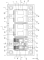
- 1 is a top view illustrating a configuration example of a semiconductor device according to an embodiment
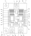
- 2 is an enlarged top view of a configuration of one circuit forming portion in the semiconductor device of FIG. 1
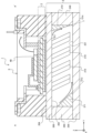
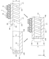
- 2 is a cross-sectional side view showing a configuration example of a semiconductor device taken along line A-A' in FIG. 1.
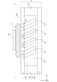
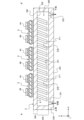
- 2 is a cross-sectional side view showing an example of the configuration of a semiconductor device taken along line B-B' in FIG. 1.
- 2 is a diagram illustrating an example of a circuit configuration of an inverter device to which the semiconductor device of FIG. 1 is applied.
- 1 is a bottom view illustrating a specific example of a fin in a cooler according to an embodiment.
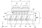
- FIG. 2 is a diagram illustrating a first characteristic of a refrigerant flow in a cooler according to an embodiment.
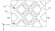
- FIG. 11 is a diagram illustrating a second characteristic of the flow of refrigerant in the cooler according to the embodiment.
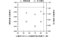
- FIG. 4 is a graph illustrating the relationship between the angle of the fin extension direction and the thermal resistance and pressure loss.
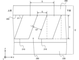
- FIG. 13 is a diagram for supplementing the angle and arrangement of the extension direction of the fins.
- FIG. 11 is a cross-sectional side view illustrating a first modified example of the configuration of the cooler.
- FIG. 11 is a cross-sectional side view illustrating a first modified example of the fin arrangement.
- FIG. 11 is a cross-sectional side view illustrating a second modified example of the fin arrangement.
- FIG. 11 is a cross-sectional side view showing a first modified example of the configuration of the cooler and the positional relationship between the inlet and outlet of the refrigerant.
- FIG. 11 is a cross-sectional side view showing a second modified example of the configuration of the cooler and the positional relationship between the inlet and outlet of the refrigerant.
- FIG. 11 is a cross-sectional side view showing a third modified example of the configuration of the cooler and the positional relationship between the inlet and outlet of the refrigerant.
- 1 is a schematic plan view showing an example of a vehicle to which a semiconductor device according to the present invention is applied;
- the X-axis, Y-axis, and Z-axis in each of the referenced drawings are shown for the purpose of defining planes and directions in the illustrated semiconductor device, cooler, etc.
- the X-axis, Y-axis, and Z-axis are mutually perpendicular and form a right-handed system.
- the direction parallel to the X-axis is called the X-direction
- the direction parallel to the Y-axis is called the Y-direction
- the direction parallel to the Z-axis is called the Z-direction.
- the Z direction may be referred to as the up-down direction.
- "up” and “above” are intended to mean the positive side of the Z direction relative to a reference surface, member, position, etc.
- “down” and “below” are intended to mean the negative side of the Z direction relative to a reference surface, member, position, etc.
- member B is placed on member A
- member B is placed on the positive side of the Z direction as viewed from member A.
- the top surface of member A this surface is the surface located at the end of member A on the positive side of the Z direction and facing the positive side of the Z direction.
- top view is intended to mean a planar view of the target item (e.g., a semiconductor device, a cooler, etc.) when viewed from the positive side of the Z direction
- bottom view is intended to mean a planar view of the target item when viewed from the negative side of the Z direction.
- front view is intended to mean a planar view of the target item when viewed from the negative side of the Y direction.
- side view refers to a planar view of the target object when viewed from the negative side in the X direction or the positive side in the X direction.
- a planar view when viewed from the negative side in the X direction is sometimes called a "left side view,” and a planar view when viewed from the positive side in the X direction is sometimes called a "right side view.”
- These directions and faces are terms used for convenience of explanation, and the corresponding relationship with each of the directions of the X axis, Y axis, and Z axis may change depending on the mounting posture of the semiconductor device.
- the surface on which the wiring board and semiconductor element of the cooler are arranged is called the upper surface of the cooler in this specification, but it may also be called the lower surface, side surface, etc. of the cooler.
- the semiconductor device exemplified in the following description may be applied to a power conversion device such as an inverter device for industrial or electrical equipment (e.g., an in-vehicle motor).
- a power conversion device such as an inverter device for industrial or electrical equipment (e.g., an in-vehicle motor).
- FIG. 1 is a top view showing an example of the configuration of a semiconductor device according to one embodiment.
- FIG. 2 is a top view showing an enlarged configuration of one circuit formation portion in the semiconductor device of FIG. 1.
- FIG. 3 is a cross-sectional side view showing an example of the configuration of a semiconductor device cut along line A-A' in FIG. 1.
- FIG. 4 is a cross-sectional side view showing an example of the configuration of a semiconductor device cut along line B-B' in FIG. 1.
- the cross-sectional side view of FIG. 3 shows a right side view of a portion of the semiconductor device cut along line A-A' in FIG. 1 to the left of line A-A'.
- FIG. 4 shows a front view of a portion of the semiconductor device cut along line B-B' in FIG. 1 to the upper side of line B-B'. Note that in FIGS. 2 and 3, the sealant that seals the semiconductor element and the like is omitted, and in FIG. 4, the leads, case, sealant, and the like are omitted.
- the semiconductor device 1 illustrated in Figures 1 to 4 includes a cooler 2, a wiring board 3, semiconductor elements 4A and 4B, a case 5, wiring components 6A to 6F, and a sealing material 7.
- the cooler 2 is formed with a refrigerant flow path 260 for dissipating heat generated by the semiconductor elements 4A and 4B of the semiconductor device 1, and is connected to a circulation circuit for circulating the refrigerant.
- the refrigerant flow path 260 in the cooler 2 is defined by a top plate 200, a bottom plate 230, and a peripheral wall portion 240.
- the top plate 200 has a roughly rectangular outer shape when viewed from above, and a plurality of fins 210 extending downward from the lower surface 202 are arranged on the lower surface (heat dissipation surface) 202.
- the peripheral wall portion 240 has a square ring shape in plan view when viewed from above that surrounds the outer periphery of the plurality of fins 210, and is arranged below the top plate 200 so that the upper open end is covered by the top plate 200.
- the bottom plate 230 is arranged below the peripheral wall portion 240 so as to cover the lower open end of the peripheral wall portion 240.
- the relationship between the thickness T1 of the top plate 200 and the thickness T2 of the bottom plate 230 arranged opposite the top plate 200 may be T2>T1, as illustrated in Figs. 3 and 4.
- the thickness T3 of the peripheral wall portion 240 may be T3>T2.
- the top plate 200, the peripheral wall portion 240, and the bottom plate 230 illustrated in Figs. 3 and 4 are integrated such that the upper surface of the peripheral wall portion 240 is in close contact with the lower surface 202 of the top plate 200, and the lower surface of the peripheral wall portion 240 is in close contact with the upper surface 231 of the bottom plate 230.
- the method of integrating the top plate 200, the peripheral wall portion 240, and the bottom plate 230 is not limited to a specific method.
- the peripheral wall portion 240 has an inlet 251 for introducing the refrigerant into the refrigerant flow path 260, and an outlet 252 for discharging the refrigerant from the refrigerant flow path 260.
- the outlet 252 may be referred to as an outlet for discharging the refrigerant.
- the semiconductor device 1 illustrated in FIG. 1 has three wiring boards 3 arranged on the top plate 200 of the cooler 2.
- the three wiring boards 3 have substantially the same configuration and include an insulating substrate 300, conductor patterns 301-303 provided on the upper surface of the insulating substrate 300, and a conductor pattern 304 provided on the lower surface of the insulating substrate 300.
- the wiring board 3 may be, for example, a DCB (Direct Copper Bonding) substrate or an AMB (Active Metal Brazing) substrate.
- the wiring board 3 may also be called a laminated substrate, an insulating circuit board, etc.
- the insulating substrate 300 is not limited to a specific substrate.
- the insulating substrate 300 may be a ceramic substrate formed of a ceramic material such as aluminum oxide (Al 2 O 3 ), aluminum nitride (AlN), silicon nitride (Si 3 N 4 ), or a composite material of aluminum oxide (Al 2 O 3 ) and zirconium oxide (ZrO 2 ).
- the insulating substrate 300 may be, for example, a substrate formed of an insulating resin such as an epoxy resin, a substrate formed by impregnating a base material such as glass fiber with an insulating resin, or a substrate formed by coating the surface of a flat metal core with an insulating resin.
- the conductor pattern 304 provided on the underside of the insulating substrate 300 functions as a heat-conducting member that conducts heat generated by the semiconductor elements 4A and 4B to the cooler 2, and is formed, for example, from a metal plate or metal foil such as copper or aluminum.
- the conductor pattern 304 is joined to the upper surface 204 of the top plate 200 of the cooler 2 by a joining material (not shown) such as solder.
- the conductor pattern 304 may also be called a heat dissipation layer or heat dissipation pattern.
- the wiring board 3 may be arranged, for example, by joining the conductor pattern 304 to a base plate separate from the top plate 200, and conducting heat to the top plate 200 via the base plate.
- the conductor patterns 301-303 provided on the upper surface of the insulating substrate 300 function as wiring components and are formed, for example, from a metal plate or metal foil such as copper or aluminum.
- the conductor patterns 301-303 provided on the upper surface of the insulating substrate 300 may also be called conductor layers, conductor plates, conductive layers, wiring patterns, etc. In the following description, when distinguishing between the conductor patterns 301-303, they will be referred to as the first conductor pattern 301, the second conductor pattern 302, and the third conductor pattern 303, respectively.
- a semiconductor element 4A is disposed on the upper surface of the first conductor pattern 301.
- the first conductor pattern 301 is bonded to a first main electrode (not shown) provided on the lower surface of the semiconductor element 4A with a bonding material (not shown).
- the bonding material is a well-known bonding material such as solder.
- a semiconductor element 4B is disposed on the upper surface of the second conductor pattern 302.
- the second conductor pattern 302 is bonded to a first main electrode (not shown) provided on the lower surface of the semiconductor element 4B with a bonding material (not shown).
- Each of the semiconductor elements 4A and 4B is composed of, for example, an RC (Reverse Conducting)-IGBT element that integrates the functions of an IGBT (Insulated Gate Bipolar Transistor) element, which is a switching element, and a diode element such as an FWD (Free Wheeling Diode) element connected in inverse parallel to the switching element.
- Each of these types of semiconductor elements 4A and 4B has a first main electrode on the bottom surface and a second main electrode and a control electrode (gate electrode) on the top surface.
- the switching elements of the semiconductor elements 4A and 4B are IGBT elements
- the first main electrode on the bottom surface may be called a collector electrode
- the second main electrode on the top surface may be called an emitter electrode.
- the first main electrode provided on the lower surface of the semiconductor element 4A is electrically connected to the first main terminal 501 provided on the case 5 via the first conductor pattern 301.
- the first conductor pattern 301 and the first main terminal 501 are electrically connected by a well-known method.
- the first conductor pattern 301 and the first main terminal 501 are electrically connected via a columnar or block-shaped wiring component (not shown) extending upward from the upper surface of the first conductor pattern 301.
- the second main electrode 401 provided on the upper surface of the semiconductor element 4A is electrically connected to the third main terminal 503 provided on the case 5 via the wiring component 6A and the second conductor pattern 302.
- the wiring component 6A is formed by bending a conductor plate such as a copper plate, and is called a lead, lead frame, etc.
- the wiring component 6A is joined to the second main electrode 401 and the second conductor pattern 302 of the semiconductor element 4A by a bonding material not shown.
- the second conductor pattern 302 and the third main terminal 503 are electrically connected via a columnar conductive member (wiring component 6B) extending upward from the upper surface of the second conductor pattern 302.
- the second conductor pattern 302 and the third main terminal 503 may be electrically connected by another well-known method.
- the control electrode 402 provided on the upper surface of the semiconductor element 4A is electrically connected to the control terminal 504 provided on the case 5 by a bonding wire (wiring component 6E).
- the first main electrode provided on the lower surface of the semiconductor element 4B is electrically connected to the third main terminal 503 provided on the case 5 via the second conductor pattern 302 and the wiring component 6B.
- the second main electrode 401 provided on the upper surface of the semiconductor element 4B is electrically connected to the second main terminal 502 provided on the case 5 via the wiring component 6C and the third conductor pattern 303.
- the wiring component 6C is formed by bending a conductor plate such as a copper plate, and is called a lead, lead frame, etc.
- the wiring component 6C is joined to the second main electrode 401 and the third conductor pattern 303 of the semiconductor element 4B by a bonding material not shown. In the example of FIG.
- the third conductor pattern 303 and the second main terminal 502 are electrically connected to each other via a columnar conductive member (wiring component 6D) extending upward from the upper surface of the third conductor pattern 303.
- the control electrode 402 provided on the upper surface of the semiconductor element 4B is electrically connected to a control terminal 505 provided on the case 5 by a bonding wire (wiring component 6F).
- the case 5 includes an insulating member 500 having an opening at the top and bottom and a hollow portion 510 capable of accommodating the wiring board 3, the semiconductor elements 4A and 4B, and the wiring components 6A to 6F, and the above-mentioned first main terminal 501, second main terminal 502, third main terminal 503, control terminal 504, and control terminal 505.
- One end of each of the first main terminal 501, second main terminal 502, third main terminal 503, control terminal 504, and control terminal 505 is exposed within the hollow portion 510 of the insulating member 500, and the other end protrudes from the upper surface of the insulating member 500.
- the first main terminal 501, second main terminal 502, and third main terminal 503 are each bent so that the portion protruding from the upper surface of the insulating member 500 fits along the upper surface of the insulating member 500.
- a recess for fitting a nut 9 is formed in each of the regions on the upper surface of the insulating member 500 that overlap the first main terminal 501, the second main terminal 502, and the third main terminal 503.
- the first main terminal 501, the second main terminal 502, and the third main terminal 503 are formed with through holes 521, 522, and 523 that correspond to the screw holes of the nuts 9 that are fitted into the recesses formed on the upper surface of the insulating member 500.
- the nuts 9 are used to screw in bolts for connecting the first main terminal 501, the second main terminal 502, and the third main terminal 503 to, for example, the terminals of a power supply cable such as a wire harness, or power supply components such as bus bars.
- the hollow portion 510 of the case 5 is filled with a sealant 7 that seals the wiring board 3, the semiconductor elements 4A and 4B, and the wiring components 6A-6F.
- the sealant 7 is, for example, an epoxy resin or a silicone gel.
- the hollow portion 510 of the case 5 may be formed as a single hollow portion without being divided into sections for each wiring board 3 (i.e., without being divided into three separate hollow portions) as shown in FIG. 1.
- the case 5 has through holes 511 formed at positions that are corners when viewed from above.
- the case 5 is attached to the top plate 200 of the cooler 2, for example, by screwing the bolts 8 inserted into the through holes 511 into screw holes formed in the top plate 200 of the cooler 2.
- the positions and number of the through holes 511 for attaching the case 5 to the top plate 200 are not limited to the positions and number exemplified in FIG. 2.
- the method for attaching the case 5 to the top plate 200 is not limited to any particular method.
- the semiconductor device 1 illustrated in FIG. 1 includes three single-phase inverter circuits, and can form, for example, a three-phase inverter device.
- FIG. 5 is a diagram showing an example of a circuit configuration of an inverter device to which the semiconductor device of FIG. 1 is applied.
- FIG. 5 shows an example of a circuit configuration in a voltage-type three-phase inverter device as an example of the inverter device 11.
- the inverter device 11 includes three single-phase inverter circuits 1101 (U), 1101 (V), and 1101 (W), a smoothing capacitor 1102, and a control circuit 1103.
- One single-phase inverter circuit includes one wiring board 3 and two semiconductor elements 4A and 4B.
- the single-phase inverter circuit 1101 (U) converts DC to AC and outputs it as U-phase AC.
- the single-phase inverter circuit 1101 (V) converts DC to AC and outputs it as V-phase AC.
- the single-phase inverter circuit 1101 (W) converts DC to AC and outputs it as W-phase AC.
- the three phases in the three-phase AC are called the U-phase, V-phase, and W-phase, but may be called by other names.
- Inverter device 11 three single-phase inverter circuits 1101(U), 1101(V), and 1101(W) are connected in parallel with a smoothing capacitor 1102.
- the circuit configuration of each of the three single-phase inverter circuits 1101(U), 1101(V), and 1101(W) illustrated in the equivalent circuit of FIG. 5 corresponds to the circuit formed by one wiring board 3 and two semiconductor elements 4A and 4B in semiconductor device 1 described above with reference to FIG. 2 and FIG. 3, etc.
- the inverter device 11 has a first input terminal IN(P) to which the positive electrode of the DC power supply 12 is connected, a second input terminal IN(N) to which the negative electrode of the DC power supply 12 is connected, and output terminals OUT(U), OUT(V), and OUT(W) that output three-phase AC.
- Each of the single-phase inverter circuits 1101(U), 1101(V), and 1101(W) illustrated in FIG. 5 is a half-bridge inverter circuit.
- the collector electrode of the switching element 410 e.g., an IGBT element
- the semiconductor element 4A connected between the first input terminal IN(P) and the output terminal OUT(U), which may be called the upper arm, is connected to the first input terminal IN(P) via the first main terminal 501.
- the emitter electrode of the switching element 412 in the semiconductor element 4B connected between the second input terminal IN(N) and the output terminal OUT(U), which may be called the lower arm, is connected to the second input terminal IN(N) via the second main terminal 502.
- the emitter electrode of the upper arm switching element 410 and the collector electrode of the lower arm switching element 412 in the single-phase inverter circuit 1101(U) are connected to an output terminal OUT(U) that outputs U-phase AC in the three-phase AC via a third main terminal 503.
- a diode element 411 is connected in anti-parallel to the upper arm switching element 410, and a diode element 413 is connected in anti-parallel to the lower arm switching element 412.
- the other two single-phase inverter circuits 1101(V) and 1101(V) are configured such that the output terminal OUT(U) in the above-mentioned single-phase inverter circuit 1101(U) is replaced with the output terminals OUT(V) and OUT(V), respectively.
- the AC output from each of the single-phase inverter circuits 1101(U), 1101(V), and 1101(W) is controlled so that the phases are shifted by 120 degrees from each other by a control signal applied from the control circuit 1103 to the gate of the upper arm switching element 410 (control electrode 402 of semiconductor element 4A) via control terminal 504 and a control signal applied to the gate of the lower arm switching element 412 (control electrode 402 of semiconductor element 4B) via control terminal 505.
- a load e.g., an AC motor
- a load 13 that operates on AC is connected to the output terminals OUT(U), OUT(V), and OUT(W) of the inverter device 11.
- the circuit configuration of the inverter device 11 including the semiconductor device 1 of this embodiment is not limited to the circuit configuration illustrated in FIG. 5. Furthermore, the operation of the inverter device 11 including the semiconductor device 1 of this embodiment is not limited to a specific operation.
- the inverter device 11 including the semiconductor device 1 may be configured by connecting three single-phase full-bridge inverter circuits in parallel.
- the inverter device 11 described above with reference to FIG. 5 is merely an example of a device to which the semiconductor device 1 according to this embodiment is applied.
- the switching elements 410 and 412 of the semiconductor elements 4A and 4B are not limited to the IGBT elements described above, and may be, for example, a power MOSFET (Metal Oxide Semiconductor Field Effect Transistor), a BJT (Bipolar Junction Transistor), or the like.
- MOSFET Metal Oxide Semiconductor Field Effect Transistor
- BJT Bipolar Junction Transistor
- the main electrodes on the lower surface side of the semiconductor elements 4A and 4B may be called drain electrodes, and the main electrodes on the upper surface side may be called source electrodes.
- the diode elements 411 and 413 may be, for example, SBD (Schottky Barrier Diode), JBS (Junction Barrier Schottky) diode, MPS (Merged PN Schottky) diode, PN diode, or the like.
- the control electrode 402 provided on the upper surface of the semiconductor elements 4A and 4B may include a gate electrode and an auxiliary electrode.
- the auxiliary electrode may be an auxiliary emitter electrode or an auxiliary source electrode that is electrically connected to the main electrode on the upper surface side and serves as a reference potential for the gate potential.
- the auxiliary electrode may be a temperature sense electrode that is electrically connected to a temperature sense unit that may be included in the inverter device 11, etc., and measures the temperature of the semiconductor elements 4A and 4B.
- These electrodes (the second main electrode 401, and the control electrode 402 including the gate electrode and the auxiliary electrode) formed on the upper surface of the semiconductor elements 4A and 4B may be collectively called upper surface electrodes.
- the substrate on which the switching elements 410 and 412 and the diode elements 411 and 413 are formed is not limited to a silicon substrate, and may be, for example, a SiC (silicon carbide) substrate, a GaN (gallium nitride) substrate, etc.
- the switching element and the diode element described as being included in one semiconductor element in the single-phase inverter circuit described above with reference to FIG. 5 may be provided by separate semiconductor elements.
- the switching element 410 and the diode element 411 of the upper arm may be provided by a semiconductor element in which the switching element 410 is formed and a semiconductor element in which the diode element 411 is formed.
- the shape, number, and location of the semiconductor elements can be changed as appropriate.
- the layout of the conductor patterns as wiring components provided on the upper surface side of the wiring board 3 is changed depending on the type, shape, number, and location of the semiconductor elements.
- the cooler 2 in the semiconductor device 1 may have a top plate 200 with a plurality of fins 210 arranged on the lower surface 202, a bottom plate 230, and a peripheral wall portion 240, as described above with reference to FIG. 3 and FIG. 4.
- the cooler 2 illustrated in this embodiment has a refrigerant inlet 251 on the left side in top view (FIG. 1) and front view (FIG. 4), and a refrigerant outlet 252 on the right side.
- the refrigerant flow path 260 of the cooler 2 defined by the top plate 200, the bottom plate 230, and the peripheral wall portion 240 has an upstream end on the left side and a downstream end on the right side.
- the number of single-phase inverter circuits (a set of the wiring board 3 and the semiconductor elements 4A and 4B) arranged on the top plate 200 of one cooler 2 is not limited to three.
- the above-mentioned single-phase inverter circuit and a circuit different from the single-phase inverter circuit may be arranged on the top plate 200.
- Each of the multiple fins 210 has a columnar outer shape, sometimes called a pin fin, as described below with reference to Figure 6, and is arranged in a two-dimensional lattice on the underside 202 of the top plate 200.
- the top plate 200 on which the multiple fins 210 are arranged is a member that dissipates heat conducted from the semiconductor elements 4A and 4B via the wiring board 3, and is made of, for example, an aluminum alloy.
- the extension direction of the fins 210 in the cooler 2 of this embodiment is non-parallel to the normal direction (Z direction) of the underside 202 in both the front view ( Figure 4) and the side view ( Figure 3).
- each of the multiple fins 210 extends so that it is displaced toward the upstream side of the refrigerant flow path 260 as it moves away from the lower surface 202 of the top plate 200 in a front view (FIG. 4), and displaced toward the horizontal end face side of the refrigerant flow path 260 as it moves away from the lower surface 202 of the top plate 200 in a side view (in other words, the distance from the peripheral wall portion 240 changes).
- angle ⁇ 1 (hereinafter simply referred to as “angle ⁇ 1") on the acute angle side of the extension direction of the fin 210 in a front view and the angle ⁇ 2 (hereinafter simply referred to as “angle ⁇ 2”) on the acute angle side of the extension direction of the fin 210 in a side view may be the same value or different values.
- FIG. 6 is a bottom view illustrating a specific example of fins in a cooler according to one embodiment.
- Each of the multiple fins 210 in the cooler 2 has an inclined columnar shape, as shown in FIG. 6, for example, and is arranged in a two-dimensional lattice shape with a spacing of D1 between adjacent fins 210 in a direction of 45 degrees to the extension direction (X direction and Y direction) of the sides on the underside 202 of the top plate 200.
- inclined columnar refers to a columnar shape in which the center P1 of the end face (first bottom face) on the underside 202 side of the top plate 200 in the extension direction of the fin 210 and the center P2 of the end face (second bottom face) furthest from the underside 202 do not coincide in a plan view (bottom view).
- Each of the multiple fins 210 illustrated in FIG. 6 has a square first bottom surface (and second bottom surface), and is arranged so that the extension direction of the sides on the first bottom surface forms a 45-degree angle with respect to the extension direction of the sides on the underside 202 of the top plate 200.
- the fins 210 are arranged so that the extension direction of the sides on the first bottom surface forms a 45-degree angle with respect to the direction (X-axis direction) from the refrigerant inlet 251 (upstream) to the refrigerant outlet 252 (downstream).
- the top plate 200 having a plurality of fins 210 each having an inclined columnar shape arranged in a two-dimensional lattice shape as shown in FIG. 6 can be manufactured by applying a known method.
- the top plate 200 having a plurality of fins 210 each having an inclined columnar shape can be manufactured by simultaneously using a plurality of blades to cut the surface of a metal material.
- the top plate 200 having a plurality of fins 210 each having an inclined columnar shape can be manufactured by using a molding method called metal injection molding (MIM).
- MIM metal injection molding
- the top plate 200 having a plurality of fins 210 each having an inclined columnar shape can be manufactured by using, for example, a 3D printer. Note that the manufacturing method of the top plate 200 having a plurality of fins 210 each having an inclined columnar shape is not limited to the manufacturing method described above.
- FIG. 7 is a diagram illustrating a first characteristic of the refrigerant flow in a cooler according to one embodiment.
- FIG. 8 is a diagram illustrating a second characteristic of the refrigerant flow in a cooler according to one embodiment.
- FIG. 9 is a graph illustrating the relationship between the angle of the fin extension direction and the thermal resistance value and pressure loss.
- FIG. 10 is a diagram providing additional information regarding the angle of the fin extension direction and the arrangement.
- each of the multiple fins 210 extending downward from the lower surface 202 of the top plate 200 has an inclined columnar shape that is displaced toward the upstream side of the coolant flow path 260 as the portion farther from the top plate 200.
- the temperature of the upper part of the coolant flowing through the flow path 260 defined in the cooler 2 which is closer to the semiconductor elements 4A and 4B, which are the heat source (heat generating element), tends to be higher than the temperature of the lower part.
- the temperature of the coolant in the upper part of the flow path 260 becomes high, the efficiency of heat exchange between the fins 210 and the coolant decreases, and the cooling performance decreases.
- each of the multiple fins 210 in the cooler 2 has an inclined columnar shape that is displaced upstream the farther it is from the top plate 200, as described above.
- each of the multiple fins 210 has an inclined side surface that is displaced downstream the closer it is to the underside 202 of the top plate 200. For this reason, as illustrated in FIG. 7, a portion of the refrigerant flowing from upstream to downstream in the flow path 260 of the cooler 2 is guided to the upper layer side of the flow path 260 along the inclined side surface of the fin 210. Also, as illustrated in FIG.
- each of the multiple fins 210 in the cooler 2 has an inclined columnar shape in which the extension direction of the fin 210 is inclined in a direction that is not parallel to the normal direction of the underside 202 of the top plate 200 even when viewed from the side. Therefore, the refrigerant flowing from the upstream to the downstream in the flow path 260 of the cooler 2 near both ends in the horizontal direction in a side view (the left end and the right end in the flow path 260 in FIG. 3) can be guided to the horizontal center along the inclined side of the fin 210.
- the refrigerant flowing from upstream to downstream repeats branching and merging along the inclined side surface of the fin 210, for example, as shown by the arrow in FIG. 8.
- the cooler 2 can also suppress the refrigerant stagnation and reduce pressure loss.
- the horizontal axis in the graph of FIG. 9 is the angle ⁇ 1 (in degrees) of the extension direction of the fins 210 in the ZX plane (when viewed from the front).
- the left vertical axis is the thermal resistance value (arbitrary units) associated with the cooling performance, and the right vertical axis is the pressure loss (arbitrary units).
- the graph in Figure 9 shows, as one conventional example, the thermal resistance value and pressure loss when the angle ⁇ 1 of the extension direction of the fins 210 is 90 degrees.
- the thermal resistance value and pressure loss when the angle ⁇ 1 in the graph in Figure 9 is 85 degrees, 75 degrees, and 60 degrees are examples of measured values when the arrangement spacing S, gap G, and height H of the fins 210 (see Figure 10) are the same as the arrangement spacing S, gap G, and height H of the fins when the angle ⁇ 1 is 90 degrees, and only the angle ⁇ 1 is changed.
- the thermal resistance value and pressure loss are reduced compared to the conventional example. Also, although not shown in the graph of FIG. 9, if the angle ⁇ 1 is made less than 45 degrees, the inclination of the extension direction of the fins 210 with respect to the flow path 260 of the refrigerant becomes large, and for example, the effect of guiding the refrigerant in the lower part of the flow path 260 to the upper part becomes weaker.
- the angle ⁇ 1 is made less than 45 degrees, the deviation amount of the center P2 of the second bottom surface with respect to the center P1 of the first bottom surface described above with reference to FIG. 6 becomes large, and for example, when the number of fins 210 does not change compared to the conventional example, the flow path 260 for accommodating the fins 210 becomes large (i.e., the cooler 2 becomes large).
- the dimensions of the flow path 260 are made to remain the same compared to the conventional example, the number of fins 210 is reduced, thereby reducing the efficiency of heat exchange.
- the angle ⁇ 1 of the extension direction of the fin 210 relative to the upstream direction of the flow channel 260 when viewed from the front is 45 degrees or more and less than 90 degrees.
- the angle ⁇ 1 it can be inferred that it is more preferable for the angle ⁇ 1 to be 60 degrees or more and 75 degrees or less.
- the arrangement interval S and bottom dimensions of the fins 210 to be the same as those of the conventional example with angle ⁇ 1 of 90 degrees and angle ⁇ 1 of less than 90 degrees, the flow rate of the refrigerant flowing from the lower part to the upper part of the flow path 260 along the inclined side surface of the fin 210 becomes faster, and the refrigerant in the lower part and the refrigerant in the upper part can be effectively mixed.
- the side surface area is larger when the angle ⁇ 1 is less than 90 degrees. Therefore, by setting the height H and bottom dimensions of the fin 210 to be the same as those of the conventional example with an angle ⁇ 1 of 90 degrees and setting the angle ⁇ 1 to less than 90 degrees, the efficiency of heat exchange in one fin 210 can be improved. Therefore, for example, the cooling performance is improved when the arrangement interval (number) of the fins 210 is the same as that of the conventional example with an angle ⁇ 1 of 90 degrees.
- the number of fins 210 required to achieve the same level of cooling performance as the conventional example with an angle ⁇ 1 of 90 degrees can be reduced, for example, it becomes easier to manufacture a top plate 200 on which multiple fins 210 are arranged. Furthermore, when manufacturing a top plate 200 on which multiple fins 210 are arranged using the above-mentioned metal powder injection molding method or a 3D printer, the number of fins 210 is reduced, which is advantageous in reducing manufacturing costs, for example, by reducing the amount of material required to manufacture the top plate 200.
- the shape of the fin 210 in the cooler 2 according to the embodiment described above is not limited to the inclined columnar shape with the first and second bottom surfaces being square as described above with reference to Figures 6 and 8, and may be other shapes.
- the first and second bottom surfaces of the fin 210 may be, for example, diamond-shaped, other polygonal, circular, or oval (elliptical).
- the fin 210 may also have an outer shape in which the first and second bottom surfaces have different shapes, for example, the first bottom surface being circular and the second bottom surface being square.
- the fin 210 may have an outer shape in which the first and second bottom surfaces have the same shape but at least one of the orientation or dimensions is different.
- the fin 210 may have, for example, a square first bottom surface and a square second bottom surface, and may have an outer shape that becomes thicker or thinner as it moves away from the lower surface 202 of the top plate 200, or may have an outer shape twisted about an axis passing through the center P1 of the first bottom surface and the center P2 of the second bottom surface. Furthermore, the fin 210 may have, for example, a portion extending in the normal direction of the lower surface 202 between the lower surface 202 of the top plate 200 and the portion (inclined portion) having the above-mentioned inclined columnar outer shape.
- FIG. 11 is a cross-sectional side view illustrating a first modified example of the cooler configuration.
- FIG. 11 shows a right side view of the portion of the semiconductor device 1 cut along line A-A' in FIG. 1 to the left of line A-A'.
- suppression members 271 and 272 that suppress the flow of the refrigerant from upstream to downstream and promote the stirring of the refrigerant are arranged in the corners of the refrigerant flow path 260 defined by the top plate 200, bottom plate 230, and peripheral wall portion 240, where the stirring of the refrigerant by the fins 210 is unlikely to occur in side view.
- the distance to the side surface of the fin 210 of the left end face of the refrigerant flow path 260 illustrated in FIG. 11 increases as it goes downward, and if the suppression member 271 is not arranged, the refrigerant that moves to the lower end side along the left end face is unlikely to return to the horizontal center portion. 11, the distance to the side of the fin 210 decreases as the right end surface of the refrigerant flow path 260 moves downward, and if the suppression member 272 is not provided, the refrigerant flowing along the upper right corner of the flow path 260 is unlikely to move downward.
- the agitation of the refrigerant can be promoted by providing the suppression members 271 and 272.
- the suppression member 271 provided in the lower left corner of the refrigerant flow path 260 illustrated in FIG. 11 provides an inclined surface that displaces to the horizontal center as it moves downward, and can guide the refrigerant that moves to the lower end along the left side to the horizontal center.
- angles ⁇ 3 and ⁇ 4 of the inclined surfaces of the suppression members 271 and 272 arranged in the refrigerant flow path 260 in a side view are not limited to a specific angle.
- the angles ⁇ 3 and ⁇ 4 of the inclined surfaces of the suppression members 271 and 272 may be different from the angle ⁇ 2 of the extension direction of the fin 210, as illustrated in FIG. 11.
- the cross-sectional shape of the suppression members 271 and 272 in a side view is not limited to the triangle illustrated in FIG. 11.
- a suppression member other than the suppression members 271 and 272 illustrated in FIG. 11 may be arranged in the refrigerant flow path 260.
- the shape of any of the top plate 200, the bottom plate 230, and the peripheral wall portion 240 to define the refrigerant flow path 260 may be a shape having an inclined surface corresponding to the inclined surface provided by the suppression members 271 and 272.
- FIG. 12 is a cross-sectional side view illustrating a first modified example of the fin arrangement.
- FIG. 13 is a cross-sectional side view illustrating a second modified example of the fin arrangement.
- FIG. 14 is a cross-sectional side view illustrating a third modified example of the fin arrangement. Note that in FIGS. 12 to 14, some of the components placed on the top plate 200 are not shown, and hatching indicating that the components are cross-sections is omitted.
- the plurality of fins 210 in the cooler 2 may all have the same shape, or may include fins 210 of two or more different shapes.
- FIG. 12 shows an example in which two types of fins 210 with different dimensions of the first bottom surface (and second bottom surface) are arranged on the lower surface 202 of the top plate 200.
- the four fins 210 shown in FIG. 12 have a square first bottom surface, and the dimension D1 of the two fins 210 arranged at both ends in the horizontal direction is larger than the dimension D2 of the two fins 210 arranged in the central part in the horizontal direction.
- the area of the inclined side surface is increased, and for example, it becomes easier to guide the refrigerant flowing near the horizontal end of the refrigerant flow path 260 in side view to the central part in the horizontal direction.
- the extension direction of the fins 210 in side view may be two ways.
- the two fins 210 on the left side of the horizontal center extend at an angle ⁇ 2 in a direction approaching the left end face of the flow path 260 as they go downward
- the two fins 210 on the right side of the horizontal center extend at an angle ⁇ 2 in a direction approaching the right end face of the flow path 260 as they go downward.
- the fins 210 By arranging the fins 210 so that they taper from the lower layer part to the upper layer part in the refrigerant flow path 260 in side view, the refrigerant flowing through the horizontal end of the lower layer part in the refrigerant flow path 260 in side view can be evenly guided to the upper layer part. Therefore, it is possible to suppress bias in the temperature distribution of the refrigerant in side view.
- a suppression member 273 separate from the fins 210 may be arranged on the upper surface 231 of the bottom plate 230 to suppress the flow of the refrigerant downstream and guide the refrigerant to the upper layer portion.
- the extension direction of the fins 210 in the front view may be two or more.
- the angle ⁇ 11 of the extension direction of the three upstream fins 210 is smaller than the angle ⁇ 12 of the extension direction of the three downstream fins 210.
- the thermal resistance value and pressure loss change depending on the angle of the extension direction of the fins 210. Based on the graph of FIG.
- the thermal resistance value and pressure loss on the upstream side are smaller than the thermal resistance value and pressure loss on the downstream side.
- the refrigerant is more likely to flow from the upstream to the downstream side on the upstream side than on the downstream side of the flow path 260. This makes it possible to, for example, keep the temperature rise of the refrigerant caused by heat exchange between the fins 210 and the refrigerant on the upstream side of the flow path 260 low, and to prevent a decrease in cooling efficiency on the downstream side.
- the cooler 2 according to this embodiment is not limited to the above-mentioned configuration, and for example, the peripheral wall portion 240 may be integral with either the top plate 200 or the bottom plate 230.
- FIG. 15 is a cross-sectional side view illustrating a second modified example of the cooler configuration.
- FIG. 16 is a cross-sectional side view illustrating a third modified example of the cooler configuration.
- FIG. 17 is a cross-sectional side view illustrating a fourth modified example of the cooler configuration. All of these figures correspond to FIG. 4.
- the cooler 2 may have the peripheral wall portion 240 formed integrally with the bottom plate 230 as shown in FIG. 15, or may have the peripheral wall portion 240 formed integrally with the top plate 200 as shown in FIG. 16.
- the cooler 2 may have, for example, a portion of the peripheral wall portion 240 formed integrally with the bottom plate 230 and the remaining portion of the peripheral wall portion 240 formed integrally with the top plate 200.
- the cooler 2 may have, as shown in FIG. 17, the top plate 200, the bottom plate 230 and the peripheral wall portion 240 integrated together, and the cavity formed by these may be the flow path 260 for the refrigerant.
- Such a cooler 2 can be manufactured, for example, by using a 3D printer.
- the multiple fins 210 in the cooler 2 of this embodiment may have upper ends connected to the lower surface 202 of the top plate 200 and lower ends connected to the upper surface of the bottom plate 230.
- FIG. 18 is a diagram illustrating a fifth modified example of the cooler configuration.
- FIG. 19 is a diagram illustrating a sixth modified example of the cooler configuration.
- FIGS. 18 and 19 each correspond to a portion including the left end of the cooler 2 illustrated in FIG. 4.
- the underlined reference numeral 210 is intended to refer to the entire fin.
- the height H of the fins 210 extending downward from the lower surface 202 of the top plate 200 is approximately equal to the thickness T3 of the peripheral wall portion 240. Therefore, when the top plate 200, the peripheral wall portion 240, and the bottom plate 230 are integrated, the lower surface 211 of the fins 210 contacts the upper surface 231 of the bottom plate 230.
- the multiple fins 210 in the cooler 2 shown in FIG. 19 extend upward from the upper surface 231 of the bottom plate 230, not from the lower surface 202 of the top plate 200.
- the fins 210 are formed so that the further the portion of the fin 210 is from the upper surface 231 of the bottom plate 230 in a front view, the more displaced downstream.
- the height from the upper surface 231 of the bottom plate 230 to the upper surface 212 of the fin 210 is approximately equal to the thickness T3 of the peripheral wall portion 240.
- the Z-direction position of the upper surface 212 of the fin 210 is lower than the Z-direction position of the upper surface 241 of the peripheral wall portion 240.
- the upper surface 212 of the fin 210 and the lower surface 202 of the top plate 200 are connected via a member 280 with high thermal conductivity.
- the configuration of the cooler 2 in which the upper ends of the fins 201 are connected to the lower surface 202 of the top plate 200 and the lower ends are connected to the upper surface 231 of the bottom plate 230 is not limited to the configuration exemplified in FIG. 18 and FIG. 19.
- the lower surface 211 of the fins 210 extending downward from the lower surface 202 of the top plate 200 and the upper surface 231 of the bottom plate 230 may be connected via a member 280 with high thermal conductivity.
- the upper surface 212 of the fins 210 extending upward from the upper surface 231 of the bottom plate 230 and the lower surface 202 of the top plate 200 may be in direct contact with each other without the member 280.
- Figure 20 is a bottom view illustrating a modified example of the positional relationship between the refrigerant inlet and outlet in the cooler.
- the cooler 2 illustrated in Figures 4 and 14 to 19 has a refrigerant inlet 251 on the left end surface when viewed from the front, and a refrigerant outlet 252 on the right end surface.
- the positions of the refrigerant inlet 251 and outlet 252 in the cooler 2 according to the present invention are not limited to such positions.
- the cooler 2 may have the refrigerant inlet 251 and outlet 252 at diagonal positions of the area defining the refrigerant flow path 260 in a plan view (bottom view), sandwiching an area 213 where multiple fins 210 are arranged.
- the inlet 251 and the outlet 252 may be located on the side, bottom, or top surface, regardless of the configuration of the top plate 200, bottom plate 230, and peripheral wall portion 240, or one may be located on the side and the other on either the top or bottom surface, or one may be located on the top surface and the other on the bottom surface.
- FIG. 21 is a cross-sectional side view showing a first modified example of the cooler configuration and the positional relationship between the refrigerant inlet and outlet.
- FIG. 22 is a cross-sectional side view showing a second modified example of the cooler configuration and the positional relationship between the refrigerant inlet and outlet.
- FIG. 23 is a cross-sectional side view showing a third modified example of the cooler configuration and the positional relationship between the refrigerant inlet and outlet. All of these figures correspond to FIG. 4.
- 21 shows a cooler 2 in which the peripheral wall portion 240 is integral with the bottom plate 230, and the inlet 251 and the outlet 252 are formed in the top plate 200 as through holes penetrating from the upper surface 204 to the lower surface 202 of the top plate 200.
- 22 shows a cooler 2 in which the peripheral wall portion 240 is integral with the top plate 200, and the inlet 251 and the outlet 252 are formed in the bottom plate 230 as through holes penetrating from the upper surface 231 to the lower surface 232 of the bottom plate 230.
- the cooler 2 shows a cooler 2 in which the peripheral wall portion 240 is integral with the top plate 200, and the inlet 251 and the outlet 252 are formed in the top plate 200 as through holes penetrating from the upper surface 204 to the lower surface 202 of the top plate 200.
- the positional relationship between the inlet 251 and the outlet 252 may be other positional relationships.
- the cooler 2 may have an inlet 251 formed in the top plate 200 and an outlet 252 formed in the bottom plate 230 or the peripheral wall portion 240.
- the semiconductor device 1 of the above-described embodiment is not limited to a specific use, but is particularly suitable for use in high temperature environments.
- the semiconductor device 1 of the above-described embodiment can be applied to a power conversion device such as an inverter device for an in-vehicle motor.
- a vehicle to which the semiconductor device 1 according to the present invention is applied will be described with reference to FIG. 24.
- FIG. 24 is a schematic plan view showing an example of a vehicle to which the semiconductor device according to the present invention is applied.
- the vehicle 1001 shown in FIG. 24 is, for example, a four-wheeled vehicle equipped with four wheels 1002.
- the vehicle 1001 may be, for example, an electric vehicle in which the wheels are driven by a motor or the like, or a hybrid vehicle that uses power from an internal combustion engine in addition to a motor.
- the vehicle to which the semiconductor device 1 is applied is not limited to a four-wheeled vehicle, and may be a two-wheeled vehicle, a railroad car, or the like.
- the vehicle 1001 includes a drive unit 1003 that applies power to the wheels 1002, and a control device 1004 that controls the drive unit 1003.
- the drive unit 1003 may be composed of at least one of an engine, a motor, or a hybrid of an engine and a motor, for example.
- the control device 1004 controls the drive unit 1003 (e.g., power control).
- the control device 1004 includes a semiconductor device 1 including the cooler 2 of the embodiment described above.
- the semiconductor device 1 can be configured to perform power control for the drive unit 1003.
- the embodiments of the cooler 2 and semiconductor device 1 according to the present invention are not limited to the above-mentioned embodiments, and may be modified, substituted, or altered in various ways without departing from the spirit of the technical idea. Furthermore, if the technical idea can be realized in a different way due to technological advances or derived other technologies, it may be implemented using that method. Therefore, the claims cover all embodiments that may fall within the scope of the technical idea.
- the cooler according to the above-mentioned embodiment includes a top plate having a heat dissipation surface formed on a first surface thereof, a bottom plate arranged opposite the top plate and thicker than the top plate, a plurality of fins connected to at least the top plate, and a peripheral wall portion formed between the top plate and the bottom plate to surround the outer periphery of the plurality of fins.
- a flow path of the refrigerant is formed by a space surrounded by the top plate, the bottom plate, the plurality of fins, and the peripheral wall portion, and a heat dissipation surface is provided on the top plate, the bottom plate, or the peripheral wall portion at one end side in a first direction of the flow path of the refrigerant.
- the fins each have an inlet for the refrigerant provided at the top plate, the bottom plate, or the peripheral wall at the other end side in the first direction, and an outlet for the refrigerant provided at the top plate, the bottom plate, or the peripheral wall at the other end side in the first direction, and each of the fins includes an inclined portion that, in a first plan view when viewed from a second direction perpendicular to the first direction, extends in a direction displaced toward the inlet for the refrigerant as it moves away from the first surface of the top plate, and, in a second plan view when viewed from the first direction, extends in a direction displaced toward the second direction as it moves away from the first surface of the top plate.
- the inclined portion of the fin has an angle of 45 degrees or more and less than 90 degrees in the extension direction relative to the first surface of the top plate when viewed in the first plane, and an angle of 45 degrees or more and less than 90 degrees in the extension direction relative to the first surface of the top plate when viewed in the second plane.
- the flow path of the refrigerant is configured to suppress the flow of the refrigerant in the first direction and promote the agitation of the refrigerant.
- the cooler according to the above embodiment further includes a suppression member disposed in the flow path of the refrigerant, separate from the plurality of fins, for suppressing the flow of the refrigerant in the first direction.
- each of the fins has a square bottom shape in a plan view of the first surface of the top plate, and is arranged such that the extension direction of the sides of the square is at 45 degrees to the first direction.
- the multiple fins include multiple types of fins with different bottom dimensions when viewed in plan on the first surface of the top plate.
- the dimensions of the fins arranged at the ends in the second direction are greater than the dimensions of the fins arranged in the center part in the second direction.
- the multiple fins include multiple types of fins that have different combinations of the extension direction of the inclined portion in the first plan view and the extension direction of the inclined portion in the second plan view.
- the plurality of fins include fins that, in the second plan view, are displaced toward one end of the second direction as the inclined portion moves away from the top plate, and fins that are displaced toward the other end of the second direction.
- the extension direction of the inclined portions of the fins changes depending on the distance from the upstream side of the refrigerant when viewed in the first plane.
- the semiconductor device includes the cooler, a wiring board and a semiconductor element arranged on the surface of the top plate opposite the first surface.
- the vehicle according to the above-mentioned embodiment is equipped with the above-mentioned semiconductor device.
- the present invention has the effect of improving the cooling performance of a cooler applied to a semiconductor device, and is particularly useful for industrial or electrical semiconductor devices, and vehicles.
Landscapes
- Physics & Mathematics (AREA)
- Thermal Sciences (AREA)
- Engineering & Computer Science (AREA)
- Microelectronics & Electronic Packaging (AREA)
- Cooling Or The Like Of Semiconductors Or Solid State Devices (AREA)
Abstract
Description
Claims (12)
- 第1の面に放熱面が形成された天板と、
前記天板に対向配置され、前記天板より厚みの大きい底板と、少なくとも前記天板に接続された複数のフィンと、前記天板と前記底板との間で前記複数のフィンの外周を囲うように形成された周壁部と、を備え、
前記天板、前記底板、前記複数のフィン、及び前記周壁部によって囲まれた空間により冷媒の流路が形成され、
前記冷媒の流路における第1の方向の一方の端側の前記天板、前記底板もしくは前記周壁部に設けられた前記冷媒の流入口と、前記第1の方向の他方の端側の前記天板、前記底板もしくは前記周壁部に設けられた前記冷媒の排出口とを有し、
前記複数のフィンの各々は、前記第1の方向と垂直な第2の方向からみたときの第1の平面視では、前記天板の前記第1の面から遠ざかるにつれて前記冷媒の流入口側に変位する方向に延伸し、かつ、前記第1の方向からみたときの第2の平面視では、前記天板の前記第1の面から遠ざかるにつれて前記第2の方向に変位する方向に延伸する、傾斜部位を含む、
冷却器。 - 前記フィンの前記傾斜部位は、前記第1の平面視での前記天板の前記第1の面に対する延伸方向の角度が45度以上90度未満であり、かつ、前記第2の平面視での前記天板の前記第1の面に対する延伸方向の角度が45度以上90度未満である、請求項1に記載の冷却器。
- 前記冷媒の流路が、前記冷媒の前記第1の方向への流れを抑制して前記冷媒の攪拌を促進するように構成される、請求項1に記載の冷却器。
- 前記冷媒の流路に配置された、前記複数のフィンとは別の前記冷媒の前記第1の方向への流れを抑制する抑制部材をさらに備える、請求項3に記載の冷却器。
- 前記複数のフィンの各々は、前記天板の前記第1の面の平面視での底面の形状が正方形であり、かつ前記正方形の辺の延伸方向が前記第1の方向に対して45度になる向きで配置されている、請求項1に記載の冷却器。
- 前記複数のフィンは、前記天板の前記第1の面の平面視での底面の寸法が異なる複数種類のフィンを含む、請求項1に記載の冷却器。
- 前記第2の方向の端部に配置されるフィンの寸法が、前記第2の方向の中央部分に配置されるフィンの寸法よりも大きい、請求項6に記載の冷却器。
- 前記複数のフィンは、前記第1の平面視での前記傾斜部位の延伸方向と前記第2の平面視での前記傾斜部位の延伸方向との組み合わせが異なる複数種類のフィンを含む、請求項1に記載の冷却器。
- 前記複数のフィンは、前記第2の平面視で、前記傾斜部位が前記天板から遠ざかるにつれて前記第2の方向の一方の端側に変位するフィンと、前記第2の方向の他方の端側に変位するフィンとを含む、請求項1に記載の冷却器。
- 前記複数のフィンは、前記第1の平面視で、前記冷媒の上流側からの距離に応じて前記傾斜部位の延伸方向が変化する、請求項1に記載の冷却器。
- 請求項1~10のいずれか一項に記載の冷却器と、前記天板の前記第1の面とは反対側の面に配置された配線板及び半導体素子と、を備える、半導体装置。
- 請求項11に記載の半導体装置を備える、車両。
Priority Applications (4)
| Application Number | Priority Date | Filing Date | Title |
|---|---|---|---|
| JP2025527547A JP7835351B2 (ja) | 2023-06-20 | 2024-05-09 | 冷却器、半導体装置、及び車両 |
| DE112024000191.2T DE112024000191T5 (de) | 2023-06-20 | 2024-05-09 | Kühler, halbleitervorrichtung und fahrzeug |
| CN202480005088.8A CN120266272A (zh) | 2023-06-20 | 2024-05-09 | 冷却器、半导体装置以及车辆 |
| US19/224,114 US20250293118A1 (en) | 2023-06-20 | 2025-05-30 | Cooler, semiconductor device, and vehicle |
Applications Claiming Priority (2)
| Application Number | Priority Date | Filing Date | Title |
|---|---|---|---|
| JP2023100938 | 2023-06-20 | ||
| JP2023-100938 | 2023-06-20 |
Related Child Applications (1)
| Application Number | Title | Priority Date | Filing Date |
|---|---|---|---|
| US19/224,114 Continuation US20250293118A1 (en) | 2023-06-20 | 2025-05-30 | Cooler, semiconductor device, and vehicle |
Publications (1)
| Publication Number | Publication Date |
|---|---|
| WO2024262175A1 true WO2024262175A1 (ja) | 2024-12-26 |
Family
ID=93935092
Family Applications (1)
| Application Number | Title | Priority Date | Filing Date |
|---|---|---|---|
| PCT/JP2024/017198 Ceased WO2024262175A1 (ja) | 2023-06-20 | 2024-05-09 | 冷却器、半導体装置、及び車両 |
Country Status (5)
| Country | Link |
|---|---|
| US (1) | US20250293118A1 (ja) |
| JP (1) | JP7835351B2 (ja) |
| CN (1) | CN120266272A (ja) |
| DE (1) | DE112024000191T5 (ja) |
| WO (1) | WO2024262175A1 (ja) |
Citations (4)
| Publication number | Priority date | Publication date | Assignee | Title |
|---|---|---|---|---|
| JPH0745762A (ja) * | 1993-07-30 | 1995-02-14 | Fujitsu Ltd | 半導体素子冷却装置 |
| JP2014204045A (ja) * | 2013-04-08 | 2014-10-27 | 株式会社Uacj | 冷却器 |
| JP2015179862A (ja) * | 2009-10-03 | 2015-10-08 | ウルバリン チューブ,インコーポレイテッド | ピン付きコールドプレート |
| JP2016225555A (ja) * | 2015-06-03 | 2016-12-28 | 三菱電機株式会社 | 液冷冷却器、及び液冷冷却器に於ける放熱フィンの製造方法 |
Family Cites Families (3)
| Publication number | Priority date | Publication date | Assignee | Title |
|---|---|---|---|---|
| JPH0621283A (ja) * | 1992-07-03 | 1994-01-28 | Nec Corp | ヒートシンク付半導体パッケージ |
| JP2009176881A (ja) * | 2008-01-23 | 2009-08-06 | Nissan Motor Co Ltd | 冷却装置 |
| JP6349161B2 (ja) * | 2014-06-13 | 2018-06-27 | 昭和電工株式会社 | 液冷式冷却装置 |
-
2024
- 2024-05-09 JP JP2025527547A patent/JP7835351B2/ja active Active
- 2024-05-09 DE DE112024000191.2T patent/DE112024000191T5/de active Pending
- 2024-05-09 CN CN202480005088.8A patent/CN120266272A/zh active Pending
- 2024-05-09 WO PCT/JP2024/017198 patent/WO2024262175A1/ja not_active Ceased
-
2025
- 2025-05-30 US US19/224,114 patent/US20250293118A1/en active Pending
Patent Citations (4)
| Publication number | Priority date | Publication date | Assignee | Title |
|---|---|---|---|---|
| JPH0745762A (ja) * | 1993-07-30 | 1995-02-14 | Fujitsu Ltd | 半導体素子冷却装置 |
| JP2015179862A (ja) * | 2009-10-03 | 2015-10-08 | ウルバリン チューブ,インコーポレイテッド | ピン付きコールドプレート |
| JP2014204045A (ja) * | 2013-04-08 | 2014-10-27 | 株式会社Uacj | 冷却器 |
| JP2016225555A (ja) * | 2015-06-03 | 2016-12-28 | 三菱電機株式会社 | 液冷冷却器、及び液冷冷却器に於ける放熱フィンの製造方法 |
Also Published As
| Publication number | Publication date |
|---|---|
| US20250293118A1 (en) | 2025-09-18 |
| JP7835351B2 (ja) | 2026-03-25 |
| JPWO2024262175A1 (ja) | 2024-12-26 |
| CN120266272A (zh) | 2025-07-04 |
| DE112024000191T5 (de) | 2025-09-04 |
Similar Documents
| Publication | Publication Date | Title |
|---|---|---|
| CN105874592B (zh) | 冷却器及冷却器的固定方法 | |
| US11538736B2 (en) | Cooling apparatus, semiconductor module, and vehicle | |
| US11538794B2 (en) | Power converter with an upper arm and a lower arm and at least first and second semiconductor devices connected by a bridging member | |
| US9088226B2 (en) | Power module for converting DC to AC | |
| US11631641B2 (en) | Semiconductor device, semiconductor module, and vehicle | |
| US11545409B2 (en) | Semiconductor module having block electrode bonded to collector electrode and manufacturing method thereof | |
| KR20150058015A (ko) | 반도체 장치 및 반도체 장치의 제조 방법 | |
| JP2016100442A (ja) | 半導体モジュール及び半導体装置 | |
| JP7835351B2 (ja) | 冷却器、半導体装置、及び車両 | |
| JP2025138115A (ja) | 半導体モジュール及び車両 | |
| CN116417418A (zh) | 半导体装置和车辆 | |
| US20240297100A1 (en) | Semiconductor module, semiconductor device, and vehicle | |
| US20240404939A1 (en) | Semiconductor device and vehicle | |
| JP7845458B2 (ja) | 金属配線板 | |
| JP7803460B2 (ja) | 放熱ベース、半導体モジュール、及びエネルギー変換装置 | |
| US20250364382A1 (en) | Semiconductor device | |
| US20250246522A1 (en) | Semiconductor module | |
| US20250029928A1 (en) | Semiconductor device and vehicle | |
| US20250022832A1 (en) | Semiconductor module, semiconductor device, and vehicle | |
| JP2024072092A (ja) | 半導体モジュール及び半導体装置 | |
| WO2026014132A1 (ja) | 半導体装置及び車両 | |
| WO2025253841A1 (ja) | 半導体装置 | |
| JP2025145581A (ja) | 冷却器及び半導体モジュール | |
| WO2023189265A1 (ja) | 半導体モジュール | |
| WO2026048275A1 (ja) | 冷却器、半導体装置、及び車両 |
Legal Events
| Date | Code | Title | Description |
|---|---|---|---|
| 121 | Ep: the epo has been informed by wipo that ep was designated in this application |
Ref document number: 24825584 Country of ref document: EP Kind code of ref document: A1 |
|
| WWE | Wipo information: entry into national phase |
Ref document number: 2025527547 Country of ref document: JP |
|
| WWE | Wipo information: entry into national phase |
Ref document number: CN2024800050888 Country of ref document: CN Ref document number: 202480005088.8 Country of ref document: CN |
|
| WWE | Wipo information: entry into national phase |
Ref document number: 112024000191 Country of ref document: DE |
|
| WWP | Wipo information: published in national office |
Ref document number: 202480005088.8 Country of ref document: CN |
|
| WWP | Wipo information: published in national office |
Ref document number: 112024000191 Country of ref document: DE |