WO2024261792A1 - レーダ装置 - Google Patents
レーダ装置 Download PDFInfo
- Publication number
- WO2024261792A1 WO2024261792A1 PCT/JP2023/022519 JP2023022519W WO2024261792A1 WO 2024261792 A1 WO2024261792 A1 WO 2024261792A1 JP 2023022519 W JP2023022519 W JP 2023022519W WO 2024261792 A1 WO2024261792 A1 WO 2024261792A1
- Authority
- WO
- WIPO (PCT)
- Prior art keywords
- signal
- transmission
- received
- beat
- module
- Prior art date
- Legal status (The legal status is an assumption and is not a legal conclusion. Google has not performed a legal analysis and makes no representation as to the accuracy of the status listed.)
- Ceased
Links
Images




Classifications
-
- G—PHYSICS
- G01—MEASURING; TESTING
- G01S—RADIO DIRECTION-FINDING; RADIO NAVIGATION; DETERMINING DISTANCE OR VELOCITY BY USE OF RADIO WAVES; LOCATING OR PRESENCE-DETECTING BY USE OF THE REFLECTION OR RERADIATION OF RADIO WAVES; ANALOGOUS ARRANGEMENTS USING OTHER WAVES
- G01S13/00—Systems using the reflection or reradiation of radio waves, e.g. radar systems; Analogous systems using reflection or reradiation of waves whose nature or wavelength is irrelevant or unspecified
- G01S13/02—Systems using reflection of radio waves, e.g. primary radar systems; Analogous systems
- G01S13/06—Systems determining position data of a target
- G01S13/08—Systems for measuring distance only
- G01S13/32—Systems for measuring distance only using transmission of continuous waves, whether amplitude-, frequency-, or phase-modulated, or unmodulated
- G01S13/34—Systems for measuring distance only using transmission of continuous waves, whether amplitude-, frequency-, or phase-modulated, or unmodulated using transmission of continuous, frequency-modulated waves while heterodyning the received signal, or a signal derived therefrom, with a locally-generated signal related to the contemporaneously transmitted signal
-
- G—PHYSICS
- G01—MEASURING; TESTING
- G01S—RADIO DIRECTION-FINDING; RADIO NAVIGATION; DETERMINING DISTANCE OR VELOCITY BY USE OF RADIO WAVES; LOCATING OR PRESENCE-DETECTING BY USE OF THE REFLECTION OR RERADIATION OF RADIO WAVES; ANALOGOUS ARRANGEMENTS USING OTHER WAVES
- G01S13/00—Systems using the reflection or reradiation of radio waves, e.g. radar systems; Analogous systems using reflection or reradiation of waves whose nature or wavelength is irrelevant or unspecified
- G01S13/87—Combinations of radar systems, e.g. primary radar and secondary radar
-
- G—PHYSICS
- G01—MEASURING; TESTING
- G01S—RADIO DIRECTION-FINDING; RADIO NAVIGATION; DETERMINING DISTANCE OR VELOCITY BY USE OF RADIO WAVES; LOCATING OR PRESENCE-DETECTING BY USE OF THE REFLECTION OR RERADIATION OF RADIO WAVES; ANALOGOUS ARRANGEMENTS USING OTHER WAVES
- G01S7/00—Details of systems according to groups G01S13/00, G01S15/00, G01S17/00
- G01S7/02—Details of systems according to groups G01S13/00, G01S15/00, G01S17/00 of systems according to group G01S13/00
- G01S7/40—Means for monitoring or calibrating
Definitions
- This disclosure relates to a radar device that includes a master module system and multiple slave module systems.
- FM-CW radar which uses frequency modulated continuous waves (hereinafter abbreviated as FM-CW).
- FM-CW radar For highly accurate target detection in FM-CW radar, it is essential to improve the resolution of the FM-CW radar.
- MIMO-type FM-CW radar which adopts a multiple input and multiple output (MIMO) method to make the transmitting and receiving circuits multi-channel, aiming to equivalently expand the antenna aperture. That is, the MIMO method is a method for virtually expanding an antenna aperture by using a plurality of transmitting and receiving circuits.
- a radio frequency (RF) signal source is disposed in a transmission/reception circuit that constitutes an FM-CW radar, and a configuration that applies phase locked loop (hereinafter abbreviated as "PLL") control is generally used.
- PLL phase locked loop
- MIMO FM-CW radar the chirp start timing must be synchronized between each channel.
- a technique for adjusting a processing time difference caused by a difference in operation timing between the plurality of modules is disclosed in Japanese Patent Application Laid-Open No. 2003-233696.
- the radar device disclosed in Patent Document 1 detects the phase of a reference signal transmitted from a first module to a second module, and performs control to delay the reference signal based on the detected phase, thereby ensuring synchronization between the first module and the second module.
- the received beat frequency when transmitting a reference signal to multiple modules, the received beat frequency may be folded back from the negative frequency region due to variations in the length of the connection cables, and in this case, there is a risk that the chirp start timing difference cannot be detected accurately.
- the present disclosure has been made in consideration of the above points, and aims to obtain a radar device that can suppress a decrease in detection accuracy even if there is variation in the length of the signal distribution cable between the master module system and multiple slave module systems.
- the radar device comprises a master module system, multiple slave module systems, and a trigger signal distribution circuit
- the master module system comprising a transmission/reception module, a transmission antenna, and a receiving antenna
- each of the multiple slave module systems comprising a transmission/reception module, a transmission antenna, and a receiving antenna
- the trigger signal distribution circuit distributes a trigger signal from the transmission/reception module of the master module system and outputs it to the transmission/reception module of the master module system and each of the transmission/reception modules of the multiple slave module systems via different trigger signal cables
- the transmission/reception module of the master module system outputs a trigger signal to the trigger signal distribution circuit and outputs a reference signal to the transmission/reception module of each of the multiple slave module systems
- the trigger signal distributed from the trigger signal distribution circuit starts generation of a high frequency chirp signal based on the reference signal, and a transmission RF signal in which the generated high frequency chirp signal is repeated is sent to the transmission antenna of the master module system.
- the target specifications are obtained by FFT processing of a beat signal obtained from a high frequency chirp signal of a transmitted RF signal that corresponds to a high frequency chirp signal of a received RF signal due to a reflected wave received by a receiving antenna of the master module system, and the transmitting/receiving module of each of the multiple slave module systems starts generating a high frequency chirp signal based on a reference signal from the transmitting/receiving module of the master module system in response to a trigger signal distributed from a trigger signal distribution circuit, and outputs a transmitted RF signal in which the generated high frequency chirp signal is repeated to a transmitting antenna of the slave module system, and the target specifications obtained by FFT processing of a beat signal obtained from a high frequency chirp signal of a transmitted RF signal that corresponds to a high frequency chirp signal of a received RF signal due to a reflected wave received by a receiving antenna of the slave module system are corrected by a timing deviation amount obtained from the beat frequency of a received
- FIG. 1 is a block diagram showing a radar device according to a first embodiment
- 2 is a block diagram showing a signal processing unit in the radar device according to the first embodiment
- FIG. 13 is a diagram showing a chirp waveform when the timing of trigger signals is shifted in two transmission/reception modules.
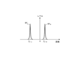
- FIG. 11 is a diagram showing the frequencies of received beat signals in a transmitting/receiving module in a master module system and a transmitting/receiving module in a slave module system.
- FIG. FIG. 11 is a block diagram showing a radar device according to a second embodiment.
- FIG. 11A and 11B are diagrams illustrating the influence of the frequency and DC component of a received beat signal in a transmitting/receiving module in a master module system and a transmitting/receiving module in a slave module system, respectively.
- FIG. 11 is a block diagram showing a radar device according to a third embodiment.
- Embodiment 1 A radar device according to a first embodiment will be described with reference to FIGS. 1 to 4.
- FIG. The radar device according to the first embodiment includes a master module system 100 and a plurality of slave module systems 200 1 to 200 n , and is a MIMO type FM-CW radar with a virtually enlarged antenna aperture.
- the number n of the slave module systems 200 1 to 200 n is the number required when a MIMO type FM-CW radar is mounted on a vehicle, and the number of modules is determined by a trade-off between performance and cost.
- the radar device further includes a trigger signal distribution circuit 30, trigger signal cables 40, 41 , 42.sub.1 to 42.sub.n , and reference signal cables 50.sub.1 to 50.sub.n.
- the trigger signal cables 40, 41, 42 1 to 42 n and the reference signal cables 50 1 to 50 n are coaxial cables.
- the master module system 100 and the plurality of slave module systems 200 1 to 200 n are mounted on a vehicle such as an automobile with the distance between the modules fixed. However, although the distance between the modules is fixed, the lengths of the trigger signal cables 40, 41, 42 1 to 42 n are not all necessarily the same, and the lengths of the reference signal cables 50 1 to 50 n are also not all necessarily the same.
- the master module system 100 and the multiple slave module systems 200 1 to 200 n share the trigger signal and the reference signal from the master module system 100 .
- the master module system 100 and the plurality of slave module systems 200 1 to 200 n share a trigger signal and a reference signal, so that the frequencies and operation timings of all the module systems are synchronized.
- the master module system 100 includes a transmitting/receiving module 10M, a transmitting antenna 10T, and a receiving antenna 10R.
- the plurality of slave module systems 200 1 to 200 n each include a transmission/reception module 20M 1 to 20M n , a transmission antenna 20T 1 to 20T n, and a reception antenna 20R 1 to 20R n . Since the multiple slave module systems 200 1 to 200 n each have the same configuration, except when it is necessary to distinguish between them, in the following explanation, one slave module system 200 will be described as a representative, and the subscripts will be omitted to avoid complexity.
- the transmitting/receiving module 10M in the master module system 100 includes a reference signal source 110, a transmitting/receiving circuit 120, a signal processing unit 130, and an ambient temperature monitor 140.
- the transmitting/receiving module 10M has a transmitting signal output terminal 10a, a receiving signal input terminal 10b, a trigger output terminal 10c, a trigger input terminal 10d, a reference signal output terminal 10e, and a target parameter output terminal 10g.
- the trigger input terminal 10d and the reference signal output terminal 10e are cable connectors.
- the transmitting/receiving module 20M in the slave module system 200 includes a transmitting/receiving circuit 220, a signal processing unit 230, and an ambient temperature monitor 240.
- the transmitting/receiving module 20M has a transmitting signal output terminal 20a, a receiving signal input terminal 20b, a trigger input terminal 20d, a reference signal input terminal 20f, a reference signal output terminal 20e, and a target parameter output terminal 20g.
- the trigger input terminal 20d, the reference signal input terminal 20f, and the reference signal output terminal 20e are cable connectors.
- the transmission/reception module 10M outputs a transmission RF signal from the transmission signal output terminal 10a to the transmission antenna 10T, receives a reception RF signal from the reception antenna 10R via the reception signal input terminal 10b, outputs a trigger signal (TRIG) from the trigger output terminal 10c to the trigger signal distribution circuit 30 via the trigger signal line 40, receives a trigger signal from the trigger signal distribution circuit 30 via the trigger signal cable 41 at the trigger input terminal 10d, and outputs a reference signal from the reference signal output terminal 10e to the transmission/reception module 20M in each of the multiple slave module systems 200.
- TMG trigger signal
- the trigger signal output from the trigger output terminal 10c is a pulse signal output at a period of, for example, 100 milliseconds.
- the trigger signal input from the trigger input terminal 10d is a reference signal that determines the start timing of a high-frequency chirp signal, which is a frequency-modulated signal whose frequency changes over time, and the sampling start timing of receiving AD conversion units (Analog to Digital Converters: ADCs) 125I and 125Q, which will be described later.
- AD conversion units Analog to Digital Converters: ADCs
- the reference signal is a signal that serves as a reference clock for generating a high-frequency chirp signal.
- the high-frequency chirp signal is a signal whose frequency changes linearly from 76 GHz to 77 GHz in 100 microseconds, that is, which up-chirps.
- the transmission/reception module 10M In response to a trigger signal input to the trigger input terminal 10d, the transmission/reception module 10M begins generating a high-frequency chirp signal based on the reference signal, that is, in synchronization with the reference signal, and outputs a transmission RF signal in which the high-frequency chirp signal is repeated to the transmission antenna 10T via the transmission signal output terminal 10a.
- the transmitting antenna 10T receives the transmission RF signal, converts it into a transmission wave in which FM-CW is repeated, and radiates the transmission wave into space.
- the receiving antenna 10R receives a reflected wave that is the transmission wave radiated by the transmitting antenna 10T and reflected by a target.
- the receiving antenna 10R converts the received reflected wave into a received RF signal in which a high-frequency chirp signal is repeated, and outputs the received RF signal to the transmitting/receiving module 10M via a received signal input terminal 10b.
- the transmission/reception module 10M processes the received RF signal input thereto to calculate the target's specifications (including distance, speed, and direction, hereinafter referred to as target specifications).
- the method of calculating the target specifications for the target by signal processing the received RF signal is carried out by a commonly known method.
- the target specifications are obtained by FFT (Fast Fourier Transform) processing a beat signal (IF signal) having a frequency which is the difference between the frequencies of the corresponding high frequency chirp signals of the transmitted RF signal (transmitted data) and the received RF signal (received data).
- FFT Fast Fourier Transform
- the transmission/reception module 10M separates the received RF signal into I/Q components, performs complex FFT processing using both the I and Q signals, and obtains a received beat signal obtained from the corresponding high-frequency chirp signal of the transmitted RF signal and the high-frequency chirp signal of the received RF signal.
- the obtained reception beat signal becomes a reference reception beat signal for the transmitting/receiving module 20M in the slave module system to obtain the timing offset amount. This function is performed before the radar device is shipped.
- the transmitting/receiving module 10M monitors the ambient temperature, and corrects the frequency of the received beat signal in accordance with the monitored ambient temperature.
- the transmission/reception module 10M outputs the calculated target specifications to an ECU (Electronic Control Unit) mounted on the vehicle.
- ECU Electronic Control Unit
- the transmission/reception module 10M includes a reference signal source 110, a transmission/reception circuit 120, a signal processing unit 130, and an ambient temperature monitor 140.
- the reference signal source 110 outputs a reference signal to the transmission/reception circuit 120 and also outputs a reference signal from a reference signal output terminal 10 e in order to provide the reference signal to the transmission/reception module 20 M in each of the plurality of slave module systems 200 .
- the reference signal from the reference signal source 110 is a signal that serves as a reference clock for the transmission/reception circuit 120 .
- the transmission/reception circuit 120 receives a trigger signal input to the trigger input terminal 10d and a reference signal from the reference signal source 110, and starts generating a high-frequency chirp signal based on the reference signal in response to the trigger signal.
- the transmission/reception circuit 120 outputs a transmission RF signal in which the high-frequency chirp signal is repeated to the transmission antenna 10T via the transmission signal output terminal 10a.
- the transmission/reception circuit 120 receives a received RF signal due to a reflected wave received by the receiving antenna 10R via the received signal input terminal 10b, generates a beat signal having a frequency which is the difference between the frequencies of the corresponding high-frequency chirp signals of the transmitted RF signal and the received RF signal, and outputs the I and Q signals of the I/Q separated beat signal to the signal processing unit 130.
- the transmission/reception circuit 120 includes an RF signal source 121, an amplifier 122, a complex-type quadrature mixer 123, high pass filters (HPFs) 124I and 124Q, and reception AD conversion units 125I and 125Q.
- the RF signal source 121 uses the reference signal as a reference clock and starts generating a high-frequency chirp signal, which is a transmission RF signal, in response to a trigger signal input from the trigger input terminal 10d.
- the amplifier 122 amplifies the transmission RF signal generated by the RF signal source 121 and outputs it to the transmission antenna 10T.
- Quadrature mixer 123 receives the transmission RF signal from RF signal source 121 and the reception RF signal from reception antenna 10R, and converts the reception RF signal into an I-axis reception beat signal and a Q-axis reception beat signal that are orthogonal to I/Q.
- the HPF 124I suppresses the low frequency components of the received beat signal on the I axis.
- the reception AD conversion section 125I uses the trigger signal input from the trigger input terminal 10d as the sampling start timing, and digitally converts the I-axis reception beat signal from the HPF 124I and outputs the digitalized signal to the signal processing section 130.
- the HPF 124Q suppresses the low frequency components of the received beat signal on the Q axis.
- the reception AD conversion section 125Q uses the trigger signal input from the trigger input terminal 10d as the sampling start timing, and digitally converts the Q-axis reception beat signal from the HPF 124Q and outputs the digitalized signal to the signal processing section 130.
- the signal processing unit 130 outputs a trigger signal from the trigger output terminal 10 c to the distribution circuit 30 .
- the signal processing unit 130 obtains the target parameters by performing FFT processing on the beat signal obtained by digitally converting a beat signal obtained from a high frequency chirp signal of a transmission RF signal that corresponds to the high frequency chirp signal of the reception RF signal generated by the orthogonal mixer 123.
- the calculation of the target parameters is performed by a generally known method.
- the target specifications may be corrected based on the ambient temperature monitored by the ambient temperature monitor 140 .
- the target specifications are outputted to the ECU from a target specification output terminal 10g.
- the signal processing unit 130 may obtain the target specifications by performing complex FFT processing on the I-axis reception beat signal from the reception AD conversion unit 125I and the Q-axis reception beat signal from the reception AD conversion unit 125Q.
- the signal processing unit 130 performs complex FFT processing on the I-axis beat signal from the reception AD conversion unit 125I and the Q-axis beat signal from the reception AD conversion unit 125Q, thereby obtaining a reception beat signal that serves as a reference for knowing the amount of timing deviation of the trigger signal in the slave module system.
- the signal processing unit 130 corrects the frequency of the received beat signal in accordance with the ambient temperature monitored by the ambient temperature monitor 140 . This function is performed before the radar device is shipped.
- the ambient temperature monitor 140 measures the ambient temperature of the transceiver module 10M, and outputs the measurement result to the signal processing unit 130.
- the signal processing unit 130 is made up of a processor 131, a memory 132, an input device 133, and an output device 134.
- the processor 131 is a central processing unit (CPU), a digital signal processor (DSP), or a field programmable gate array (FPGA).
- the memory 132 is a read only memory (ROM) and a random access memory (RAM).
- the I-axis reception beat signal from the reception AD conversion section 125I and the Q-axis reception beat signal from the reception AD conversion section 125Q are sent to the processor 131 via the input device 133.
- the processor 131 reads and executes a signal processing program (including complex FFT of received data (beat signal)) stored in the memory 132, thereby executing a process of calculating target specifications, a process of obtaining a received beat signal for obtaining the amount of timing offset, and a process of outputting the target specifications to the ECU via the output device 134.
- the processor 131 also executes a process of outputting a trigger signal to the trigger signal distribution circuit 30 via the output device 134 .
- the signal processing programs stored in the ROM of the memory 132 include a program for calculating target specifications, a program for obtaining a received beat signal, a program for outputting the target specifications, and a program for generating and outputting a trigger signal.
- the processor 131 temporarily reads out the program stored in the ROM into the RAM and executes it.
- the transmission/reception module 20M in the slave module system 200 outputs a transmission RF signal from the transmission signal output terminal 20a to the transmission antenna 20T, the reception RF signal from the reception antenna 20R is input via the reception signal input terminal 20b, the trigger signal from the trigger signal distribution circuit 30 is input via the trigger signal cable 42 to the trigger input terminal 20d, and the reference signal from the transmission/reception module 10M in the master module system 100 is input via the reference signal input terminal 20f.
- the reference signal input terminal 20f1 of the transmitting/receiving module 20M1 in the slave module system 2001 is connected to the reference signal output terminal 10e of the transmitting/receiving module 10M in the master module system 100 via a reference signal cable 501 .
- the reference signal input terminals 20f 2 to 20f n of the transmitting/receiving modules 20M 2 to 20M n are respectively connected to the reference signal output terminals 20e 1 to 20e n-1 of the transmitting/receiving modules 20M 1 to 20M n-1 having the next smaller number via reference signal cables 50 2 to 50 n .
- the reference signal cables 50 1 to 50 n are connection cables each having a pair of connectors.
- a reference signal from the transmitting/receiving module 10M in the master module system 100 is transmitted in sequence to the transmitting/receiving modules 20M 1 to 20M n in the multiple slave module systems 200 1 to 200 n .
- the transmitting/receiving module 10M in the master module system 100 and the transmitting/receiving modules 20M 1 to 20M n in the plurality of slave module systems 200 1 to 200 n operate based on a common reference signal.
- the reference signal Since the purpose of the reference signal is to synchronize the frequencies of the transmitting/receiving module 10M in the master module system 100 and the transmitting/receiving modules 20M 1 to 20M n in the multiple slave module systems 200 1 to 200 n , the frequency of the reference signal does not change when transmitted, so the operation of the transmitting/receiving modules 20M 1 to 20M n is not affected by delays caused by the reference signal cables 50 1 to 50 n and the transmission lines inside the transmitting/receiving modules 20M 1 to 20M n .
- the transmitting/receiving module 20M has the same configuration as the transmitting/receiving module 10M in the master module system 100, and operates in the same manner. That is, the transmission/reception module 20M begins generating a high-frequency chirp signal in synchronization with the reference signal input to the reference signal input terminal 20 in response to a trigger signal input to the trigger input terminal 20d, and outputs a transmission RF signal in which the high-frequency chirp signal is repeated to the transmission antenna 20T via the transmission signal output terminal 20a.
- the transmission/reception module 20M processes the received RF signal from the receiving antenna 20R, which is input via the received signal input terminal 20b, to calculate target specifications for the target.
- the transmission/reception module 20M separates the received RF signal into I/Q components, performs complex FFT processing using both the I and Q signals, and obtains a received beat signal obtained from the corresponding high-frequency chirp signal of the transmitted RF signal and the high-frequency chirp signal of the received RF signal.
- the transmitting/receiving module 20M obtains the amount of timing deviation in the trigger signal from the beat frequency in the obtained received beat signal, and stores the amount of timing deviation.
- the amount of timing offset is stored as a function of the monitored ambient temperature. This function is performed before the radar device is shipped.
- the timing offset in the trigger signal is obtained from the frequency difference between the beat frequency of the received beat signal obtained in the transmitting/receiving module 20M and the beat frequency of the received beat signal obtained in the transmitting/receiving module 10M of the master module system 100 obtained at the same timing. Since the received beat signal is obtained by performing complex FFT processing using both the I signal and the Q signal, the beat frequency in the received beat signal that exists at a negative distance is not aliased around the distance 0 (DC), and therefore the timing deviation amount can be obtained accurately.
- the transmission/reception module 20M When the radar device is in operation, that is, when the target specifications are obtained, the transmission/reception module 20M reads out the stored timing deviation amount, corrects the calculated target specifications according to the timing deviation amount, and outputs the corrected target specifications to the ECU.
- the transmission/reception module 20M corrects the values of the target specifications calculated so that the frequency difference of the beat frequencies indicated by the timing offset becomes zero, and outputs the corrected target specifications to the ECU.
- the target parameter is a distance
- the calculated distance value is corrected so that the frequency difference of the beat frequencies becomes zero, and the corrected distance information is output to the ECU.
- the transmission/reception module 20M monitors the ambient temperature, and reads out the stored timing offset amount according to the monitored ambient temperature.
- the transmitting/receiving module 20M includes a transmitting/receiving circuit 220, a signal processing unit 230, and an ambient temperature monitor 240.
- the transmitter/receiver circuit 220, signal processor 230, and ambient temperature monitor 240 are basically configured similarly to the transmitter/receiver circuit 120, signal processor 130, and ambient temperature monitor 140 in the transmitter/receiver module 10M in the master module system 100, and operate in the same manner.
- the transmission/reception circuit 220 includes an RF signal source 221, an amplifier 222, a complex quadrature mixer 223, HPFs 224I, 224Q, and reception AD conversion units 225I, 225Q, and outputs a transmission RF signal in which a high-frequency chirp signal is repeated to the transmission antenna 20T via the transmission signal output terminal 20a, generates a reception beat signal from the reception RF signal from the reception antenna 20R and the transmission RF signal, I/Q separates the reception beat signal, digitally converts it, and outputs the I signal and Q signal to the signal processing unit 130.
- the signal processing unit 230 is incorporated together with the signal processing unit 130 in the master module system 100 in a hardware configuration including a processor 131, a memory 132, an input device 133, and an output device 134. Note that the signal processing units 230 and the signal processing unit 130 may each be a separate hardware configuration.
- the signal processing unit 230 obtains target specifications by performing FFT processing on the digitally converted beat signal from the transmission/reception circuit 220 .
- the signal processing unit 230 obtains the received beat signal from the transmission/reception circuit 220 that has been I/Q separated and digitally converted.
- the signal processing unit 230 obtains the amount of timing offset in the trigger signal from the frequency difference between the beat frequency in the received beat signal obtained by the signal processing unit 130 in the transmitting/receiving module 10M of the master module system 100, which is obtained at the same timing as the beat frequency in the received beat signal, and stores the amount of timing offset in the memory 132.
- the signal processing unit 230 stores in the memory 132 the timing offset amount associated with the ambient temperature in accordance with the ambient temperature monitored by the ambient temperature monitor 240 . This function is performed before the radar device is shipped.
- the signal processing unit 230 reads from the memory 132 the timing offset of the trigger signal corresponding to the ambient temperature measured by the ambient temperature monitor 240, corrects the calculated target specifications so that the frequency difference of the beat frequency indicated by the read timing offset becomes zero, and outputs the corrected target specifications to the ECU from the target specifications output terminal 20g.
- the trigger signal distribution circuit 30 distributes a trigger signal from the transmitting/receiving module 10M of the master module system 100 and outputs the distributed trigger signal to the transmitting/receiving module 10M of the master module system 100 and each of the transmitting/receiving modules 20M 1 to 20M n of the multiple slave module systems 200 1 to 200 n via different trigger signal cables 41 , 42 1 to 42 n .
- the transmitting/receiving module 10M of the master module system 100 and the plurality of slave module systems 200 1 to 200 n receive the trigger signal distributed by the trigger signal distribution circuit 30 and therefore operate according to a common trigger signal.
- the trigger signal distribution circuit 30 has a trigger input terminal 30a to which a trigger signal is input from the trigger output terminal 10c in the transmitting/receiving module 10M of the master module system 100, a trigger output terminal 31 which outputs the trigger signal distributed to the trigger input terminal 10d in the transmitting/receiving module 10M of the master module system 100, and trigger output terminals 32 1 to 32 n which output the trigger signal distributed to each of the trigger input terminals 20d 1 to 20d n in the transmitting/receiving modules 20M 1 to 20M n of the multiple slave module systems 200 1 to 200 n .
- the trigger output terminal 31 and the trigger output terminals 32 1 to 32 n are cable connectors.
- the trigger signal cable 41 connecting the trigger output terminal 31 of the trigger signal distribution circuit 30 and the trigger input terminal 10d of the transmission/reception module 10M, and the trigger signal cables 42 1 to 42 n connecting each of the trigger output terminals 32 1 to 32 n of the trigger signal distribution circuit 30 and each of the trigger input terminals 20d 1 to 20d n in the transmission/reception modules 20M 1 to 20M n are each connection cables of approximately the same length and have a pair of connectors.
- the reference signal output from the reference signal source 110 of the transmitting/receiving module 10M in the master module system 100 is supplied to the transmitting/receiving circuit 120 and also supplied via reference signal cables 50 1 to 50 n to the transmitting/receiving circuits 220 1 to 220 n of the transmitting/receiving modules 20M 1 to 20M n in the multiple slave module systems 200 1 to 200 n , and is used as a reference clock.
- high-frequency chirp signals are generated based on a common reference clock generated by a reference signal, so that the high-frequency chirp signals generated by the transceiver circuit 120 and the transceiver circuits 220 1 to 220 n are synchronized in frequency.
- the trigger signal output from the signal processing unit 130 of the transmitting/receiving module 10M in the master module system 100 is a periodic pulse signal.
- the trigger signal output from the signal processing unit 130 is distributed by a trigger signal distribution circuit 30 and supplied to the transmitting/receiving module 10M in the master module system 100 and all of the transmitting/receiving modules 20M 1 to 20M n in the multiple slave module systems 200 1 to 200 n via a trigger signal cable 41 and trigger signal cables 42 1 to 42 n .
- the trigger signal distributed by the trigger signal distribution circuit 30 serves as a reference for the chirp start timing of the RF signal source 121 in the transceiver circuit 120 of the transceiver module 10M and the RF signal sources 221 1 to 221 in the transceiver circuits 220 1 to 220 n of the multiple slave module systems 200 1 to 200 n , and for the sample start timing of the reception AD conversion unit 125I and reception AD conversion unit 125Q in the transceiver circuit 120 and the reception AD conversion units 225I and reception AD conversion units 225Q in the transceiver circuits 220 1 to 220 n .
- the RF signal source 121 in the transmission/reception circuit 120 and the RF signal sources 221 1 to 221 in the transmission/reception circuits 220 1 to 220 n start generating high-frequency chirp signals.
- RF signal source 121 in transmission/reception circuit 120 and RF signal sources 221 1 to 221 in transmission/reception circuits 220 1 to 220 n each generate a high-frequency chirp signal based on a reference signal for frequency synchronization, and send a transmission RF signal to amplifier 122 and amplifiers 222 1 to 222 n , respectively.
- the amplifier 122 and each of the amplifiers 222 1 to 222 n amplify the high frequency chirp signal and send it to the transmitting antenna 10T and each of the transmitting antennas 20T 1 to 20T n .
- the transmitting antenna 10T and each of the transmitting antennas 20T 1 to 20T n radiate a high-frequency chirp signal as a transmission wave into space, and the receiving antenna 10R and each of the receiving antennas 20R 1 to 20R n receive the reflected wave from a target.
- the receiving antenna 10R and the receiving antennas 20R 1 to 20R n convert the reflected waves into received RF signals and send them to the quadrature mixer 123 and the quadrature mixers 223 1 to 223 n , respectively.
- the received RF signal is converted into an I signal beat signal (IF signal) and a Q signal beat signal (IF signal) that have been I/Q separated by the RF signal source 121 and the transmission RF signals from the RF signal sources 221 1 to 221 n , respectively.
- IF signal I signal beat signal
- IF signal Q signal beat signal
- the baseband signals of the I signal beat signal and the Q signal beat signal from the quadrature mixer 123 and the quadrature mixers 223 1 to 223 n , respectively, have unnecessary low-frequency components suppressed by the HPF 124I and the HPF 124Q, as well as the HPFs 224I 1 to 224I n and the HPFs 224Q 1 to 224Q n , respectively, and are converted into digital signals by the reception AD conversion unit 125I and the reception AD conversion unit 125Q, as well as the reception AD conversion units 225I 1 to 225I n and the reception AD conversion units 225Q 1 to 225Q n, respectively, and are sent to the signal processing unit 130 and the signal processing units 230 1 to 230 n , respectively.
- the signal processing unit 130 and each of the signal processing units 230 1 to 230 n calculate target specifications by performing FFT processing on beat signals (IF signals) generated by the received RF signals and the transmitted RF signals.
- IF signals beat signals
- the lengths of the trigger signal cable 41 and the trigger signal cables 42 1 to 42 n that supply the trigger signal to the transmission and reception module 10M and the transmission and reception modules 20M 1 to 20M n
- a difference will occur in the propagation time of the trigger signal from the trigger signal distribution circuit 30 depending on the lengths of the trigger signal cable 41 and the trigger signal cables 42 1 to 42 n for each of the transmission and reception module 10M and the transmission and reception modules 20M 1 to 20M n
- the chirp start timing will differ between the transmission and reception module 10M and the transmission and reception modules 20M 1 to 20M n .
- the frequency and phase of the received beat signal change according to the amount of timing deviation, resulting in an error in
- the signal processing units 230 1 to 230 n each reads out from the memory 132 the timing offset amount of the trigger signal obtained from the beat frequency of the received beat signal obtained by performing complex FFT processing on the I-axis beat signal (IF signal) converted into a digital signal from the reception AD conversion units 225I 1 to 225I n respectively and the Q-axis beat signal (IF signal) converted into a digital signal from the reception AD conversion units 225Q 1 to 225Q n respectively, and corrects the target specifications calculated by each of the signal processing units 230 1 to 230 n according to the read timing offset amount.
- IF signal I-axis beat signal
- IF signal Q-axis beat signal
- the signal processing unit 130 and each of the signal processing units 230 1 to 230 n obtain I/Q separated received beat signals, and each of the signal processing units 230 1 to 230 n corrects the target specifications using the timing deviation amount of the trigger signal obtained from the frequency difference between the beat frequency of the received beat signal of the signal processing unit 130 at the same timing as the beat frequency of its own received beat signal. Therefore, it is possible to correct errors in the target specifications caused by changes in the frequency and phase of the received beat signal due to variations in the lengths of the trigger signal cable 41 and the trigger signal cables 42 1 to 42 n , and suppress deterioration of detection accuracy.
- the timing offset of the trigger signal used in each of the signal processing units 230 1 to 230 n is detected before the shipment of the radar device, and the detected timing offset is stored in the memory of each of the signal processing units 230 1 to 230 n as a calibration table.
- the timing offset is read out from the calibration table stored in the memory to correct the target specifications.
- a target Tg or a target simulator is prepared, which is disposed at an equal distance from the receiving antenna 10R of the master module system 100 and the receiving antennas 20R 1 to 20R n of the slave module systems 200 1 to 200 n .
- a transmission wave is emitted from the transmitting antenna 10T of the master module system 100 toward the target Tg, and a reflected wave of the transmission wave from the target Tg is received by the receiving antenna 10R of the master module system 100 and the receiving antennas 20R 1 to 20R n of the slave module systems 200 1 to 200 n .
- no transmission waves are radiated from the transmission antennas 20T 1 to 20T n of the slave module systems 200 1 to 200 n .
- the signal processing unit 130 of the transmitting/receiving module 10M in the master module system 100 and the signal processing units 230 1 to 230 n of the transmitting/receiving modules 20M 1 to 20M n in the slave module systems 200 1 to 200 n each obtain an I/Q separated received beat signal.
- Each of the signal processing units 230 1 to 230 n stores in the memory 132 a frequency difference between the beat frequency of its own I/Q separated received beat signal and the beat frequency of the I/Q separated received beat signal of the signal processing unit 130 obtained at the same timing as the beat frequency of the I/Q separated received beat signal of the signal processing unit 130, as a timing shift amount of the trigger signal, in association with the ambient temperature monitored by the ambient temperature monitor 240.
- the chirp signal start timing of the RF signal source 221 in the slave module system 200 lags behind the chirp signal start timing of the RF signal source 121 in the master module system 100 by a time ⁇ error
- the transmit RF signal TR S from the RF signal source 221 lags behind the transmit RF signal TR M from the RF signal source 121 by a time ⁇ error , as shown in FIG. 3.
- the received RF signal RE M input to the quadrature mixer 123 in the master module system 100 lags behind the transmitted RF signal TR M by a time ⁇ 1 as shown in FIG.
- the received RF signal RES input to the quadrature mixer 223 in the slave module system 200 has the same timing as the received RF signal REM , and is delayed by a time ⁇ 1 from the transmitted RF signal TRM .
- FIG. 3 shows the chirp waveforms of the master module system 100 and the slave module system 200.
- the horizontal axis represents time and the vertical axis represents frequency, with TR M representing the transmitted RF signal of the transmitting/receiving module 10M in the master module system 100, RE M representing the received RF signal of the transmitting/receiving module 10M in the master module system 100, TR S representing the transmitted RF signal of the transmitting/receiving module 10M in the slave module system 200, and RES representing the received RF signal of the transmitting/receiving module 10M in the slave module system 200.
- FIG. 4 shows the beat frequency f if_M of the received beat signal BF M obtained by performing complex FFT processing by the signal processing unit 130 using the beat signal based on the received RF signal RE M and the transmitted RF signal TR M, and the beat frequency f if_S of the received beat signal BF S obtained by performing complex FFT processing by the signal processing unit 230 using the beat signal based on the received RF signal RES and the transmitted RF signal TR S.
- the horizontal axis indicates distance (beat frequency) and the vertical axis indicates level, with BFM indicating the received beat signal calculated by signal processing unit 130 and BFS indicating the received beat signal calculated by signal processing unit 230.
- the orthogonal mixer 223 performs I/Q separation of the beat signals (IF signals) due to the input received RF signal RES and transmitted RF signal TR S , and the signal processing unit 230 performs complex FFT processing using both the I signal and the Q signal. Therefore, even if the received beat signal BF S exists in the negative frequency domain, aliasing does not occur, and the received beat signal BF S exhibits a correct value as shown in FIG. 4.
- the beat frequency f if_M of the received beat signal BF M obtained by the signal processing unit 130 can be expressed by the following equation (1)
- the beat frequency f if_S of the received beat signal BF S obtained by the signal processing unit 230 can be expressed by the following equation (2).
- f if_M (B/T c ) ⁇ 1 ...(1)
- f if_S (B/T c ) ( ⁇ 1 - ⁇ error ) ...
- the timing shift amount f if_(S -M) of the trigger signal in the slave module system 200 relative to the master module system 100 corresponds to the frequency difference between the beat frequency f if_M of the received beat signal BF M and the beat frequency f if_S of the received beat signal BF S , and can be expressed by the following equation (3).
- f if_(S -M) f if_S - f if_M ...(3)
- Even if the time ⁇ error is greater than the time ⁇ 1 , the beat frequency f if_S of the received beat signal BF S indicates a correct value, and therefore the timing offset f if_(S ⁇ M) also indicates a correct value.
- the signal processing unit 130 stores the timing offset f if_(S ⁇ M) obtained by the above equation (3) in the memory 132 in association with the ambient temperature. Furthermore, while changing the ambient temperatures of the transmitting and receiving module 10M in the master module system 100 and the transmitting and receiving modules 20M 1 to 20M n in the plurality of slave module systems 200 1 to 200 n , the timing offset f if_(S -M) in each of the plurality of slave module systems 200 1 to 200 n is calculated. That is, by calculating the timing offset f if_(S -M) while changing the ambient temperature, it is possible to correct the temperature characteristic of the timing offset f if_(S -M) .
- a calibration table is created in the memory 132 that associates the ambient temperature monitored by each of the ambient temperature monitors 240 1 to 240 n with the timing offset amount f if_(S -M) calculated at the ambient temperature at the time of monitoring, and the calibration table for the signal processing units 230 1 to 230 n is stored in the memory 132.
- a calibration table that associates the ambient temperature monitored by the ambient temperature monitor 140 with the beat frequency f if_M of the received beat signal BF M calculated at the ambient temperature at the time of monitoring is created in the memory 132, and is stored in the memory 132 for the signal processing unit 130.
- a calibration table that associates the ambient temperature with the timing offset amount f if_(S -M) is stored in the memory 132 for the signal processing units 230 1 to 230 n.
- the signal processing units 230 1 to 230 n in each of the slave module systems 200 1 to 200 n read out the timing offset amount f if_(S -M) from the calibration table in accordance with the ambient temperature monitored by each of the ambient temperature monitors 240 1 to 240 n , and correct the target specifications using the read out timing offset amount f if_(S -M) .
- the trigger signal from the transmission/reception module 10M of the master module system 100 is distributed by the trigger signal distribution circuit 30 and provided to the transmission/reception module 10M of the master module system 100 and the transmission/reception modules 20M of the multiple slave module systems 200 via different trigger signal cables 41, 42, respectively, and the reference signal from the transmission/reception module 10M of the master module system 100 is output to the transmission/reception modules 20M of the multiple slave module systems 200, and in the transmission/reception modules 20M of the multiple slave module systems 200, a high-frequency chirp of the received RF signal due to the reflected wave received by the receiving antenna 20R is generated.
- the target parameters obtained by FFT processing the beat signal obtained from the high frequency chirp signal of the transmitted RF signal that corresponds to the signal are corrected by the timing offset amount obtained from the beat frequency of the received beat signal that has been I/Q separated using the received RF signal and complex FFT processed. Therefore, even if the lengths of the trigger signal cables 41, 42 are different and a timing offset occurs between the trigger signals, the correctly obtained timing offset amount can be used, and the timing offset can be correctly corrected for the transmission/reception module 20M of the slave module system 200 relative to the transmission/reception module 10M of the master module system 100, and the deterioration of radar performance can be suppressed.
- the radar device can store the timing offset amount in a calibration table in association with the ambient temperature, and can read out the timing offset amount from the calibration table according to the ambient temperature, thereby correcting the target specifications with higher accuracy.
- Embodiment 2 A radar device according to a second embodiment will be described with reference to FIGS.
- the radar device according to the second embodiment is different from the radar device according to the first embodiment in that delay circuits 250 1 to 250 n are further provided for the transmission/reception modules 20M 1 to 20M n of the slave module systems 200 1 to 200 n , but is otherwise similar.
- the delay circuits 250 1 to 250 n each have the same function and operation, they will be explained as a representative of the transmitting/receiving module 20M in one slave module system 200, and subscripts will be omitted to avoid complication.
- the same reference numerals as those in Figs. 1 to 4 designate the same or corresponding parts.
- the delay circuit 250 is connected between the trigger input terminal 20 d and the transmission/reception circuit 220 .
- the delay circuit 250 is a delay circuit that can vary the amount of delay.
- the trigger signal delayed by the delay circuit 250 determines the start timing of the high frequency chirp signal from the RF signal source 221 and the sampling start timing of the reception AD conversion units 225I and 225Q.
- the delay circuit 250 delays the trigger signal input to the trigger input terminal 20d by reducing the transmission leakage in the transmission RF signal from the RF signal source 221 and the reception antenna 20R.
- the trigger signal is delayed in order to avoid degradation of the signal-to-noise ratio (SNR) of the received beat signal due to the presence of a direct current (DC) component due to the influence of a DC offset in the receiving circuit, which is a path for processing the received RF signal from the quadrature mixer 223, the HPFs 224I and 224Q, and the receiving AD conversion units 225I and 225Q.
- SNR signal-to-noise ratio
- DC direct current
- the timing offset calculated by the signal processing unit 230 is offset, so that the frequency of the received beat signal can be obtained without being affected by the DC component, and the timing offset can be obtained with high accuracy.
- target specifications can be obtained with high accuracy, and degradation of detection accuracy can be suppressed.
- the delay amount in the delay circuit 250 is set before the radar device is shipped.
- a target Tg or a target simulator is prepared, which is placed at an equal distance from the receiving antenna 10R of the master module system 100 and the receiving antennas 20R 1 to 20R n of the slave module systems 200 1 to 200 n .
- a transmission wave is emitted from the transmitting antenna 10T of the master module system 100 toward the target Tg, and a reflected wave of the transmission wave from the target Tg is received by the receiving antenna 10R of the master module system 100 and the receiving antennas 20R 1 to 20R n of the slave module systems 200 1 to 200 n .
- no transmission waves are radiated from the transmission antennas 20T 1 to 20T n of the slave module systems 200 1 to 200 n .
- a DC component may exist within the frequency band of the received RF signal of the transmitting/receiving module 20M in the slave module system 200. That is, the beat frequency f if_S0 of the received beat signal BFS0 obtained by performing complex FFT processing on the transmit RF signal TR S and the receive RF signal RES when the trigger signal is not delayed by the delay circuit 250 by the signal processing unit 230 is in a region in which the DC component of the transmit/receive circuit 220 in the transmit/receive module 20M exists, as shown in FIG. 6 .
- the tri-phase signal is delayed by a delay circuit, and the beat frequency f if_S0 of the received beat signal BFS0 converted by performing complex FFT processing using the transmitted RF signal TR S and the received RF signal RES is offset to a region outside the beat frequency region in which a DC component exists, as shown in FIG .
- the horizontal axis represents distance (beat frequency), the vertical axis represents level, BF M represents the received beat signal calculated by the signal processing unit 130, BF S0 represents the received beat signal calculated by the signal processing unit 230 when the trigger signal is not delayed, BF S represents the received beat signal calculated by the signal processing unit 230 when the trigger signal is delayed, and DC represents the direct current component generated by the transmission and reception circuit 220 in the transmission and reception module 20M.
- the beat frequency f if_S of the received beat signal BF S obtained by the signal processing unit 230 can be expressed by the following equation (4).
- f if_S (B/T c ) ( ⁇ 1 - ⁇ error - ⁇ a )...(4)
- the beat frequency f if_M of the received beat signal BF M can be expressed by the above formula (1)
- the beat frequency f if_S0 of the received beat signal BF S0 can be expressed by the above formula (2).
- the delay time ⁇ a in the delay circuit is set by the signal processing unit 230 . That is, the signal processing unit 230 outputs a digital value indicating the amount of offset corresponding to the beat frequency f if_S of the received beat signal BF S to the delay circuit 250, and the delay circuit 250 varies the amount of delay in accordance with the digital value, thereby setting the delay time ⁇ a .
- a digital value indicating the amount of offset is stored in memory 132 for signal processing section 230 .
- the signal processing unit 230 has a delay time setting program stored in the memory 132 shown in FIG.
- the delay time setting program is a program which compares the beat frequency f if_S of the received beat signal BF S obtained by the signal processing unit 230 with a set beat frequency which is a threshold value set outside the region where the direct-current component DC exists, and if the beat frequency is equal to or lower than the set beat frequency, outputs a digital amount corresponding to the difference between the received beat signal BF S and the beat frequency which exceeds the set frequency to the delay circuit 250.
- the signal processing unit 230 obtains the timing offset f if_(S ⁇ M) before shipping the radar device, and stores it in the memory 132, in the same manner as described in the radar device according to the first embodiment. At this time, since the received beat signal BFS has a frequency that can avoid the influence of DC components that deteriorate the S/N ratio, the amount of timing deviation can be obtained with high accuracy.
- the signal processing unit 230 performs FFT processing on the beat signal converted from the received RF signal to calculate target specifications, reads out from the memory 132 the timing offset f if_(S -M) associated with the ambient temperature monitored by the ambient temperature monitor 240 and an offset amount (delay time), and corrects the calculated target specifications, taking into account the read offset amount, so that the timing offset f if_(S -M) becomes zero.
- the offset amount read out at this time is a value corresponding to the delay time ⁇ a by which the beat frequency f if_S of the received beat signal BFS is delayed in consideration of the influence of the direct current component DC, as shown in the above formula (4), and therefore a highly accurate beat frequency can be obtained.
- the influence of degradation in the S/N ratio can be avoided, the timing offset f if_(S -M) is highly accurate, and degradation of radar performance can be suppressed.
- the offset amount (delay time) and timing deviation amount of the trigger signal used in each of the signal processing units 230 1 to 230 n are determined before shipment of the radar device by determining the delay time ⁇ a , detecting the timing deviation amount, and storing the delay amount equivalent to the delay time ⁇ a and the detected timing deviation amount as a calibration table in the memory of each of the signal processing units 230 1 to 230 n .
- the radar device according to the second embodiment has the same effects as the radar device according to the first embodiment, and in addition, in the transceiver module 20M of each of the multiple slave module systems 200, the trigger signal that starts the generation of the high-frequency chirp signal is the trigger signal distributed from the trigger signal distribution circuit 30 via the delay circuit 250. Therefore, the beat frequency in the received beat signal obtained by I/Q separation of the received RF signal is always set outside the region in which the direct current component DC exists. This allows the use of a highly accurate timing offset amount, and the deterioration of radar performance can be further suppressed.
- Embodiment 3 A radar device according to the third embodiment will be described with reference to FIG.
- the radar device of embodiment 3 differs from the radar device of embodiment 2 in that, whereas the radar device of embodiment 2 uses a target Tg or a target simulator to determine the timing offset and the delay amount (delay time ⁇ a ) in the delay circuit 250, the radar device of embodiment 3 obtains the timing offset and the delay amount in the delay circuit 250 by directly receiving the transmission wave from the transmitting antenna 10T of the master module system 100 as a direct wave by the receiving antenna 10R of the master module system 100 and the receiving antennas 20R 1 to 20R n of the slave module systems 200 1 to 200 n , but is otherwise the same.
- the same reference numerals as those in FIG. 5 designate the same or corresponding parts.
- the setting of the timing offset amount and the setting of the delay time ⁇ a in the delay circuit 250 are performed when the ambient temperature monitored by the ambient temperature monitor 240 during operation of the radar device changes to a set value or more compared to the previous setting, and also periodically and cyclically.
- the delay time ⁇ a in the delay circuit 250 i.e., the offset amount and timing deviation amount
- the signal processing section 230 reads out the offset amount and timing deviation amount stored in the memory 132, and taking into account the calculated offset amount read from the target specifications, corrects the target specifications using the timing deviation amount, and outputs the corrected target specifications from the target specifications output terminal 20g to the ECU.
- the master module system 100 and the multiple slave module systems 200 1 to 200 n are fixed in position, the distance between the transmitting antenna 10T of the master module system 100 and each of the receiving antennas 20R 1 to 20R n of the multiple slave module systems 200 1 to 200 n is fixed, and the relationship between the received RF signal input to the transmitting/receiving module 10M of the master module system 100 and the received RF signal input to each of the transmitting/receiving modules 20M 1 to 20M n of the multiple slave module systems 200 1 to 200 n is uniquely determined.
- a transmission wave is radiated into space from the transmitting antenna 10T of the master module system 100, and the direct wave from the transmitting antenna 10T is directly received by the receiving antenna 10R of the master module system 100 and the receiving antennas 20R1 to 20Rn of the slave module systems 2001 to 200n.
- the timing offset of the trigger signal in each of the slave module systems 2001 to 200n relative to the master module system 100 can be obtained.
- no transmission waves are emitted from the transmission antennas 20T 1 to 20T n of the slave module systems 200 1 to 200 n .
- the beat frequency f if_M of the received beat signal BF M obtained by the signal processing unit 130 can be expressed by the above formula (1).
- ⁇ 1 is the time from when the transmit RF signal TR M is output until when the direct wave is received and the receive RF signal RE M is obtained.
- the beat frequency f if_S of the received beat signal BF S obtained by the signal processing unit 230 can be expressed by replacing the delay time ⁇ 1 with ⁇ 2 in the above equation (2).
- ⁇ 2 is the time from when the transmission RF signal TR M is output to when the direct wave is received to obtain the reception RF signal RES, which is ⁇ 1 + ⁇ , where ⁇ is the time based on the distance between the transmission antenna 10T and each of the reception antennas 20R1 to 20Rn .
- the timing offset f if_(S ⁇ M) can be calculated by the above equation (3).
- the timing offset f if_(S -M) thus obtained is stored in the storage section of the memory 132 corresponding to the signal processing section 230 and is maintained until the next setting.
- the timing offset amount f if_(S -M) stored in the memory 132 is saved in association with the ambient temperature monitored by the ambient temperature monitor 240 at the time of setting.
- the quadrature mixer 223 performs I/Q separation on the beat signals (IF signals) resulting from the input received RF signal RES and transmitted RF signal TR S , and the signal processing unit 230 performs complex FFT processing using both the I signal and the Q signal to obtain the received beat signal BF S. Therefore, a correct value is obtained for the received beat signal BF S , and the timing offset f if_(S -M) also indicates a correct value. As a result, when the target specifications are acquired, the target specifications are corrected using the timing offset f if_(S -M) that indicates the correct value, so that degradation of detection performance can be suppressed.
- the timing offset amount f if_(S -M) is automatically reset, so that it is possible to suppress deterioration of radar performance caused by a shift in the timing of the trigger signal based on the effect of the temperature characteristics of the trigger signal cable 42 caused by a change in ambient temperature. Furthermore, since the timing offset f if_(S -M) is automatically reset periodically or cyclically, it is possible to suppress degradation of radar performance caused by shifts in the timing of the trigger signal due to deterioration over time of the trigger signal cable 42 or the transmission/reception module 20M.
- the delay time ⁇ a is also set at the same timing as when the timing deviation amount is set.
- the direct wave from the transmitting antenna 10T is directly received by the receiving antenna 10R of the master module system 100 and the receiving antennas 20R 1 to 20R n of the slave module systems 200 1 to 200 n , and the delay time ⁇ a in the delay circuit 250 can be obtained by using each received RF signal.
- no transmission waves are emitted from the transmission antennas 20T 1 to 20T n of the slave module systems 200 1 to 200 n .
- the beat frequency f if_S of the received beat signal BF S obtained by the signal processing unit 230 can be expressed by replacing the delay time ⁇ 1 with ⁇ 2 in the above equation (4), in the same manner as described in the second embodiment, with respect to the amount of timing deviation.
- the delay time ⁇ a corresponding to the offset amount is a value by which the beat frequency f if_S of the received beat signal BF S obtained by performing complex FFT processing using the transmitted RF signal TR S and the received RF signal RES is offset to a value outside the region of beat frequencies in which a DC component exists.
- the signal processing unit 230 outputs a digital value indicating the amount of offset corresponding to the beat frequency f if_S of the received beat signal BF S to the delay circuit 250, and the delay circuit 250 varies the amount of delay in accordance with the digital value, thereby setting the delay time ⁇ a .
- the digital value indicating the offset amount thus obtained is stored in the storage section of the memory 132 corresponding to the signal processing section 230 and is maintained until the next setting. At this time, since the received beat signal BFS has a frequency that can avoid the influence of DC components that deteriorate the S/N ratio, the amount of timing deviation can be obtained with high accuracy.
- the signal processing unit 230 When acquiring the target specifications, the signal processing unit 230 reads the offset amount and timing deviation amount stored in the memory 132, corrects the calculated target specifications using the read timing deviation amount while taking into account the read offset amount, and outputs the corrected target specifications to the ECU from the target specification output terminal 20g.
- the radar device according to the third embodiment has the same effects as the radar device according to the first embodiment or the radar device according to the second embodiment.
- the timing offset amount and the delay time ⁇ a in the delay circuit 250 are set during operation of the radar device, the timing offset amount can be appropriately set in response to changes in the ambient temperature, changes in the condition of the trigger signal cable 42 over time, and the like.
- the radar device disclosed herein is suitable for use as a radar device mounted on an automobile to detect targets.
Landscapes
- Engineering & Computer Science (AREA)
- Radar, Positioning & Navigation (AREA)
- Remote Sensing (AREA)
- Computer Networks & Wireless Communication (AREA)
- Physics & Mathematics (AREA)
- General Physics & Mathematics (AREA)
- Radar Systems Or Details Thereof (AREA)
Priority Applications (2)
| Application Number | Priority Date | Filing Date | Title |
|---|---|---|---|
| PCT/JP2023/022519 WO2024261792A1 (ja) | 2023-06-19 | 2023-06-19 | レーダ装置 |
| JP2024563201A JPWO2024261792A1 (https=) | 2023-06-19 | 2023-06-19 |
Applications Claiming Priority (1)
| Application Number | Priority Date | Filing Date | Title |
|---|---|---|---|
| PCT/JP2023/022519 WO2024261792A1 (ja) | 2023-06-19 | 2023-06-19 | レーダ装置 |
Publications (1)
| Publication Number | Publication Date |
|---|---|
| WO2024261792A1 true WO2024261792A1 (ja) | 2024-12-26 |
Family
ID=93935078
Family Applications (1)
| Application Number | Title | Priority Date | Filing Date |
|---|---|---|---|
| PCT/JP2023/022519 Ceased WO2024261792A1 (ja) | 2023-06-19 | 2023-06-19 | レーダ装置 |
Country Status (2)
| Country | Link |
|---|---|
| JP (1) | JPWO2024261792A1 (https=) |
| WO (1) | WO2024261792A1 (https=) |
Citations (6)
| Publication number | Priority date | Publication date | Assignee | Title |
|---|---|---|---|---|
| US20180372865A1 (en) * | 2017-06-23 | 2018-12-27 | Nxp B.V. | Automotive radar system and method of synchronising an automotive radar system |
| JP2018205218A (ja) * | 2017-06-07 | 2018-12-27 | 三菱電機株式会社 | レーダ装置 |
| US20200003883A1 (en) * | 2018-07-02 | 2020-01-02 | Nxp Usa, Inc. | Communication unit, integrated circuits and method for clock and data synchronization |
| JP2020513539A (ja) * | 2016-10-26 | 2020-05-14 | 日本テキサス・インスツルメンツ合同会社 | Icチップに対するタイミング |
| JP2021025834A (ja) * | 2019-08-01 | 2021-02-22 | 三菱電機株式会社 | レーダ装置 |
| JP2022045714A (ja) * | 2020-09-09 | 2022-03-22 | 三菱電機株式会社 | レーダ装置 |
Family Cites Families (1)
| Publication number | Priority date | Publication date | Assignee | Title |
|---|---|---|---|---|
| JP2795866B2 (ja) * | 1989-01-20 | 1998-09-10 | 株式会社東芝 | アレイアンテナ装置 |
-
2023
- 2023-06-19 JP JP2024563201A patent/JPWO2024261792A1/ja active Pending
- 2023-06-19 WO PCT/JP2023/022519 patent/WO2024261792A1/ja not_active Ceased
Patent Citations (6)
| Publication number | Priority date | Publication date | Assignee | Title |
|---|---|---|---|---|
| JP2020513539A (ja) * | 2016-10-26 | 2020-05-14 | 日本テキサス・インスツルメンツ合同会社 | Icチップに対するタイミング |
| JP2018205218A (ja) * | 2017-06-07 | 2018-12-27 | 三菱電機株式会社 | レーダ装置 |
| US20180372865A1 (en) * | 2017-06-23 | 2018-12-27 | Nxp B.V. | Automotive radar system and method of synchronising an automotive radar system |
| US20200003883A1 (en) * | 2018-07-02 | 2020-01-02 | Nxp Usa, Inc. | Communication unit, integrated circuits and method for clock and data synchronization |
| JP2021025834A (ja) * | 2019-08-01 | 2021-02-22 | 三菱電機株式会社 | レーダ装置 |
| JP2022045714A (ja) * | 2020-09-09 | 2022-03-22 | 三菱電機株式会社 | レーダ装置 |
Also Published As
| Publication number | Publication date |
|---|---|
| JPWO2024261792A1 (https=) | 2024-12-26 |
Similar Documents
| Publication | Publication Date | Title |
|---|---|---|
| US20200150255A1 (en) | Calibration of a multifunctional automotive radar system | |
| KR20180113502A (ko) | 레이더 시스템에서 위상 잡음에 의해 초래되는 간섭을 감소시키기 위한 방법 및 시스템 | |
| US11675047B2 (en) | System and method for local oscillator drift estimation and compensation in cascaded sensors | |
| KR102495488B1 (ko) | 동기화된 고주파 모듈을 갖는 fmcw 레이더 센서 | |
| US10175352B2 (en) | Scalable architecture for an automotive radar system | |
| US10505770B2 (en) | Reception signal processing device, radar, and object detection method | |
| JP6295011B2 (ja) | 送信器、送信方法、位相調整装置、位相調整方法 | |
| JP6701124B2 (ja) | レーダ装置 | |
| Lutz et al. | Target simulator concept for chirp modulated 77 GHz automotive radar sensors | |
| JP6324327B2 (ja) | パッシブレーダ装置 | |
| US20240310474A1 (en) | Cascaded radar system with transmiting-vehicle reflection mitigation | |
| JP6130195B2 (ja) | レーダシステム | |
| KR20210109855A (ko) | 차량용 레이더의 송신신호 위상 보정 장치 및 방법과, 그를 포함하는 차량용 레이더 장치 | |
| JP7704301B2 (ja) | 測位システムおよびそれを備える車両、並びに測位方法 | |
| CN112119328A (zh) | 雷达装置 | |
| WO2024261792A1 (ja) | レーダ装置 | |
| KR101324172B1 (ko) | 다채널 디지털 수신장치의 신호도착시간(toa) 보정방법 및 장치 | |
| JP2022045714A (ja) | レーダ装置 | |
| US11428776B2 (en) | System for measuring phase coherence as well as method of measuring phase coherence | |
| KR20260023536A (ko) | 물리적으로 분산된 어셈블리에 대한 코히어런트 결합을 가능하게 하는 동기화 방법 및 시스템 | |
| WO2022081616A1 (en) | Synchronized power and/or temperature measurement in a millimeter wave (mmw) front end module | |
| US12366652B2 (en) | Apparatus and method for controlling radar in vehicle | |
| JP2024177901A (ja) | レーダ装置 | |
| JP5707679B2 (ja) | 受信装置及びその方法並びにレーダ装置及びその受信方法 | |
| JP7111455B2 (ja) | レーダ装置およびレーダ装置の制御方法 |
Legal Events
| Date | Code | Title | Description |
|---|---|---|---|
| WWE | Wipo information: entry into national phase |
Ref document number: 2024563201 Country of ref document: JP |
|
| 121 | Ep: the epo has been informed by wipo that ep was designated in this application |
Ref document number: 23942231 Country of ref document: EP Kind code of ref document: A1 |
|
| NENP | Non-entry into the national phase |
Ref country code: DE |