WO2024257619A1 - 発光素子の製造方法及び発光素子 - Google Patents
発光素子の製造方法及び発光素子 Download PDFInfo
- Publication number
- WO2024257619A1 WO2024257619A1 PCT/JP2024/019848 JP2024019848W WO2024257619A1 WO 2024257619 A1 WO2024257619 A1 WO 2024257619A1 JP 2024019848 W JP2024019848 W JP 2024019848W WO 2024257619 A1 WO2024257619 A1 WO 2024257619A1
- Authority
- WO
- WIPO (PCT)
- Prior art keywords
- light
- insulating film
- electrode
- semiconductor layer
- emitting element
- Prior art date
- Legal status (The legal status is an assumption and is not a legal conclusion. Google has not performed a legal analysis and makes no representation as to the accuracy of the status listed.)
- Ceased
Links
Images













Classifications
-
- H—ELECTRICITY
- H10—SEMICONDUCTOR DEVICES; ELECTRIC SOLID-STATE DEVICES NOT OTHERWISE PROVIDED FOR
- H10H—INORGANIC LIGHT-EMITTING SEMICONDUCTOR DEVICES HAVING POTENTIAL BARRIERS
- H10H20/00—Individual inorganic light-emitting semiconductor devices having potential barriers, e.g. light-emitting diodes [LED]
- H10H20/80—Constructional details
- H10H20/83—Electrodes
- H10H20/831—Electrodes characterised by their shape
- H10H20/8314—Electrodes characterised by their shape extending at least partially onto an outer side surface of the bodies
-
- H—ELECTRICITY
- H10—SEMICONDUCTOR DEVICES; ELECTRIC SOLID-STATE DEVICES NOT OTHERWISE PROVIDED FOR
- H10H—INORGANIC LIGHT-EMITTING SEMICONDUCTOR DEVICES HAVING POTENTIAL BARRIERS
- H10H20/00—Individual inorganic light-emitting semiconductor devices having potential barriers, e.g. light-emitting diodes [LED]
- H10H20/01—Manufacture or treatment
- H10H20/032—Manufacture or treatment of electrodes
-
- H—ELECTRICITY
- H10—SEMICONDUCTOR DEVICES; ELECTRIC SOLID-STATE DEVICES NOT OTHERWISE PROVIDED FOR
- H10H—INORGANIC LIGHT-EMITTING SEMICONDUCTOR DEVICES HAVING POTENTIAL BARRIERS
- H10H20/00—Individual inorganic light-emitting semiconductor devices having potential barriers, e.g. light-emitting diodes [LED]
- H10H20/80—Constructional details
- H10H20/83—Electrodes
- H10H20/831—Electrodes characterised by their shape
-
- H—ELECTRICITY
- H10—SEMICONDUCTOR DEVICES; ELECTRIC SOLID-STATE DEVICES NOT OTHERWISE PROVIDED FOR
- H10H—INORGANIC LIGHT-EMITTING SEMICONDUCTOR DEVICES HAVING POTENTIAL BARRIERS
- H10H20/00—Individual inorganic light-emitting semiconductor devices having potential barriers, e.g. light-emitting diodes [LED]
- H10H20/01—Manufacture or treatment
- H10H20/036—Manufacture or treatment of packages
- H10H20/0363—Manufacture or treatment of packages of optical field-shaping means
-
- H—ELECTRICITY
- H10—SEMICONDUCTOR DEVICES; ELECTRIC SOLID-STATE DEVICES NOT OTHERWISE PROVIDED FOR
- H10H—INORGANIC LIGHT-EMITTING SEMICONDUCTOR DEVICES HAVING POTENTIAL BARRIERS
- H10H20/00—Individual inorganic light-emitting semiconductor devices having potential barriers, e.g. light-emitting diodes [LED]
- H10H20/80—Constructional details
- H10H20/81—Bodies
- H10H20/819—Bodies characterised by their shape, e.g. curved or truncated substrates
- H10H20/82—Roughened surfaces, e.g. at the interface between epitaxial layers
-
- H—ELECTRICITY
- H10—SEMICONDUCTOR DEVICES; ELECTRIC SOLID-STATE DEVICES NOT OTHERWISE PROVIDED FOR
- H10H—INORGANIC LIGHT-EMITTING SEMICONDUCTOR DEVICES HAVING POTENTIAL BARRIERS
- H10H20/00—Individual inorganic light-emitting semiconductor devices having potential barriers, e.g. light-emitting diodes [LED]
- H10H20/80—Constructional details
- H10H20/83—Electrodes
- H10H20/832—Electrodes characterised by their material
- H10H20/833—Transparent materials
-
- H—ELECTRICITY
- H10—SEMICONDUCTOR DEVICES; ELECTRIC SOLID-STATE DEVICES NOT OTHERWISE PROVIDED FOR
- H10H—INORGANIC LIGHT-EMITTING SEMICONDUCTOR DEVICES HAVING POTENTIAL BARRIERS
- H10H20/00—Individual inorganic light-emitting semiconductor devices having potential barriers, e.g. light-emitting diodes [LED]
- H10H20/80—Constructional details
- H10H20/85—Packages
- H10H20/8502—Surface mount technology [SMT] type packages
-
- H—ELECTRICITY
- H10—SEMICONDUCTOR DEVICES; ELECTRIC SOLID-STATE DEVICES NOT OTHERWISE PROVIDED FOR
- H10H—INORGANIC LIGHT-EMITTING SEMICONDUCTOR DEVICES HAVING POTENTIAL BARRIERS
- H10H20/00—Individual inorganic light-emitting semiconductor devices having potential barriers, e.g. light-emitting diodes [LED]
- H10H20/80—Constructional details
- H10H20/85—Packages
- H10H20/855—Optical field-shaping means, e.g. lenses
- H10H20/856—Reflecting means
Definitions
- the present invention relates to a method for manufacturing a light-emitting element and a light-emitting element.
- Patent Document 1 discloses a light-emitting element having a first electrode arranged on the main light extraction surface of the light-emitting layer, and a second electrode arranged on a surface of the light-emitting layer opposite the main light extraction surface.
- the present invention aims to provide a method for manufacturing a light-emitting element that can improve brightness, and a light-emitting element.
- a method for manufacturing a light-emitting element includes the steps of: preparing a wafer having a first substrate; a semiconductor structure disposed on the first substrate, the semiconductor structure having a first semiconductor layer, a second semiconductor layer disposed further from the first substrate than the first semiconductor layer, and an active layer located between the first semiconductor layer and the second semiconductor layer; a first insulating film disposed on the second semiconductor layer and having an opening located above the second semiconductor layer; a first electrode disposed on the first insulating film; and a second electrode disposed on the first insulating film at a distance from the first electrode and electrically connected to the second semiconductor layer through the opening; bonding the side of the wafer on which the second electrode and the first electrode are disposed to a second substrate; removing the first substrate after the step of bonding the wafer to the second substrate to expose the top surface of the first semiconductor layer; and bonding the first insulating film to the first insulating film.
- the method includes the steps of removing a portion of the semiconductor structure from the upper surface side and separating the semiconductor structure into a plurality of light-emitting sections, the step of separating the semiconductor structure into the plurality of light-emitting sections such that the first electrode has a first portion located outside the outer edge of the light-emitting section in a plan view; forming a second insulating film covering the light-emitting section; removing a portion of the first insulating film to expose the first portion of the first electrode from the first insulating film and removing a portion of the second insulating film to expose a portion of the first semiconductor layer of the light-emitting section from the second insulating film; forming a first wiring on the second insulating film that electrically connects the portion of the first semiconductor layer exposed from the second insulating film and the first portion of the first electrode exposed from the first insulating film; and separating the light-emitting section from the second substrate after forming the first wiring.
- a light-emitting element includes a semiconductor structure having a first surface, a second surface located opposite to the first surface, and a side surface connecting the first surface and the second surface, the semiconductor structure having a first semiconductor layer located on the first surface side, a second semiconductor layer located on the second surface side, and an active layer located between the first semiconductor layer and the second semiconductor layer, a first insulating film disposed on the second surface and having an opening disposed at a position overlapping the second surface in a planar view, a first electrode disposed on the first insulating film and not connected to the second surface, the first electrode having a first portion located outside the outer edge of the semiconductor structure in a planar view, a second electrode disposed on the first insulating film apart from the first electrode and electrically connected to the second semiconductor layer at the opening on the second surface, a second insulating film disposed on the first surface and the side surface of the semiconductor structure, and a first wiring disposed on the second insulating film and electrically connecting a part
- the present invention provides a method for manufacturing a light-emitting element that can improve brightness, and a light-emitting element.
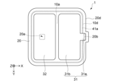
- FIG. 2 is a schematic top view of the light-emitting element according to the first embodiment.
- FIG. 2 is a schematic bottom view of the light-emitting element according to the first embodiment.
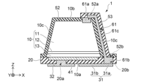
- FIG. 2 is a schematic cross-sectional view taken along line II-II in FIG. 5A to 5C are schematic cross-sectional views for explaining a step of the method for manufacturing the light-emitting element according to the first embodiment.
- 5A to 5C are schematic cross-sectional views for explaining a step of the method for manufacturing the light-emitting element according to the first embodiment.
- 5A to 5C are schematic cross-sectional views for explaining a step of the method for manufacturing the light-emitting element according to the first embodiment.
- 5A to 5C are schematic cross-sectional views for explaining a step of the method for manufacturing the light-emitting element according to the first embodiment.
- 5A to 5C are schematic cross-sectional views for explaining a step of the method for manufacturing the light-emitting element according to the first embodiment.
- 5A to 5C are schematic cross-sectional views for explaining a step of the method for manufacturing the light-emitting element according to the first embodiment.
- 5A to 5C are schematic cross-sectional views for explaining a step of the method for manufacturing the light-emitting element according to the first embodiment.
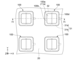
- 3A to 3C are schematic top views for explaining a step of the method for manufacturing the light-emitting element according to the first embodiment.
- 5A to 5C are schematic cross-sectional views for explaining a step of the method for manufacturing the light-emitting element according to the first embodiment.
- 5A to 5C are schematic cross-sectional views for explaining a step of the method for manufacturing the light-emitting element according to the first embodiment.
- 5A to 5C are schematic cross-sectional views for explaining a step of the method for manufacturing the light-emitting element according to the first embodiment.
- 5A to 5C are schematic cross-sectional views for explaining a step of the method for manufacturing the light-emitting element according to the first embodiment.
- 5A to 5C are schematic cross-sectional views for explaining a step of the method for manufacturing the light-emitting element according to the first embodiment.
- 5A to 5C are schematic cross-sectional views for explaining a step of the method for manufacturing the light-emitting element according to the first embodiment.
- 5A to 5C are schematic cross-sectional views for explaining a step of the method for manufacturing the light-emitting element according to the first embodiment.
- FIG. 5 is a schematic cross-sectional view of a light-emitting element according to a second embodiment.
- 10A to 10C are schematic cross-sectional views illustrating a step of a method for manufacturing a light-emitting element according to a second embodiment.
- 10A to 10C are schematic cross-sectional views illustrating a step of a method for manufacturing a light-emitting element according to a second embodiment.
- 13 is a schematic bottom view of a light-emitting element according to a third embodiment.
- 21B is a schematic cross-sectional view taken along line XXIB-XXIB of FIG. 21A.
- 13A to 13C are schematic cross-sectional views for explaining a step of a method for manufacturing a light-emitting element according to a third embodiment.
- 13A to 13C are schematic cross-sectional views for explaining a step of a method for manufacturing a light-emitting element according to a third embodiment.
- 13A to 13C are schematic cross-sectional views for explaining a step of a method for manufacturing a light-emitting element according to a third embodiment.
- 13A to 13C are schematic cross-sectional views for explaining a step of a method for manufacturing a light-emitting element according to a third embodiment.
- the positional relationship expressed as "above (or below)" includes, for example, when there are two members, a case in which the two members are in contact with each other, and a case in which the two members are not in contact with each other and one member is located above (or below) the other member.
- a member covering an object to be covered includes a case in which the member is in contact with the object to be covered and directly covers the object to be covered, and a case in which the member indirectly covers the object to be covered without contacting the object to be covered.
- FIG. 1A A light-emitting element 1 according to a first embodiment will be described with reference to Figures 1A, 1B, and 2.
- a top view of the light-emitting element 1 shown in Figure 1A and a bottom view of the light-emitting element 1 shown in Figure 1B two directions perpendicular to each other are defined as a first direction X and a second direction Y.
- a direction perpendicular to the first direction X and the second direction Y is defined as a third direction Z.
- Figure 2 is a schematic cross-sectional view taken along line II-II in Figure 1.
- the light-emitting element 1 comprises a semiconductor structure 10, a first insulating film 20, a first electrode 31, a second electrode 32, a second insulating film 52, and a first wiring 61.
- the semiconductor structure 10 has a first surface 10b, a second surface 10a located on the opposite side of the first surface 10b in the third direction Z, and a side surface 10c connecting the first surface 10b and the second surface 10a.
- the semiconductor structure 10 has a first semiconductor layer 11 located on the first surface 10b side, a second semiconductor layer 13 located on the second surface 10a side, and an active layer 12 located between the first semiconductor layer 11 and the second semiconductor layer 13.
- the active layer 12 is a light-emitting layer that emits light, and has, for example, a multiple quantum well (MQW) structure including a plurality of barrier layers and a plurality of well layers.
- MQW multiple quantum well
- the active layer 12 emits light having, for example, a peak wavelength of 210 nm or more and 580 nm or less.
- the first semiconductor layer 11 has a semiconductor layer including an n-type impurity
- the second semiconductor layer 13 has a semiconductor layer including a p-type impurity.
- Light emitted by the active layer 12 is emitted to the outside of the semiconductor structure 10 mainly from the first surface 10b and the side surface 10c.
- the first semiconductor layer 11 does not have a portion exposed from the second semiconductor layer 13 and the active layer 12.
- the active layer 12 is in contact with the entire surface of the first semiconductor layer 11 located opposite the first surface 10b. This allows the area of the active layer 12 to be larger in a planar view than when the first semiconductor layer 11 has an opening on the second surface 10a side that exposes a portion of the first semiconductor layer 11 from the second semiconductor layer 13 and the active layer 12, thereby improving the brightness of the light-emitting element 1.
- the first surface 10b is a surface of the first semiconductor layer 11 located on the opposite side to the active layer 12.
- the second surface 10a is a surface of the second semiconductor layer 13 located on the opposite side to the active layer 12.
- the side surface 10c of the semiconductor structure 10 includes the side surface of the first semiconductor layer 11, the side surface of the active layer 12, and the side surface of the second semiconductor layer 13. In a planar view, the area of the second surface 10a is larger than the area of the first surface 10b.
- the active layer 12 is located closer to the second surface 10a than the first surface 10b.
- the area of the second surface 10a is larger than the area of the first surface 10b in a planar view
- the area of the active layer 12 in a planar view can be made larger than when the area of the first surface 10b is larger than the area of the second surface 10a in a planar view.
- the first surface 10b and the side surface 10c form an obtuse angle
- the second surface 10a and the side surface 10c form an acute angle, so that the side surface 10c is inclined with respect to the first surface 10b and the second surface 10a.
- the shape of the outer edge 10d of the semiconductor structure 10 is, for example, a square shape. Furthermore, the outer edge 10d is the outer edge of the second surface 10a.
- the length of one side of the outer edge 10d is, for example, 5 ⁇ m or more and 150 ⁇ m or less.
- the corners of the outer edge 10d can be rounded, and in that case, the length of one side of the outer edge 10d is the length of the straight portion of that side of the outer edge 10d.
- the semiconductor structure 10 is made of a nitride semiconductor.
- nitride semiconductor includes all compositions in which the composition ratios x and y are changed within the respective ranges in the chemical formula In x Al y Ga 1-x-y N (0 ⁇ x ⁇ 1, 0 ⁇ y ⁇ 1, x+y ⁇ 1).
- those that further include a Group V element other than N (nitrogen) and those that further include various elements added to control various physical properties such as the conductivity type are also included in the "nitride semiconductor".
- the first insulating film 20 is disposed on the second surface 10a of the semiconductor structure 10 and covers the second surface 10a. As shown in FIG. 1B, the first insulating film 20 has a first opening 20a disposed at a position overlapping the second surface 10a of the semiconductor structure 10 in a plan view. In the example shown in FIG. 1B, the first insulating film 20 has one first opening 20a, but the first insulating film 20 may have a plurality of first openings 20a. In a plan view, an outer edge 20d of the first insulating film 20 is located outside the outer edge 10d of the semiconductor structure 10. In addition, the first insulating film 20 has a second opening 20b in a portion located outside the outer edge 10d of the semiconductor structure 10.
- the first insulating film 20 for example, a silicon oxide film or a silicon nitride film can be used.
- the first insulating film 20 can also include a dielectric multilayer film.
- the light directed from the active layer 12 toward the second surface 10a can be reflected by the dielectric multilayer film and directed toward the first surface 10b and the side surface 10c. This can improve the brightness of the light emitting element 1.
- the reflectance of the dielectric multilayer film with respect to the peak wavelength of the light emitted by the active layer 12 is, for example, 60% or more, preferably 70% or more.
- the first insulating film 20 can include, as the dielectric multilayer film, for example, SiO 2 layers and Nb 2 O 5 layers alternately stacked.
- pairs of Nb 2 O 5 layers having a thickness of 10 nm or more and 100 nm or less and SiO 2 layers having a thickness of 10 nm or more and 100 nm or less can be formed with a number of pairs of 2 to 6.
- the first electrode 31 is disposed on the first insulating film 20.
- the first electrode 31 is not connected to the second surface 10a of the semiconductor structure 10.
- the first insulating film 20 is located between the first electrode 31 and the second surface 10a.
- the first electrode 31 has a first portion 31a located outside the outer edge 10d of the semiconductor structure 10 in a plan view. As will be described later, the first electrode 31 is electrically connected to the first semiconductor layer 11 via a first wiring 61.
- the first electrode 31 can be, for example, a single metal layer containing Ti, Rh, Au, Pt, Al, Ag, Rh, or Ru, or a laminate structure containing at least two of these metal layers.
- the second electrode 32 is disposed on the first insulating film 20. As shown in FIG. 1B, the second electrode 32 is separated from the first electrode 31. As shown in FIG. 2, a part of the second electrode 32 is disposed in the first opening 20a of the first insulating film 20. The second electrode 32 is electrically connected to the second semiconductor layer 13 at the first opening 20a on the second surface 10a of the semiconductor structure 10.
- FIG. 2 shows an example in which the second electrode 32 is electrically connected to the second semiconductor layer 13 via a conductive layer 41 described later. Alternatively, the second electrode 32 may be electrically connected to the second semiconductor layer 13 by directly contacting the second semiconductor layer 13 at the first opening 20a.
- the second electrode 32 can be a single metal layer of the same material as the first electrode 31, or a laminated structure including at least two of these metal layers.
- the second insulating film 52 is disposed on the first surface 10b and the side surface 10c of the semiconductor structure 10.
- the second insulating film 52 covers the first surface 10b and the side surface 10c.
- the second insulating film 52 is disposed on a portion of the first insulating film 20 that is located outside the outer edge 10d of the semiconductor structure 10 in a plan view.
- the transmittance of the second insulating film 52 for the peak wavelength of the light emitted by the active layer 12 is, for example, 60% or more, preferably 70% or more.
- a silicon oxide film or a silicon nitride film can be used as the second insulating film 52.
- the second insulating film 52 has a third opening 52a located above the first surface 10b of the semiconductor structure 10.
- the third opening 52a may be located above the side surface 10c of the semiconductor structure 10.
- the second insulating film 52 also has a fourth opening 52b located above the second opening 20b of the first insulating film 20.
- the first wiring 61 is arranged on the second insulating film 52 and electrically connects a portion of the first semiconductor layer 11 exposed from the second insulating film 52 in the third opening 52a to a first portion 31a of the first electrode 31 exposed from the first insulating film 20 in the second opening 20b.
- the first wiring 61 is disposed in the third opening 52a of the second insulating film 52 and has a first connection portion 61a electrically connected to the first semiconductor layer 11 on the first surface 10b. When the third opening 52a is located above the side surface 10c of the semiconductor structure 10, the first wiring 61 is electrically connected to the first semiconductor layer 11 on the side surface 10c.
- the first wiring 61 is also disposed in the second opening 20b of the first insulating film 20 and has a second connection portion 61b electrically connected to the first portion 31a of the first electrode 31.
- the first wiring 61 also has an intermediate portion 61c that connects the first connection portion 61a and the second connection portion 61b and is located on the second insulating film 52 covering the side surface 10c of the semiconductor structure 10.
- the lower end of the intermediate portion 61c is disposed in the fourth opening 52b of the second insulating film 52 and is connected to the second connection portion 61b.
- the intermediate portion 61c is in contact with the second insulating film 52.
- the first wiring 61 is made of a transparent conductive film or a metal film.
- the light-emitting element 1 can be arranged on the wiring board with the second surface 10a side of the semiconductor structure 10 facing the wiring board.
- the first electrode 31 and the second electrode 32 arranged on the second surface 10a side can be electrically connected to the conductive part of the wiring board via a connecting member such as solder.
- the second electrode 32 is electrically connected to the second semiconductor layer 13 on the second surface 10a side through the first opening 20a of the first insulating film 20.
- the first electrode 31 is not electrically connected to the first semiconductor layer 11 on the second surface 10a side, but is electrically connected to the first semiconductor layer 11 on the first surface 10b side through the first wiring 61. Therefore, since the semiconductor structure 10 is electrically connected to the first electrode 31 and the second electrode 32 without removing the active layer 12, the area of the active layer 12 in a plan view can be made large, and the brightness of the light-emitting element 1 can be improved.
- the first semiconductor layer 11 is electrically connected to the conductive portion of the wiring board via the first wiring 61 arranged on the second insulating film 52 covering the side surface 10c of the semiconductor structure 10, and the first electrode 31 arranged on the second surface 10a side.
- the area of the region for arranging and connecting the light-emitting element to the wiring board can be reduced compared to the reference example. This makes it possible to miniaturize a light-emitting device including the light-emitting element and the wiring board. It also becomes easier to arrange multiple light-emitting elements on the wiring board at high density.
- the width of the first wiring 61 in the second direction Y is smaller than the width of the first surface 10b in the second direction Y and the width of the side surface 10c in the second direction Y. This reduces the absorption of the light emitted by the active layer 12 in the first wiring 61, and improves the brightness of the light-emitting element 1.
- the area of the first connection portion 61a in a plan view is preferably 1% to 20% of the area of the first surface 10b. By making the first connection portion 61a have such an area, it is possible to reduce the absorption of light emitted by the active layer 12 by the first wiring 61. In addition, it is preferable that the width of the intermediate portion 61c in the second direction Y is smaller than the width of the first connection portion 61a in the second direction Y. This makes it possible to reduce the absorption of light emitted by the active layer 12 by the intermediate portion 61c.
- the width of the intermediate portion 61c in the second direction Y is smaller than the width of the first connection portion 61a in the second direction Y, for example, the width of the intermediate portion 61c in the second direction Y is 5% to 50% of the width of the first connection portion 61a in the second direction Y.
- the first wiring 61 is made of a translucent conductive film. This makes it possible to reduce the absorption of light emitted by the active layer 12 in the first wiring 61, and improve the brightness of the light-emitting element 1.
- Examples of materials that can be used for the translucent conductive film of the first wiring 61 include indium tin oxide (ITO), zinc oxide (ZnO), and indium oxide ( In2O3 ).
- the transmittance of the translucent conductive film for the peak wavelength of the light emitted by the active layer 12 is, for example, 60% or more, and preferably 70% or more. Furthermore, a translucent conductive film using these materials can reduce the contact resistance with the semiconductor structure 10 on the first surface 10b, compared to a case where a metal film is used.
- the configuration of this embodiment in which the active layer 12 is not removed has a significant effect of ensuring a large area in a planar view of the active layer 12 when, for example, the length of one side in a planar view of the light-emitting element 1 is 100 ⁇ m or less, making it easier to improve brightness.
- the first electrode 31 further has a second portion 31b located inside the outer edge 10d of the semiconductor structure 10 in a plan view.
- the second portion 31b and the first portion 31a can be integrally formed of the same material. Since the first electrode 31 has the second portion 31b located inside the outer edge 10d of the semiconductor structure 10 in a plan view, the area of the first electrode 31 can be increased while reducing the size of the light-emitting element 1 in a plan view. By increasing the area of the first electrode 31 in a plan view, the contact area between the first electrode 31 and the conductive portion of the wiring board can be increased, and the forward voltage of the light-emitting element 1 can be reduced. In addition, the heat generated by the semiconductor structure 10 can be easily dissipated to the wiring board via the second portion 31b.
- the second portion 31b overlaps the second surface 10a of the semiconductor structure 10 in a plan view.
- the area of the first electrode 31 having the first portion 31a and the second portion 31b can be, for example, 80% to 120% of the area of the second electrode 32. In this way, the difference between the area of the first electrode 31 and the area of the second electrode 32 in a plan view can be reduced, and misalignment that occurs when the light-emitting element 1 is placed on a wiring board via a connecting member such as solder can be reduced.
- the area of the first portion 31a located outside the outer edge 10d of the semiconductor structure 10 is preferably smaller than the area of the second portion 31b. This allows the size of the light-emitting element 1 to be reduced.
- the area of the second portion 31b is larger than the area of the first portion 31a, which improves the ease of arrangement of the light-emitting element 1 on the wiring board, the effect of reducing the forward voltage, and the heat dissipation effect, as described above.
- the area of the first portion 31a is, for example, 5% to 20% of the area of the second portion 32b.
- the sum of the area of the second portion 31b and the area of the second electrode 32 is preferably 60% to 90% of the area of the second surface 10a.
- the light-emitting element 1 may further include a conductive layer 41 disposed on the second surface 10a of the semiconductor structure 10.
- the conductive layer 41 is electrically connected to the second semiconductor layer 13 on the second surface 10a.
- the conductive layer 41 is covered with the first insulating film 20. A portion of the conductive layer 41 is exposed from the first insulating film 20 in the first opening 20a and is electrically connected to the second electrode 32.
- the outer edge 41a of the conductive layer 41 is located inside the outer edge 10d of the semiconductor structure 10.
- the area of the conductive layer 41 is larger than the area of the first opening 20a.
- the conductive layer 41 makes it easier to diffuse the current supplied through the second electrode 32 in the surface direction of the second semiconductor layer 13.
- a transparent conductive film can be used as the material of the conductive layer 41 .
- the transparent conductive film for example, ITO, ZnO, In 2 O 3, etc. can be used.
- a metal material may be used as the material of the conductive layer 41.
- the metal material of the conductive layer 41 for example, a material similar to the material used for the first electrode 31 can be used. By using these materials, it is possible to easily reflect light from the active layer 12 compared to the case where a transparent conductive film is used, and the light extraction efficiency of the light-emitting element 1 can be improved.
- the light emitting element 1 can further include a third insulating film 53.
- the third insulating film 53 covers the first wiring 61.
- As the third insulating film 53 for example, a silicon oxide film or a silicon nitride film can be used.
- the method for manufacturing the light-emitting element according to the first embodiment includes the steps of preparing a wafer, bonding the wafer to a second substrate, exposing an upper surface of the first semiconductor layer, separating the semiconductor structure into a plurality of light-emitting sections, forming a second insulating film, exposing a first portion of the first electrode from the first insulating film and exposing a portion of the first semiconductor layer from the second insulating film, forming a first wiring, and separating the light-emitting section from the second substrate.
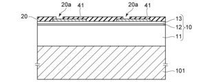
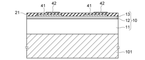
- ⁇ Wafer Preparation Step> 6 shows a portion of a wafer W.
- the wafer W has a first substrate 101, a semiconductor structure 10, a first insulating film 20, a first electrode 31, and a second electrode 32.
- an insulating substrate such as sapphire or spinel (MgAl 2 O 4 ) having any one of the C-plane, R-plane, and A-plane as the main surface can be used.
- a conductive substrate such as SiC (including 6H, 4H, and 3C), ZnS, ZnO, GaAs, and Si can be used.
- a sapphire substrate having the C-plane as the main surface is used for the first substrate 101.
- the semiconductor structure 10 is disposed on the main surface of the first substrate 101.
- the semiconductor structure 10 has a first semiconductor layer 11, a second semiconductor layer 13 that is farther from the first substrate 101 than the first semiconductor layer, and an active layer 12 that is located between the first semiconductor layer 11 and the second semiconductor layer 13.
- the surface of the first semiconductor layer 11 facing the active layer 12 does not have any portion exposed from the second semiconductor layer 13 and the active layer 12. This allows the area of the active layer 12 to be increased in a plan view, as described above.
- the metal contained in the first electrode 31 or the second electrode 32 is ionized in the liquid, and the occurrence of metal migration due to the potential difference between a portion (exposed portion) of the first semiconductor layer 11 and the second semiconductor layer 13 can be reduced. Therefore, it is possible to make it difficult for metal to deposit in unintended areas, and the reliability of the light-emitting device can be improved.
- the first insulating film 20 is disposed on the second semiconductor layer 13 and has a first opening 20a located above the second semiconductor layer 13.
- the first electrode 31 is disposed on the first insulating film 20.
- the second electrode 32 is disposed on the first insulating film 20 at a distance from the first electrode 31 and is electrically connected to the second semiconductor layer 13 through the first opening 20a.
- the wafer W may further have a conductive layer 41 disposed on the second semiconductor layer 13 and electrically connected to the second electrode 32.
- the wafer W shown in FIG. 6 can be purchased and prepared.
- the process of preparing the wafer W may also include the steps shown in Figures 3 to 6. Each step shown in Figures 3 to 6 will be described below.
- the semiconductor structure 10 is formed on the first substrate 101.
- the semiconductor structure 10 is formed by sequentially forming the first semiconductor layer 11, the active layer 12, and the second semiconductor layer 13 on the first substrate 101 by MOCVD (Metal Organic Chemical Vapor Deposition) method.
- MOCVD Metal Organic Chemical Vapor Deposition
- the process of removing a part of the second semiconductor layer 13 and a part of the active layer 12 to expose a part of the first semiconductor layer 11 from the second semiconductor layer 13 and the active layer 12 is not performed.
- the process of preparing the wafer W can include a process of forming a conductive layer 41 on the second semiconductor layer 13, as shown in FIG. 4.
- the conductive layer 41 contacts the upper surface of the second semiconductor layer 13 and is electrically connected to the second semiconductor layer 13.
- the conductive layer 41 can be formed by, for example, a sputtering method or a vapor deposition method.
- the conductive layer 41 does not have to be formed. The following description will be given of the case where the conductive layer 41 is formed.
- the process of preparing the wafer W includes forming a first insulating film 20 having a first opening 20a located above the conductive layer 41 on the second semiconductor layer 13 and the conductive layer 41, as shown in FIG. 5. A portion of the conductive layer 41 is exposed from the first insulating film 20 at the first opening 20a.
- the first insulating film 20 can be formed, for example, by a chemical vapor deposition (CVD) method or a sputtering method.
- the first opening 20a can be formed, for example, by removing a portion of the first insulating film 20 by etching.
- the process of preparing the wafer W includes a process of forming a first electrode 31 and a second electrode 32, as shown in FIG. 6.
- the second electrode 32 is formed on the first insulating film 20 and in the first opening 20a, and is electrically connected to the conductive layer 41 in the first opening 20a.
- the second electrode 32 is electrically connected to the second semiconductor layer 13 via the conductive layer 41.
- the first electrode 31 is formed on the first insulating film 20, separated from the second electrode 32. In the process shown in FIG. 6, the first electrode 31 is not electrically connected to the first semiconductor layer 11.
- the first electrode 31 and the second electrode 32 can be formed, for example, by a sputtering method or a vapor deposition method.
- the first electrode 31 and the second electrode 32 can be formed simultaneously using the same material.
- the side of the wafer W on which the second electrode 32 and the first electrode 31 are arranged is bonded to the second substrate 102 via a bonding member 51.
- the top and bottom positions of the wafer W shown in Fig. 7 are shown opposite to the top and bottom positions of the wafer W shown in Fig. 6.
- the bonding member 51 is disposed between the first insulating film 20 and the second substrate 102.
- the bonding member 51 covers the first electrode 31 and the second electrode 32.
- a resin member mainly composed of epoxy resin, acrylic resin, or polyimide resin can be used as the bonding member 51.
- a substrate similar to the first substrate 101 can be used as the second substrate 102.
- the first substrate 101 is removed to expose the upper surface 11a of the first semiconductor layer 11 as shown in Fig. 8.
- the first substrate 101 can be removed by, for example, a laser lift off (LLO) method, grinding, polishing, etching, or other method.
- LLO laser lift off
- Fig. 9 is a schematic cross-sectional view taken along line IX-IX in Fig. 10.
- the semiconductor structure 10 is separated into a plurality of light emitting sections 100 so that the first electrode 31 has a first portion 31a located outside the outer edge 100d of the light emitting section 100 in a planar view.
- the semiconductor structure 10 that overlaps a part of the first electrode 31 (the part that becomes the first portion 31a) in a planar view is removed.
- a portion of the semiconductor structure 10 is removed, exposing the upper surface of the first insulating film 20 from the semiconductor structure 10 (light emitting portion 100).
- a groove extending in the first direction X and the second direction Y is formed on the first insulating film 20, and the semiconductor structure 10 is separated into a plurality of light emitting portions 100 aligned in the first direction X and the second direction Y.
- a part of the semiconductor structure 10 can be removed by dry etching using a mask.
- the dry etching method is RIE (Reactive Ion Etching).
- RIE reactive Ion Etching
- a chlorine-containing gas such as Cl 2 or SiCl 4 can be used. Since the amount of etching is easier to control in dry etching than in wet etching, the shape of the light emitting portion 100 can be made into a desired shape by removing a part of the semiconductor structure 10 by dry etching. Alternatively, a part of the semiconductor structure 10 can be removed by wet etching using a mask.
- the light emitting unit 100 has an upper surface 100a, a lower surface 100c located on the opposite side of the upper surface 100a in the third direction Z, and a side surface 100b connecting the upper surface 100a and the lower surface 100c.
- the upper surface 100a of the light emitting unit 100 is the upper surface 11a of the first semiconductor layer 11.
- the lower surface 100c of the light emitting unit 100 is the lower surface of the second semiconductor layer 13.
- the side surface 100b of the light emitting unit 100 corresponds to the side surface 10c of the semiconductor structure 10 shown in FIG. 2.
- the area of the lower surface 100c of the light emitting unit 100 is larger than the area of the upper surface 100a of the light emitting unit 100.
- the side surface 100b of the light emitting unit 100 includes the side surface of the first semiconductor layer 11, the side surface of the active layer 12, and the side surface of the second semiconductor layer 13.
- the cross-sectional shape of the light-emitting section 100 can be made substantially trapezoidal.
- the active layer 12 is located closer to the bottom surface 100c than to the top surface 100a of the light-emitting section 100.
- the area of the bottom surface 100c of the light-emitting section 100 is larger than the area of the top surface 100a of the light-emitting section 100. Therefore, the light-emitting section 100 can have a larger area of the active layer 12 than when the area of the top surface 100a is larger than the area of the bottom surface 100c.
- the side surface 100b is inclined with respect to the top surface 100a.
- the angle between the side surface 100b and the bottom surface 100c is an acute angle
- the angle between the side surface 100b and the top surface 100a is an obtuse angle.
- a second insulating film 52 is formed to cover the light emitting portions 100, as shown in Fig. 11.
- the second insulating film 52 covers the upper surface 100a and the side surface 100b of the light emitting portion 100.
- the second insulating film 52 also covers the upper surface of the first insulating film 20 exposed from the light emitting portion 100.
- the second insulating film 52 does not have to cover the upper surface of the first insulating film 20.
- the second insulating film 52 can be formed by, for example, a CVD method or a sputtering method.
- Step of exposing a first portion of a first electrode from a first insulating film and exposing a part of a first semiconductor layer from a second insulating film After the process of forming the second insulating film 52, as shown in FIG. 12 , a portion of the first insulating film 20 is removed to expose the first portion 31 a of the first electrode 31 from the first insulating film 20, and a portion of the second insulating film 52 is removed to expose a portion of the first semiconductor layer 11 of the light emitting portion 100 from the second insulating film 52.
- a part of the first insulating film 20 and a part of the second insulating film 52 can be removed by RIE using a mask.
- a gas containing fluorine can be used as the gas in the RIE method.
- a third opening 52a is formed in the second insulating film 52.
- a portion of the upper surface 11a of the first semiconductor layer 11 is exposed from the second insulating film 52.
- the third opening 52a may be formed in the second insulating film 52 at a position where the side surface 10c is exposed.
- a second opening 20b is formed in the first insulating film 20.
- the first portion 31a of the first electrode 31 is exposed from the first insulating film 20.
- the second insulating film 52 covers the upper surface of the first insulating film 20, before forming the second opening 20b in the first insulating film 20, a part of the second insulating film 52 located above the first portion 31a of the first electrode 31 is removed to form a fourth opening 52b in the second insulating film 52. After forming the fourth opening 52b in the second insulating film 52, a part of the first insulating film 20 exposed from the second insulating film 52 in the fourth opening 52b is removed to form the second opening 20b below the fourth opening 52b. The first portion 31a of the first electrode 31 is exposed from the first insulating film 20 and the second insulating film 52 in the second opening 20b and the fourth opening 52b.
- a first wiring 61 is formed on the second insulating film 52 as shown in Fig. 13.
- the first wiring 61 can be formed by a sputtering method or a vapor deposition method.
- the first wiring 61 electrically connects a portion of the first semiconductor layer 11 exposed from the second insulating film 52 to the first portion 31a of the first electrode 31 exposed from the first insulating film 20. This makes it possible to electrically connect the first electrode 31 arranged on the lower surface 100c side of the light emitting section 100 to the first semiconductor layer 11 on the upper surface 11a side of the first semiconductor layer 11, even if a portion of the first semiconductor layer 11 is not exposed from the second semiconductor layer 13 and the active layer 12 on the lower surface 100c side of the light emitting section 100.
- the first connection portion 61a of the first wiring 61 is electrically connected to the upper surface 11a of the first semiconductor layer 11.
- the first wiring 61 is electrically connected to the first semiconductor layer 11 at the side surface 10c.
- the second connection portion 61b of the first wiring 61 is electrically connected to the first portion 31a of the first electrode 31.
- the intermediate portion 61c that connects the first connection portion 61a and the second connection portion 61b of the first wiring 61 is formed on the second insulating film 52 that covers the side surface 100b of the light emitting portion 100. The intermediate portion 61c is in contact with the second insulating film 52.
- the method for manufacturing the light-emitting element according to the first embodiment may include a step of forming a third insulating film 53 that covers the first wiring 61, as shown in Fig. 14.
- the third insulating film 53 can be formed by, for example, a CVD method or a sputtering method.
- Step of separating the light emitting section and the second substrate After the first wiring 61 is formed, the light emitting section 100 is separated from the second substrate 102.
- the process of separating the light emitting section 100 from the second substrate 102 can include the steps shown in FIGS.
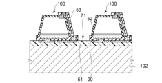
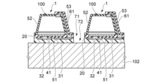
- the first insulating film 20 located in the region between the light-emitting sections 100 in a plan view is removed to form a first groove 71 in the first insulating film 20 as shown in FIG. 15.
- the upper surface of the joining member 51 is exposed from the second insulating film 52 and the first insulating film 20.
- the second insulating film 52 is also disposed in the region between the light-emitting sections 100 in a plan view, the first insulating film 20 is removed after the second insulating film 52 is removed.
- the second insulating film 52 can be removed using a method similar to that used to remove the first insulating film 20.
- each light-emitting element 1 has a light-emitting portion 100, a first electrode 31, a second electrode 32, a first insulating film 20, a second insulating film 52, and a first wiring 61. Furthermore, the light-emitting element 1 can have a conductive layer 41 and a third insulating film 53, as necessary.
- the first groove 71 and the second groove 72 can be formed by, for example, the RIE method. After the first groove 71 is formed by the RIE method, the gas can be switched and the second groove 72 can be formed by the RIE method.
- the first groove 71 can be formed by, for example, the RIE method using a gas containing fluorine.
- the second groove 72 can be formed by, for example, the RIE method using a gas containing oxygen.
- the first groove 71 and the second groove 72 may be formed successively by the RIE method using the same gas.
- the light-emitting element 1 is supported on the second substrate 102 via a bonding member 51.
- the light-emitting element 1 can be separated from the second substrate 102 by irradiating the second substrate 102 with laser light to remove the bonding member 51.
- the upper surface 100a of the light-emitting portion 100 in the light-emitting element 1 separated from the second substrate 102 is bonded to, for example, an adhesive support member 103.
- the light-emitting element 1 may be separated from the second substrate 102 after being bonded to the support member 103.
- the bonding member 51 may be removed by, for example, an RIE method to expose the first electrode 31 and the second electrode 32.
- the first electrode 31 and the second electrode 32 function as external connection terminals bonded to the conductive portion of the wiring substrate.
- the semiconductor structure 10 can be separated into a plurality of light-emitting sections 100 so that the first electrode 31 has a second portion 31b located inside the outer edge 100d of the light-emitting section 100 in a plan view.
- This allows the area of the first electrode 31 to be increased while reducing the size of the light-emitting element.
- the forward voltage can be reduced and the heat dissipation effect can be improved.
- the area of the first portion 31a is smaller than the area of the second portion 31b. This allows the size of the light-emitting element to be reduced.
- the area of the second portion 31b is larger than the area of the first portion 31a, which improves the ease of arranging the light-emitting element on the wiring board, the effect of reducing the forward voltage, and the heat dissipation effect, as described above.
- the first wiring 61 it is preferable to form the first wiring 61 from a light-transmitting conductive film. This makes it possible to reduce absorption of light emitted by the active layer 12 in the first wiring 61.
- FIG. 18 is a schematic cross-sectional view of a light-emitting element 2 according to the second embodiment.
- the first surface 10b of the semiconductor structure 10 includes a plurality of protrusions 10b1
- the side surface 10c of the semiconductor structure 10 includes a plurality of protrusions 10c1. This can improve the light extraction efficiency from the first surface 10b and the side surface 10c.
- the arithmetic mean height of the first surface 10b which includes multiple convex portions 10b1
- a convex portion shaped along the convex portion 10b1 is formed on the surface of the second insulating film 52 covering the first face 10b, and a convex portion shaped along the convex portion 10c1 of the side face 10c is formed on the surface of the second insulating film 52 covering the side face 10c. This can improve the extraction efficiency of light extracted from the first face 10b and the side face 10c through the second insulating film 52.
- a convex portion shaped along the convex portion 10c1 is formed on the surface of the first wiring 61 arranged on the second insulating film 52 covering the side face 10c and on the surface of the third insulating film 53 covering the first wiring 61. This can improve the extraction efficiency of light extracted from the side face 10c through the first wiring 61 and the third insulating film 53.
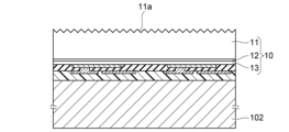
- the upper surface 11a of the first semiconductor layer 11 is roughened before the semiconductor structure 10 is separated into a plurality of light emitting units 100 as shown in Fig. 19.
- the upper surface 11a of the first semiconductor layer 11 can be roughened by dry etching using a chlorine-containing gas such as Cl2 or SiCl4 , or by wet etching using an alkaline solution such as TMAH (tetramethylammonium hydroxide).
- a part of the semiconductor structure 10 is removed to separate the semiconductor structure 10 into a plurality of light emitting units 100.
- a mask placed on the upper surface 11a of the first semiconductor layer 11 is used to remove a part of the semiconductor structure 10 by dry etching.
- the dry etching method for example, the RIE method can be used.
- a gas containing chlorine such as Cl 2 or SiCl 4 can be used. Dry etching has good etching controllability, and it is easy to make the shape of the light emitting unit 100 after etching into a desired shape.
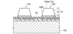
- the dry etching proceeds from the roughened upper surface 11a of the first semiconductor layer 11 exposed from the mask. Therefore, the surface roughness of the dry etched surface of the semiconductor structure 10 is greater than when the upper surface 11a is not roughened in advance. Therefore, as shown in FIG. 20, the side surface 100b of the light emitting portion 100 exposed by removing a portion of the semiconductor structure 10 can be roughened. This allows the process of separating the semiconductor structure 10 into a plurality of light emitting portions 100 and the roughening of the side surface 100b of the light emitting portion 100 to be performed in a single process, so that light emitting devices with improved light extraction efficiency can be efficiently manufactured.
- the side surface 100b of the light emitting portion 100 exposed by removing a portion of the semiconductor structure 10 shown in FIG. 20 corresponds to the side surface 10c of the semiconductor structure 10 in the light emitting element 2 shown in FIG. 18.
- a portion of the semiconductor structure 10 may be removed by wet etching to separate it into the light emitting portion 100. Compared to dry etching, wet etching makes it easier to increase the surface roughness of the side surface 10c and improve the efficiency of extracting light from the side surface 10c.
- the upper surface 100a and the side surface 100b of the light emitting portion 100 are roughened as shown in FIG. 20.
- the top surface 100a and the side surface 100b of the light emitting portion 100 are roughened by dry etching using a chlorine-containing gas or wet etching using an alkaline solution such as TMAH.
- the top surface 100a and the side surface 100b of the light emitting portion 100 can be roughened in a single process, so that a light emitting element with improved light extraction efficiency can be efficiently manufactured.
- the top surface 100a and the side surface 100b of the light emitting portion 100 in FIG. 20 correspond to the first surface 10b and the side surface 10c, respectively, of the semiconductor structure 10 in the light emitting element 2 shown in FIG. 18.
- the semiconductor structure 10 is removed while the upper surface 11a of the first semiconductor layer 11 is not roughened, and the semiconductor structure 10 is separated into a plurality of light emitting sections 100.
- the upper surface 11a of the first semiconductor layer 11, which becomes the first surface 100a of the light emitting section 100 is etched while having a high degree of flatness, so that it is easier to shape the light emitting section 100 into the desired shape.
- the crystal orientation of the upper surface 100a of the light emitting portion 100 is different from that of the side surface 100b of the light emitting portion 100. Therefore, after separation into the light emitting portions 100, a roughening process is performed on the upper surface 100a and the side surface 100b of the light emitting portion 100, so that the surface roughness of the upper surface 100a of the light emitting portion 100 can be made larger than the surface roughness of the side surface 100b of the light emitting portion 100. This makes it easier for light to be extracted from the first surface 10b than from the side surface 10c of the semiconductor structure 10 in the light emitting element 2, and light distribution characteristics with high directivity in the direction directly above the first surface 10b can be obtained.
- Fig. 21A is a schematic bottom view of the light-emitting element 3 according to the third embodiment.
- Fig. 21B is a schematic cross-sectional view taken along line XXIB-XXIB in Fig. 21A.
- the light-emitting element 3 further includes a reflective film 42 disposed between the second semiconductor layer 13 and the second electrode 32.
- the reflective film 42 is reflective to the light emitted by the active layer 12.
- a metal can be used as the material of the reflective film 42.
- the reflective film 42 can include, for example, an Al film, a Ti film, or a laminated structure thereof.
- the light traveling from the active layer 12 toward the second surface 10a of the semiconductor structure 10 can be reflected by the reflective film 42 and directed toward the first surface 10b and the side surface 10c. This can improve the brightness of the light-emitting element 3.
- the reflectance of the reflective film 42 for the peak wavelength of the light emitted by the active layer 12 is, for example, 60% or more, preferably 70% or more.
- the reflective film 42 can be disposed, for example, between the conductive layer 41 and the second portion 31b.
- the first insulating film 20 is located between the reflective film 42 and the conductive layer 41, between the reflective film 42 and the second electrode 32, and between the reflective film 42 and the second portion 31b of the first electrode 31.
- a reflective film 42 is formed on the first layer 21.
- the reflective film 42 can be formed by, for example, a sputtering method or a vapor deposition method.
- the structure of the light-emitting element 2 of the second embodiment and the structure of the light-emitting element 3 of the third embodiment can be combined to form a light-emitting element having a semiconductor structure 10 including a roughened first surface 10b and side surface 10c, and a reflective film 42.
- Embodiments of the present invention include the following light-emitting device manufacturing method and light-emitting device.
- a step of preparing a wafer including: a first substrate; a semiconductor structure disposed on the first substrate, the semiconductor structure having a first semiconductor layer, a second semiconductor layer located farther from the first substrate than the first semiconductor layer, and an active layer located between the first semiconductor layer and the second semiconductor layer; a first insulating film disposed on the second semiconductor layer and having an opening located above the second semiconductor layer; a first electrode disposed on the first insulating film; and a second electrode disposed on the first insulating film and spaced apart from the first electrode, electrically connecting to the second semiconductor layer through the opening; bonding the side of the wafer on which the second electrode and the first electrode are disposed to a second substrate; removing the first substrate after bonding the wafer and the second substrate to expose an upper surface of the first semiconductor layer; a step of removing a portion of the semiconductor structure from the upper surface side of the first semiconductor layer and dividing the semiconductor structure into a plurality of light emitting sections, the step of dividing the semiconductor structure into the plurality of light
- the wafer further includes a reflective film disposed between the conductive layer and the second electrode.
- Item 9 Item 9. The method for manufacturing a light-emitting element according to item 8, wherein an area of the reflective film is 60% to 90% of an area of the conductive layer in a plan view.
- a semiconductor structure having a first surface, a second surface located on the opposite side of the first surface, and a side surface connecting the first surface and the second surface, the semiconductor structure having a first semiconductor layer located on the first surface side, a second semiconductor layer located on the second surface side, and an active layer located between the first semiconductor layer and the second semiconductor layer; a first insulating film disposed on the second surface and having an opening disposed at a position overlapping the second surface in a plan view; a first electrode disposed on the first insulating film and not connected to the second surface, the first electrode having a first portion located outside an outer edge of the semiconductor structure in a plan view; a second electrode disposed on the first insulating film and spaced apart from the first electrode, and electrically connected to the second semiconductor layer on the second surface through the opening; a second insulating film disposed on the first surface and the side surface of the semiconductor structure; a first wiring disposed on the second insulating film and electrically connecting a part of the first semiconductor layer exposed from the second
- the light-emitting element according to item 10 wherein the first electrode has a second portion located inside the outer edge of the semiconductor structure in a plan view.
- Item 12 Item 12.
- Item 13 Item 13.
- Item 14 Item 14.
- the light-emitting device according to item 16, further comprising a reflective film disposed between the conductive layer and the second electrode.
- Item 18 Item 18.
Landscapes
- Led Devices (AREA)
Abstract
Description
(発光素子)
図1A、図1B、及び図2を参照して、第1実施形態に係る発光素子1について説明する。図1Aに示す発光素子1の上面視及び図1Bに示す発光素子1の下面視において、互いに直交する2つの方向を第1方向X及び第2方向Yとする。また、第1方向X及び第2方向Yに直交する方向を第3方向Zとする。図2は、図1のII-II線における模式断面図である。
半導体構造体10は、第1面10bと、第3方向Zにおいて第1面10bの反対側に位置する第2面10aと、第1面10bと第2面10aとを接続する側面10cとを有する。半導体構造体10は、第1面10b側に位置する第1半導体層11と、第2面10a側に位置する第2半導体層13と、第1半導体層11と第2半導体層13との間に位置する活性層12とを有する。活性層12は、光を発する発光層であり、例えば複数の障壁層と、複数の井戸層を含むMQW(Multiple Quantum well)構造を有する。活性層12は、例えば、ピーク波長が210nm以上580nm以下の光を発する。例えば、第1半導体層11はn型不純物を含む半導体層を有し、第2半導体層13はp型不純物を含む半導体層を有する。活性層12が発する光は、主に、第1面10b及び側面10cから半導体構造体10の外部に出射する。
第1絶縁膜20は、半導体構造体10の第2面10a上に配置され、第2面10aを覆っている。図1Bに示すように、第1絶縁膜20は、平面視において、半導体構造体10の第2面10aと重なる位置に配置される第1開口20aを有する。図1Bに示す例では第1絶縁膜20は1つの第1開口20aを有するが、第1絶縁膜20は複数の第1開口20aを有してよい。平面視において、第1絶縁膜20の外縁20dは、半導体構造体10の外縁10dよりも外側に位置する。また、第1絶縁膜20は、半導体構造体10の外縁10dよりも外側に位置する部分に第2開口20bを有する。
図2に示すように、第1電極31は、第1絶縁膜20上に配置されている。第1電極31は、半導体構造体10の第2面10aと接続しない。第1電極31と第2面10aとの間に第1絶縁膜20が位置する。図1Bに示すように、第1電極31は、平面視において、半導体構造体10の外縁10dよりも外側に位置する第1部分31aを有する。後述するように、第1電極31は、第1配線61を介して第1半導体層11と電気的に接続する。
第2電極32は、第1絶縁膜20上に配置されている。図1Bに示すように、第2電極32は、第1電極31と離隔している。図2に示すように、第2電極32の一部は、第1絶縁膜20の第1開口20aに配置されている。第2電極32は、半導体構造体10の第2面10aにおいて、第2半導体層13と第1開口20aで電気的に接続する。図2には、第2電極32が、後述する導電層41を介して第2半導体層13と電気的に接続する例を示す。または、第2電極32は、第1開口20aにおいて第2半導体層13と直接接することで電気的に接続してもよい。
第2絶縁膜52は、半導体構造体10の第1面10b上及び側面10c上に配置されている。第2絶縁膜52は、第1面10b及び側面10cを覆っている。また、第2絶縁膜52は、第1絶縁膜20のうち平面視において半導体構造体10の外縁10dよりも外側に位置する部分の上に配置されている。活性層12が発する光のピーク波長に対する第2絶縁膜52の透過率は、例えば、60%以上、好ましくは70%以上である。第2絶縁膜52として、例えば、シリコン酸化膜またはシリコン窒化膜を用いることができる。
第1配線61は、第2絶縁膜52上に配置され、第3開口52aにおいて第2絶縁膜52から露出する第1半導体層11の一部と、第2開口20bにおいて第1絶縁膜20から露出する第1電極31の第1部分31aとを電気的に接続している。
図2に示すように、発光素子1は、半導体構造体10の第2面10aに配置された導電層41をさらに備えることができる。導電層41は、第2面10aにおいて第2半導体層13と電気的に接続されている。導電層41は、第1絶縁膜20に覆われている。導電層41の一部が、第1開口20aにおいて第1絶縁膜20から露出し、第2電極32と電気的に接続されている。
発光素子1は、第3絶縁膜53をさらに備えることができる。第3絶縁膜53は、第1配線61を覆っている。第3絶縁膜53として、例えば、シリコン酸化膜またはシリコン窒化膜を用いることができる。
図3~図17を参照して、第1実施形態に係る発光素子の製造方法について説明する。第1実施形態に係る発光素子の製造方法は、ウェハを準備する工程と、ウェハを第2基板に接合する工程と、第1半導体層の上面を露出させる工程と、半導体構造体を複数の発光部に分離する工程と、第2絶縁膜を形成する工程と、第1電極の第1部分を第1絶縁膜から露出させ且つ第1半導体層の一部を第2絶縁膜から露出させる工程と、第1配線を形成する工程と、発光部と第2基板とを分離する工程と、を備える。
図6は、ウェハWの一部分を表す。ウェハWは、第1基板101と、半導体構造体10と、第1絶縁膜20と、第1電極31と、第2電極32とを有する。
図7に示すように、ウェハWにおける第2電極32及び第1電極31が配置された側を、接合部材51を介して第2基板102に接合する。図7に示すウェハWの上下の位置は、図6に示すウェハWの上下の位置と逆に表している。
ウェハWと第2基板102とを接合する工程の後、第1基板101を除去し、図8に示すように、第1半導体層11の上面11aを露出させる。第1基板101は、例えば、LLO(Laser Lift Off)法、研削、研磨、エッチング等の方法によって除去することができる。
第1基板101を除去した後、露出した第1半導体層11の上面11a側から半導体構造体10の一部を除去し、図9及び図10に示すように、半導体構造体10を複数の発光部100に分離する。図9は、図10のIX-IX線における模式断面図である。
半導体構造体10を複数の発光部100に分離する工程の後、図11に示すように、発光部100を覆う第2絶縁膜52を形成する。第2絶縁膜52は、発光部100の上面100a及び側面100bを覆う。また、第2絶縁膜52は、発光部100から露出する第1絶縁膜20の上面を覆う。なお、第2絶縁膜52は、第1絶縁膜20の上面を覆わなくてもよい。第2絶縁膜52は、例えば、CVD法またはスパッタリング法により形成することができる。
第2絶縁膜52を形成する工程の後、図12に示すように、第1絶縁膜20の一部を除去し、第1電極31の第1部分31aを第1絶縁膜20から露出させ、且つ第2絶縁膜52の一部を除去し、発光部100の第1半導体層11の一部を第2絶縁膜52から露出させる。
第1電極31の第1部分31aを第1絶縁膜20から露出させ且つ第1半導体層11の一部を第2絶縁膜52から露出させる工程の後、図13に示すように、第2絶縁膜52上に第1配線61を形成する。例えば、スパッタリング法または蒸着法により、第1配線61を形成することができる。
第1配線61を形成した後、第1実施形態に係る発光素子の製造方法は、図14に示すように、第1配線61を覆う第3絶縁膜53を形成する工程を備えてもよい。第3絶縁膜53は、例えば、CVD法またはスパッタリング法により形成することができる。
第1配線61を形成した後、発光部100と第2基板102とを分離する。発光部100と第2基板102とを分離する工程は、図15~図17に示す工程を有することができる。
図18は、第2実施形態に係る発光素子2の模式断面図である。
図21Aは、第3実施形態に係る発光素子3の模式下面図である。図21Bは、図21AのXXIB-XXIB線における模式断面図である。
第1基板と、前記第1基板上に配置され、第1半導体層と、前記第1半導体層よりも前記第1基板から離れた第2半導体層と、前記第1半導体層と前記第2半導体層との間に位置する活性層とを有する半導体構造体と、前記第2半導体層上に配置され、前記第2半導体層の上方に位置する開口を有する第1絶縁膜と、前記第1絶縁膜上に配置された第1電極と、前記第1絶縁膜上に前記第1電極と離隔して配置され、前記第2半導体層と前記開口で電気的に接続する第2電極と、を有するウェハを準備する工程と、
前記ウェハにおける前記第2電極及び前記第1電極が配置された側を第2基板に接合する工程と、
前記ウェハと前記第2基板とを接合する工程の後、前記第1基板を除去し、前記第1半導体層の上面を露出させる工程と、
前記第1半導体層の前記上面側から前記半導体構造体の一部を除去し、前記半導体構造体を複数の発光部に分離する工程であって、平面視において前記第1電極が前記発光部の外縁よりも外側に位置する第1部分を有するように、前記半導体構造体を前記複数の発光部に分離する工程と、
前記発光部を覆う第2絶縁膜を形成する工程と、
前記第1絶縁膜の一部を除去し、前記第1電極の前記第1部分を前記第1絶縁膜から露出させ、且つ前記第2絶縁膜の一部を除去し、前記発光部の前記第1半導体層の一部を前記第2絶縁膜から露出させる工程と、
前記第2絶縁膜から露出する前記第1半導体層の前記一部と、前記第1絶縁膜から露出する前記第1電極の前記第1部分とを電気的に接続する第1配線を、前記第2絶縁膜上に形成する工程と、
前記第1配線を形成した後、前記発光部と前記第2基板とを分離する工程と、
を備える、発光素子の製造方法。
[項2]
前記半導体構造体を前記複数の発光部に分離する工程において、平面視において前記第1電極が前記発光部の前記外縁よりも内側に位置する第2部分を有するように、前記半導体構造体を前記複数の発光部に分離する、項1に記載の発光素子の製造方法。
[項3]
平面視において、前記第1部分の面積は、前記第2部分の面積よりも小さい、項2に記載の発光素子の製造方法。
[項4]
前記第1半導体層の前記上面を露出させる工程の後、前記第1半導体層の前記上面を粗面化する工程をさらに備える、項1~3のいずれか1つに記載の発光素子の製造方法。
[項5]
前記半導体構造体を前記複数の発光部に分離する工程の後、前記発光部の上面及び側面を粗面化する工程をさらに備える、項1~3のいずれか1つに記載の発光素子の製造方法。
[項6]
前記第1配線を形成する工程において、前記第1配線を透光性導電膜で形成する、項1~5のいずれか1つに記載の発光素子の製造方法。
[項7]
前記ウェハを準備する工程において、前記第2半導体層上に配置され、前記第2電極と電気的に接続する導電層をさらに有する前記ウェハを準備する、項1~6のいずれか1つに記載の発光素子の製造方法。
[項8]
前記ウェハを準備する工程において、前記導電層と前記第2電極との間に配置された反射膜をさらに有する前記ウェハを準備する、項7に記載の発光素子の製造方法。
[項9]
平面視において、前記反射膜の面積は、前記導電層の面積の60%以上90%以下である、項8に記載の発光素子の製造方法。
[項10]
第1面と、前記第1面の反対側に位置する第2面と、前記第1面と前記第2面とを接続する側面とを有する半導体構造体であって、前記第1面側に位置する第1半導体層と、前記第2面側に位置する第2半導体層と、前記第1半導体層と前記第2半導体層との間に位置する活性層と、を有する前記半導体構造体と、
前記第2面上に配置され、平面視において前記第2面と重なる位置に配置される開口を有する第1絶縁膜と、
前記第1絶縁膜上に配置され、前記第2面と接続しない第1電極であって、平面視において前記半導体構造体の外縁よりも外側に位置する第1部分を有する前記第1電極と、
前記第1絶縁膜上に前記第1電極と離隔して配置され、前記第2面において前記第2半導体層と前記開口で電気的に接続する第2電極と、
前記半導体構造体の前記第1面上及び前記側面上に配置された第2絶縁膜と、
前記第2絶縁膜上に配置され、前記第2絶縁膜から露出する前記第1半導体層の一部と、前記第1絶縁膜から露出する前記第1電極の前記第1部分とを電気的に接続する第1配線と、
を備える、発光素子。
[項11]
平面視において、前記第1電極は、前記半導体構造体の前記外縁よりも内側に位置する第2部分を有する、項10に記載の発光素子。
[項12]
平面視において、前記第1部分の面積は、前記第2部分の面積よりも小さい、項11に記載の発光素子。
[項13]
前記半導体構造体の前記第1面及び前記側面は、複数の凸部を含む、項10~12のいずれか1つに記載の発光素子。
[項14]
前記複数の凸部を含む前記半導体構造体の前記第1面の算術平均高さは、前記複数の凸部を含む前記半導体構造体の前記側面における算術平均高さよりも大きい、項13に記載の発光素子。
[項15]
前記第1配線は、透光性導電膜からなる、項10~14のいずれか1つに記載の発光素子。
[項16]
前記半導体構造体の前記第2面に配置され、前記第2半導体層及び前記第2電極と電気的に接続された導電層をさらに備える、項10~15のいずれか1つに記載の発光素子。
[項17]
前記導電層と前記第2電極との間に配置された反射膜をさらに備える、項16に記載の発光素子。
[項18]
平面視において、前記反射膜の面積は、前記導電層の面積の60%以上90%以下である、項17に記載の発光素子。
Claims (18)
- 第1基板と、前記第1基板上に配置され、第1半導体層と、前記第1半導体層よりも前記第1基板から離れた第2半導体層と、前記第1半導体層と前記第2半導体層との間に位置する活性層とを有する半導体構造体と、前記第2半導体層上に配置され、前記第2半導体層の上方に位置する開口を有する第1絶縁膜と、前記第1絶縁膜上に配置された第1電極と、前記第1絶縁膜上に前記第1電極と離隔して配置され、前記第2半導体層と前記開口で電気的に接続する第2電極と、を有するウェハを準備する工程と、
前記ウェハにおける前記第2電極及び前記第1電極が配置された側を第2基板に接合する工程と、
前記ウェハと前記第2基板とを接合する工程の後、前記第1基板を除去し、前記第1半導体層の上面を露出させる工程と、
前記第1半導体層の前記上面側から前記半導体構造体の一部を除去し、前記半導体構造体を複数の発光部に分離する工程であって、平面視において前記第1電極が前記発光部の外縁よりも外側に位置する第1部分を有するように、前記半導体構造体を前記複数の発光部に分離する工程と、
前記発光部を覆う第2絶縁膜を形成する工程と、
前記第1絶縁膜の一部を除去し、前記第1電極の前記第1部分を前記第1絶縁膜から露出させ、且つ前記第2絶縁膜の一部を除去し、前記発光部の前記第1半導体層の一部を前記第2絶縁膜から露出させる工程と、
前記第2絶縁膜から露出する前記第1半導体層の前記一部と、前記第1絶縁膜から露出する前記第1電極の前記第1部分とを電気的に接続する第1配線を、前記第2絶縁膜上に形成する工程と、
前記第1配線を形成した後、前記発光部と前記第2基板とを分離する工程と、
を備える、発光素子の製造方法。 - 前記半導体構造体を前記複数の発光部に分離する工程において、平面視において前記第1電極が前記発光部の前記外縁よりも内側に位置する第2部分を有するように、前記半導体構造体を前記複数の発光部に分離する、請求項1に記載の発光素子の製造方法。
- 平面視において、前記第1部分の面積は、前記第2部分の面積よりも小さい、請求項2に記載の発光素子の製造方法。
- 前記第1半導体層の前記上面を露出させる工程の後、前記第1半導体層の前記上面を粗面化する工程をさらに備える、請求項1~3のいずれか1つに記載の発光素子の製造方法。
- 前記半導体構造体を前記複数の発光部に分離する工程の後、前記発光部の上面及び側面を粗面化する工程をさらに備える、請求項1~3のいずれか1つに記載の発光素子の製造方法。
- 前記第1配線を形成する工程において、前記第1配線を透光性導電膜で形成する、請求項1~3のいずれか1つに記載の発光素子の製造方法。
- 前記ウェハを準備する工程において、前記第2半導体層上に配置され、前記第2電極と電気的に接続する導電層をさらに有する前記ウェハを準備する、請求項1~3のいずれか1つに記載の発光素子の製造方法。
- 前記ウェハを準備する工程において、前記導電層と前記第2電極との間に配置された反射膜をさらに有する前記ウェハを準備する、請求項7に記載の発光素子の製造方法。
- 平面視において、前記反射膜の面積は、前記導電層の面積の60%以上90%以下である、請求項8に記載の発光素子の製造方法。
- 第1面と、前記第1面の反対側に位置する第2面と、前記第1面と前記第2面とを接続する側面とを有する半導体構造体であって、前記第1面側に位置する第1半導体層と、前記第2面側に位置する第2半導体層と、前記第1半導体層と前記第2半導体層との間に位置する活性層と、を有する前記半導体構造体と、
前記第2面上に配置され、平面視において前記第2面と重なる位置に配置される開口を有する第1絶縁膜と、
前記第1絶縁膜上に配置され、前記第2面と接続しない第1電極であって、平面視において前記半導体構造体の外縁よりも外側に位置する第1部分を有する前記第1電極と、
前記第1絶縁膜上に前記第1電極と離隔して配置され、前記第2面において前記第2半導体層と前記開口で電気的に接続する第2電極と、
前記半導体構造体の前記第1面上及び前記側面上に配置された第2絶縁膜と、
前記第2絶縁膜上に配置され、前記第2絶縁膜から露出する前記第1半導体層の一部と、前記第1絶縁膜から露出する前記第1電極の前記第1部分とを電気的に接続する第1配線と、
を備える、発光素子。 - 平面視において、前記第1電極は、前記半導体構造体の前記外縁よりも内側に位置する第2部分を有する、請求項10に記載の発光素子。
- 平面視において、前記第1部分の面積は、前記第2部分の面積よりも小さい、請求項11に記載の発光素子。
- 前記半導体構造体の前記第1面及び前記側面は、複数の凸部を含む、請求項10~12のいずれか1つに記載の発光素子。
- 前記複数の凸部を含む前記半導体構造体の前記第1面の算術平均高さは、前記複数の凸部を含む前記半導体構造体の前記側面における算術平均高さよりも大きい、請求項13に記載の発光素子。
- 前記第1配線は、透光性導電膜からなる、請求項10~12のいずれか1つに記載の発光素子。
- 前記半導体構造体の前記第2面に配置され、前記第2半導体層及び前記第2電極と電気的に接続された導電層をさらに備える、請求項10~12のいずれか1つに記載の発光素子。
- 前記導電層と前記第2電極との間に配置された反射膜をさらに備える、請求項16に記載の発光素子。
- 平面視において、前記反射膜の面積は、前記導電層の面積の60%以上90%以下である、請求項17に記載の発光素子。
Priority Applications (2)
| Application Number | Priority Date | Filing Date | Title |
|---|---|---|---|
| JP2025527646A JPWO2024257619A1 (ja) | 2023-06-12 | 2024-05-30 | |
| EP24823239.9A EP4726784A1 (en) | 2023-06-12 | 2024-05-30 | Method for manufacturing light emitting element, and light emitting element |
Applications Claiming Priority (2)
| Application Number | Priority Date | Filing Date | Title |
|---|---|---|---|
| JP2023096360 | 2023-06-12 | ||
| JP2023-096360 | 2023-06-12 |
Publications (1)
| Publication Number | Publication Date |
|---|---|
| WO2024257619A1 true WO2024257619A1 (ja) | 2024-12-19 |
Family
ID=93851730
Family Applications (1)
| Application Number | Title | Priority Date | Filing Date |
|---|---|---|---|
| PCT/JP2024/019848 Ceased WO2024257619A1 (ja) | 2023-06-12 | 2024-05-30 | 発光素子の製造方法及び発光素子 |
Country Status (4)
| Country | Link |
|---|---|
| EP (1) | EP4726784A1 (ja) |
| JP (1) | JPWO2024257619A1 (ja) |
| TW (1) | TW202520949A (ja) |
| WO (1) | WO2024257619A1 (ja) |
Citations (6)
| Publication number | Priority date | Publication date | Assignee | Title |
|---|---|---|---|---|
| JP2002359399A (ja) * | 2001-05-31 | 2002-12-13 | Shin Etsu Handotai Co Ltd | 発光素子の製造方法及び発光素子 |
| JP2006190854A (ja) * | 2005-01-07 | 2006-07-20 | Sony Corp | 発光ダイオード |
| JP2009289965A (ja) * | 2008-05-29 | 2009-12-10 | Rohm Co Ltd | GaN系半導体装置 |
| JP2015032809A (ja) | 2013-08-07 | 2015-02-16 | ソニー株式会社 | 発光素子、発光素子ウェーハ及び電子機器 |
| WO2020044991A1 (ja) * | 2018-08-28 | 2020-03-05 | ソニーセミコンダクタソリューションズ株式会社 | 発光素子及び電子機器 |
| US20200357955A1 (en) * | 2019-03-22 | 2020-11-12 | Genesis Photonics Inc. | Red light emitting diode and manufacturing method thereof |
-
2024
- 2024-05-30 JP JP2025527646A patent/JPWO2024257619A1/ja active Pending
- 2024-05-30 WO PCT/JP2024/019848 patent/WO2024257619A1/ja not_active Ceased
- 2024-05-30 EP EP24823239.9A patent/EP4726784A1/en active Pending
- 2024-06-07 TW TW113121239A patent/TW202520949A/zh unknown
Patent Citations (6)
| Publication number | Priority date | Publication date | Assignee | Title |
|---|---|---|---|---|
| JP2002359399A (ja) * | 2001-05-31 | 2002-12-13 | Shin Etsu Handotai Co Ltd | 発光素子の製造方法及び発光素子 |
| JP2006190854A (ja) * | 2005-01-07 | 2006-07-20 | Sony Corp | 発光ダイオード |
| JP2009289965A (ja) * | 2008-05-29 | 2009-12-10 | Rohm Co Ltd | GaN系半導体装置 |
| JP2015032809A (ja) | 2013-08-07 | 2015-02-16 | ソニー株式会社 | 発光素子、発光素子ウェーハ及び電子機器 |
| WO2020044991A1 (ja) * | 2018-08-28 | 2020-03-05 | ソニーセミコンダクタソリューションズ株式会社 | 発光素子及び電子機器 |
| US20200357955A1 (en) * | 2019-03-22 | 2020-11-12 | Genesis Photonics Inc. | Red light emitting diode and manufacturing method thereof |
Also Published As
| Publication number | Publication date |
|---|---|
| TW202520949A (zh) | 2025-05-16 |
| EP4726784A1 (en) | 2026-04-15 |
| JPWO2024257619A1 (ja) | 2024-12-19 |
Similar Documents
| Publication | Publication Date | Title |
|---|---|---|
| CN113594331B (zh) | 发光元件 | |
| JP5719110B2 (ja) | 発光素子 | |
| JP6176032B2 (ja) | 半導体発光素子 | |
| CN111477647B (zh) | 发光元件及其制造方法 | |
| EP2159852A1 (en) | Semiconductor light-emitting device | |
| CN102792466B (zh) | 半导体发光元件及其制造方法 | |
| CN114361310B (zh) | 紫外发光二极管芯片及其制备方法 | |
| WO2017167189A1 (zh) | 半导体发光器件及其制造方法 | |
| CN115332410B (zh) | 发光二极管 | |
| KR102562063B1 (ko) | 발광 다이오드 | |
| JP2013045846A (ja) | 窒化物半導体発光素子、窒化物半導体発光装置、及び窒化物半導体発光素子の製造方法 | |
| US20210193875A1 (en) | Optoelectronic semiconductor chip, high-voltage semiconductor chip and method for producing an optoelectronic semiconductor chip | |
| JP6747353B2 (ja) | 半導体発光素子とその製造方法 | |
| US20240363802A1 (en) | Method of manufacturing light emitting element and light emitting element | |
| CN119855332A (zh) | 一种发光二极管和发光装置 | |
| CN119894195A (zh) | 一种发光二极管及发光装置 | |
| JP7506327B2 (ja) | 発光素子、発光素子の製造方法、及び発光装置 | |
| CN118983380A (zh) | 一种发光二极管及其制造方法及发光装置 | |
| TW202520949A (zh) | 發光元件之製造方法及發光元件 | |
| US20250287732A1 (en) | Light emitting element manufacturing method and light emitting element | |
| JP2023086403A (ja) | 発光素子の製造方法 | |
| WO2025105266A1 (ja) | 発光素子 | |
| JP2026018653A (ja) | 発光素子の製造方法 | |
| US20260082745A1 (en) | Method for manufacturing light-emitting device, light-emitting device, and light-emitting module | |
| JP2024092619A (ja) | 半導体素子の製造方法 |
Legal Events
| Date | Code | Title | Description |
|---|---|---|---|
| 121 | Ep: the epo has been informed by wipo that ep was designated in this application |
Ref document number: 24823239 Country of ref document: EP Kind code of ref document: A1 |
|
| ENP | Entry into the national phase |
Ref document number: 2025527646 Country of ref document: JP Kind code of ref document: A |
|
| WWE | Wipo information: entry into national phase |
Ref document number: 2025527646 Country of ref document: JP |
|
| ENP | Entry into the national phase |
Ref document number: 2024823239 Country of ref document: EP Effective date: 20260112 |
|
| WWE | Wipo information: entry into national phase |
Ref document number: 2024823239 Country of ref document: EP |
|
| NENP | Non-entry into the national phase |
Ref country code: DE |
|
| ENP | Entry into the national phase |
Ref document number: 2024823239 Country of ref document: EP Effective date: 20260112 |
|
| ENP | Entry into the national phase |
Ref document number: 2024823239 Country of ref document: EP Effective date: 20260112 |
|
| ENP | Entry into the national phase |
Ref document number: 2024823239 Country of ref document: EP Effective date: 20260112 |
|
| ENP | Entry into the national phase |
Ref document number: 2024823239 Country of ref document: EP Effective date: 20260112 |
|
| WWP | Wipo information: published in national office |
Ref document number: 2024823239 Country of ref document: EP |