WO2024253079A1 - 基板用コネクタ - Google Patents
基板用コネクタ Download PDFInfo
- Publication number
- WO2024253079A1 WO2024253079A1 PCT/JP2024/020331 JP2024020331W WO2024253079A1 WO 2024253079 A1 WO2024253079 A1 WO 2024253079A1 JP 2024020331 W JP2024020331 W JP 2024020331W WO 2024253079 A1 WO2024253079 A1 WO 2024253079A1
- Authority
- WO
- WIPO (PCT)
- Prior art keywords
- dielectric
- gate
- rib
- inner conductor
- board
- Prior art date
- Legal status (The legal status is an assumption and is not a legal conclusion. Google has not performed a legal analysis and makes no representation as to the accuracy of the status listed.)
- Ceased
Links
Images



Classifications
-
- H—ELECTRICITY
- H01—ELECTRIC ELEMENTS
- H01R—ELECTRICALLY-CONDUCTIVE CONNECTIONS; STRUCTURAL ASSOCIATIONS OF A PLURALITY OF MUTUALLY-INSULATED ELECTRICAL CONNECTING ELEMENTS; COUPLING DEVICES; CURRENT COLLECTORS
- H01R12/00—Structural associations of a plurality of mutually-insulated electrical connecting elements, specially adapted for printed circuits, e.g. printed circuit boards [PCB], flat or ribbon cables, or like generally planar structures, e.g. terminal strips, terminal blocks; Coupling devices specially adapted for printed circuits, flat or ribbon cables, or like generally planar structures; Terminals specially adapted for contact with, or insertion into, printed circuits, flat or ribbon cables, or like generally planar structures
- H01R12/70—Coupling devices
- H01R12/71—Coupling devices for rigid printing circuits or like structures
-
- H—ELECTRICITY
- H01—ELECTRIC ELEMENTS
- H01R—ELECTRICALLY-CONDUCTIVE CONNECTIONS; STRUCTURAL ASSOCIATIONS OF A PLURALITY OF MUTUALLY-INSULATED ELECTRICAL CONNECTING ELEMENTS; COUPLING DEVICES; CURRENT COLLECTORS
- H01R13/00—Details of coupling devices of the kinds covered by groups H01R12/70 or H01R24/00 - H01R33/00
- H01R13/646—Details of coupling devices of the kinds covered by groups H01R12/70 or H01R24/00 - H01R33/00 specially adapted for high-frequency, e.g. structures providing an impedance match or phase match
- H01R13/6473—Impedance matching
Definitions
- This disclosure relates to a connector for a circuit board.
- Patent Document 1 discloses a board connector having an outer conductor.
- the outer conductor has a gate-shaped dielectric enclosure with openings at the bottom and rear, and a tubular portion extending forward from the dielectric enclosure.
- the dielectric enclosure is fixed to the circuit board.
- a dielectric holding an inner conductor is housed in the dielectric enclosure.
- the board connection portion of the inner conductor is exposed to the outside of the dielectric behind the dielectric and is located within the dielectric enclosure.
- the dielectric enclosure has a gate-shaped portion located behind the dielectric and the inner conductor.
- the gate-shaped portion has the function of shielding noise from the inner conductor.
- the gate-shaped portion is made of metal, its impedance can sometimes be lower than other areas.
- One possible solution to this problem is to match the impedance by widening the gap between the pair of side walls that make up the gate-shaped portion.
- the gap between the side walls of the gate-shaped portion is widened and becomes larger than the width of the tubular portion of the outer conductor, there is a risk that the tubular portion of one outer conductor will become stuck inside the gate-shaped portion of another outer conductor, for example, when multiple outer conductors are transported in a bagged state.
- the circuit board connector disclosed herein was completed based on the above circumstances, and aims to achieve both impedance matching and preventing other components from becoming stuck in the gate-shaped portion.
- This disclosure makes it possible to achieve both impedance matching and prevention of other components becoming stuck in the gate-shaped portion.
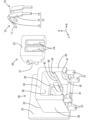
- FIG. 1 is a perspective view of a board connector according to a first embodiment, as viewed obliquely from below and from the front.
- FIG. 2 is a perspective view of the board connector shown in FIG. 1 as viewed obliquely from below and behind.
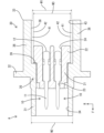
- 3 is an exploded perspective view of the board connector shown in FIG. 1, as viewed obliquely from below and rear. 4 is a side cross-sectional view of the board connector shown in FIG. 1.
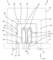
- FIG. FIG. 5 is a plan sectional view of the board connector shown in FIG. 6 is a rear view of the board connector shown in FIG. 1.
- FIG. 1 is a perspective view of a board connector according to a first embodiment, as viewed obliquely from below and from the front.
- FIG. 2 is a perspective view of the board connector shown in FIG. 1 as viewed obliquely from below and behind.
- 3 is an exploded perspective view of the board connector shown in FIG. 1, as viewed obliquely from below and rear.
- the board connector of the present disclosure comprises: (1) An electrical connector includes an inner conductor connected to a circuit board, a dielectric that houses the inner conductor, and an outer conductor that surrounds the dielectric, the outer conductor having a hood that surrounds the front end of the inner conductor and a gate-shaped portion disposed over a range behind the inner conductor and the dielectric, the gate-shaped portion having an opening at a rear surface and a lower surface that faces the circuit board, a rib is formed on the inner surface of at least one of the side walls of the left and right side walls that constitute the gate-shaped portion, and the minimum opposing distance between the pair of side walls including the rib is smaller than the width dimension of the hood portion.
- the minimum opposing distance between the pair of side walls including the rib is smaller than the width dimension of the hood portion, so that the hood portion can be prevented from fitting into the gate-shaped portion.
- the maximum distance between the pair of side walls can be increased, so that impedance matching can be achieved by suppressing a decrease in impedance.
- a storage space that opens to the rear and stores the dielectric is formed in a region of the outer conductor forward of the gate-shaped portion, and that the rib is formed with a guide surface that guides the dielectric during the process of inserting the dielectric into the storage space. This configuration improves the ease of inserting the dielectric into the storage space.
- the board connection portion of the inner conductor connected to the circuit board is exposed on the rear surface of the dielectric in a vertically elongated state, and the rib is disposed only at a height close to the upper or lower end of the board connection portion.
- the board connection portion of the inner conductor connected to the circuit board is exposed on the rear surface of the dielectric in an elongated, vertically extending state, a wide portion having a width greater than the upper and lower ends is formed in an intermediate region of the board connection portion between the upper and lower ends of the board connection portion, and the rib is disposed at a different height in the vertical direction from the wide portion.
- the board connector A of this embodiment 1 has a shielding function and is a connector that is attached to a circuit board P.
- the board connector A is configured by assembling an inner conductor 10, a dielectric 20, and an outer conductor 30.
- the inner conductor 10 is a single part formed by bending a long, thin metal plate.
- the inner conductor 10 has a terminal connection portion 11 that extends in the front-rear direction, and a board connection portion 12 that extends diagonally downward and rearward in a cantilever shape from the rear end of the terminal connection portion 11.
- the board connection portion 12 has an upper end narrow portion 13 that is continuous with the terminal connection portion 11, a lower end narrow portion 14 that is fixed to the circuit board P, and a wide portion 15 that connects the upper end narrow portion 13 and the lower end narrow portion 14.
- the width dimension of the wide portion 15 is larger than the upper end narrow portion 13 and the lower end narrow portion 14.
- the dielectric 20 is a single part made of synthetic resin and has a front storage section 21 and a rear storage section 22.
- the front storage section 21 is formed with a pair of left and right press-in holes 23 that penetrate the front storage section 21 in the front-rear direction.
- the rear storage section 22 is a section that protrudes rearward from the rear end of the front storage section 21.
- the vertical dimension of the rear storage section 22 is larger than the vertical dimension of the front storage section 21.
- the width dimension (horizontal dimension) of the rear storage section 22 is larger than the width dimension of the front storage section 21.
- the rear storage section 22 is formed with a pair of left and right storage grooves 24 that are open rearward and downward. The rear ends of the press-in holes 23 open at the upper ends of the storage grooves 24.
- a pair of left and right inner conductors 10 are attached to the dielectric 20.
- the terminal connection portion 11 is pressed into the press-fit hole 23 from the rear of the dielectric 20.
- the front end of the terminal connection portion 11 protrudes forward from the front accommodating portion 21, and the board connection portion 12 is accommodated in the accommodating groove 24.
- the lower end of the board connection portion 12 protrudes downward from the bottom surface of the dielectric 20 (rear accommodating portion 22).
- the outer conductor 30 is a single metal part formed by die casting. As shown in Figures 1, 2, 4, and 5, the outer conductor 30 has a hood portion 31, a flange portion 32, and a gate-shaped portion 33.
- the shape of the hood portion 31 in a front view of the outer conductor 30 from the front is a rectangle with its long sides facing in the left-right direction.
- the flange portion 32 has a shape that protrudes in the up-down and left-right directions from the rear end portion on the outer circumferential surface of the hood portion 31.
- the gate-shaped portion 33 protrudes rearward from the rear surface of the flange portion 32.
- the gate-shaped portion 33 has an upper wall portion 35, a pair of side wall portions 36, a pair of upper ribs 40, and a pair of lower ribs 41.
- the upper wall portion 35 extends horizontally rearward from the rear surface of the flange portion 32 with its thickness direction facing up and down.
- the left and right side wall portions 36 extend rearward from the rear surface of the flange portion 32 with its thickness direction facing left and right.
- the upper edges of the side wall portions 36 are connected at right angles to the left and right side edges of the upper wall portion 35.
- a pair of legs 37 spaced apart in the front-rear direction are formed on the lower end surface of each side wall portion 36.
- the outer conductor 30 is attached to the circuit board P so as to be conductive by fitting the legs 37 into fitting holes (not shown) in the circuit board P.
- An open space 38 is formed inside the gate-shaped portion 33, which is open to the rear and downward of the gate-shaped portion 33.
- the vertical dimension of the open space 38 is greater than the vertical dimension of the storage space 34.
- the width dimension of the open space 38 is greater than the width dimension of the storage space 34.
- a square stopper 39 is formed on the rear end surface (front end surface) of the open space 38, surrounding the entire opening of the storage space 34.
- the dielectric 20 is attached to the outer conductor 30.
- the dielectric 20 When attaching, the dielectric 20 is inserted into the open space 38 from the rear of the outer conductor 30, the front accommodating portion 21 is fitted into the accommodating space 34, and the rear accommodating portion 22 is placed in the open space 38.
- the front outer peripheral edge of the rear accommodating portion 22 is abutted against the stopper 39, so that the dielectric 20 is positioned in the front-rear direction relative to the outer conductor 30.
- the front end of the terminal connection portion 11 is positioned within the hood portion 31 (within the accommodating space 34).
- the lower end of the board connection portion 12 protrudes downward from the lower surface of the gate-shaped portion 33.
- the maximum opposing distance W1 between the inner faces of the side wall portions 36 is the same as or slightly larger than the width dimension W2 of the hood portion 31 (the distance between the left and right outer faces of the hood portion 31). Therefore, there is a concern that the hood portion 31 may become fitted into the open space 38 when a large number of outer conductors 30 are transported in a bagged or boxed state.
- a pair of upper ribs 40 and a pair of lower ribs 41 are formed on the inner faces of the left and right side wall portions 36, i.e., on the inner wall surfaces where the side wall portions 36 face each other.
- each of the ribs 40, 41 is rectangular.
- One upper rib 40 and one lower rib 41 are formed on each side wall portion 36.
- These ribs 40, 41 extend linearly in the front-rear direction.
- the formation range of the ribs 40, 41 in the front-rear direction is the range from the front end of the open space 38 (stopper 39) to the rear end of the open space 38 (gate-shaped portion 33).
- the upper rib 40 is located in the center of the open space 38 in the height direction. In other words, the upper rib 40 is located within the formation range of the storage space 34 in the up-down direction.
- the lower rib 41 is located lower than the upper rib 40.
- the lower rib 41 is located at the lower end of the open space 38 so as to follow the lower edge of the side wall portion 36.
- the pair of upper ribs 40 are positioned so as to face each other in the left-right direction at the same height.
- the pair of lower ribs 41 are positioned so as to face each other in the left-right direction at the same height.
- the mutually facing inner surfaces of the pair of upper ribs 40 and the mutually facing inner surfaces of the pair of lower ribs 41 are defined as opposing surfaces 42.
- the opposing distance between the opposing surfaces 42 of a pair of upper ribs 40 and the opposing distance between the opposing surfaces 42 of a pair of lower ribs 41 are set to the same dimension.
- This opposing distance is defined as the minimum opposing distance W3 between the left and right side wall portions 36.
- the minimum opposing distance W3 is set to be smaller than the width dimension W2 of the hood portion 31.
- This minimum opposing distance W3 is set to be the same as or slightly larger than the width dimension of the rear housing portion 22 of the dielectric 20 (the distance between the left and right outer surfaces of the rear housing portion 22).
- the rear end of the opposing surface 42 of each rib 40, 41 is formed with a guide surface 43 that is inclined with respect to the length direction of the ribs 40, 41.
- the guide surfaces 43 that face each other in the left-right direction are inclined in a direction that widens the opposing distance toward the rear. If the dielectric 20 is misaligned in the left-right direction relative to the outer conductor 30 when the dielectric 20 is assembled to the outer conductor 30, the outer surface of the front accommodating portion 21 and the outer surface of the rear accommodating portion 22 slide against the guide surface 43, thereby correcting the misalignment of the dielectric 20 relative to the outer conductor 30. As a result, the front accommodating portion 21 is inserted into the accommodating space 34 without getting caught on the stopper 39.
- the board connector A of this embodiment 1 includes an inner conductor 10 connected to a circuit board P, a dielectric 20 that houses the inner conductor 10, and an outer conductor 30 that surrounds the dielectric 20.
- the outer conductor 30 has a hood portion 31 and a gate-shaped portion 33.
- the hood portion 31 surrounds the front end of the terminal connection portion 11 of the inner conductor 10.
- the gate-shaped portion 33 is disposed over a range rearward of the inner conductor 10 and the dielectric 20.
- the gate-shaped portion 33 has an opening at its rear surface and at its lower surface that faces the circuit board P.
- a pair of upper ribs 40 and a pair of lower ribs 41 are formed on the inner surfaces of the left and right side wall portions 36 that constitute the gate-shaped portion 33.
- the minimum opposing distance W3 of the pair of side wall portions 36 including the upper ribs 40 and the lower ribs 41 is smaller than the width dimension W2 of the hood portion 31.
- the minimum opposing distance W3 between the pair of side wall portions 36 including the upper rib 40 and the lower rib 41 is smaller than the width dimension W2 of the hood portion 31, so that the hood portion 31 can be prevented from fitting into the gate-shaped portion 33.
- the maximum opposing distance W1 between the pair of side wall portions 36 can be increased. This prevents a decrease in impedance, and allows impedance matching.
- a storage space 34 for storing the dielectric 20 is formed in the region of the outer conductor 30 forward of the gate-shaped portion 33.
- the storage space 34 opens to the rear.
- the upper rib 40 and the lower rib 41 are formed with guide surfaces 43 that guide the dielectric 20 during the process of inserting the dielectric 20 into the storage space 34. This configuration improves the ease of inserting the dielectric 20 into the storage space 34.
- the board connection portion 12 of the inner conductor 10, which is connected to the circuit board P, is exposed in an elongated shape extending vertically within the accommodation groove 24 on the rear surface of the dielectric 20.
- the upper rib 40 and the lower rib 41 are arranged only at a height close to the upper narrow portion 13 (upper end) and the lower narrow portion 14 (lower end) of the board connection portion 12. This configuration makes it possible to suppress impedance mismatches caused by the formation of the upper rib 40 and the lower rib 41.
- the board connection portion 12 of the inner conductor 10, which is connected to the circuit board P, is exposed in an elongated shape extending vertically in the accommodation groove 24 on the rear surface of the dielectric 20.
- a wide portion 15 having a width greater than both the upper and lower ends (upper narrow portion 13 and lower narrow portion 14) is formed.
- the lower rib 41 is positioned at a different height in the vertical direction from the wide portion 15. With this configuration, it is possible to suppress impedance mismatch caused by the formation of the lower rib 41.
- the present invention is not limited to the embodiments described above and shown in the drawings, but is indicated by the claims.
- the present invention includes the equivalent meaning of the claims and all modifications within the scope of the claims, including the following embodiments.
- the outer conductor is not limited to one made by die casting, but may be one formed by forging or casting, or may be one formed by bending a metal plate.
- the rib may have no guide surface.
- the ribs may be located at a height between the upper and lower ends of the board connection portion.
- the rib may be disposed in a region above the upper end of the board connection portion.
- the ribs may be located at the same height as the wide portion.
- the number of ribs formed on one side wall portion may be one, or may be three or more.
- the rib may be formed on only one of the left and right side wall portions.
- the board connection portion may have a shape in which the wide portion is not formed.
Landscapes
- Details Of Connecting Devices For Male And Female Coupling (AREA)
- Coupling Device And Connection With Printed Circuit (AREA)
Abstract
インピーダンスの整合と、門形部に対する他部材の嵌まり込み防止とを両立させる。 基板用コネクタ(A)は、回路基板(P)に接続される内導体(10)と、内導体(10)を収容する誘電体(20)と、誘電体(20)を包囲する外導体(30)と、を備え、外導体(30)は、内導体(10)の前端部を包囲するフード部(31)と、内導体(10)及び誘電体(20)よりも後方の範囲に亘って配置される門形部(33)と、を有し、門形部(33)は、後面と、回路基板(P)に対向する下面とが開口しており、門形部(33)を構成する左右両側壁部(36)の少なくとも一方の側壁部(36)の内面には、上側リブ(40)と下側リブ(41)が形成され、上側リブ(40)と下側リブ(41)を含む一対の側壁部(36)の最小対向間隔(W3)が、フード部(31)の幅寸法(W2)よりも小さい。
Description
本開示は、基板用コネクタに関するものである。
特許文献1には、外導体を有する基板用コネクタが開示されている。外導体は、下面と後面が開口した門形をなす誘電体包囲部と、誘電体包囲部から前方へ延出した筒部とを有する。誘電体包囲部は、回路基板に固定されている。誘電体包囲部には、内導体を保持した誘電体が収容されている。内導体の基板接続部は、誘電体の後方において誘電体の外部に露出するとともに、誘電体包囲部内に配置されている。誘電体包囲部は、誘電体及び内導体よりも後方に位置する門形部を有する。門形部は、内導体に対するノイズを遮蔽する機能を有する。
門形部は、金属製の部位であるため、インピーダンスが他の領域よりも低くなることがある。この対策としては、門形部を構成する一対の側壁の間隔を広げることによってインピーダンスの整合を図ることが考えられる。しかし、門形部の側壁の間隔を拡げた場合、この間隔が外導体の筒部の幅よりも大きくなると、例えば、多数個の外導体を袋詰め状態で搬送した場合などに、外導体の門形部の中に他の外導体の筒部が嵌り込んでしまう虞がある。
本開示の基板用コネクタは、上記のような事情に基づいて完成されたものであって、インピーダンスの整合と、門形部に対する他部材の嵌まり込み防止とを両立させることを目的とする。
本開示の基板用コネクタは、
回路基板に接続される内導体と、
前記内導体を収容する誘電体と、
前記誘電体を包囲する外導体と、を備え、
前記外導体は、
前記内導体の前端部を包囲するフード部と、
前記内導体及び前記誘電体よりも後方の範囲に亘って配置される門形部と、を有し、
前記門形部は、後面と、前記回路基板に対向する下面とが開口しており、
前記門形部を構成する左右両側壁部の少なくとも一方の前記側壁部の内面には、リブが形成され、
前記リブを含む前記一対の側壁部の最小対向間隔が、前記フード部の幅寸法よりも小さい。
回路基板に接続される内導体と、
前記内導体を収容する誘電体と、
前記誘電体を包囲する外導体と、を備え、
前記外導体は、
前記内導体の前端部を包囲するフード部と、
前記内導体及び前記誘電体よりも後方の範囲に亘って配置される門形部と、を有し、
前記門形部は、後面と、前記回路基板に対向する下面とが開口しており、
前記門形部を構成する左右両側壁部の少なくとも一方の前記側壁部の内面には、リブが形成され、
前記リブを含む前記一対の側壁部の最小対向間隔が、前記フード部の幅寸法よりも小さい。
本開示によれば、インピーダンスの整合と、門形部に対する他部材の嵌まり込み防止とを両立させることができる。
[本開示の実施形態の説明]
最初に本開示の実施形態を列記して説明する。下記の複数の形態例を、矛盾を生じない範囲で任意に組み合わせたものも、発明を実施するための形態に含まれる。
本開示の基板用コネクタは、
(1)回路基板に接続される内導体と、前記内導体を収容する誘電体と、前記誘電体を包囲する外導体と、を備え、前記外導体は、前記内導体の前端部を包囲するフード部と、前記内導体及び前記誘電体よりも後方の範囲に亘って配置される門形部と、を有し、前記門形部は、後面と、前記回路基板に対向する下面とが開口しており、前記門形部を構成する左右両側壁部の少なくとも一方の前記側壁部の内面には、リブが形成され、前記リブを含む前記一対の側壁部の最小対向間隔が、前記フード部の幅寸法よりも小さい。本開示の構成によれば、リブを含む一対の側壁部の最小対向間隔がフード部の幅寸法よりも小さいので、門形部内にフード部が嵌り込むことを抑制できる。リブを形成したことによって、一対の側壁部の最大間隔を拡大することができるので、インピーダンスの低下を抑えることによって、インピーダンスの整合を図ることができる。
最初に本開示の実施形態を列記して説明する。下記の複数の形態例を、矛盾を生じない範囲で任意に組み合わせたものも、発明を実施するための形態に含まれる。
本開示の基板用コネクタは、
(1)回路基板に接続される内導体と、前記内導体を収容する誘電体と、前記誘電体を包囲する外導体と、を備え、前記外導体は、前記内導体の前端部を包囲するフード部と、前記内導体及び前記誘電体よりも後方の範囲に亘って配置される門形部と、を有し、前記門形部は、後面と、前記回路基板に対向する下面とが開口しており、前記門形部を構成する左右両側壁部の少なくとも一方の前記側壁部の内面には、リブが形成され、前記リブを含む前記一対の側壁部の最小対向間隔が、前記フード部の幅寸法よりも小さい。本開示の構成によれば、リブを含む一対の側壁部の最小対向間隔がフード部の幅寸法よりも小さいので、門形部内にフード部が嵌り込むことを抑制できる。リブを形成したことによって、一対の側壁部の最大間隔を拡大することができるので、インピーダンスの低下を抑えることによって、インピーダンスの整合を図ることができる。
(2)(1)において、前記外導体における前記門形部よりも前方の領域には、後方に開口し、前記誘電体を収容する収容空間が形成されており、前記リブには、前記誘電体を前記収容空間に挿入する過程で前記誘電体をガイドするガイド面が形成されていることが好ましい。この構成によれば、誘電体を収容空間に挿入する際の作業性が向上する。
(3)(1)又は(2)において、前記内導体のうち前記回路基板に接続される基板接続部が、前記誘電体の後面において上下方向に細長く延びた状態で露出し、前記リブは、前記基板接続部の上端部又は下端部に近い高さのみに配置されていることが好ましい。この構成によれば、リブの形成に起因するインピーダンスの不整合を抑制することが可能である。即ち、上下方向におけるリブの位置に関して、基板接続部の上端部又は下端部に近い高さとは、基板接続部の上端部又は下端部の近傍でリブによってインピーダンスの低下を招きがたい高さである。
(4)(1)又は(2)において、前記内導体のうち前記回路基板に接続される基板接続部が、前記誘電体の後面において上下方向に細長く延びた状態で露出し、前記基板接続部のうち前記基板接続部の上下両端部の間の中間領域には、前記上下両端部よりも幅寸法の大きい幅広部が形成されており、前記リブが、上下方向において前記幅広部とは異なる高さに配置されていることが好ましい。この構成によれば、リブの形成に起因するインピーダンスの不整合を抑制することが可能である。
[本開示の実施形態の詳細]
[実施例1]
本開示を具体化した実施例1の基板用コネクタAを、図1~図6を参照して説明する。本発明は、これらの例示に限定されるものではなく、請求の範囲によって示され、請求の範囲と均等の意味および範囲内でのすべての変更が含まれる。本実施例1において、前後の方向については、図1~5におけるF方向を前方と定義する。上下の方向については、図1~4,6におけるH方向を上方と定義する。左右の方向については、図1~3,5,6におけるR方向を右方と定義する。左右方向と幅方向を同義で用いる。
[実施例1]
本開示を具体化した実施例1の基板用コネクタAを、図1~図6を参照して説明する。本発明は、これらの例示に限定されるものではなく、請求の範囲によって示され、請求の範囲と均等の意味および範囲内でのすべての変更が含まれる。本実施例1において、前後の方向については、図1~5におけるF方向を前方と定義する。上下の方向については、図1~4,6におけるH方向を上方と定義する。左右の方向については、図1~3,5,6におけるR方向を右方と定義する。左右方向と幅方向を同義で用いる。
本実施例1の基板用コネクタAは、シールド機能を有し、回路基板Pに取り付けられるコネクタである。基板用コネクタAは、図3に示すように、内導体10と、誘電体20と、外導体30とを組み付けて構成されている。内導体10は、金属製の細長い板材に曲げ加工を施して成形された単一部品である。図3,4に示すように、内導体10は、前後方向に延びる端子接続部11と、端子接続部11の後端から斜め下後方へ片持ち状に延出した基板接続部12とを有する。基板接続部12は、端子接続部11に連なる上端側幅狭部13と、回路基板Pに固着される下端側幅狭部14と、上端側幅狭部13と下端側幅狭部14とを繋ぐ幅広部15とを有する。幅広部15の幅寸法は、上端側幅狭部13及び下端側幅狭部14よりも大きい。
誘電体20は、前側収容部21と後側収容部22とを有する合成樹脂製の単一部品である。図4,5に示すように、前側収容部21に、前側収容部21を前後方向に貫通した形態の左右一対の圧入孔23が形成されている。後側収容部22は、前側収容部21の後端部から後方へ突出した部位である。後側収容部22の上下寸法は、前側収容部21の上下寸法よりも大きい。後側収容部22の幅寸法(左右方向の寸法)は、前側収容部21の幅寸法よりも大きい。後側収容部22には、後方及び下方へ開放された左右一対の収容溝24が形成されている。収容溝24の上端部には、圧入孔23の後端が開口している。
誘電体20には、左右一対の内導体10が取り付けられている。取り付けの際には、端子接続部11を、誘電体20の後方から圧入孔23内に圧入する。内導体10を誘電体20に取り付けた状態では、端子接続部11の前端部が前側収容部21から前方へ突出し、基板接続部12が収容溝24内に収容される。基板接続部12の下端部は、誘電体20(後側収容部22)の下面よりも下方へ突出する。
外導体30は、ダイキャストによって成形された金属製の単一部品である。図1,2,4,5に示すように、外導体30は、フード部31と、フランジ部32と、門形部33とを有する。外導体30を前方から視たフード部31の正面視形状は、長辺を左右方向に向けた長方形である。フード部31の内部には、誘電体20の前側収容部21を収容するための収容空間34が形成されている。フランジ部32は、フード部31の外周面における後端部から上下方向及び左右方向へ張り出した形状をなす。
門形部33は、フランジ部32の後面から後方へ突出した形状をなす。門形部33は、上壁部35と、一対の側壁部36と、一対の上側リブ40と、一対の下側リブ41とを有する。上壁部35は、厚さ方向を上下方向に向けて、フランジ部32の後面から後方へ水平に延出している。左右両側壁部36は、厚さ方向を左右方向に向けて、フランジ部32の後面から後方へ延出している。両側壁部36の上端縁は、上壁部35の左右両側縁に対して直角をなして繋がっている。各側壁部36の下端面には、夫々、前後方向に間隔を空けた一対の脚部37が形成されている。外導体30は、脚部37を回路基板Pの嵌合孔(図示省略)に嵌合することによって、回路基板Pに対して導通可能に取り付けられる。
門形部33の内部には、門形部33の後方及び下方に開放された開放空間38が形成されている。開放空間38の上下寸法は、収容空間34の上下寸法よりも大きい。開放空間38の幅寸法は収容空間34の幅寸法よりも大きい。図3~5に示すように、開放空間38と収容空間34の寸法差によって、開放空間38の奥端面(前端面)には、収容空間34の開口を全周に亘って包囲する方形のストッパ39が形成されている。
外導体30には誘電体20が取り付けられている。取り付ける際には、誘電体20を外導体30の後方から開放空間38内に挿入し、前側収容部21を収容空間34内に嵌入するとともに、後側収容部22を開放空間38内に配置する。後側収容部22の前面外周縁部をストッパ39に突き当てることによって、誘電体20が外導体30に対して前後方向に位置決めされる。誘電体20を外導体30に取り付けた状態では、端子接続部11の前端部が、フード部31内(収容空間34内)に配置される。基板接続部12の下端部は、門形部33の下面よりも下方へ突出する。
側壁部36の内面間の最大対向間隔W1(開放空間38の最大幅寸法)は、フード部31の幅寸法W2(フード部31の左右両外側面の間の距離)と同じか、それよりも僅かに大きい寸法である。そのため、多数の外導体30を袋詰め状態や箱詰め状態で運搬した際に、フード部31が開放空間38内に嵌合してしまうことが懸念される。この対策として、左右両側壁部36の内面、即ち、両側壁部36同士が対向する内側壁面には、一対の上側リブ40と一対の下側リブ41が形成されている。
図6に示すように、門形部33を後方から視た背面視において、各リブ40,41は方形をなしている。各側壁部36には、夫々1本の上側リブ40と1本の下側リブ41が形成されている。これらのリブ40,41は、前後方向に直線状に延びている。図5に示すように、前後方向におけるリブ40,41の形成範囲は、開放空間38の前端(ストッパ39)から開放空間38(門形部33)の後端に至る範囲である。
図2~4に示すように、上側リブ40は、開放空間38の高さ方向中央部に配置されている。換言すると、上側リブ40は、上下方向において、収容空間34の形成範囲内に位置している。下側リブ41は、上側リブ40よりも下方に配置されている。下側リブ41は、開放空間38の下端部において、側壁部36の下端縁部に沿うように位置している。一対の上側リブ40は、同じ高さにおいて左右方向に対向するように位置する。一対の下側リブ41は、同じ高さにおいて左右方向に対向するように位置する。一対の上側リブ40の互いに対向する内面、及び一対の下側リブ41の互いに対向する内面を、対向面42と定義する。
一対の上側リブ40における対向面42同士の対向間隔と、一対の下側リブ41における対向面42同士の対向間隔は、同じ寸法に設定されている。この対向間隔を、左右両側壁部36の間の最小対向間隔W3と定義する。最小対向間隔W3は、フード部31の幅寸法W2よりも小さく設定されている。この最小対向間隔W3は、誘電体20の後側収容部22の幅寸法(後側収容部22の左右両外側面の間の距離)と同じか、それよりも僅かに大きい寸法に設定されている。
各リブ40,41の対向面42における後端部には、外導体30を上から視た平面視において、リブ40,41の長さ方向に対して傾斜したガイド面43が形成されている。左右方向に対向するガイド面43同士は、後方に向かって対向間隔を広げる向きに傾斜している。誘電体20を外導体30に組み付ける際に、誘電体20が外導体30に対して左右方向に位置ずれし場合には、前側収容部21の外側面や、後側収容部22の外側面がガイド面43に摺接することによって、外導体30に対する誘電体20の位置ずれが矯正される。これにより、前側収容部21が、ストッパ39に引っ掛かることなく収容空間34内に挿入される。
本実施例1の基板用コネクタAは、回路基板Pに接続される内導体10と、内導体10を収容する誘電体20と、誘電体20を包囲する外導体30と、を備えている。外導体30は、フード部31と門形部33とを有する。フード部31は、内導体10の端子接続部11の前端部を包囲する。門形部33は、内導体10及び誘電体20よりも後方の範囲に亘って配置されている。門形部33は、その後面と、回路基板Pに対向する下面とが開口した形状である。門形部33を構成する左右両側壁部36の内面には、一対の上側リブ40と一対の下側リブ41が形成されている。上側リブ40及び下側リブ41を含む一対の側壁部36の最小対向間隔W3は、フード部31の幅寸法W2よりも小さい。
この構成によれば、上側リブ40と下側リブ41を含む一対の側壁部36の最小対向間隔W3がフード部31の幅寸法W2よりも小さいので、門形部33内にフード部31が嵌り込むことを抑制できる。上側リブ40と下側リブ41を形成したことによって、一対の側壁部36の最大対向間隔W1を拡大することができる。これにより、インピーダンスの低下が抑えられるので、インピーダンスの整合を図ることができる。
外導体30における門形部33よりも前方の領域には、誘電体20を収容するための収容空間34が形成されている。収容空間34は、後方に開口している。上側リブ40と下側リブ41には、誘電体20を収容空間34に挿入する過程で、誘電体20をガイドするガイド面43が形成されている。この構成によれば、誘電体20を収容空間34に挿入する際の作業性が向上する。
内導体10のうち回路基板Pに接続される基板接続部12は、誘電体20の後面の収容溝24内において上下方向に細長く延びた状態で露出している。外導体30を後方から視た背面視において、上側リブ40と下側リブ41は、前記基板接続部12の上端側幅狭部13(上端部)と下端側幅狭部14(下端部)に近い高さのみに配置されている。この構成によれば、上側リブ40と下側リブ41の形成に起因するインピーダンスの不整合を抑制することができる。
内導体10のうち回路基板Pに接続される基板接続部12が、誘電体20の後面の収容溝24内において上下方向に細長く延びた状態で露出している。基板接続部12のうち基板接続部12の上下両端部(上端側幅狭部13と下端側幅狭部14)の間の中間領域には、上下両端部(上端側幅狭部13と下端側幅狭部14)よりも幅寸法の大きい幅広部15が形成されている。上側リブ40と下側リブ41のうち下側リブ41は、上下方向において幅広部15とは異なる高さに配置されている。この構成によれば、下側リブ41の形成に起因するインピーダンスの不整合を抑制することが可能である。
[他の実施例]
本発明は、上記記述及び図面によって説明した実施例に限定されるものではなく、請求の範囲によって示される。本発明には、請求の範囲と均等の意味及び請求の範囲内でのすべての変更が含まれ、下記の実施形態も含まれる。
外導体は、ダイキャスト製のものに限らず、鍛造又は鋳造によって成形されたものでもよく、金属板材を曲げ加工して成形したものでもよい。
リブは、ガイド面を有しない形態でもよい。
リブは、基板接続部の上下両端部の間の高さに配置してもよい。
リブは、基板接続部の上端よりも上方の領域に配置してもよい。
リブは、幅広部と同じ高さに配置してもよい。
1つの側壁部に形成するリブの数は、1つだけでもよく、3つ以上でもよい。
リブは、左右両側側壁部のうちいずれか一方の側壁部のみに形成してもよい。
基板接続部は、幅広部が形成されていない形状でもよい。
本発明は、上記記述及び図面によって説明した実施例に限定されるものではなく、請求の範囲によって示される。本発明には、請求の範囲と均等の意味及び請求の範囲内でのすべての変更が含まれ、下記の実施形態も含まれる。
外導体は、ダイキャスト製のものに限らず、鍛造又は鋳造によって成形されたものでもよく、金属板材を曲げ加工して成形したものでもよい。
リブは、ガイド面を有しない形態でもよい。
リブは、基板接続部の上下両端部の間の高さに配置してもよい。
リブは、基板接続部の上端よりも上方の領域に配置してもよい。
リブは、幅広部と同じ高さに配置してもよい。
1つの側壁部に形成するリブの数は、1つだけでもよく、3つ以上でもよい。
リブは、左右両側側壁部のうちいずれか一方の側壁部のみに形成してもよい。
基板接続部は、幅広部が形成されていない形状でもよい。
A…基板用コネクタ
P…回路基板
W1…側壁部の最大対向間隔
W2…フード部の幅寸法
W3…側壁部の最小対向間隔
10…内導体
11…端子接続部
12…基板接続部
13…上端側幅狭部(上端部)
14…下端側幅狭部(下端部)
15…幅広部
20…誘電体
21…前側収容部
22…後側収容部
23…圧入孔
24…収容溝
30…外導体
31…フード部
32…フランジ部
33…門形部
34…収容空間
35…上壁部
36…側壁部
37…脚部
38…開放空間
39…ストッパ
40…上側リブ(リブ)
41…下側リブ(リブ)
42…対向面
43…ガイド面
P…回路基板
W1…側壁部の最大対向間隔
W2…フード部の幅寸法
W3…側壁部の最小対向間隔
10…内導体
11…端子接続部
12…基板接続部
13…上端側幅狭部(上端部)
14…下端側幅狭部(下端部)
15…幅広部
20…誘電体
21…前側収容部
22…後側収容部
23…圧入孔
24…収容溝
30…外導体
31…フード部
32…フランジ部
33…門形部
34…収容空間
35…上壁部
36…側壁部
37…脚部
38…開放空間
39…ストッパ
40…上側リブ(リブ)
41…下側リブ(リブ)
42…対向面
43…ガイド面
Claims (4)
- 回路基板に接続される内導体と、
前記内導体を収容する誘電体と、
前記誘電体を包囲する外導体と、を備え、
前記外導体は、
前記内導体の前端部を包囲するフード部と、
前記内導体及び前記誘電体よりも後方の範囲に亘って配置される門形部と、を有し、
前記門形部は、後面と、前記回路基板に対向する下面とが開口しており、
前記門形部を構成する左右両側壁部の少なくとも一方の前記側壁部の内面には、リブが形成され、
前記リブを含む前記一対の側壁部の最小対向間隔が、前記フード部の幅寸法よりも小さい基板用コネクタ。 - 前記外導体における前記門形部よりも前方の領域には、後方に開口し、前記誘電体を収容する収容空間が形成されており、
前記リブには、前記誘電体を前記収容空間に挿入する過程で前記誘電体をガイドするガイド面が形成されている請求項1に記載の基板用コネクタ。 - 前記内導体のうち前記回路基板に接続される基板接続部が、前記誘電体の後面において上下方向に細長く延びた状態で露出し、
前記リブは、前記基板接続部の上端部又は下端部に近い高さのみに配置されている請求項1又は請求項2に記載の基板用コネクタ。 - 前記内導体のうち前記回路基板に接続される基板接続部が、前記誘電体の後面において上下方向に細長く延びた状態で露出し、
前記基板接続部のうち前記基板接続部の上下両端部の間の中間領域には、前記上下両端部よりも幅寸法の大きい幅広部が形成されており、
前記リブが、上下方向において前記幅広部とは異なる高さに配置されている請求項1又は請求項2に記載の基板用コネクタ。
Priority Applications (1)
| Application Number | Priority Date | Filing Date | Title |
|---|---|---|---|
| CN202480036786.4A CN121444290A (zh) | 2023-06-07 | 2024-06-04 | 基板用连接器 |
Applications Claiming Priority (2)
| Application Number | Priority Date | Filing Date | Title |
|---|---|---|---|
| JP2023-093874 | 2023-06-07 | ||
| JP2023093874A JP2024175834A (ja) | 2023-06-07 | 2023-06-07 | 基板用コネクタ |
Publications (1)
| Publication Number | Publication Date |
|---|---|
| WO2024253079A1 true WO2024253079A1 (ja) | 2024-12-12 |
Family
ID=93796039
Family Applications (1)
| Application Number | Title | Priority Date | Filing Date |
|---|---|---|---|
| PCT/JP2024/020331 Ceased WO2024253079A1 (ja) | 2023-06-07 | 2024-06-04 | 基板用コネクタ |
Country Status (3)
| Country | Link |
|---|---|
| JP (1) | JP2024175834A (ja) |
| CN (1) | CN121444290A (ja) |
| WO (1) | WO2024253079A1 (ja) |
Citations (1)
| Publication number | Priority date | Publication date | Assignee | Title |
|---|---|---|---|---|
| JP2023018176A (ja) * | 2021-07-27 | 2023-02-08 | 株式会社オートネットワーク技術研究所 | コネクタ |
-
2023
- 2023-06-07 JP JP2023093874A patent/JP2024175834A/ja active Pending
-
2024
- 2024-06-04 WO PCT/JP2024/020331 patent/WO2024253079A1/ja not_active Ceased
- 2024-06-04 CN CN202480036786.4A patent/CN121444290A/zh active Pending
Patent Citations (1)
| Publication number | Priority date | Publication date | Assignee | Title |
|---|---|---|---|---|
| JP2023018176A (ja) * | 2021-07-27 | 2023-02-08 | 株式会社オートネットワーク技術研究所 | コネクタ |
Also Published As
| Publication number | Publication date |
|---|---|
| JP2024175834A (ja) | 2024-12-19 |
| CN121444290A (zh) | 2026-01-30 |
Similar Documents
| Publication | Publication Date | Title |
|---|---|---|
| US7448897B2 (en) | Plug connector with mating protection | |
| JP5582893B2 (ja) | 面実装用マルチコネクタ及び電子機器 | |
| JP6663565B2 (ja) | 基板用コネクタ | |
| US6343951B1 (en) | Electrical connector | |
| CN112385095B (zh) | 屏蔽连接器及外导体端子 | |
| US20150263457A1 (en) | Connector | |
| KR20030052993A (ko) | 실드형 커넥터 | |
| JP7606661B2 (ja) | 基板用コネクタおよび機器 | |
| JP7023499B2 (ja) | 電気コネクタ | |
| CN104078799B (zh) | 中继电连接器 | |
| JP6847016B2 (ja) | 同軸ケーブル用コネクタ | |
| US10700476B2 (en) | Electrical connector | |
| JP5757198B2 (ja) | コネクタ | |
| JP7420009B2 (ja) | コネクタ | |
| JP7609050B2 (ja) | シールドコネクタ | |
| US10971833B2 (en) | Board connector | |
| JP2024175834A (ja) | 基板用コネクタ | |
| JP2024174106A (ja) | シールドコネクタ | |
| JP7569504B2 (ja) | シールドコネクタ | |
| JP4184370B2 (ja) | 電気コネクタ | |
| JP7486536B2 (ja) | シールドコネクタ | |
| JP7851529B2 (ja) | シールドコネクタ | |
| JP7454001B2 (ja) | シールドコネクタ | |
| JP6145531B2 (ja) | 中継電気コネクタ | |
| JP7444908B2 (ja) | シールドコネクタ |
Legal Events
| Date | Code | Title | Description |
|---|---|---|---|
| 121 | Ep: the epo has been informed by wipo that ep was designated in this application |
Ref document number: 24817471 Country of ref document: EP Kind code of ref document: A1 |
|
| WWE | Wipo information: entry into national phase |
Ref document number: CN2024800367864 Country of ref document: CN |
|
| NENP | Non-entry into the national phase |
Ref country code: DE |