WO2024252899A1 - 透明導電性フィルム - Google Patents
透明導電性フィルム Download PDFInfo
- Publication number
- WO2024252899A1 WO2024252899A1 PCT/JP2024/018379 JP2024018379W WO2024252899A1 WO 2024252899 A1 WO2024252899 A1 WO 2024252899A1 JP 2024018379 W JP2024018379 W JP 2024018379W WO 2024252899 A1 WO2024252899 A1 WO 2024252899A1
- Authority
- WO
- WIPO (PCT)
- Prior art keywords
- transparent conductive
- conductive film
- less
- film
- particles
- Prior art date
- Legal status (The legal status is an assumption and is not a legal conclusion. Google has not performed a legal analysis and makes no representation as to the accuracy of the status listed.)
- Ceased
Links
Images


Classifications
-
- B—PERFORMING OPERATIONS; TRANSPORTING
- B32—LAYERED PRODUCTS
- B32B—LAYERED PRODUCTS, i.e. PRODUCTS BUILT-UP OF STRATA OF FLAT OR NON-FLAT, e.g. CELLULAR OR HONEYCOMB, FORM
- B32B7/00—Layered products characterised by the relation between layers; Layered products characterised by the relative orientation of features between layers, or by the relative values of a measurable parameter between layers, i.e. products comprising layers having different physical, chemical or physicochemical properties; Layered products characterised by the interconnection of layers
- B32B7/02—Physical, chemical or physicochemical properties
- B32B7/023—Optical properties
-
- B—PERFORMING OPERATIONS; TRANSPORTING
- B32—LAYERED PRODUCTS
- B32B—LAYERED PRODUCTS, i.e. PRODUCTS BUILT-UP OF STRATA OF FLAT OR NON-FLAT, e.g. CELLULAR OR HONEYCOMB, FORM
- B32B7/00—Layered products characterised by the relation between layers; Layered products characterised by the relative orientation of features between layers, or by the relative values of a measurable parameter between layers, i.e. products comprising layers having different physical, chemical or physicochemical properties; Layered products characterised by the interconnection of layers
- B32B7/02—Physical, chemical or physicochemical properties
- B32B7/025—Electric or magnetic properties
-
- B—PERFORMING OPERATIONS; TRANSPORTING
- B32—LAYERED PRODUCTS
- B32B—LAYERED PRODUCTS, i.e. PRODUCTS BUILT-UP OF STRATA OF FLAT OR NON-FLAT, e.g. CELLULAR OR HONEYCOMB, FORM
- B32B9/00—Layered products comprising a layer of a particular substance not covered by groups B32B11/00 - B32B29/00
-
- H—ELECTRICITY
- H01—ELECTRIC ELEMENTS
- H01B—CABLES; CONDUCTORS; INSULATORS; SELECTION OF MATERIALS FOR THEIR CONDUCTIVE, INSULATING OR DIELECTRIC PROPERTIES
- H01B5/00—Non-insulated conductors or conductive bodies characterised by their form
- H01B5/14—Non-insulated conductors or conductive bodies characterised by their form comprising conductive layers or films on insulating-supports
Definitions
- the present invention relates to a transparent conductive film in which a transparent conductive film of indium-tin composite oxide is laminated onto a transparent plastic film substrate.
- Transparent conductive films which are made by laminating a transparent, low-resistance thin film onto a transparent plastic film substrate, are widely used in electrical and electronic applications that utilize their electrical conductivity, such as in flat panel displays such as liquid crystal displays and electroluminescence (EL) displays, and as transparent electrodes in touch panels.
- flat panel displays such as liquid crystal displays and electroluminescence (EL) displays
- EL electroluminescence
- a resistive touch panel combines a fixed electrode made of a glass or plastic substrate coated with a transparent conductive thin film with a movable electrode (called a film electrode) made of a plastic film coated with a transparent conductive thin film, and is used by overlapping it on top of the display.
- a film electrode a movable electrode
- the film electrode is pressed with a finger or pen (called input)
- the transparent conductive thin film of the fixed electrode and the film electrode come into contact with each other, and the input position is recognized.
- Patent Document 1 discloses a transparent conductive film in which a transparent conductive thin film made of an indium-tin composite oxide or a tin-antimony composite oxide is laminated on a plastic film, the transparent conductive thin film surface having a center line average roughness (Ra) of 0.1 to 0.5 ⁇ m.
- Patent Document 2 discloses a transparent conductive film including a support and a transparent conductive layer formed on one surface of the support, the surface on the transparent conductive layer side having a surface roughness Ra1 of 7 to 20 nm and the number of protrusions having a height of 250 nm or more being less than 140/ mm2 .
- resistive touch panels must be able to continue inputting even when touched lightly after inputting with a relatively strong force using a pen or finger (continuous input durability). It is also important for resistive touch panels to prevent the fixed electrode and film electrode from sticking together (anti-sticking). Furthermore, because the transparent conductive film is located on the outermost layer of a resistive touch panel, it must have a good appearance (clear, not whitish, and uniform across the entire surface without any unevenness).
- the transparent conductive film described in Patent Document 2 has good durability to continuous input and good appearance, but does not have satisfactory anti-sticking properties.
- the object of the present invention is therefore to provide a transparent conductive film that is excellent in all respects: durability against continuous input, anti-sticking properties, and appearance.
- a transparent conductive film comprising a transparent plastic film substrate and a transparent conductive film of an indium-tin composite oxide laminated on at least one surface of the substrate, the transparent conductive film has an average arithmetic mean height (AVSa) of 2 nm or more and 50 nm or less; the average maximum peak height (AVSp) of the transparent conductive film is 150 nm or more and 1000 nm or less; the average protrusion width on the transparent conductive film side surface and on the surface opposite to the surface on which the transparent conductive film is laminated, determined by the following Test Method 1, is 12 ⁇ m or less; A transparent conductive film, wherein the laminate strength of the transparent conductive film determined by the following Test Method 2 is 450 N/15 mm or more.
- Test method 1 Particle analysis is performed using a three-dimensional surface shape measuring device, Vertscan (measurement conditions: wave mode, measurement wavelength 560 nm, objective lens 50x, field of view 188.709 ⁇ m ⁇ 141.496 ⁇ m) in the following steps (i) to (v). (i) The cross-sectional area ( Tc ) of all protrusions at a height of 0.1 ⁇ m from the lowest point on the measurement surface is determined.
- Average protrusion width (B) 2 x (A ⁇ ) 0.5
- Test method 2 A urethane-based two-liquid curing adhesive (containing 4% by mass of ethyl acetate as a solvent) is applied to the transparent conductive film side surface of the transparent conductive film using a wire bar #5, and then heated at 60° C. for 1 minute.
- the adhesive-coated surface of the transparent conductive film and the PET surface of a PET film are then laminated at 60° C. by a dry lamination method (0.3 MPa, width 70 cm), and aged at 40° C. for 4 days to obtain a laminate for evaluation.
- the obtained laminate is cut into a width of 15 mm and a length of 150 mm to obtain a test piece, and a T-peel test is performed under conditions of a temperature of 23° C., a relative humidity of 65%, and a peel speed of 100 mm/min to measure the maximum load.
- the transparent conductive film has a thickness of 10 nm or more and 100 nm or less, The transparent conductive film has a tin oxide concentration of 0.5% by mass or more and 11% by mass or less, The static friction coefficient of the transparent conductive film is 1.00 or less, The transparent conductive film according to [1], wherein the transparent conductive film has a dynamic friction coefficient of 0.80 or less.
- a curable resin layer is provided between the transparent plastic film substrate and the transparent conductive film, The transparent conductive film according to any one of [1] to [3], which has a functional layer on the opposite side of the transparent plastic film substrate to the side on which the transparent conductive film is present.
- the curable resin layer contains at least one type of particles selected from inorganic particles and organic particles.
- an easy-adhesion layer is disposed between the transparent plastic film substrate and the curable resin layer, or between the transparent plastic film substrate and the functional layer, or both.
- the present invention provides a transparent conductive film that is excellent in all respects: durability against continuous input, anti-sticking properties, and appearance.
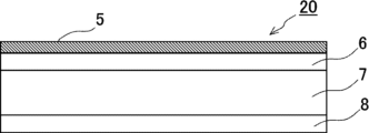
- FIG. 1 is a schematic side view showing an example of the transparent conductive film of the present invention.
- FIG. 2 is a schematic side view showing another example of the transparent conductive film of the present invention.
- FIG. 3 is a schematic side view showing another example of the transparent conductive film of the present invention.
- FIG. 4 is a schematic side view showing another example of the transparent conductive film of the present invention.
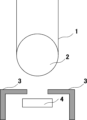
- FIG. 5 is a schematic diagram of an apparatus showing an example of the film forming method of the present invention.
- the transparent conductive film 20 of the present invention has a structure in which a transparent conductive film 5 is laminated on at least one surface of a transparent plastic film substrate 7.
- the transparent conductive film 20 has a transparent conductive film 5 on its surface
- the transparent conductive film according to the present invention can be widely used in applications that utilize its conductivity, such as flat panel displays such as liquid crystal displays and electroluminescence (EL) displays, and transparent electrodes for touch panels, in electrical and electronic applications.
- flat panel displays such as liquid crystal displays and electroluminescence (EL) displays
- EL electroluminescence
- the transparent conductive film 20 of the present invention preferably has a curable resin layer 6 between the transparent plastic film substrate 7 and the transparent conductive film 5.
- the curable resin layer 6 plays the role of a base layer for the transparent conductive film 5, and the curable resin layer 6 can block monomers and oligomers generated from the transparent plastic film substrate 7 from precipitating on the transparent conductive film 5. This improves the appearance of the transparent conductive film 20.
- the curable resin layer 6 it is possible to improve durability against continuous input and sticking resistance.
- the transparent conductive film 20 of the present invention preferably has a functional layer 8 on the side of the transparent plastic film substrate 7 opposite to the side on which the transparent conductive film 5 is present.
- the functional layer 8 can easily impart properties such as a good appearance, smooth input properties that do not catch fingers, and resistance to scratches when inputting with a pen or the like to the transparent conductive film 20.
- the ability to prevent scratches when inputting is preferably 2H or more when the pencil hardness is measured in accordance with JIS K5600-5-4:1999.
- the curable resin layer 6 and/or the functional layer 8 are not necessarily required, but providing these layers can improve durability against continuous input, sticking resistance, appearance, etc. Also, by appropriately changing the configuration of the curable resin layer 6 and the functional layer 8 (for example, the number-average particle size and content of the particles optionally contained, the content of the leveling agent, the thickness of each layer, etc.), it is possible to adjust the AVSa, AVSp, average protrusion width, and laminate strength of the transparent conductive film.
- the transparent conductive film 20 of the present invention preferably has an easy-adhesion layer (e.g., 9A, 9B) on at least one side of the transparent plastic film substrate 7.
- the easy-adhesion layers (9A, 9B) serve to firmly adhere the transparent plastic film substrate 7 to the cured resin layer 6, or the transparent plastic film substrate 7 to the functional layer 8. This strong adhesion can improve the durability against continuous input and prevent damage to the functional layer.
- a layer such as the easy-adhesion layer 9A between the transparent plastic film substrate 7 and the cured resin layer 6, the force acting in the thickness direction on the transparent conductive film 5 can be dispersed, thereby preventing cracking, peeling, wear, etc., of the transparent conductive film during the continuous input durability test.
- the easy-adhesion layer is disposed between the transparent plastic film substrate 7 and the curable resin layer 6 or between the transparent plastic film substrate 7 and the functional layer 8, or both.
- the transparent conductive film 20 in FIG. 2 has a structure in which the transparent plastic film substrate 7 and the curable resin layer 6 are laminated (adhered) via an easy-adhesion layer 9A.
- the transparent conductive film 20 in FIG. 3 has a structure in which the transparent plastic film substrate 7 and the functional layer 8 are laminated (adhered) via an easy-adhesion layer 9B.
- the 4 has a structure in which the transparent plastic film substrate 7 and the curable resin layer 6 are laminated (adhered) via an easy-adhesion layer 9A, and the transparent plastic film substrate 7 and the functional layer 8 are laminated (adhered) via an easy-adhesion layer 9B.
- the easy-adhesion layer may or may not be in direct contact with each of the transparent plastic film substrate 7, the curable resin layer 6, and the functional layer 8.
- the total light transmittance of the transparent conductive film is preferably 70% or more and 95% or less, more preferably 80% or more and 93% or less, and even more preferably 85% or more and 90% or less.
- the continuous input durability of the transparent conductive film is preferably 7,500 times or more, more preferably 15,000 times or more, and even more preferably 3,000 times or more. The higher the value of the continuous input durability, the better, and there is no particular upper limit.
- the transparent conductive film of the present invention has excellent anti-sticking properties, so in resistive touch panels, it can prevent the fixed electrode and film electrode from sticking together (sticking) when the film electrode is pressed and slid with a finger, pen, etc. This allows for precise control of the touch panel input position.
- the transparent conductive film of the present invention is uniform across its entire surface, without unevenness. Furthermore, the average value of the transmitted image clarity of the transparent conductive film is approximately 460-500% (preferably approximately 470-500%; the higher the value, the less whitish it is, which is preferable), so the transparent conductive film is clear and not whitish.
- the method for measuring the average transmitted image clarity is described in detail in the Examples section.
- the average arithmetic mean height (AVSa) of the transparent conductive film is 2 nm or more and 50 nm or less, preferably 3 nm or more and 30 nm or less, more preferably 4 nm or more and 15 nm or less.
- AVSa average arithmetic mean height
- the transparent conductive film has good continuous input durability, anti-sticking property and appearance.
- AVSa is large, the anti-sticking property tends to improve, and when AVSa is small, the continuous input durability tends to improve.
- AVSa is small, the whitishness of the entire transparent conductive film tends to decrease and the appearance tends to improve.
- AVSa has a particularly strong influence on anti-sticking property and appearance.
- AVSa is set to the above range from the balance between anti-sticking property and appearance.
- the average maximum peak height (AVSp) of the transparent conductive film is 150 nm or more and 1000 nm or less, preferably 200 nm or more and 800 nm or less, and more preferably 250 nm or more and 600 nm or less.
- AVSp average maximum peak height
- AVSp is set to the above range.
- the transparent conductive film of the present invention has an average protrusion width of 12 ⁇ m or less on the transparent conductive film side surface and the surface opposite to the surface on which the transparent conductive film is laminated, as determined by the following test method 1.
- the average protrusion width is within the above range, white spots caused by protrusions on the transparent conductive film surface become very difficult to see, and the appearance is improved.
- the smaller the average protrusion width the less likely the white spots caused by protrusions on the transparent conductive film surface become to be seen, and the appearance tends to improve.
- the average protrusion width is preferably 0.01 ⁇ m or more and 11 ⁇ m or less, more preferably 0.03 ⁇ m or more and 10 ⁇ m or less, and even more preferably 0.05 ⁇ m or more and 9 ⁇ m or less.
- Test method 1 Particle analysis is performed using a three-dimensional surface shape measuring device, Vertscan (measurement conditions: wave mode, measurement wavelength 560 nm, objective lens 50x, field of view 188.709 ⁇ m ⁇ 141.496 ⁇ m) in the following steps (i) to (v). (i) The cross-sectional area ( Tc ) of all protrusions at a height of 0.1 ⁇ m from the lowest point on the measurement surface is determined.
- the transparent conductive film of the present invention has a laminate strength of 450N/15mm or more as determined by the following test method 2.
- the laminate strength of the transparent conductive film is within the above range, the transparent conductive film can be evaluated as having high adhesion to its lower layer, and the transparent conductive film is less likely to peel off, so that the continuous input durability can be improved.
- a higher laminate strength is desirable for continuous input durability, and the laminate strength is preferably 500N/15mm or more, more preferably 550N/15mm or more.
- the laminate strength is preferably 500N/15mm or more, more preferably 550N/15mm or more.
- the laminate strength is too high, the adhesive layer may be destroyed during measurement, and the laminate strength may not be measured accurately.
- the laminate strength is generally 2000N/15mm or less, and may be 1500N/15mm or less, 1000N/15mm or less, or 800N/15mm or less. That is, the laminate strength of the transparent conductive film determined by the following Test Method 2 is preferably 500 to 2000 N/15 mm, more preferably 500 to 1500 N/15 mm, even more preferably 550 to 1000 N/15 mm, and even more preferably 550 to 800 N/15 mm. Note that the following Test Method 2 can adequately determine high adhesion of the transparent conductive film compared to an adhesion test conforming to JIS K5600-5-6:1999, which is known as a general adhesion evaluation method, and therefore can be said to be a test more suitable for evaluating the transparent conductive film that contributes to continuous input durability.
- Test method 2 A urethane-based two-liquid curing adhesive (containing 4% by mass of ethyl acetate as a solvent) is applied to the transparent conductive film side surface of the transparent conductive film using a wire bar #5, and then heated at 60° C. for 1 minute. The adhesive-coated surface of the transparent conductive film and the PET surface of a PET film (thickness 100 ⁇ m) are then laminated at 60° C. by a dry lamination method (0.3 MPa, width 70 cm), and aged at 40° C. for 4 days to obtain a laminate for evaluation.
- a dry lamination method 0.3 MPa, width 70 cm
- the obtained laminate is cut into a width of 15 mm and a length of 150 mm to obtain a test piece, and a T-peel test is performed under conditions of a temperature of 23° C., a relative humidity of 65%, and a peel speed of 100 mm/min to measure the maximum load.
- the thickness of the transparent conductive film is preferably 10 nm to 100 nm, more preferably 13 nm to 50 nm, even more preferably 15 nm to 30 nm, and even more preferably 16 nm to 25 nm. If the thickness of the transparent conductive film is 10 nm or more, the entire transparent conductive film adheres to the entire transparent plastic film substrate (or the cured resin layer if a cured resin layer is laminated), stabilizing the film quality of the transparent conductive film and leading to a stable surface resistance value. It is also effective in increasing the laminate strength of the transparent conductive film.
- the thickness of the transparent conductive film is 100 nm or less, the reflection and absorption of light by the transparent conductive film is appropriate, and the total light transmittance is at a practical level. It is also preferable from the viewpoint of productivity.
- the tin oxide concentration contained in the transparent conductive film is preferably 0.5% by mass or more and 11% by mass or less, more preferably 1% by mass or more and 8% by mass or less, and even more preferably 2% by mass or more and 6% by mass or less.
- the tin oxide concentration contained in the transparent conductive film is preferably 0.5% by mass or more and 11% by mass or less, more preferably 1% by mass or more and 8% by mass or less, and even more preferably 2% by mass or more and 6% by mass or less.
- the surface resistance of the transparent conductive film becomes at a practical level, which is preferable.
- the transparent conductive film becomes more likely to crystallize, and the durability to continuous input and total light transmittance can be improved.
- being within the above range is also effective in increasing the laminate strength of the transparent conductive film.
- the crystallinity of the transparent conductive film is preferably 70% or more, more preferably 80% or more, and even more preferably 90% or more. If the crystallinity of the transparent conductive film is 70% or more, the abrasion resistance and laminate strength of the transparent conductive film will be high, leading to improved durability against continuous input. Furthermore, if it is within the above range, the transparency of the transparent conductive film will be high, and the total light transmittance can be improved. The higher the crystallinity, the more preferable it is, with the upper limit being 100% or less.
- the static friction coefficient of the transparent conductive film is preferably 1.00 or less, more preferably 0.80 or less, and even more preferably 0.50 or less. Within this range, the transparent conductive film slides well with the fixed electrode, improving anti-sticking properties. The smaller the static friction coefficient of the transparent conductive film, the better, and considering low-cost production, it is usually 0.15 or more.
- the dynamic friction coefficient of the transparent conductive film is preferably 0.80 or less, more preferably 0.60 or less, and even more preferably 0.50 or less. Within this range, the transparent conductive film slides well with the fixed electrode, improving anti-sticking properties. The smaller the dynamic friction coefficient of the transparent conductive film, the better, and considering low-cost production, it is usually 0.15 or more.
- the surface resistance of the transparent conductive film is preferably 50 ⁇ / ⁇ or more and 900 ⁇ / ⁇ or less, more preferably 60 ⁇ / ⁇ or more and 700 ⁇ / ⁇ or less, and even more preferably 70 ⁇ / ⁇ or more and 500 ⁇ / ⁇ or less. If the surface resistance is within the above range, it will be a transparent conductive film of a practical standard.
- the method for forming the transparent conductive film is not particularly limited, but a preferred method is, for example, to form a transparent conductive film of indium-tin composite oxide by sputtering on at least one surface of a transparent plastic film substrate 7 (hereinafter referred to as the film to be treated), on whose surface a cured resin layer 6 may be formed.
- a so-called roll-type sputtering device which supplies the film to be treated from a film roll, and winds it up into the shape of a film roll after film formation.
- FIG. 5 is a schematic diagram of an example of a film formation method in a roll-type sputtering device.
- the film 1 to be treated fed from a film roll (not shown), runs while partially contacting the surface of the center roll 2.
- An indium-tin sputtering target 4 is placed in a chimney 3 with an opening toward the contact point between the film 1 to be treated and the center roll 2, and a thin film of indium-tin composite oxide is deposited and laminated on the surface of the film 1 to be treated running on the center roll 2.
- the temperature of the center roll 2 can be controlled by a temperature regulator (not shown).
- the target it is preferable to use a sintered target of indium-tin composite oxide.
- a sintered target of indium-tin composite oxide may be placed in the direction of film flow.
- oxygen gas such as argon gas
- inert gas such as argon gas
- the flow rate ratio (volume ratio) of oxygen gas to inert gas is, for example, 0.005 or more, preferably 0.010 or more, more preferably 0.020 or more, and, for example, 0.15 or less, preferably 0.1 or less, more preferably 0.07 or less, and even more preferably 0.05 or less.
- a hydrogen atom-containing gas (hydrogen, ammonia, a hydrogen + argon mixed gas, or the like, so long as it contains hydrogen atoms, but excluding water) may be flowed into the film formation atmosphere using a mass flow controller as necessary.
- the median value (the intermediate value between the maximum value and the minimum value) of the ratio of the water pressure to the inert gas in the film formation atmosphere is, for example, 7.00 ⁇ 10 ⁇ 3 or less, preferably 5.00 ⁇ 10 ⁇ 3 or less, and more preferably 3.00 ⁇ 10 ⁇ 3 or less.
- it is possible to control the water content using the ultimate vacuum as a guide it is preferable to measure the water content (water pressure) during film formation for the following two reasons.
- the film when a film is formed on a plastic film by sputtering, the film is heated and water is released from the film. The ultimate vacuum does not reflect the influence of this released water amount. Second, the ultimate vacuum does not reflect the influence of the water at the center of the roll when a film is formed on a film unwound from the film roll.
- a film roll is held in a vacuum chamber, water is easily removed from the outer layer part of the roll, but water is difficult to remove from the inner layer part of the roll.
- the median value of the moisture pressure ratio may be 0.3 ⁇ 10
- the film roll for forming a transparent conductive film preferably has a height difference between the most convex and most concave points on the roll end face of 10 mm or less, more preferably 8 mm or less, and even more preferably 4 mm or less. If it is 10 mm or less, water and organic components are less likely to be released from the film end face when the film roll is placed in a sputtering device, resulting in good film quality of the transparent conductive film.
- the height difference may be 1 mm or more.
- the bombardment process involves applying a voltage to discharge and generate plasma while flowing only an inert gas such as argon gas, or a mixture of a reactive gas such as oxygen and an inert gas. Specifically, it is desirable to bombard the film by RF sputtering using a SUS target or the like.
- the bombardment process exposes the film to plasma, which releases water and organic components from the film, reducing the amount of water and organic components released from the film when the transparent conductive film is formed, improving the quality of the transparent conductive film.
- the bombardment process activates the layer that the transparent conductive film comes into contact with, improving the adhesion (lamination strength) of the transparent conductive film and further improving its durability against continuous input.
- the treated film 1 may have a protective film with low water absorption attached to the surface opposite the surface on which the transparent conductive film is formed. By attaching the protective film, gases such as water are less likely to be released from the treated film 1, improving the quality of the transparent conductive film.
- the base material for the protective film include olefins such as polyethylene, polypropylene, and cycloolefin.
- the film 1 to be treated is cooled, for example, to below 0°C, preferably below -5°C.
- the film temperature during film formation can be substituted with the set temperature of a temperature regulator that adjusts the temperature of the center roll with which the running film comes into contact (when there are multiple set temperatures, the intermediate value between the maximum and minimum values).
- the film temperature may be -20°C or higher.
- the sputtering apparatus is preferably equipped with an exhaust device such as a rotary pump, turbomolecular pump, or cryopump.
- an exhaust device such as a rotary pump, turbomolecular pump, or cryopump.
- the amount of moisture in the film formation atmosphere can be controlled by the exhaust device.
- the temperature is preferably 100°C to 180°C, more preferably 120°C to 170°C.
- the time is preferably 0.3 to 6 hours, more preferably 0.5 to 2 hours.
- the transparent plastic film substrate is a film obtained by melt-extruding or solution-extruding an organic polymer into a film shape, and then stretching the film in the longitudinal direction and/or the transverse direction, cooling, and heat setting as necessary.
- the transparent plastic film substrate may be a uniaxially oriented film or a biaxially oriented film.
- the organic polymers include polyolefins such as polyethylene and polypropylene; polyesters such as polyethylene terephthalate, polyethylene-2,6-naphthalate, polypropylene terephthalate, and polybutylene terephthalate; polyamides such as nylon 6, nylon 4, nylon 66, and nylon 12; polyimide, polyamideimide, polyethersulfane, polyetheretherketone, polycarbonate, polyarylate, cellulose propionate, polyvinyl chloride, polyvinylidene chloride, polyvinyl alcohol, polyetherimide, polyphenylene sulfide, polyphenylene oxide, polystyrene, syndiotactic polystyrene, and norbornene-based polymers.
- polyolefins such as polyethylene and polypropylene
- polyesters such as polyethylene terephthalate, polyethylene-2,6-naphthalate, polypropylene terephthalate, and polybutylene terephthalate
- polyethylene terephthalate polypropylene terephthalate, polybutylene terephthalate, polyethylene-2,6-naphthalate, syndiotactic polystyrene, norbornene-based polymers, polycarbonate, and polyarylate are preferred.
- These organic polymers may be copolymerized with small amounts of monomers of other organic polymers, or may be blended with other organic polymers.
- the transparent plastic film substrate may be subjected to a surface activation treatment such as corona discharge treatment, glow discharge treatment, flame treatment, ultraviolet irradiation treatment, electron beam irradiation treatment, or ozone treatment, as long as it does not impair the object of the present invention.
- a surface activation treatment such as corona discharge treatment, glow discharge treatment, flame treatment, ultraviolet irradiation treatment, electron beam irradiation treatment, or ozone treatment, as long as it does not impair the object of the present invention.
- the thickness of the transparent plastic film substrate is preferably 80 ⁇ m or more and 240 ⁇ m or less, more preferably 120 ⁇ m or more and 220 ⁇ m or less.
- the thinner the substrate the longer the length of the film that can be introduced into a device for depositing a transparent conductive film, such as a roll-type sputtering device, and this is preferable from the standpoint of productivity.
- the substrate is 80 ⁇ m or more thick, mechanical strength is maintained, so that deformation due to input with a pen or the like is small when used in a touch panel, and durability to continuous input is excellent, which is preferable.
- the thickness is 240 ⁇ m or less, it is preferable because input can be made with light force when used in a touch panel.
- the resin constituting the curable resin layer may be any resin that is cured by application of energy such as heating, ultraviolet light irradiation, or electron beam irradiation, or by a curing agent.
- the resin include silicone-based resins, (meth)acrylic-based resins, epoxy-based resins, Examples of the resin include melamine-based resins, polyester-based resins, and urethane-based resins. These may be used alone or in combination of two or more.
- the resin to be applied is preferably an ultraviolet-curable resin.
- ultraviolet-curable resins examples include polyfunctional (meth)acrylate resins such as acrylic acid esters or methacrylic acid esters of polyhydric alcohols; polyfunctional urethane (meth)acrylate resins such as those synthesized from diisocyanates, polyhydric alcohols, and hydroxyalkyl esters of acrylic acid or methacrylic acid; and the like. These polyfunctional resins may be copolymerized with monofunctional monomers such as vinylpyrrolidone, methyl methacrylate, and styrene, as necessary.
- the curable resin layer may contain, in addition to the resin constituting the curable resin layer described above (i.e., the resin that is the main component constituting the curable resin layer), a resin that is not compatible with the resin described above (hereinafter, may be simply referred to as an incompatible resin).
- an incompatible resin By dispersing the incompatible resin in the curable resin layer, it is possible to form appropriate unevenness on the surface of the curable resin layer, and to increase the surface roughness over a wide area.
- incompatible resins include polyester-based resins, polyolefin-based resins, polystyrene-based resins, and polyamide-based resins.
- the curable resin layer preferably further contains particles.
- the particles can form appropriate unevenness on the surface of the curable resin layer and the transparent conductive film adjacent thereto. This means that the AVSa and AVSp of the transparent conductive film can be controlled within a predetermined range.
- unevenness is formed on the transparent conductive film due to the unevenness of the surface of the curable resin layer.
- a resistive touch panel when the transparent conductive film and the fixed electrode come into contact with each other, a gap is formed between the fixed electrode and the transparent conductive film due to the unevenness of the transparent conductive film, which suppresses adhesion (sticking) between the transparent conductive film and the fixed electrode. Since sticking can cause the touch panel to malfunction, it is essential in this field to prevent sticking.
- the curable resin layer contains particles, it is also possible to improve the durability against continuous input, anti-Newton ring properties, and film winding properties.
- the particles contained in the curable resin layer include at least one type selected from inorganic particles and organic particles.
- inorganic particles include silica particles.
- organic particles include particles made of polyester resin, polyolefin resin, polystyrene resin, polyamide resin, acrylic resin, etc. These may be used alone or in combination of two or more types.
- the particles may be either monodisperse or polydisperse, with monodisperse being preferred.
- a preferred embodiment of the curable resin layer includes particles (A) having a number average particle diameter of 1.0 ⁇ m or more and 6.5 ⁇ m or less. Another preferred embodiment of the curable resin layer includes particles (B) having a number average particle diameter of 0.01 ⁇ m or more and less than 1.0 ⁇ m. Another preferred embodiment of the curable resin layer includes particles (A) having a number average particle diameter of 1.0 ⁇ m or more and 6.5 ⁇ m or less, and particles (B) having a number average particle diameter of 0.01 ⁇ m or more and less than 1.0 ⁇ m. Each of the particles (A) and the particles (B) may be used alone or in combination of two or more kinds.
- the number average particle diameter of the particles (A) is more preferably 2.0 ⁇ m or more and 5.5 ⁇ m or less, and even more preferably 2.8 ⁇ m or more and 5.0 ⁇ m or less.
- the number average particle diameter of the particles (B) is more preferably 0.06 ⁇ m or more and 0.5 ⁇ m or less, and even more preferably 0.1 ⁇ m or more and 0.4 ⁇ m or less. If the number average particle diameter is large, the unevenness of the transparent conductive film becomes large, and as a result, the AVSa and AVSp of the transparent conductive film become large, and the sticking resistance improves.
- the number average particle diameter is small, the unevenness of the transparent conductive film becomes small, and as a result, the AVSa and AVSp of the transparent conductive film become small, and the continuous input durability improves.
- the average protrusion width tends to become small. As a result, the whitishness of the entire surface of the curable resin layer disappears, and the white spots caused by the protrusions of the curable resin layer become less visible, resulting in a good appearance.
- the standard deviation of the particle diameters of particles (A) and particles (B) is preferably 20% or less of the number average particle diameter, more preferably 10% or less of the number average particle diameter, and even more preferably 5% or less of the number average particle diameter.
- the smaller the standard deviation of the particle diameters the more uniform the height of the irregularities in the curable resin layer, thereby achieving stable anti-sticking properties and durability to continuous input. Furthermore, uniformity in the height of the irregularities in the curable resin layer reduces the frequency of white spots caused by protrusions on the curable resin layer, resulting in a good appearance.
- the number-average particle diameter of the particles (A) is preferably slightly smaller than or equal to the thickness of the curable resin layer. By adjusting the balance between the number-average particle diameter of the particles (A) and the thickness of the curable resin layer, it is easy to control AVSa and AVSp.
- the number-average particle diameter of the particles (A) is preferably 0.7 to 1.5 times the thickness of the curable resin layer, more preferably 0.8 to 1.4 times, and even more preferably 0.9 to 1.3 times. If it is 0.7 times or more, it becomes easier to form appropriate unevenness in the curable resin layer, and the winding property of the film is also improved. If it is 1.5 times or less, the falling off of the particles can be suppressed even when a strong load is applied.
- AVSa, AVSp, and the average protrusion width may become too large.
- AVSa, AVSp, and the average projection width can be reduced by reducing the number average particle diameter of the particles (A) or by reducing the amount of particles (A) added.
- AVSa and AVSp can be increased by increasing the number average particle diameter of the particles (A), etc.
- the particles (A) are preferably contained in an amount of 0.1% by mass to 30% by mass, more preferably 2.5% by mass to 20% by mass, and even more preferably 5% by mass to 15% by mass, based on 100% by mass of the solid content constituting the curable resin layer.
- the particles (B) are preferably contained in an amount of 0.05% by mass to 25% by mass, more preferably 0.1% by mass to 22% by mass, and even more preferably 0.5% by mass to 18% by mass, based on 100% by mass of the solid content constituting the curable resin layer.
- the content of particles (B) is preferably 0.1 mass% or more and 99.9 mass% or less, more preferably 20 mass% or more and 80 mass% or less, and even more preferably 30 mass% or more and 70 mass% or less.
- Particles (A) may be either inorganic or organic particles, but are preferably organic particles, and more preferably particles made of acrylic resin.
- Particles (B) may be either inorganic or organic particles, but are preferably inorganic particles, and more preferably silica particles.
- the thickness of the curable resin layer is preferably 0.8 ⁇ m to 6.2 ⁇ m, more preferably 1.0 ⁇ m to 5.0 ⁇ m, and even more preferably 2.0 ⁇ m to 4.0 ⁇ m. If the thickness of the curable resin layer is 0.8 ⁇ m or more, even if the curable resin layer contains particles, sufficient protrusions can be formed while preventing the particles from falling off. On the other hand, if the thickness of the curable resin layer is 6.2 ⁇ m or less, productivity is good. Note that if the curable resin layer is thick, AVSa, AVSp, and average protrusion width tend to decrease.
- the curable resin layer is formed by preparing a liquid composition for a curable resin layer that contains a resin capable of forming a curable resin layer, applying the composition for a curable resin layer to an object to be laminated (e.g., a transparent plastic film substrate, an easy-adhesion layer, etc.), and then curing the resin.
- a resin capable of forming a curable resin layer e.g., a transparent plastic film substrate, an easy-adhesion layer, etc.
- composition for the curable resin layer may contain, in addition to the resin capable of forming the curable resin layer described above, further incompatible resins, particles, curing reaction initiators, solvents, various known additives, etc.
- the curing reaction initiator can be selected according to the type of curing of the resin that constitutes the curable resin layer, and examples of such initiators include thermal polymerization initiators, radical polymerization initiators such as photopolymerization initiators, and various curing agents, among which photopolymerization initiators are preferred.
- thermal polymerization initiators such as thermal polymerization initiators
- radical polymerization initiators such as photopolymerization initiators
- various curing agents among which photopolymerization initiators are preferred.
- photopolymerization initiator known initiators that absorb ultraviolet light and generate radicals can be used as appropriate, and examples of such initiators include benzoins, phenyl ketones, and benzophenones.
- the content of the curing reaction initiator is preferably 1 part by mass or more and 5 parts by mass or less per 100 parts by mass of resin.
- the solvent used in the composition for the curable resin layer examples include alcohol-based solvents such as ethyl alcohol and isopropyl alcohol; ester-based solvents such as ethyl acetate and butyl acetate; ether-based solvents such as dibutyl ether and ethylene glycol monoethyl ether; ketone-based solvents such as methyl ethyl ketone, methyl isobutyl ketone and cyclohexanone; aromatic hydrocarbon-based solvents such as toluene, xylene and solvent naphtha; and the like. These may be used alone or in combination of two or more.
- alcohol-based solvents such as ethyl alcohol and isopropyl alcohol
- ester-based solvents such as ethyl acetate and butyl acetate
- ether-based solvents such as dibutyl ether and ethylene glycol monoethyl ether
- ketone-based solvents such as
- a leveling agent is preferably used.
- the leveling agent can suppress unevenness and defects, so that the entire surface of the curable resin layer can be made clear.
- the leveling agent can suppress the spreading of the bottom of the protrusions, so that the white spots caused by the protrusions are less visible, which is preferable.
- the amount of the leveling agent is preferably 0.01 parts by mass or more and 0.55 parts by mass or less, more preferably 0.02 parts by mass or more and 0.45 parts by mass or less, and even more preferably 0.03 parts by mass or more and 0.35 parts by mass or less, relative to 100 parts by mass of the resin.
- leveling agents include silicone-based leveling agents, fluorine-based leveling agents, acrylic-based leveling agents, vinyl-based leveling agents, etc., and among these, silicone-based leveling agents are preferred. These may be used alone or in combination of two or more.
- the solid content of the composition for the curable resin layer may be adjusted appropriately to obtain an appropriate viscosity according to the coating method.
- the solid content is preferably 30% by mass or more and 75% by mass or less, more preferably 35% by mass or more and 65% by mass or less, and even more preferably 40% by mass or more and 55% by mass or less.
- the higher the solid content the larger the AVSa, AVSp, and average projection width tend to be.
- the method for coating the liquid curable resin layer composition onto the laminated object is not particularly limited, and known methods such as bar coating, gravure coating, and reverse coating can be used as appropriate.
- the coated curable resin layer composition is then subjected to a drying process in which the solvent is evaporated and removed. If an incompatible resin (e.g., polyester resin) is dissolved in the curable resin layer composition, the incompatible resin becomes particles and precipitates in the composition in the drying process. After the drying process, a curable resin layer is formed by carrying out an appropriate treatment (e.g., ultraviolet irradiation) depending on the type of curing.
- an appropriate treatment e.g., ultraviolet irradiation
- the surface of the laminate to which the composition for the curable resin layer is applied may be treated to improve the adhesion of the curable resin layer before application, if necessary.
- treatments to improve adhesion include discharge treatments that irradiate with glow or corona discharge to increase carbonyl groups, carboxyl groups, and hydroxyl groups, and chemical treatments that treat with acids or alkalis to increase polar groups such as amino groups, hydroxyl groups, and carbonyl groups.
- the resin constituting the functional layer is exemplified by the same resin as that constituting the curable resin layer described above, and from the viewpoint of productivity, the resin constituting the functional layer is preferably an ultraviolet curable resin.Specific examples of the ultraviolet curable resin are the same as those exemplified in the section on the resin constituting the curable resin layer.Furthermore, the functional layer may contain an incompatible resin, similar to the curable resin layer.
- the functional layer preferably further contains particles.
- the particles can provide the functional layer with smooth input characteristics that prevent fingers from getting caught. The particles also make it easier to wind up the transparent conductive film.
- the particles contained in the functional layer include at least one type selected from inorganic particles and organic particles.
- inorganic particles include silica particles.
- organic particles include particles made of polyester resin, polyolefin resin, polystyrene resin, polyamide resin, acrylic resin, etc. These may be used alone or in combination of two or more types.
- the particles contained in the functional layer and the particles contained in the curable resin layer may be of the same or different natures. Furthermore, the particles contained in the functional layer may be either monodispersed or polydispersed.
- a preferred embodiment of the functional layer includes particles (C) having a number-average particle diameter of 0.01 ⁇ m or more and 0.5 ⁇ m or less.
- the number-average particle diameter of particles (C) is more preferably 0.02 ⁇ m or more and 0.3 ⁇ m or less, and even more preferably 0.03 ⁇ m or more and 0.2 ⁇ m or less. If the number-average particle diameter is 0.5 ⁇ m or less, the functional layer tends to have a good appearance. If the number-average particle diameter is 0.01 ⁇ m or more, the functional layer tends to have good finger slipperiness.
- Particles (C) may be used alone or in combination of two or more types.
- the standard deviation of the particle diameter of particles (C) is preferably 20% or less of the number-average particle diameter, more preferably 10% or less of the number-average particle diameter, and even more preferably 5% or less of the number-average particle diameter.
- the particles (C) are preferably contained in an amount of 0.1% by mass to 50% by mass, more preferably 0.3% by mass to 30% by mass, and even more preferably 0.5% by mass to 20% by mass, based on 100% by mass of the solid content constituting the functional layer.
- the finger slipperiness of the transparent conductive film can be adjusted by adjusting the amount of particles (C).
- the particles (C) can form protrusions on the surface of the functional layer, making it easier to wind up the film.
- the thickness of the functional layer is preferably 0.8 ⁇ m or more and 8.0 ⁇ m or less, more preferably 1.0 ⁇ m or more and 6.5 ⁇ m or less, and even more preferably 2.0 ⁇ m or more and 5.0 ⁇ m or less. If the thickness of the functional layer is 0.8 ⁇ m or more, the transparent conductive film can be provided with smooth input properties that do not catch fingers and with protection against scratches when inputting with a pen or the like. If the thickness of the functional layer is 8.0 ⁇ m or less, productivity is good.
- the static friction coefficient of the functional layer is preferably 0.70 or less, more preferably 0.50 or less, even more preferably 0.40 or less, and even more preferably 0.30 or less. If it is within the above range, the functional layer slides well with the finger, so that when the finger inputs data onto the touch panel, the input is smooth and does not get caught.
- the dynamic friction coefficient of the functional layer is preferably 0.50 or less, more preferably 0.40 or less, and even more preferably 0.35 or less. If it is within this range, the functional layer slides well with the finger, so that when the finger inputs data onto the touch panel, the input is smooth and does not get caught.
- the functional layer is formed by preparing a liquid composition for functional layer containing a resin capable of forming a functional layer, applying the composition for functional layer to a laminated object (e.g., a transparent plastic film substrate, an easy-adhesion layer, etc.), and then curing the resin, in the same manner as the curable resin layer.
- the composition for functional layer may further contain an incompatible resin, particles, a curing reaction initiator, a solvent, various known additives, etc.
- the curing reaction initiator, the solvent, the various known additives, and the method of coating the liquid composition for functional layer on the laminated object are appropriately described in the curable resin layer.
- the surface of the laminated object to which the composition for functional layer is applied may be treated to improve the adhesion of the functional layer as necessary before application, and the adhesion improvement treatment is also appropriately described in the curable resin layer.
- the solids concentration of the functional layer composition may be adjusted appropriately to obtain an appropriate viscosity according to the coating method.
- the solids concentration is preferably 30% by mass or more and 75% by mass or less, more preferably 35% by mass or more and 65% by mass or less, and even more preferably 40% by mass or more and 55% by mass or less.
- the remaining area ratio of the functional layer is preferably 95% or more, more preferably 99% or more, and even more preferably 99.5% or more. If the remaining area ratio of the functional layer is within the above range, the transparent plastic film substrate and the functional layer will adhere firmly, and even if continuous input is made with a pen, defects in appearance such as cracks, peeling, and wear of the functional layer will be suppressed. In addition, even if a force stronger than expected is applied, cracks, peeling, etc. of the functional layer will be suppressed, which is preferable.
- the adhesive layer is preferably formed from a composition containing a urethane resin, a polyester resin, and a crosslinking agent.
- the crosslinking agent is preferably a blocked isocyanate, more preferably a trifunctional or higher blocked isocyanate, and even more preferably a tetrafunctional or higher blocked isocyanate.
- the thickness of the adhesive layer is, for example, 0.001 ⁇ m or more and 2.00 ⁇ m or less.
- Measurement and evaluation method (1) Number average particle diameter of particles Three observation points were randomly selected from each cross section of the curable resin layer or functional layer of the transparent conductive film, and particles at each observation point were observed using a scanning electron microscope (VE-8800, manufactured by Keyence Corporation). 50 particles were randomly selected from each observation point and their particle diameters were measured. Next, for the 50 particles observed, the particle diameters (circle equivalent diameters) were divided into intervals of 0.020 ⁇ m, the total number of particles contained in each interval was calculated, and a histogram was created with the number of particles on the vertical axis and particle diameters in 0.020 ⁇ m intervals on the horizontal axis.
- VE-8800 scanning electron microscope
- the number average of the observed particle diameters was taken as the average particle diameter. For example, if there are two normal distribution peaks in the histogram, this indicates that two types of particles have been added, and the average particle diameters of the two types were calculated using the same method as above.
- the average particle diameters at three points in the curable resin layer were further averaged to obtain the number average particle diameter of the curable resin layer, and the average particle diameters at three points in the functional layer were further averaged to obtain the number average particle diameter of the functional layer.
- the static and dynamic friction coefficients of the transparent conductive film surface and the functional layer surface of the transparent conductive film were evaluated under the following conditions in accordance with JIS C2151.
- the size of the test piece was 70 mm wide x 200 mm long, the test speed was 200 mm/min, the weight of the sliding piece was 4.4 kg, and the area of the contact between the sliding piece and the transparent conductive film surface or the functional layer surface was 5000 mm2 .
- a film sample piece laminated with a transparent conductive film was cut into a size of 1 mm x 10 mm and embedded in an epoxy resin for electron microscopes.
- the sample piece encapsulated in the epoxy resin was fixed to a sample holder of an ultramicrotome, and a cross-sectional thin slice parallel to the short side of the embedded sample piece was prepared.
- a transmission electron microscope (JEOL, JEM-2010) was used to photograph a portion of the thin film of the slice that was not significantly damaged, at an accelerating voltage of 200 kV, in a bright field, and at a magnification of 10,000 times, and the film thickness was obtained from the photograph obtained.
- Tin oxide concentration in transparent conductive film A cut piece of transparent conductive film (approximately 15 cm 2 ) was placed in a quartz Erlenmeyer flask, 20 ml of 6 mol/l hydrochloric acid was added, and the flask was sealed with a film to prevent the acid from volatilizing. The flask was left at room temperature for 9 days with occasional shaking to dissolve the transparent conductive film. The remaining film was removed, and the hydrochloric acid in which the transparent conductive film had dissolved was used as the measurement solution. In and Sn in the solution were determined by the calibration curve method using an ICP emission spectrometer (manufacturer: Rigaku, model: CIROS-120 EOP). The measurement wavelength for each element was selected to be one with no interference and high sensitivity. The standard solutions were prepared by diluting commercially available standard solutions of In and Sn.
- a transparent conductive film sample piece laminated with a transparent conductive film was cut into a size of 1 mm x 10 mm, and attached to the upper surface of a suitable resin block with the transparent conductive film surface facing outward.
- an ultrathin slice was prepared almost parallel to the film surface by a general ultramicrotome technique.
- the slice was observed with a transmission electron microscope (JEOL, JEM-2010) to select a conductive thin film surface part without significant damage, and photographed at an accelerating voltage of 200 kV and a direct magnification of 40,000 times.
- the crystallinity of the transparent conductive film was evaluated by observing the proportion of crystal grains under a transmission electron microscope, that is, the degree of crystallinity.
- Adhesion test of the functional layer The adhesion test of the functional layer was carried out in accordance with JIS K5600-5-6:1999. The adhesion test result is shown as the remaining area ratio (%). The maximum remaining area ratio (%) is 100%, and the closer the remaining area ratio is to 100%, the smaller the peeled area is.
- the arithmetic mean height (Sa) and maximum peak height (Sp) (ISO; surface roughness) were determined using a three-dimensional surface profiler Bertscan (manufactured by Ryoka Systems Co., Ltd., R5500H-M100 (measurement conditions: wave mode, measurement wavelength 560 nm, 10x objective lens when measuring AVSa, 110x objective lens when measuring AVSp)) in accordance with ISO 25178. Values less than 1 nm were rounded off.
- the average protrusion width is determined by the following Test Method 1.
- Test Method 1 Particle analysis is performed using a three-dimensional surface shape measuring device Bertscan (R5500H-M100, manufactured by Ryoka Systems, Inc., measurement conditions: wave mode, measurement wavelength 560 nm, objective lens 50x, field of view 188.709 ⁇ m ⁇ 141.496 ⁇ m) in the following steps (i) to (v).
- Tc The cross-sectional area of all protrusions at a height of 0.1 ⁇ m from the lowest point on the measurement surface is determined.
- Lamination Strength of Transparent Conductive Film The laminate strength of the transparent conductive film is determined by the following Test Method 2.
- Test Method 2 A urethane-based two-component curing adhesive (containing 4% by mass of ethyl acetate as a solvent; Takelac (registered trademark) A525S (manufactured by Mitsui Chemicals, Inc.), Takenate (registered trademark) A50 (manufactured by Mitsui Chemicals, Inc.), and ethyl acetate (Nacalai Tesque, Inc.) in a ratio of 13.5:8.2:1 (mass ratio)) is applied to the transparent conductive film side surface of the transparent conductive film with a wire bar #5, and then heated at 60 ° C.
- the adhesive-coated surface of the transparent conductive film and the PET surface (flat surface side of the uneven surface and flat surface) of a PET film are bonded together at 60 ° C. by a dry lamination method (0.3 MPa, width 70 cm), and aging is performed at 40 ° C. for 4 days to obtain a laminate for evaluation.
- the adhesive layer formed from the urethane-based two-component curing adhesive had a thickness of about 4 ⁇ m after drying.
- the resulting laminate was cut into a test piece having a width of 15 mm and a length of 150 mm, and a T-peel test was performed using an autograph (Shimadzu Corporation's "Autograph AG-X") under conditions of a temperature of 23° C., a relative humidity of 65%, and a peel speed of 100 mm/min to measure the maximum load.
- indium-tin composite oxide (tin oxide content: 10 mass%, manufactured by Mitsui Mining & Smelting Co., Ltd.), power was applied at a power density of 3 W/ cm2 , and a 20 nm-thick indium-tin composite oxide conductive film (tin oxide content: 10 mass%) was formed on one side of the glass substrate by DC magnetron sputtering.
- a square frame (inner 38 mm x 38 mm) was formed starting from one of the four corners of the ITO glass substrate. Specifically, three double-sided tapes (trade name "Kiku Double Tape No.
- a transparent conductive film (size: 60 mm x 50 mm) was attached to the square frame (double-sided tape) attached to the ITO glass substrate without applying tension, and the conductive films were laminated so that they faced each other to create an evaluation panel. At this time, the transparent conductive film was made to protrude from the ITO glass substrate.
- the ITO glass substrate and the transparent conductive film of the obtained evaluation panel were connected with a constant voltage power source, and 5 V was applied.
- a load of 2.5 N was applied to a polyacetal pen (trade name "TPS (registered trademark) POM (NC)", manufactured by Toray Plastics Precision Co., Ltd., tip shape: 0.8 mmR), and a set number of area sliding tests were performed on the touch panel.
- the area sliding test was a set number of linear slides, with a sliding distance of 30 mm and a sliding speed of 180 mm/sec, and 11 linear slides in parallel at 0.5 mm intervals. The sliding location was near the center of the evaluation panel.
- the constant voltage power supply was turned off, and the ITO glass substrate of the evaluation panel and the transparent conductive film were connected with a tester.
- the resistance value was measured when the center of the area sliding part was pressed with a load of 0.5 N using silicone rubber (JIS K6253 durometer type A hardness 30°, tip shape: 120 mmR). If the resistance value at this time is 4 k ⁇ or less, the set number of area sliding tests is OK. Thereafter, the set number of area sliding tests is increased and the measurement is continued, and the maximum set number of area sliding tests at which the resistance value is 4 k ⁇ or less is evaluated as the continuous input durability of the transparent conductive film.
- Test Method 4 A pseudo-resistive touch panel was produced using a transparent conductive film. Specifically, a glass substrate (size: 232 mm x 151 mm) was first placed in a sputtering device, and then evacuated to 1.5 x 10⁻⁴ Pa. Next, oxygen was introduced to 10 mPa, and then argon was introduced to set the total pressure to 0.6 Pa.
- dot spacers (circular (length 30 ⁇ m ⁇ width 30 ⁇ m) ⁇ height 4 ⁇ m) of UV-curable resin (product name "CR-103C-1", manufactured by Toyobo Co., Ltd.) were formed in a square lattice shape with a pitch of 4 mm on the surface of the conductive film to prepare an ITO glass substrate.
- a rectangular frame (inside: 190 mm ⁇ 135 mm) was formed starting from one of the four corners of the obtained ITO glass substrate.
- a double-sided tape (product name "#741" cut to a predetermined size, manufactured by Ebisu Kasei Kogyo Co., Ltd., thickness 105 ⁇ m, width 6 mm) was attached to the conductive film side, and an adhesive rectangular frame with a thickness of 105 ⁇ m and an inner circumference of 190 mm ⁇ 135 mm was formed with the attached double-sided tape.
- a transparent conductive film (size: 220 mm ⁇ 135 mm) was attached to the rectangular frame (double-sided tape) attached to the ITO glass substrate without applying tension, and the conductive films were laminated so that they faced each other. At this time, one short side of the transparent conductive film was made to protrude from the ITO glass substrate.
- a polyacetal pen (trade name "TPS (registered trademark) POM (NC)", manufactured by Toray Plastics Precision Co., Ltd., tip shape: 0.8 mmR) was held in the hand, and the center of the touch panel was rubbed linearly about 100 mm back and forth 10 times with a load of about 200 g and a speed of about 10 cm/sec. The sound when rubbing was confirmed. If only the sound of the pen and the transparent conductive film rubbing was heard, the sticking resistance was evaluated as OK, and if in addition to the sound of the pen and the transparent conductive film rubbing, another sound (e.g., a high-pitched sound) was heard between the transparent conductive film and the ITO glass, the sticking resistance was evaluated as NG.
- This test utilizes the phenomenon that a sound is generated between the transparent conductive film and the ITO glass when the transparent conductive film and the ITO glass are attached to each other. Whether or not any sounds are produced other than the sound of the pen rubbing against the transparent conductive film can be determined by comparing the sound produced when the pen is similarly slid across a separately prepared transparent conductive film that is not attached to the ITO glass.
- Test Method 5 The appearance of the transparent conductive film is judged by placing the film under a fluorescent lamp of three wavelengths. The judgment is based on the following three points. The first point is the evaluation of the uniformity of the entire surface of the transparent conductive film. In the evaluation of the transmission image clarity described later, the sum of the transmission image clarity at any five points and the average value (Ac) of the sum of the transmission image clarity were obtained.
- the entire surface was evaluated as uniform (OK), and when even one of the sums of the transmission image clarity at each of the five points exceeded ⁇ 20% of the average value (Ac) of the sum of the transmission image clarity, the entire surface was evaluated as not uniform (NG).
- the second point was visual confirmation of the presence or absence of white spots on the transparent conductive film. If there were no white spots, it was rated as OK, and if there were white spots, it was rated as NG. Usually, if the average protrusion width is 12 ⁇ m or less, it is difficult to visually confirm white spots.
- the third point is the evaluation of the transmitted image clarity of the transparent conductive film.
- the transmitted image clarity was measured using five types of optical combs with a width of 0.125 mm, 0.25 mm, 0.5 mm, 1 mm, or 2 mm, respectively, with an image clarity measuring device, and the sum of the transmitted image clarity measured with the five types of optical combs was calculated.
- the transmitted image clarity was measured at any five points, and the sum of the transmitted image clarity at each point was calculated.
- the sum of the transmitted image clarity at the five points obtained was added up, and the average value (Ac) of the sum of the transmitted image clarity was calculated by dividing it by 5, and the average value (Ac) of the sum of the transmitted image clarity was determined to be 460% or more.
- Laminated Film In the Examples section, the following laminated film consisting of a transparent plastic film substrate, a curable resin layer, and a functional layer was used.
- Substrate Substrate 1 (transparent plastic film substrate): biaxially oriented transparent PET film having an easy-adhesion layer on both sides (Cosmoshine (registered trademark) A4380, manufactured by Toyobo Co., Ltd., thickness is shown in Table 1)
- Substrate 2 (transparent plastic film substrate): a biaxially oriented transparent PET film having an easy-adhesion layer on one side and no easy-adhesion layer on the other side (Cosmoshine (registered trademark) A4180, manufactured by Toyobo Co., Ltd., thickness is shown in Table 1)
- Substrate 3 (transparent plastic film substrate): Biaxially oriented PET film having no easy-adhesion layer on either side (manufactured by Toyobo Co., Ltd., the easy-adhesion layer of Cosmoshine (registered trademark) A4180 was wiped with BEMCOT (registered trademark, manufactured by Asahi Kasei Corporation
- Curable Resin Layer Particles particles A, particles B having a number average particle size as shown in Table 2 and a leveling agent (silicone-based leveling agent, Dow Chemical Company, DOWSIL (registered trademark) 57 Additive) were blended in the amounts shown in Table 2 into 100 parts by mass of a photopolymerization initiator-containing acrylic resin (manufactured by Dainichiseika Chemical Industry Co., Ltd., Seikabeam (registered trademark) EXF-01J), respectively.
- Particles A are monodispersed acrylic particles or polydispersed acrylic particles
- particles B are monodispersed silica particles.
- the leveling agent concentration refers to the concentration relative to 100 parts by mass of the resin.
- Coating liquid A a mixed solvent of toluene/methyl ethyl ketone (MEK) (8/2: mass ratio) was added so that the solid content concentration was the value in Table 2, and the mixture was stirred and dissolved uniformly to prepare a coating liquid (coating liquid A).
- Coating liquid A which had been adjusted so that the thickness of the coating film was the value in Table 2, was applied to one side of a transparent plastic film substrate using a Mayer bar. After drying at 80° C. for 1 minute, the coating was irradiated with ultraviolet light (light intensity: 300 mJ/cm 2 ) using an ultraviolet irradiator (manufactured by Eye Graphics, Model UB042-5AM-W) to cure the coating.
- a mixed solvent of toluene/MEK (8/2: mass ratio) was added so that the solid content concentration was the value in Table 3, and the mixture was stirred and dissolved uniformly to prepare a coating liquid (coating liquid C).
- the coating liquid C which had been adjusted to have a thickness of the coating film of the value in Table 3, was applied to the surface opposite the curable resin layer of the transparent plastic film substrate using a Mayer bar. After drying at 80° C. for 1 minute, the coating was irradiated with ultraviolet light (light intensity: 300 mJ/cm 2 ) using an ultraviolet irradiator (manufactured by Eye Graphics, Model UB042-5AM-W) to cure the coating.
- ultraviolet light light intensity: 300 mJ/cm 2
- an ultraviolet irradiator manufactured by Eye Graphics, Model UB042-5AM-W
- Examples 1 to 7 The laminated film was placed in a vacuum chamber, and the chamber was evacuated to 1.5 ⁇ 10 ⁇ 4 Pa. Next, oxygen was introduced, followed by argon, until the total pressure reached 0.6 Pa. Table 4 shows the flow rate ratio of oxygen to argon.
- a transparent conductive film was formed by sputtering from a target 4 in a chimney 3 onto a curable resin layer of a laminated film (film to be treated) 1 on a center roll 2.
- a sintered target of indium-tin composite oxide (the tin oxide concentration is shown in Table 4; the remainder is indium oxide) was used as the target 4, and a transparent conductive film was formed by DC magnetron sputtering at 3 W/ cm2 .
- the film thickness was controlled by changing the speed at which the laminated film (film to be treated) 1 passed over the target 4.
- the ratio of water vapor pressure to argon in the film formation atmosphere during sputtering was measured using a gas analyzer (Transpector XPR, manufactured by Inficon), and is shown in Table 4. As shown in Table 4, the ratio of water vapor pressure was adjusted by adjusting the presence or absence of a bombardment process, the presence or absence of a protective film, the unevenness height difference on the end surface of the film roll, the temperature of the heating medium of the temperature regulator that controls the temperature of the center roll with which the film runs in contact, and the like. In the bombardment process, RF sputtering was performed at 0.5 W/cm 2 using SUS (stainless steel) as a target.
- SUS stainless steel
- the amount of gas introduced in the RF sputtering was the same as the amount of gas introduced into the vacuum device described in the examples.
- a protective film a polyethylene film having a thickness of 65 ⁇ m was used as the protective film.
- An acrylic adhesive was applied to one side of the protective film, and the protective film was attached to the side of the laminate film opposite to the side on which the transparent conductive film was formed.
- the temperature of the hot medium is shown in Table 4 as a temperature exactly in the middle between the maximum and minimum temperatures from the start of film formation on the film roll to the end of film formation.
- the film having the transparent conductive layer laminated thereon was subjected to a heat treatment shown in Table 4 to obtain a transparent conductive film.
- the properties of the obtained transparent conductive film are shown in Table 5.
- Comparative Examples 1 to 8 A transparent conductive film was prepared in the same manner as in Examples 1 to 7, except that a laminate film prepared under the conditions shown in Tables 1 to 3 was used to form a transparent conductive film under the conditions shown in Table 4.
- a sintered target of indium oxide not containing tin oxide was used as target 4 instead of a sintered target of indium-tin composite oxide.
- the characteristics of the obtained transparent conductive film are shown in Table 5.
- Comparative Example 6 unevenness and white spots due to oligomer precipitation were confirmed.
- Comparative Example 8 the evaluation of uniformity was NG.
- the coating liquid for the functional layer was less likely to wet the transparent plastic film substrate due to two points: the absence of an easy-adhesion layer on the functional layer side and the amount of leveling agent in the functional layer was small.
- Transparent conductive films can be widely used in electrical and electronic applications, such as flat panel displays such as liquid crystal displays and electroluminescence (EL) displays, and as transparent electrodes in touch panels.
- flat panel displays such as liquid crystal displays and electroluminescence (EL) displays
- EL electroluminescence
Landscapes
- Non-Insulated Conductors (AREA)
- Laminated Bodies (AREA)
Abstract
本発明は、継続入力耐久性、耐スティッキング性及び外観の全てに優れた透明導電性フィルムを提供する。 本発明に係る透明導電性フィルムは、透明プラスチックフィルム基材上の少なくとも一方の面にインジウム-スズ複合酸化物の透明導電膜が積層された透明導電性フィルムであって、 前記透明導電膜の平均算術平均高さ(AVSa)が2nm以上50nm以下であり、 前記透明導電膜の平均最大山高さ(AVSp)が150nm以上1000nm以下であり、 試験方法1から求められる前記透明導電膜側表面及び前記透明導電膜が積層された面とは反対側表面の平均突起幅が12μm以下であり、 試験方法2から求められる前記透明導電膜のラミネート強度が450N/15mm以上であることを特徴とする。
Description
本発明は、透明プラスチックフィルム基材上にインジウム-スズ複合酸化物の透明導電膜を積層した透明導電性フィルムに関するものである。
透明プラスチックフィルム基材上に、透明でかつ抵抗の小さい薄膜を積層した透明導電性フィルムは、その導電性を利用した用途、例えば、液晶ディスプレイやエレクトロルミネッセンス(EL)ディスプレイ等のようなフラットパネルディスプレイや、タッチパネルの透明電極等として、電気・電子分野の用途に広く使用されている。
抵抗膜式タッチパネルは、ガラスやプラスチックの基板に透明導電性薄膜をコーティングした固定電極と、プラスチックフィルムに透明導電性薄膜をコーティングした可動電極(フィルム電極と称される)を組み合わせたものであり、表示体の上側に重ね合わせて使用されている。指やペンでフィルム電極を押すと(入力という)、固定電極とフィルム電極の透明導電性薄膜同士を接触し、入力位置が認識される。
特許文献1には、プラスチックフィルム上に、インジウム-スズ複合酸化物またはスズ-アンチモン複合酸化物からなる透明導電性薄膜を積層した透明導電性フィルムであって、透明導電性薄膜面の中心線平均粗さ(Ra)が0.1~0.5μmを満足する透明導電性フィルムが開示されている。また特許文献2には、支持体及び該支持体の一方の面に形成される透明導電層を含む透明導電性フィルムであって、前記透明導電層側の表面の表面粗さRa1が7~20nmであり、かつ高さ250nm以上の突起の数が140個/mm2未満を満足する透明導電性フィルムが開示されている。
昨今、抵抗膜式タッチパネルに対する要求は高まっている。例えば、抵抗膜式タッチパネルには、ペンや指などで比較的強い力で入力した後、軽く触っても引き続き入力できる特性(継続入力耐久性)が求められる。また抵抗膜式タッチパネルでは、固定電極とフィルム電極の貼り付きが生じないことも重要である(耐スティッキング性)。さらに透明導電性フィルムは抵抗膜式タッチパネルの最表層に位置するため、透明導電性フィルムには良好な外観(白っぽさがなくクリアで且つムラがなく全面が一様であること)が求められる。
本発明者らが検証したところ、特許文献1に記載の透明導電性フィルムは、耐スティッキング性は良好であるものの、継続入力耐久性が悪く、透明導電性フィルム上の突起に起因した白点により全面が白っぽく見えることがわかった。また特許文献2に記載の透明導電性フィルムは、継続入力耐久性及びその外観は良好であるものの、耐スティッキング性が満足いくものではなかった。
従って本発明の目的は、継続入力耐久性、耐スティッキング性及び外観の全てに優れた透明導電性フィルムを提供することにある。
本発明は、上記のような状況に鑑みなされたものであって、上記の課題を解決することができた本発明の透明導電性フィルムとは、以下の構成よりなる。
[1] 透明プラスチックフィルム基材上の少なくとも一方の面にインジウム-スズ複合酸化物の透明導電膜が積層された透明導電性フィルムであって、
前記透明導電膜の平均算術平均高さ(AVSa)が2nm以上50nm以下であり、
前記透明導電膜の平均最大山高さ(AVSp)が150nm以上1000nm以下であり、
下記試験方法1から求められる前記透明導電膜側表面及び前記透明導電膜が積層された面とは反対側表面の平均突起幅が12μm以下であり、
下記試験方法2から求められる前記透明導電膜のラミネート強度が450N/15mm以上である、透明導電性フィルム。
[試験方法1]
3次元表面形状測定装置バートスキャン(測定条件:waveモード、測定波長560nm、対物レンズ50倍、視野188.709μm×141.496μm)を用いた粒子解析を以下の(i)~(v)の手順で行う。
(i)測定表面の最も低い位置から高さ0.1μmでの全突起の断面積(Tc)を求める。この測定は透明導電膜側表面及び透明導電膜が積層された面とは反対側表面の両方について行い、透明導電膜側表面と、透明導電膜が積層された面とは反対側表面における全突起の断面積の合計を全突起の断面積(Tc)とする。
(ii)全突起の断面積の平均値(全突起数をNpとしたとき、Tc/Np)を求める。
(iii)平均値(Tc/Np)の10倍以上の断面積を有する突起と、平均値(Tc/Np)の1/10倍以下の断面積を有する突起を除く。
(iv)(iii)で残った突起から断面積が大きい順に上位20%の突起と下位20%の突起をさらに除く。
(v)(iv)で残った突起について断面積の平均値(A)を計算し、その値を下記式(1)に代入して平均突起幅(B)を算出する。
式(1):平均突起幅(B)=2×(A÷π)0.5
[試験方法2]
透明導電性フィルムの透明導電膜側表面に、ウレタン系2液硬化型接着剤(溶剤としての酢酸エチルを4質量%含有)をワイヤーバー#5で塗工し、次に60℃で1分間加熱する。その後、透明導電膜の前記接着剤塗工面と、PETフィルム(厚み100μm)のPET表面を60℃でドライラミネート法(0.3MPa、幅70cm)により貼り合わせ、40℃にて4日間エージングを施すことにより、評価用のラミネート積層体を得る。得られたラミネート積層体を幅15mm、長さ150mmに切り出して試験片とし、温度23℃、相対湿度65%、剥離速度100mm/分の条件下で、T字剥離試験を行い、最大荷重を測定する。
[2] 前記透明導電膜の厚みが10nm以上100nm以下であり、
前記透明導電膜に含まれる酸化スズ濃度が0.5質量%以上11質量%以下であり、
前記透明導電膜の静止摩擦係数が1.00以下であり、
前記透明導電膜の動摩擦係数が0.80以下である、[1]に記載の透明導電性フィルム。
[3] 前記透明導電膜の結晶化度が70%以上である[1]又は[2]に記載の透明導電性フィルム。
[4] 前記透明プラスチックフィルム基材と前記透明導電膜の間に硬化型樹脂層を有し、
前記透明プラスチックフィルム基材の前記透明導電膜が存在する側とは反対側に機能層を有する[1]~[3]のいずれか1つに記載の透明導電性フィルム。
[5] 硬化型樹脂層は、無機粒子及び有機粒子から選択される少なくとも1種以上の粒子を含む[4]に記載の透明導電性フィルム。
[6] 前記機能層の静止摩擦係数が0.70以下であり、前記機能層の動摩擦係数が0.50以下である[4]又は[5]に記載の透明導電性フィルム。
[7] 前記機能層は、無機粒子及び有機粒子から選択される少なくとも1種以上の粒子を含む[4]~[6]のいずれか1つに記載の透明導電性フィルム。
[8] 前記透明プラスチックフィルム基材の少なくとも一方の側に易接着層を有する[1]~[7]のいずれか1つに記載の透明導電性フィルム。
[9] 易接着層が、前記透明プラスチックフィルム基材と前記硬化型樹脂層との間もしくは前記透明プラスチックフィルム基材と前記機能層との間のいずれか一方、またはその両方に配置される[4]~[7]のいずれか1つに記載の透明導電性フィルム。
[1] 透明プラスチックフィルム基材上の少なくとも一方の面にインジウム-スズ複合酸化物の透明導電膜が積層された透明導電性フィルムであって、
前記透明導電膜の平均算術平均高さ(AVSa)が2nm以上50nm以下であり、
前記透明導電膜の平均最大山高さ(AVSp)が150nm以上1000nm以下であり、
下記試験方法1から求められる前記透明導電膜側表面及び前記透明導電膜が積層された面とは反対側表面の平均突起幅が12μm以下であり、
下記試験方法2から求められる前記透明導電膜のラミネート強度が450N/15mm以上である、透明導電性フィルム。
[試験方法1]
3次元表面形状測定装置バートスキャン(測定条件:waveモード、測定波長560nm、対物レンズ50倍、視野188.709μm×141.496μm)を用いた粒子解析を以下の(i)~(v)の手順で行う。
(i)測定表面の最も低い位置から高さ0.1μmでの全突起の断面積(Tc)を求める。この測定は透明導電膜側表面及び透明導電膜が積層された面とは反対側表面の両方について行い、透明導電膜側表面と、透明導電膜が積層された面とは反対側表面における全突起の断面積の合計を全突起の断面積(Tc)とする。
(ii)全突起の断面積の平均値(全突起数をNpとしたとき、Tc/Np)を求める。
(iii)平均値(Tc/Np)の10倍以上の断面積を有する突起と、平均値(Tc/Np)の1/10倍以下の断面積を有する突起を除く。
(iv)(iii)で残った突起から断面積が大きい順に上位20%の突起と下位20%の突起をさらに除く。
(v)(iv)で残った突起について断面積の平均値(A)を計算し、その値を下記式(1)に代入して平均突起幅(B)を算出する。
式(1):平均突起幅(B)=2×(A÷π)0.5
[試験方法2]
透明導電性フィルムの透明導電膜側表面に、ウレタン系2液硬化型接着剤(溶剤としての酢酸エチルを4質量%含有)をワイヤーバー#5で塗工し、次に60℃で1分間加熱する。その後、透明導電膜の前記接着剤塗工面と、PETフィルム(厚み100μm)のPET表面を60℃でドライラミネート法(0.3MPa、幅70cm)により貼り合わせ、40℃にて4日間エージングを施すことにより、評価用のラミネート積層体を得る。得られたラミネート積層体を幅15mm、長さ150mmに切り出して試験片とし、温度23℃、相対湿度65%、剥離速度100mm/分の条件下で、T字剥離試験を行い、最大荷重を測定する。
[2] 前記透明導電膜の厚みが10nm以上100nm以下であり、
前記透明導電膜に含まれる酸化スズ濃度が0.5質量%以上11質量%以下であり、
前記透明導電膜の静止摩擦係数が1.00以下であり、
前記透明導電膜の動摩擦係数が0.80以下である、[1]に記載の透明導電性フィルム。
[3] 前記透明導電膜の結晶化度が70%以上である[1]又は[2]に記載の透明導電性フィルム。
[4] 前記透明プラスチックフィルム基材と前記透明導電膜の間に硬化型樹脂層を有し、
前記透明プラスチックフィルム基材の前記透明導電膜が存在する側とは反対側に機能層を有する[1]~[3]のいずれか1つに記載の透明導電性フィルム。
[5] 硬化型樹脂層は、無機粒子及び有機粒子から選択される少なくとも1種以上の粒子を含む[4]に記載の透明導電性フィルム。
[6] 前記機能層の静止摩擦係数が0.70以下であり、前記機能層の動摩擦係数が0.50以下である[4]又は[5]に記載の透明導電性フィルム。
[7] 前記機能層は、無機粒子及び有機粒子から選択される少なくとも1種以上の粒子を含む[4]~[6]のいずれか1つに記載の透明導電性フィルム。
[8] 前記透明プラスチックフィルム基材の少なくとも一方の側に易接着層を有する[1]~[7]のいずれか1つに記載の透明導電性フィルム。
[9] 易接着層が、前記透明プラスチックフィルム基材と前記硬化型樹脂層との間もしくは前記透明プラスチックフィルム基材と前記機能層との間のいずれか一方、またはその両方に配置される[4]~[7]のいずれか1つに記載の透明導電性フィルム。
本発明によれば、継続入力耐久性、耐スティッキング性及び外観の全てに優れた透明導電性フィルムが提供される。
<1.透明導電性フィルム>
以下、本発明に係る透明導電性フィルムに関して、実施例を示す図1~図4を参照しつつ具体的に説明するが、本発明はもとより図示例に限定される訳ではなく、前・後記の趣旨に適合し得る範囲で適当に変更を加えて実施することも可能であり、それらはいずれも本発明の技術的範囲に包含される。図1に示すように、本発明の透明導電性フィルム20は、透明プラスチックフィルム基材7上の少なくとも一方の面に透明導電膜5が積層される構造を有する。透明導電性フィルム20表面に透明導電膜5を有するため、本発明に係る透明導電性フィルムをその導電性を利用した用途、例えば、液晶ディスプレイやエレクトロルミネッセンス(EL)ディスプレイ等のようなフラットパネルディスプレイや、タッチパネルの透明電極等として、電気・電子分野の用途に広く使用することができる。
以下、本発明に係る透明導電性フィルムに関して、実施例を示す図1~図4を参照しつつ具体的に説明するが、本発明はもとより図示例に限定される訳ではなく、前・後記の趣旨に適合し得る範囲で適当に変更を加えて実施することも可能であり、それらはいずれも本発明の技術的範囲に包含される。図1に示すように、本発明の透明導電性フィルム20は、透明プラスチックフィルム基材7上の少なくとも一方の面に透明導電膜5が積層される構造を有する。透明導電性フィルム20表面に透明導電膜5を有するため、本発明に係る透明導電性フィルムをその導電性を利用した用途、例えば、液晶ディスプレイやエレクトロルミネッセンス(EL)ディスプレイ等のようなフラットパネルディスプレイや、タッチパネルの透明電極等として、電気・電子分野の用途に広く使用することができる。
図1の透明導電性フィルム20が示すように、本発明の透明導電性フィルム20は、透明プラスチックフィルム基材7と透明導電膜5の間に硬化型樹脂層6を有することが好ましい。透明導電膜5が、硬化型樹脂層6を介して透明プラスチックフィルム基材7に積層されることで、硬化型樹脂層6が透明導電膜5の下地層の役割を果たし、硬化型樹脂層6により透明プラスチックフィルム基材7から生じるモノマーやオリゴマーが透明導電膜5上に析出することをブロックできる。これにより透明導電性フィルム20の外観が良好になる。また硬化型樹脂層6を設けることにより、継続入力耐久性や耐スティッキング性を高めることができる。
図1の透明導電性フィルム20が示すように、本発明の透明導電性フィルム20は、透明プラスチックフィルム基材7の透明導電膜5が存在する側とは反対側に機能層8を有することが好ましい。機能層8により、良好な外観、指のひっかかりのない滑らかな入力性及びペンなどでの入力時の傷付き防止性等の特性を透明導電性フィルム20に容易に付与することができる。入力時の傷付き防止性の能力としては、JIS K5600-5-4:1999に準拠して鉛筆硬度を測定したときに2H以上が望ましい。
なお硬化型樹脂層6及び/又は機能層8は必ずしも必須ではないが、これらの層を設けることで、継続入力耐久性、耐スティッキング性、外観などをより良好なものにできる。また硬化型樹脂層6や機能層8の構成を適宜変更することで(例えば、任意に含まれる粒子の個数平均粒子径や含有量、レベリング剤の含有量、各層の厚み等)、透明導電膜のAVSa、AVSp、平均突起幅及びラミネート強度を調整することができる。
本発明の透明導電性フィルム20は、透明プラスチックフィルム基材7の少なくとも一方の側に易接着層(例えば、9A,9B)を有することが好ましい。易接着層(9A,9B)は、透明プラスチックフィルム基材7と硬化型樹脂層6、または透明プラスチックフィルム基材7と機能層8とを強固に密着させる役割を果たす。そして強固な密着により、継続入力耐久性の向上や、機能層の傷つき抑制を実現できる。また透明プラスチックフィルム基材7と硬化型樹脂層6の間に易接着層9A等の層を設けることにより、透明導電膜5にかかる厚さ方向の力を分散できるため、継続入力耐久性試験での透明導電膜に対してクラック、剥離、摩耗等が抑えられる。
より好ましい態様では、易接着層は、透明プラスチックフィルム基材7と硬化型樹脂層6との間もしくは透明プラスチックフィルム基材7と機能層8との間のいずれか一方、またはその両方に配置される。図2の透明導電性フィルム20は、透明プラスチックフィルム基材7と硬化型樹脂層6が易接着層9Aを介して積層(接着)される構造を有する。図3の透明導電性フィルム20は、透明プラスチックフィルム基材7と機能層8が易接着層9Bを介して積層(接着)される構造を有する。図4の透明導電性フィルム20は、透明プラスチックフィルム基材7と硬化型樹脂層6が易接着層9Aを介して積層(接着)され、透明プラスチックフィルム基材7と機能層8が易接着層9Bを介して積層(接着)される構造を有する。易接着層は、透明プラスチックフィルム基材7、硬化型樹脂層6及び機能層8のそれぞれに、直接接していてもよく、接していなくてもよい。
透明導電性フィルムの全光線透過率は、好ましくは70%以上95%以下、より好ましくは80%以上93%以下、さらに好ましくは85%以上90%以下である。
透明導電性フィルムの継続入力耐久性は、好ましくは0.75万回以上、より好ましくは1.50万回以上、さらに好ましくは3.00万回以上である。継続入力耐久性は数値が大きい程好ましく、上限は特に限定されない。
本発明の透明導電性フィルムは耐スティッキング性に優れるため、抵抗膜式タッチパネルにおいて、指やペン等でフィルム電極を押しながらスライドさせるときに固定電極とフィルム電極の貼り付き(スティッキング)を防ぐことができる。これによりタッチパネル入力位置を正確にコントロールできる。
本発明の透明導電性フィルムは、ムラ等がなく全面に亘って一様である。更に、透明導電性フィルムの透過像鮮明度の平均値は460~500%程度(好ましくは470~500%程度、値が大きいほど白っぽさがなく好ましい)であるため、透明導電性フィルムは白っぽくなく、クリアである。なお透過像鮮明度の平均値の測定方法は実施例の欄で詳述する。
<2.透明導電膜>
前記透明導電膜の平均算術平均高さ(AVSa)は、2nm以上50nm以下、好ましくは3nm以上30nm以下、より好ましくは4nm以上15nm以下である。AVSaを前記範囲内にすることで継続入力耐久性、耐スティッキング性及び外観が良好な透明導電性フィルムとなる。AVSaが大きくなると耐スティッキング性が改善する傾向にあり、AVSaが小さくなると継続入力耐久性が改善する傾向にある。またAVSaが小さくなると、透明導電性フィルム全面の白っぽさが低減し外観が改善する傾向にある。AVSaが特に強く影響を与えるのは耐スティッキング性と外観である。AVSaが大きくなると透明導電性フィルムとITOガラス基板の接触面積が低下し、これらが貼り付きにくくなることで耐スティッキング性が改善するが、一方で外観が白っぽくなる。そのため耐スティッキング性と外観のバランスからAVSaを前記範囲とする。
前記透明導電膜の平均算術平均高さ(AVSa)は、2nm以上50nm以下、好ましくは3nm以上30nm以下、より好ましくは4nm以上15nm以下である。AVSaを前記範囲内にすることで継続入力耐久性、耐スティッキング性及び外観が良好な透明導電性フィルムとなる。AVSaが大きくなると耐スティッキング性が改善する傾向にあり、AVSaが小さくなると継続入力耐久性が改善する傾向にある。またAVSaが小さくなると、透明導電性フィルム全面の白っぽさが低減し外観が改善する傾向にある。AVSaが特に強く影響を与えるのは耐スティッキング性と外観である。AVSaが大きくなると透明導電性フィルムとITOガラス基板の接触面積が低下し、これらが貼り付きにくくなることで耐スティッキング性が改善するが、一方で外観が白っぽくなる。そのため耐スティッキング性と外観のバランスからAVSaを前記範囲とする。
前記透明導電膜の平均最大山高さ(AVSp)は、150nm以上1000nm以下、好ましくは200nm以上800nm以下、より好ましくは250nm以上600nm以下である。AVSpを前記範囲内にすることで継続入力耐久性、耐スティッキング性及び外観が良好な透明導電性フィルムとなる。AVSpが大きくなると耐スティッキング性が改善する傾向にあり、AVSpが小さくなると継続入力耐久性が改善する傾向にある。またAVSpが小さくなると、透明導電性フィルム上の突起に起因した白点が見えにくくなり外観が改善する傾向にある。AVSpが特に強く影響を与えるのは継続入力耐久性と外観である。AVSpが大きすぎると、透明導電性フィルム上の突起が高くなるため、タッチパネルに継続入力試験を実施した際にこれらの高い突起が受ける力が増大し、透明導電膜が破壊されやすくなる。これはすなわち透明導電膜の導電性が悪化することを意味し、継続入力耐久性に影響する。またAVSpが大きすぎると、突起が高くなるため、突起の幅も広がりやすくなり、白点が視認されやすくなる。そのため外観の悪化に繋がる。このような観点から、AVSpを前記範囲とする。
本発明の透明導電性フィルムは、下記試験方法1から求められる透明導電膜側表面及び透明導電膜が積層された面とは反対側表面の平均突起幅が12μm以下である。本発明者ら鋭意検討した結果、平均突起幅が前記範囲内であれば、透明導電性フィルム表面上の突起に起因した白点が非常に見えにくくなり外観が改善されることがわかった。特に平均突起幅が小さくなる程、透明導電性フィルム表面上の突起に起因した白点が見えにくくなり外観が改善する傾向にある。平均突起幅は、好ましくは0.01μm以上11μm以下、より好ましくは0.03μm以上10μm以下、さらに好ましくは0.05μm以上9μm以下である。
[試験方法1]
3次元表面形状測定装置バートスキャン(測定条件:waveモード、測定波長560nm、対物レンズ50倍、視野188.709μm×141.496μm)を用いた粒子解析を以下の(i)~(v)の手順で行う。
(i)測定表面の最も低い位置から高さ0.1μmでの全突起の断面積(Tc)を求める。この測定は透明導電膜側表面及び透明導電膜が積層された面とは反対側表面の両方について行い、透明導電膜側表面と、透明導電膜が積層された面とは反対側表面における全突起の断面積の合計を全突起の断面積(Tc)とする。
(ii)全突起の断面積の平均値(全突起数をNpとしたとき、Tc/Np)を求める。
(iii)平均値(Tc/Np)の10倍以上の断面積を有する突起と、平均値(Tc/Np)の1/10倍以下の断面積を有する突起を除く。
(iv)(iii)で残った突起から断面積が大きい順に上位20%の突起と下位20%の突起をさらに除く。
(v)(iv)で残った突起について断面積の平均値(A)を計算し、その値を下記式(1)に代入して平均突起幅(B)を算出する。
式(1):平均突起幅(B)=2×(A÷π)0.5
[試験方法1]
3次元表面形状測定装置バートスキャン(測定条件:waveモード、測定波長560nm、対物レンズ50倍、視野188.709μm×141.496μm)を用いた粒子解析を以下の(i)~(v)の手順で行う。
(i)測定表面の最も低い位置から高さ0.1μmでの全突起の断面積(Tc)を求める。この測定は透明導電膜側表面及び透明導電膜が積層された面とは反対側表面の両方について行い、透明導電膜側表面と、透明導電膜が積層された面とは反対側表面における全突起の断面積の合計を全突起の断面積(Tc)とする。
(ii)全突起の断面積の平均値(全突起数をNpとしたとき、Tc/Np)を求める。
(iii)平均値(Tc/Np)の10倍以上の断面積を有する突起と、平均値(Tc/Np)の1/10倍以下の断面積を有する突起を除く。
(iv)(iii)で残った突起から断面積が大きい順に上位20%の突起と下位20%の突起をさらに除く。
(v)(iv)で残った突起について断面積の平均値(A)を計算し、その値を下記式(1)に代入して平均突起幅(B)を算出する。
式(1):平均突起幅(B)=2×(A÷π)0.5
本発明の透明導電性フィルムは、下記試験方法2から求められる透明導電膜のラミネート強度が450N/15mm以上である。本発明者らが鋭意検討した結果、透明導電膜のラミネート強度が前記範囲内であれば、透明導電膜がその下部層との密着性が高いと評価でき、透明導電膜が剥離しにくくなるため継続入力耐久性を高めることができることがわかった。ラミネート強度は高いほうが継続入力耐久性には望ましく、ラミネート強度は好ましくは500N/15mm以上、より好ましくは550N/15mm以上である。一方、ラミネート強度の上限は特に設定されないが、ラミネート強度が高すぎると、測定時に接着剤層が破壊され、ラミネート強度を正確に測定できないおそれがある。ラミネート強度は、一般的には2000N/15mm以下であり、1500N/15mm以下でもよく、1000N/15mm以下でもよく、800N/15mm以下でもよい。すなわち下記試験方法2から求められる透明導電膜のラミネート強度は、好ましくは500~2000N/15mm、より好ましくは500~1500N/15mm、さらに好ましくは550~1000N/15mm、より更に好ましくは550~800N/15mmである。なお下記試験方法2は、一般的な密着性評価として知られるJIS K5600-5-6:1999に準じた付着性試験に比べ、透明導電膜の高い密着性を十分に判定できるため、継続入力耐久性に寄与する透明導電膜の評価により適した試験と言える。
[試験方法2]
透明導電性フィルムの透明導電膜側表面に、ウレタン系2液硬化型接着剤(溶剤としての酢酸エチルを4質量%含有)をワイヤーバー#5で塗工し、次に60℃で1分間加熱する。その後、透明導電膜の前記接着剤塗工面と、PETフィルム(厚み100μm)のPET表面を60℃でドライラミネート法(0.3MPa、幅70cm)により貼り合わせ、40℃にて4日間エージングを施すことにより、評価用のラミネート積層体を得る。得られたラミネート積層体を幅15mm、長さ150mmに切り出して試験片とし、温度23℃、相対湿度65%、剥離速度100mm/分の条件下で、T字剥離試験を行い、最大荷重を測定する。
[試験方法2]
透明導電性フィルムの透明導電膜側表面に、ウレタン系2液硬化型接着剤(溶剤としての酢酸エチルを4質量%含有)をワイヤーバー#5で塗工し、次に60℃で1分間加熱する。その後、透明導電膜の前記接着剤塗工面と、PETフィルム(厚み100μm)のPET表面を60℃でドライラミネート法(0.3MPa、幅70cm)により貼り合わせ、40℃にて4日間エージングを施すことにより、評価用のラミネート積層体を得る。得られたラミネート積層体を幅15mm、長さ150mmに切り出して試験片とし、温度23℃、相対湿度65%、剥離速度100mm/分の条件下で、T字剥離試験を行い、最大荷重を測定する。
透明導電膜の厚みは、好ましくは10nm以上100nm以下、より好ましくは13nm以上50nm以下、さらに好ましくは15nm以上30nm以下、よりさらに好ましくは16nm以上25nm以下である。透明導電膜の厚みが10nm以上であると、透明導電膜の全体が透明プラスチックフィルム基材(硬化型樹脂層を積層する場合は硬化型樹脂層)全体に付着し、透明導電膜の膜質が安定し表面抵抗値の安定に繋がる。また透明導電膜のラミネート強度を大きくすることにも有効である。一方、透明導電膜の厚みが100nm以下であると、透明導電膜による光の反射・吸収が適度であり、全光線透過率が実用的な水準となる。また生産性の面からも好ましい。
透明導電膜に含まれる酸化スズ濃度が、好ましくは0.5質量%以上11質量%以下、より好ましくは1質量%以上8質量%以下、さらに好ましくは2質量%以上6質量%以下である。酸化スズを0.5質量%以上含むことで、透明導電膜の表面抵抗が実用的な水準となり好ましい。また酸化スズ濃度を11質量%以下にすることで、透明導電膜が結晶化しやすくなり、継続入力耐久性や全光線透過率を向上させることができる。また前記範囲であれば、また透明導電膜のラミネート強度を大きくすることにも有効である。
透明導電膜の結晶化度は、好ましくは70%以上、より好ましくは80%以上、さらに好ましくは90%以上である。透明導電膜の結晶化度が70%以上であれば、透明導電膜の摩耗耐久性やラミネート強度が高くなり継続入力耐久性を向上させることに繋がる。また前記範囲内であれば、透明導電膜の透明性が高くなり、全光線透過率を向上させることができる。結晶化度は高いほど好ましく、その上限は100%以下である。
透明導電膜の静止摩擦係数は、好ましくは1.00以下、より好ましくは0.80以下、さらに好ましくは0.50以下である。前記範囲内であれば、透明導電膜と固定電極との滑りが良いため、耐スティッキング性を向上させることができる。透明導電膜の静止摩擦係数は小さいほどよく、安価での製造を考慮すると通常0.15以上である。
透明導電膜の動摩擦係数は、好ましくは0.80以下、より好ましくは0.60以下、さらに好ましくは0.50以下である。前記範囲内であれば、透明導電膜と固定電極との滑りが良いため、耐スティッキング性を向上させることができる。透明導電膜の動摩擦係数は小さいほどよく、安価での製造を考慮すると通常0.15以上である。
透明導電膜の表面抵抗は、好ましくは50Ω/□以上900Ω/□以下、より好ましくは60Ω/□以上700Ω/□以下、さらに好ましくは70Ω/□以上500Ω/□以下である。表面抵抗が前記範囲内であれば、実用的な水準の透明導電性フィルムとなる。
透明導電膜の形成方法は特に限定されないが、例えば、表面に硬化型樹脂層6が形成されていてもよい透明プラスチックフィルム基材7(以下、被処理フィルムという)上の少なくとも一方の面に、インジウム-スズ複合酸化物の透明導電膜をスパッタリング法により形成する方法が好ましい。透明導電性フィルムを高い生産性で製造するためには、フィルムロールから被処理フィルムを供給し、成膜後、フィルムロールの形状に巻き上げる所謂ロール式スパッタリング装置を使用することが好ましい。
図5はロール式スパッタリング装置における成膜方法の一例を示す装置概略図である。この図示例では、図示しないフィルムロールから送り出された被処理フィルム1がセンターロール2の表面に部分的に接触しながら走行している。被処理フィルム1とセンターロール2の接触部に向けて開口部を有するチムニー3内にインジウム-スズのスパッタリングターゲット4が設置され、センターロール2上を走行する被処理フィルム1の表面にインジウム-スズ複合酸化物の薄膜が堆積して積層される。なおセンターロール2は図示しない温調機によって温度制御可能になっている。
ターゲットとしては、インジウム-スズ複合酸化物の焼結ターゲットを用いる事が好ましい。生産効率を向上させるため、フィルムの流れ方向に対して、インジウム-スズ複合酸化物の焼結ターゲットを複数枚設置してもよい。
成膜雰囲気の形成には、必要に応じてマスフローコントローラーを用いながら、酸素ガス、不活性ガス(アルゴンガスなど)などを流す事が好ましい。酸素ガスを添加することで、透明導電膜の表面抵抗や全光線透過率をより適切にできる。酸素ガスと不活性ガスの流量比(体積比)(酸素ガス/不活性ガス)は、例えば、0.005以上、好ましくは0.010以上、より好ましくは0.020以上であり、例えば、0.15以下、好ましくは0.1以下、より好ましくは0.07以下、さらに好ましくは0.05以下である。
また成膜雰囲気中には、必要に応じてマスフローコントローラーを用いながら、水素原子含有ガス(水素、アンモニア、水素+アルゴン混合ガスなど、水素原子が含まれているガスであれば特に限定しない。ただし、水は除く。)を流してもよい。
また成膜雰囲気中には、必要に応じてマスフローコントローラーを用いながら、水素原子含有ガス(水素、アンモニア、水素+アルゴン混合ガスなど、水素原子が含まれているガスであれば特に限定しない。ただし、水は除く。)を流してもよい。
成膜雰囲気での不活性ガスに対する水分圧の比(水分圧/不活性ガス分圧)の中心値(最大値と最小値の中間の値)は、例えば、7.00×10-3以下、好ましくは5.00×10-3以下、より好ましくは3.00×10-3以下である。成膜雰囲気中の水が少ないほど、透明導電膜の膜質が適切になり、表面抵抗値が好ましい値になりやすく、結晶化の確実性が向上する。ところで、水分量は到達真空度を目安に制御することも考えられるが、成膜時の水分量(水分圧)を測定する方が以下の2つの理由で好ましい。第1に、スパッタリングで、プラスチックフィルムに成膜をすると、フィルムが加熱され、フィルムから水分が放出される。到達真空度では、この放出水分量の影響が反映されない。第2に、フィルムロールから巻きだしたフィルムを成膜するときのロール中心の水分の影響が真空到達度では反映されない。フィルムロールを真空槽中で保持するとロールの外層部分の水は抜けやすいが、ロールの内層部分の水は抜けにくい。到達真空度を測定するときはフィルムの走行は停止しているが、成膜時にはフィルムが走行して水を多く含むフィルムロールの内層部分が巻き出されてくるため、成膜雰囲気中の水分量が増加し、到達真空度を測定したときの水分量より増加する。前記水分圧の比(水分圧/不活性ガス分圧)の中心値は、0.3×10-3以上でもよい。
透明導電膜を成膜するためのフィルムロールは、ロール端面において、最も凸の箇所と最も凹の箇所の高低差が10mm以下であることが好ましく、より好ましくは8mm以下、さらに好ましくは4mm以下である。10mm以下であれば、スパッタリング装置にフィルムロールを投入した時にフィルム端面からの水や有機成分の放出しにくくなるため、透明導電膜の膜質が良好になる。前記高低差は、1mm以上でもよい。
透明導電膜を成膜する前に、被処理フィルムをボンバード工程に通すことが望ましい。ボンバード工程とは、アルゴンガス等の不活性ガスだけ、もしくは、酸素等の反応性ガスと不活性ガスの混合ガスを流した状態で、電圧を印加し放電を行い、プラズマを発生させることである。具体的には、SUSターゲット等でRFスパッタリングにより、フィルムをボンバードすることが望ましい。ボンバード工程によりフィルムがプラズマにさらされるため、フィルムから水や有機成分が放出し、透明導電膜を成膜するときにフィルムから放出する水や有機成分が減少し、透明導電膜の膜質が良好になる。また、ボンバード工程により透明導電膜が接する層が活性化するため、透明導電膜の密着性(ラミネート強度)が向上し、継続入力耐久性がさらに向上する。
前記被処理フィルム1は、透明導電膜を成膜する面の反対面に吸水率の低い保護フィルムを貼っておいても良い。保護フィルムを貼ることにより、被処理フィルム1から水等のガスが放出されにくくなり、透明導電膜の膜質が良好になる。前記保護フィルムの基材として、例えば、ポリエチレン、ポリプロピレン、シクロオレフィン等のオレフィン類が挙げられる。
成膜時には、被処理フィルム1を、例えば、0℃以下、好ましくは-5℃以下に冷却する。被処理フィルム1を冷却しておくことで、フィルムからの水や有機ガス等の不純物の放出が抑制でき、透明導電膜の膜質を適切にできる。成膜中のフィルム温度は、走行フィルムが接触するセンターロールの温度を調節する温調機の設定温度(設定温度が複数あるときは最大値と最小値の中間の値)で代用することが可能である。前記フィルム温度は、-20℃以上であってもよい。
スパッタリング装置は、ロータリーポンプ、ターボ分子ポンプ、クライオポンプ等の排気装置を備えていることが好ましい。排気装置によって成膜雰囲気中の水分量を制御できる。
被処理フィルムにインジウム-スズ複合酸化物の透明導電膜を成膜積層した後、酸素を含む雰囲気下で、80℃以上200℃以下で、0.1時間以上12時間以下の加熱処理を施すことが望ましい。80℃以上にすることで透明導電膜の結晶性を高めることができ、継続入力耐久性をさらに向上できる。200℃以下にすることで、透明プラスチックフィルムの平面性を確保できる。前記温度は、好ましくは100℃以上180℃以下、より好ましくは120℃以上170℃以下である。前記時間は、好ましくは0.3時間以上6時間以下、より好ましくは0.5時間以上2時間以下である。
<3.透明プラスチックフィルム基材>
透明プラスチックフィルム基材とは、有機高分子をフィルム状に溶融押出し又は溶液押出しをして、必要に応じて、長手方向及び/又は幅方向に延伸、冷却、熱固定を施したフィルムである。透明プラスチックフィルム基材は、一軸配向フィルムであっても、二軸配向フィルムであってもよい。
透明プラスチックフィルム基材とは、有機高分子をフィルム状に溶融押出し又は溶液押出しをして、必要に応じて、長手方向及び/又は幅方向に延伸、冷却、熱固定を施したフィルムである。透明プラスチックフィルム基材は、一軸配向フィルムであっても、二軸配向フィルムであってもよい。
前記有機高分子としては、ポリエチレン、ポリプロピレン等のポリオレフィン類;ポリエチレンテレフタレート、ポリエチレン-2,6-ナフタレート、ポリプロピレンテレフタレート、ポリブチレンテレフタレート等のポリエステル類;ナイロン6、ナイロン4、ナイロン66、ナイロン12等のポリアミド類;ポリイミド、ポリアミドイミド、ポリエーテルサルファン、ポリエーテルエーテルケトン、ポリカーボネート、ポリアリレート、セルロースプロピオネート、ポリ塩化ビニル、ポリ塩化ビニリデン、ポリビニルアルコール、ポリエーテルイミド、ポリフェニレンスルフィド、ポリフェニレンオキサイド、ポリスチレン、シンジオタクチックポリスチレン、ノルボルネン系ポリマー等が挙げられる。中でも、ポリエチレンテレフタレート、ポリプロピレンテレフタレート、ポリブチレンテレフタレート、ポリエチレン-2,6-ナフタレート、シンジオタクチックポリスチレン、ノルボルネン系ポリマー、ポリカーボネート、ポリアリレート等が好適である。これらの有機高分子は、他の有機重合体の単量体を少量共重合してもよく、他の有機高分子をブレンドしてもよい。
透明プラスチックフィルム基材は、本発明の目的を損なわない範囲で、コロナ放電処理、グロー放電処理、火炎処理、紫外線照射処理、電子線照射処理、オゾン処理等の表面活性化処理が施されていてもよい。
透明プラスチックフィルム基材の厚みは、好ましくは80μm以上240μm以下、より好ましくは120μm以上220μm以下である。基材が薄い程、ロール式スパッタリング装置等の透明導電膜を成膜する装置に導入できるフィルムの巻長を長くできるため、生産性の面から好ましい。基材の厚みが80μm以上であると、機械的強度が保持されるため、タッチパネルに用いた際にペン等での入力に対する変形が小さく、継続入力耐久性が優れるため好ましい。厚みが240μm以下であると、タッチパネルに用いた際に、軽い力でも入力ができるため好ましい。
<4.硬化型樹脂層>
硬化型樹脂層を構成する樹脂は、加熱、紫外線照射、電子線照射等によるエネルギー印加や、硬化剤により硬化する樹脂であればよく、シリコーン系樹脂、(メタ)アクリル系樹脂、エポキシ系樹脂、メラミン系樹脂、ポリエステル系樹脂、ウレタン系樹脂等が例示される。これらは1種で用いてもよく、2種以上を組み合わせて用いてもよい。生産性の観点から、硬化型樹脂層を構成する樹脂は紫外線硬化型樹脂であることが好ましい。
硬化型樹脂層を構成する樹脂は、加熱、紫外線照射、電子線照射等によるエネルギー印加や、硬化剤により硬化する樹脂であればよく、シリコーン系樹脂、(メタ)アクリル系樹脂、エポキシ系樹脂、メラミン系樹脂、ポリエステル系樹脂、ウレタン系樹脂等が例示される。これらは1種で用いてもよく、2種以上を組み合わせて用いてもよい。生産性の観点から、硬化型樹脂層を構成する樹脂は紫外線硬化型樹脂であることが好ましい。
紫外線硬化型樹脂としては、多価アルコールのアクリル酸エステル又はメタクリル酸エステル等の多官能性(メタ)アクリレート樹脂;ジイソシアネート、多価アルコール及びアクリル酸又はメタクリル酸のヒドロキシアルキルエステル等から合成されるような多官能性ウレタン(メタ)アクリレート樹脂;等が例示される。これらの多官能性樹脂には、必要に応じて、ビニルピロリドン、メチルメタクリレート、スチレン等の単官能性単量体を共重合させてもよい。
硬化型樹脂層は、前述した硬化型樹脂層を構成する樹脂(つまり硬化型樹脂層を構成する主成分の樹脂)以外にも、前記樹脂と相溶しない樹脂(以下、単に非相溶樹脂と称する場合がある)を含有していてもよい。硬化型樹脂層中に非相溶樹脂が分散することで、硬化型樹脂層の表面に適度な凹凸を形成でき、広い領域において表面粗さを高めることができる。非相溶樹脂としては、ポリエステル系樹脂、ポリオレフィン系樹脂、ポリスチレン系樹脂、ポリアミド系樹脂等が例示される。
硬化型樹脂層は、さらに粒子を含んでいることが好ましい。粒子によって硬化型樹脂層の表面とこれに隣接する透明導電膜に適度な凹凸を形成できる。これはすなわち、透明導電膜のAVSaとAVSpを所定の範囲に制御できることを意味する。硬化型樹脂層が粒子を含むことで、硬化型樹脂層の表面の凹凸に起因して透明導電膜に凹凸が形成される。例えば、抵抗膜式タッチパネルにおいて、透明導電性フィルムと固定電極が接触したときに、透明導電膜の凹凸によって固定電極と透明導電膜との間に隙間ができ、これにより透明導電性フィルムと固定電極の貼り付き(スティッキング)が抑制される。スティッキングはタッチパネルの誤作動を引き起こす可能性があるので、スティッキングを発生させないことは当該分野では肝要である。また硬化型樹脂層が粒子を含むことで、継続入力耐久性、アンチニュートンリング性、フィルムの巻取性等を向上させることもできる。
硬化型樹脂層が含む粒子としては、無機粒子及び有機粒子から選択される少なくとも1種以上が挙げられる。無機粒子としては、シリカ粒子等が例示される。有機粒子としては、ポリエステル樹脂、ポリオレフィン樹脂、ポリスチレン樹脂、ポリアミド樹脂、アクリル樹脂等からなる粒子が例示される。これらは1種で用いてもよく、2種以上を組み合わせて用いてもよい。
粒子は、単分散または多分散のいずれであってもよく、特に単分散が好ましい。
硬化型樹脂層の好ましい実施態様は、個数平均粒子径が1.0μm以上6.5μm以下の粒子(A)を含むものである。硬化型樹脂層の他の好ましい実施態様は、個数平均粒子径が0.01μm以上1.0μm未満の粒子(B)を含むものである。硬化型樹脂層の他の好ましい実施態様は、個数平均粒子径が1.0μm以上6.5μm以下の粒子(A)及び個数平均粒子径が0.01μm以上1.0μm未満の粒子(B)を含むものである。粒子(A)及び粒子(B)はそれぞれ、1種で用いてもよく、2種以上を組み合わせて用いてもよい。
粒子(A)の個数平均粒子径は、より好ましくは2.0μm以上5.5μm以下、さらに好ましくは2.8μm以上5.0μm以下である。粒子(B)の個数平均粒子径は、より好ましくは0.06μm以上0.5μm以下、さらに好ましくは0.1μm以上0.4μm以下である。個数平均粒子径が大きいと透明導電膜の凹凸が大きくなり、結果として透明導電膜のAVSaやAVSpが大きくなるため、耐スティッキング性が向上する。個数平均粒子径が小さいと透明導電膜の凹凸が小さくなり、結果として透明導電膜のAVSaやAVSpが小さくなるため、継続入力耐久性が向上する。また個数平均粒子径が小さいと平均突起幅が小さくなる傾向にある。これにより硬化型樹脂層全面の白っぽさがなくなり、硬化型樹脂層の突起に起因する白点が見えにくくなるため、外観が良好なものとなる。
粒子(A)及び粒子(B)の粒子径の標準偏差は、それぞれ好ましくは個数平均粒子径の20%以下、より好ましくは個数平均粒子径の10%以下、さらに好ましくは個数平均粒子径の5%以下である。粒子径の標準偏差が小さいほど、硬化型樹脂層の凹凸の高さが揃うため、安定した耐スティッキング性と継続入力耐久性を実現できる。また硬化型樹脂層の凹凸の高さが揃うことで、硬化型樹脂層上の突起に起因した白点の発生頻度を減らすことができるため、外観が良好なものとなる。
粒子(A)の個数平均粒子径は、硬化型樹脂層の厚みよりやや小さいあるいは同等程度が好ましい。粒子(A)の個数平均粒子径と硬化型樹脂層の厚みのバランスを調整することで、AVSaやAVSpの制御が容易となる。粒子(A)の個数平均粒子径は、硬化型樹脂層の厚みの好ましくは0.7倍以上1.5倍以下、より好ましくは0.8倍以上1.4倍以下、さらに好ましくは0.9倍以上1.3倍以下である。0.7倍以上であれば、硬化型樹脂層に適度な凹凸を形成しやすくなり、フィルムの巻取性も向上する。1.5倍以下であれば、強い荷重がかかっても粒子の脱落を抑制できる。なお粒子(A)の個数平均粒子径が硬化型樹脂層の厚みに対して十分に大きいときは、AVSa、AVSp及び平均突起幅が大きくなりすぎる場合がある。このときは、粒子(A)の個数平均粒子径を小さくする、粒子(A)の添加量を減らす等によってAVSa、AVSp及び平均突起幅を小さくできる。一方、粒子(A)の個数平均粒子径が硬化型樹脂層の厚みに対して十分に小さいときは、AVSa及びAVSpが小さくなりすぎる場合がある。このときは、粒子(A)の個数平均粒子径を大きくする等によってAVSa及びAVSpを大きくできる。
硬化型樹脂層が粒子(A)を含む場合、硬化型樹脂層を構成する固形分100質量%中、粒子(A)は好ましくは0.1質量%以上30質量%以下、より好ましくは2.5質量%以上20質量%以下、さらに好ましくは5質量%以上15質量%以下含まれているとよい。粒子(A)の量が増えるほど、透明導電膜のAVSaが大きくなる傾向にある。
硬化型樹脂層が粒子(B)を含む場合、硬化型樹脂層を構成する固形分100質量%中、粒子(B)は好ましくは0.05質量%以上25質量%以下、より好ましくは0.1質量%以上22質量%以下、さらに好ましくは0.5質量%以上18質量%以下含まれているとよい。粒子(B)の量が増えるほど硬化型樹脂層の凹凸が大きくなり、これにより透明導電膜のAVSa及びAVSpも大きくなるため、透明導電膜の耐スティッキング性が向上する。
また硬化型樹脂層が粒子(A)と粒子(B)の両方を含む場合、粒子(A)と粒子(B)の合計含有量を100質量%としたとき、粒子(B)の含有量は、好ましくは0.1質量%以上99.9質量%以下、より好ましくは20質量%以上80質量%以下、さらに好ましくは30質量%以上70質量%以下である。
粒子(A)は、無機粒子および有機粒子のいずれでもよいが、好ましくは有機粒子であり、より好ましくはアクリル樹脂からなる粒子である。粒子(B)は、無機粒子および有機粒子のいずれでもよいが、好ましくは無機粒子であり、より好ましくはシリカ粒子である。
硬化型樹脂層の厚みは、好ましくは0.8μm以上6.2μm以下、より好ましくは1.0μm以上5.0μm以下、さらに好ましくは2.0μm以上4.0μm以下である。硬化型樹脂層の厚みが0.8μm以上であれば、硬化型樹脂層が粒子を含む場合であっても十分な突起を形成しながら粒子の脱落を抑制できる。一方硬化型樹脂層の厚みが6.2μm以下であれば、生産性が良好となる。なお硬化型樹脂層が厚いと、AVSa、AVSp及び平均突起幅が低下する傾向にある。
硬化型樹脂層は、硬化型樹脂層を形成し得る樹脂を含む液状の硬化型樹脂層用組成物を調製し、前記硬化型樹脂層用組成物を積層対象物(例えば、透明プラスチックフィルム基材、易接着層等)に塗布し、その後樹脂を硬化することによって形成される。
硬化型樹脂層用組成物は、前述した硬化型樹脂層を形成し得る樹脂に加え、更に非相溶樹脂、粒子、硬化反応開始剤、溶剤、各種公知の添加剤等を含んでいてもよい。
硬化反応開始剤は、硬化型樹脂層を構成する樹脂の硬化の種類に応じて選択でき、例えば、熱重合開始剤、光重合開始剤等のラジカル重合開始剤、各種硬化剤等が挙げられ、中でも光重合開始剤が好ましい。光重合開始剤としては、紫外線を吸収してラジカルを発生する公知の開始剤と適宜使用でき、例えば、ベンゾイン類、フェニルケトン類、ベンゾフェノン類等が挙げられる。硬化反応開始剤の含有量は、樹脂100質量部に対し、好ましくは1質量部以上5質量部以下である。
硬化型樹脂層用組成物に用いられる溶剤に特に制限はなく、エチルアルコール、イソプロピルアルコール等のアルコール系溶剤;酢酸エチル、酢酸ブチル等のエステル系溶剤;ジブチルエーテル、エチレングリコールモノエチルエーテル等のエーテル系溶剤;メチルエチルケトン、メチルイソブチルケトン、シクロヘキサノン等のケトン系溶剤;トルエン、キシレン、ソルベントナフサ等の芳香族炭化水素系溶剤;等が挙げられる。これらは1種で用いてもよく、2種以上を組み合わせて用いてもよい。
硬化型樹脂層用組成物に用いられる各種添加剤としては、好ましくはレベリング剤が挙げられる。レベリング剤はムラや欠点を抑制できるため、硬化型樹脂層全面においてクリア感を良好にできる。また硬化型樹脂層に突起が存在する場合、突起の裾の広がりを抑制できるため、突起に起因する白点が見えにくくなるため好ましい。レベリング剤の量は、樹脂100質量部に対して、好ましくは0.01質量部以上0.55質量部以下、より好ましくは0.02質量部以上0.45質量部以下、さらに好ましくは0.03質量部以上0.35質量部以下である。レベリング剤の量が増えると、ムラや欠点を抑制しやすく、硬化型樹脂層に突起が存在する場合、突起の裾の広がりを抑制しやすくなる(平均突起幅を小さくできる)ため好ましい。一方レベリング剤の量が減ると、透明導電膜と硬化型樹脂層の密着が阻害されず、ラミネート強度が増加することが期待される。レベリング剤としては、シリコーン系レベリング剤、フッ素系レベリング剤、アクリル系レベリング剤、ビニル系レベリング剤等が例示され、中でもシリコーン系レベリング剤が好ましい。これらは1種で用いてもよく、2種以上を組み合わせて用いてもよい。
硬化型樹脂層用組成物の固形分濃度は、コーティング方法に応じた適切な粘度となるように適宜調整するとよい。固形分濃度は、好ましくは30質量%以上75質量%以下、より好ましくは35質量%以上65質量%以下、さらに好ましくは40質量%以上55質量%以下である。一般的に固形分濃度が高い程、AVSa、AVSp及び平均突起幅が大きくなる傾向にある。
液状の硬化型樹脂層用組成物を積層対象物にコーティングする方法は特に限定されず、バーコート法、グラビアコート法、リバースコート法等の公知の方法を適宜使用できる。コーティングされた硬化型樹脂層用組成物は、その後溶剤を蒸発除去する乾燥工程に付される。硬化型樹脂層用組成物に非相溶樹脂(例えばポリエステル樹脂)が溶解している場合は、前記乾燥工程において非相溶樹脂は粒子となって組成物中に析出する。乾燥工程後、硬化の種類に応じた適切な処理(例えば、紫外線照射)を実施することにより、硬化型樹脂層が形成される。
また積層対象物における硬化型樹脂層用組成物の塗布面には、塗布前に必要に応じて硬化型樹脂層の付着力向上処理をしてもよい。付着力向上処理としては、カルボニル基、カルボキシル基、水酸基を増加するためのグロー又はコロナ放電を照射する放電処理法、アミノ基、水酸基、カルボニル基等の極性基を増加させるための酸又はアルカリで処理する化学薬品処理法等が挙げられる。
<5.機能層>
機能層を構成する樹脂は、前述した硬化型樹脂層を構成する樹脂と同じものが例示され、生産性の観点から、機能層を構成する樹脂は紫外線硬化型樹脂であることが好ましい。紫外線硬化型樹脂の具体例は、硬化型樹脂層を構成する樹脂の欄で例示したものと同様である。また機能層は、硬化型樹脂層と同様に、非相溶樹脂を含有していてもよい。
機能層を構成する樹脂は、前述した硬化型樹脂層を構成する樹脂と同じものが例示され、生産性の観点から、機能層を構成する樹脂は紫外線硬化型樹脂であることが好ましい。紫外線硬化型樹脂の具体例は、硬化型樹脂層を構成する樹脂の欄で例示したものと同様である。また機能層は、硬化型樹脂層と同様に、非相溶樹脂を含有していてもよい。
機能層は、さらに粒子を含んでいることが好ましい。粒子によって機能層に指のひっかかりのない滑らかな入力特性を付与できる。また粒子によって透明導電性フィルムの巻き取りが容易となる。
機能層が含む粒子としては、無機粒子及び有機粒子から選択される少なくとも1種以上が挙げられる。無機粒子としては、シリカ粒子等が例示される。有機粒子としては、ポリエステル樹脂、ポリオレフィン樹脂、ポリスチレン樹脂、ポリアミド樹脂、アクリル樹脂等からなる粒子が例示される。これらは1種で用いてもよく、2種以上を組み合わせて用いてもよい。機能層が含む粒子と硬化型樹脂層が含む粒子は、同質であっても異質であってもよい。また機能層が含む粒子は、単分散または多分散のいずれであってもよい。
機能層の好ましい実施態様は、個数平均粒子径が0.01μm以上0.5μm以下の粒子(C)を含むものである。粒子(C)の個数平均粒子径は、より好ましくは0.02μm以上0.3μm以下、さらに好ましくは0.03μm以上0.2μm以下である。個数平均粒子径が0.5μm以下であれば、機能層は良好な外観を有する傾向にある。個数平均粒子径が0.01μm以上であれば、機能層は良好な指滑り性を有する傾向にある。粒子(C)は、1種で用いてもよく、2種以上を組み合わせて用いてもよい。また粒子(C)の粒子径の標準偏差は、好ましくは個数平均粒子径の20%以下、より好ましくは個数平均粒子径の10%以下、さらに好ましくは個数平均粒子径の5%以下である。
機能層が粒子(C)を含む場合、機能層を構成する固形分100質量%中、粒子(C)は好ましくは0.1質量%以上50質量%以下、より好ましくは0.3質量%以上30質量%以下、さらに好ましくは0.5質量%以上20質量%以下含まれているとよい。粒子(C)の量によって透明導電性フィルムの指滑り性を調整できる。また粒子(C)によって、機能層表面に突起を形成でき、フィルムの巻き取りが容易となる。
機能層の厚みは、好ましくは0.8μm以上8.0μm以下、より好ましくは1.0μm以上6.5μm以下、さらに好ましくは2.0μm以上5.0μm以下である。機能層の厚みが0.8μm以上であれば、指のひっかかりのない滑らかな入力性及びペンなどでの入力時の傷付き防止を透明導電性フィルムに付与できる。機能層の厚みが8.0μm以下であれば、生産性が良好となる。
機能層の静止摩擦係数は、好ましくは0.70以下、より好ましくは0.50以下、さらに好ましくは0.40以下、よりさらに好ましくは0.30以下である。前記範囲内であれば、機能層と指の滑りが良いため、タッチパネルに指入力したときに、ひっかかりのない滑らかな入力となる。機能層の静止摩擦係数は小さいほどよく、安価での製造を考慮すると通常0.15以上である。
機能層の動摩擦係数は、好ましくは0.50以下、より好ましくは0.40以下、さらに好ましくは0.35以下である。前記範囲内であれば、機能層と指の滑りが良いため、タッチパネルに指入力したときに、ひっかかりのない滑らかな入力となる。機能層の動摩擦係数は小さいほどよく、安価での製造を考慮すると通常0.15以上である。
機能層は、硬化型樹脂層と同様に、機能層を形成し得る樹脂を含む液状の機能層用組成物を調製し、前記機能層用組成物を積層対象物(例えば、透明プラスチックフィルム基材、易接着層等)に塗布し、その後樹脂を硬化することによって形成される。機能層用組成物は、機能層を形成し得る樹脂に加え、更に非相溶樹脂、粒子、硬化反応開始剤、溶剤、各種公知の添加剤等を含んでいてもよい。硬化反応開始剤、溶剤、各種公知の添加剤及び液状の機能層用組成物を積層対象物にコーティングする方法については、硬化型樹脂層での説明が適宜される。また積層対象物における機能層用組成物の塗布面には、塗布前に必要に応じて機能層の付着力向上処理をしてもよく、付着力向上処理についても、硬化型樹脂層での説明が適宜される。
機能層用組成物の固形分濃度は、コーティング方法に応じた適切な粘度となるように適宜調整するとよい。固形分濃度は、好ましくは30質量%以上75質量%以下、より好ましくは35質量%以上65質量%以下、さらに好ましくは40質量%以上55質量%以下である。
JIS K5600-5-6:1999に準じた付着性試験において、機能層の残存面積率は95%以上であることが好ましく、より好ましくは99%以上であり、さらに好ましくは99.5%以上である。機能層の残存面積率が前記範囲内であれば、透明プラスチックフィルム基材と機能層とが強固に密着し、ペンで連続入力しても、機能層に対してクラック、剥離、摩耗等の外観不良が抑えられる。また仮に想定以上の強い力がかかったとしても、機能層のクラック、剥離等が抑えられるため好ましい。
<6.易接着層>
易接着層は、ウレタン樹脂、ポリエステル樹脂及び架橋剤を含有する組成物から形成されることが好ましい。前記架橋剤としてはブロックイソシアネートが好ましく、3官能以上のブロックイソシアネートがより好ましく、4官能以上のブロックイソシアネートがさらに好ましい。易接着層の厚みは、例えば、0.001μm以上2.00μm以下である。
易接着層は、ウレタン樹脂、ポリエステル樹脂及び架橋剤を含有する組成物から形成されることが好ましい。前記架橋剤としてはブロックイソシアネートが好ましく、3官能以上のブロックイソシアネートがより好ましく、4官能以上のブロックイソシアネートがさらに好ましい。易接着層の厚みは、例えば、0.001μm以上2.00μm以下である。
本願は、2023年6月8日に出願された日本国特許出願第2023-094870号に基づく優先権の利益を主張するものである。2023年6月8日に出願された日本国特許出願第2023-094870号の明細書の全内容が、本願に参考のため援用される。
以下に実施例により本発明をさらに詳細に説明するが、本発明はこれらの実施例によりなんら限定されるものではない。なお、実施例における各種測定評価は下記の方法により行った。
1.測定・評価方法
(1)粒子の個数平均粒子径
透明導電性フィルムの硬化型樹脂層又は機能層の断面それぞれから無作為に観察箇所を3ヶ所選び、走査型電子顕微鏡(キーエンス社製、VE-8800)を用いて各観察箇所における粒子を観察し、観察箇所ごとに無作為に粒子50個を抽出してそれぞれの粒子径を測定した。次に観察した50個の粒子に対して、粒子径(円相当径)を0.020μmの区間ごとに分け、各区間に含まれる粒子の総数を求め、縦軸に粒子個数、横軸に0.020μm区間刻みの粒子径のヒストグラムを作成した。ヒストグラムから正規分布状の山の極大値を取る粒子径区間の中心値の絶対値から±30%以内の粒子径となる粒子において、観察した粒子径の個数平均を平均粒子径とした。例えば、ヒストグラムに正規分布状の山が2個ある場合は、2種類の粒子を添加していることを示しており、前記と同一の方法により、2種類の平均粒子径を算出した。硬化型樹脂層の3箇所での平均粒子径をさらに平均して硬化型樹脂層の個数平均粒子径とし、機能層の3箇所での平均粒子径をさらに平均して機能層の個数平均粒子径とした。
(1)粒子の個数平均粒子径
透明導電性フィルムの硬化型樹脂層又は機能層の断面それぞれから無作為に観察箇所を3ヶ所選び、走査型電子顕微鏡(キーエンス社製、VE-8800)を用いて各観察箇所における粒子を観察し、観察箇所ごとに無作為に粒子50個を抽出してそれぞれの粒子径を測定した。次に観察した50個の粒子に対して、粒子径(円相当径)を0.020μmの区間ごとに分け、各区間に含まれる粒子の総数を求め、縦軸に粒子個数、横軸に0.020μm区間刻みの粒子径のヒストグラムを作成した。ヒストグラムから正規分布状の山の極大値を取る粒子径区間の中心値の絶対値から±30%以内の粒子径となる粒子において、観察した粒子径の個数平均を平均粒子径とした。例えば、ヒストグラムに正規分布状の山が2個ある場合は、2種類の粒子を添加していることを示しており、前記と同一の方法により、2種類の平均粒子径を算出した。硬化型樹脂層の3箇所での平均粒子径をさらに平均して硬化型樹脂層の個数平均粒子径とし、機能層の3箇所での平均粒子径をさらに平均して機能層の個数平均粒子径とした。
(2)硬化型樹脂層及び機能層の厚み
各層の厚みは、走査型電子顕微鏡(キーエンス社製、VE-8800)を用いて、透明導電性フィルムの断面を任意の5点で観察(倍率5000倍)し、測定された5点での厚みの平均値を各層の厚みとした。
各層の厚みは、走査型電子顕微鏡(キーエンス社製、VE-8800)を用いて、透明導電性フィルムの断面を任意の5点で観察(倍率5000倍)し、測定された5点での厚みの平均値を各層の厚みとした。
(3)静止摩擦係数・動摩擦係数
JIS C2151に準拠し、下記条件により透明導電性フィルムの透明導電膜表面と機能層表面の静止摩擦係数及び動摩擦係数を評価した。試験片の大きさは幅70mm×長さ200mm、試験速度は200mm/分、滑り片の重さは4.4kg、滑り片と透明導電膜表面または機能層表面と接触する部分の面積は5000mm2であった。
JIS C2151に準拠し、下記条件により透明導電性フィルムの透明導電膜表面と機能層表面の静止摩擦係数及び動摩擦係数を評価した。試験片の大きさは幅70mm×長さ200mm、試験速度は200mm/分、滑り片の重さは4.4kg、滑り片と透明導電膜表面または機能層表面と接触する部分の面積は5000mm2であった。
(4)透明導電膜厚み
透明導電膜を積層したフィルム試料片を1mm×10mmの大きさに切り出し、電子顕微鏡用エポキシ樹脂に包埋した。エポキシ樹脂は、主剤としての商品名「Epon812」(ナカライテスク株式会社)、硬化剤としての商品名「MNA」(ナカライテスク株式会社)、加速剤としての商品名「DNP-30」(ナカライテスク株式会社)から構成され、主剤:硬化剤:加速剤=100:89:1.5の体積比で混合し、60℃で12時間硬化した。エポキシ樹脂に包摂された試料片をウルトラミクロトームの試料ホルダに固定し、包埋した試料片の短辺に平行な断面薄切片を作製した。次いで、この切片の薄膜の著しい損傷がない部位において、透過型電子顕微鏡(JEOL社製、JEM-2010)を用い、加速電圧200kV、明視野で観察倍率1万倍にて写真撮影を行って得られた写真から膜厚を求めた。
透明導電膜を積層したフィルム試料片を1mm×10mmの大きさに切り出し、電子顕微鏡用エポキシ樹脂に包埋した。エポキシ樹脂は、主剤としての商品名「Epon812」(ナカライテスク株式会社)、硬化剤としての商品名「MNA」(ナカライテスク株式会社)、加速剤としての商品名「DNP-30」(ナカライテスク株式会社)から構成され、主剤:硬化剤:加速剤=100:89:1.5の体積比で混合し、60℃で12時間硬化した。エポキシ樹脂に包摂された試料片をウルトラミクロトームの試料ホルダに固定し、包埋した試料片の短辺に平行な断面薄切片を作製した。次いで、この切片の薄膜の著しい損傷がない部位において、透過型電子顕微鏡(JEOL社製、JEM-2010)を用い、加速電圧200kV、明視野で観察倍率1万倍にて写真撮影を行って得られた写真から膜厚を求めた。
(5)透明導電膜中に含まれる酸化スズ濃度
透明導電性フィルムを切りとって(約15cm2)石英製三角フラスコにいれ、6mol/l塩酸20mlを加え、酸の揮発がないようにフィルムシールをした。室温で時々揺り動かしながら9日間放置し、透明導電膜を溶解させた。残フィルムを取り出し、透明導電膜が溶解した塩酸を測定液とした。溶解液中のIn、Snは、ICP発光分析装置(メーカー名;リガク、装置型式;CIROS-120 EOP)を用いて、検量線法により求めた。各元素の測定波長は、干渉のない、感度の高い波長を選択した。また、標準溶液は、市販のIn、Snの標準溶液を希釈して用いた。
透明導電性フィルムを切りとって(約15cm2)石英製三角フラスコにいれ、6mol/l塩酸20mlを加え、酸の揮発がないようにフィルムシールをした。室温で時々揺り動かしながら9日間放置し、透明導電膜を溶解させた。残フィルムを取り出し、透明導電膜が溶解した塩酸を測定液とした。溶解液中のIn、Snは、ICP発光分析装置(メーカー名;リガク、装置型式;CIROS-120 EOP)を用いて、検量線法により求めた。各元素の測定波長は、干渉のない、感度の高い波長を選択した。また、標準溶液は、市販のIn、Snの標準溶液を希釈して用いた。
(6)透明導電膜の結晶化度
透明導電膜を積層した透明導電性フィルム試料片を1mm×10mmの大きさに切り出し、透明導電膜面を外向きにして適当な樹脂ブロックの上面に貼り付けた。樹脂ブロックは、主剤としての商品名「Epon812」(ナカライテスク株式会社)、硬化剤としての商品名「MNA」(ナカライテスク株式会社)、加速剤としての商品名「DNP-30」(ナカライテスク株式会社)から構成され、主剤:硬化剤:加速剤=100:89:1.5の体積比で混合し、60℃で12時間硬化して調製されたものである。樹脂ブロックに貼り付けた試料片をトリミングしたのち、一般的なウルトラミクロトームの技法によってフィルム表面にほぼ平行な超薄切片を作製した。この切片を透過型電子顕微鏡(JEOL社製、JEM-2010)で観察して著しい損傷がない導電性薄膜表面部分を選び、加速電圧200kV、直接倍率40000倍で写真撮影を行った。透明導電膜の結晶性評価として、透過型電子顕微鏡下で観察される結晶粒の割合、すなわち結晶化度を観察した。
透明導電膜を積層した透明導電性フィルム試料片を1mm×10mmの大きさに切り出し、透明導電膜面を外向きにして適当な樹脂ブロックの上面に貼り付けた。樹脂ブロックは、主剤としての商品名「Epon812」(ナカライテスク株式会社)、硬化剤としての商品名「MNA」(ナカライテスク株式会社)、加速剤としての商品名「DNP-30」(ナカライテスク株式会社)から構成され、主剤:硬化剤:加速剤=100:89:1.5の体積比で混合し、60℃で12時間硬化して調製されたものである。樹脂ブロックに貼り付けた試料片をトリミングしたのち、一般的なウルトラミクロトームの技法によってフィルム表面にほぼ平行な超薄切片を作製した。この切片を透過型電子顕微鏡(JEOL社製、JEM-2010)で観察して著しい損傷がない導電性薄膜表面部分を選び、加速電圧200kV、直接倍率40000倍で写真撮影を行った。透明導電膜の結晶性評価として、透過型電子顕微鏡下で観察される結晶粒の割合、すなわち結晶化度を観察した。
(7)表面抵抗
JIS K7194:1994に準拠し、4端子法にて測定した。測定機は、(株)三菱化学アナリテック製 Lotesta AX MCP-T370を用いた。
JIS K7194:1994に準拠し、4端子法にて測定した。測定機は、(株)三菱化学アナリテック製 Lotesta AX MCP-T370を用いた。
(8)機能層の付着性試験
機能層の付着性試験は、JIS K5600-5-6:1999に準拠して実施した。試験結果である付着性を残存面積率(%)で示す。なお残存面積率(%)の最高値は100%であり、残存面積率が100%に近いほど、剥離面積が少ないことを意味する。
機能層の付着性試験は、JIS K5600-5-6:1999に準拠して実施した。試験結果である付着性を残存面積率(%)で示す。なお残存面積率(%)の最高値は100%であり、残存面積率が100%に近いほど、剥離面積が少ないことを意味する。
(9)平均算術平均高さ(AVSa)、平均最大山高さ(AVSp)
透明導電性フィルムの透明導電膜表面から測定点を5点選び、各測定点で算術平均高さ(Sa)及び最大山高さ(Sp)(ISO;面粗さ)を測定した。その後5点の算術平均値をそれぞれ平均算術平均高さ(AVSa)、平均最大山高さ(AVSp)として評価した。なお5点の選び方は以下の通りである。まず任意の1点(K)を選択する。次にフィルムの長手(MD)方向において、点(K)を中心とする上下流5cmの位置で各1点、合計2点選択する。次にフィルムの幅(TD)方向において、点(K)を中心とする左右5cmの位置で各1点、合計2点選択する。測定に際しては、ISO 25178に準拠して、3次元表面形状測定装置バートスキャン(菱化システム社製、R5500H-M100(測定条件:waveモード、測定波長560nm、AVSa測定時は対物レンズ10倍、AVSp測定時は対物レンズ110倍))を用いて算術平均高さ(Sa)及び最大山高さ(Sp)(ISO;面粗さ)を求めた。なお1nm未満の値は四捨五入した。
透明導電性フィルムの透明導電膜表面から測定点を5点選び、各測定点で算術平均高さ(Sa)及び最大山高さ(Sp)(ISO;面粗さ)を測定した。その後5点の算術平均値をそれぞれ平均算術平均高さ(AVSa)、平均最大山高さ(AVSp)として評価した。なお5点の選び方は以下の通りである。まず任意の1点(K)を選択する。次にフィルムの長手(MD)方向において、点(K)を中心とする上下流5cmの位置で各1点、合計2点選択する。次にフィルムの幅(TD)方向において、点(K)を中心とする左右5cmの位置で各1点、合計2点選択する。測定に際しては、ISO 25178に準拠して、3次元表面形状測定装置バートスキャン(菱化システム社製、R5500H-M100(測定条件:waveモード、測定波長560nm、AVSa測定時は対物レンズ10倍、AVSp測定時は対物レンズ110倍))を用いて算術平均高さ(Sa)及び最大山高さ(Sp)(ISO;面粗さ)を求めた。なお1nm未満の値は四捨五入した。
(10)平均突起幅
平均突起幅は下記試験方法1から求められる。
[試験方法1]
3次元表面形状測定装置バートスキャン(菱化システム社製、R5500H-M100、測定条件:waveモード、測定波長560nm、対物レンズ50倍、視野188.709μm×141.496μm)を用いた粒子解析を以下の(i)~(v)の手順で行う。
(i)測定表面の最も低い位置から高さ0.1μmでの全突起の断面積(Tc)を求める。この測定は透明導電膜側表面及び透明導電膜が積層された面とは反対側表面の両方について行い、透明導電膜側表面と、透明導電膜が積層された面とは反対側表面における全突起の断面積の合計を全突起の断面積(Tc)とする。
(ii)全突起の断面積の平均値(全突起数をNpとしたとき、Tc/Np)を求める。
(iii)平均値(Tc/Np)の10倍以上の断面積を有する突起と、平均値(Tc/Np)の1/10倍以下の断面積を有する突起を除く。
(iv)(iii)で残った突起から断面積が大きい順に上位20%の突起と下位20%の突起をさらに除く。
(v)(iv)で残った突起について断面積の平均値(A)を計算し、その値を下記式(1)に代入して平均突起幅(B)を算出する。
式(1):平均突起幅(B)=2×(A÷π)0.5
平均突起幅は下記試験方法1から求められる。
[試験方法1]
3次元表面形状測定装置バートスキャン(菱化システム社製、R5500H-M100、測定条件:waveモード、測定波長560nm、対物レンズ50倍、視野188.709μm×141.496μm)を用いた粒子解析を以下の(i)~(v)の手順で行う。
(i)測定表面の最も低い位置から高さ0.1μmでの全突起の断面積(Tc)を求める。この測定は透明導電膜側表面及び透明導電膜が積層された面とは反対側表面の両方について行い、透明導電膜側表面と、透明導電膜が積層された面とは反対側表面における全突起の断面積の合計を全突起の断面積(Tc)とする。
(ii)全突起の断面積の平均値(全突起数をNpとしたとき、Tc/Np)を求める。
(iii)平均値(Tc/Np)の10倍以上の断面積を有する突起と、平均値(Tc/Np)の1/10倍以下の断面積を有する突起を除く。
(iv)(iii)で残った突起から断面積が大きい順に上位20%の突起と下位20%の突起をさらに除く。
(v)(iv)で残った突起について断面積の平均値(A)を計算し、その値を下記式(1)に代入して平均突起幅(B)を算出する。
式(1):平均突起幅(B)=2×(A÷π)0.5
(11)透明導電膜のラミネート強度
透明導電膜のラミネート強度は下記試験方法2から求められる。
[試験方法2]
透明導電性フィルムの透明導電膜側表面に、ウレタン系2液硬化型接着剤(溶剤としての酢酸エチルを4質量%含有;タケラック(登録商標)A525S(三井化学社製)と、タケネート(登録商標)A50(三井化学社製)と、酢酸エチル(ナカライテスク社)を13.5:8.2:1(質量比)の割合で配合したもの)をワイヤーバー#5で塗工し、次に60℃で1分間加熱する。その後、透明導電膜の前記接着剤塗工面と、PETフィルム(コスモシャイン(登録商標)A4160、東洋紡社製、厚み100μm)のPET表面(凹凸面と平坦面のうち平坦面側)を60℃でドライラミネート法(0.3MPa、幅70cm)により貼り合わせ、40℃にて4日間エージングを施すことにより、評価用のラミネート積層体を得る。なお、ウレタン系2液硬化型接着剤から形成される接着剤層の乾燥後の厚みは約4μmであった。得られたラミネート積層体を幅15mm、長さ150mmに切り出して試験片とし、温度23℃、相対湿度65%、剥離速度100mm/分の条件下で、オートグラフ(島津製作所社製「オートグラフAG-X」)を用いてT字剥離試験を行い、最大荷重を測定する。
透明導電膜のラミネート強度は下記試験方法2から求められる。
[試験方法2]
透明導電性フィルムの透明導電膜側表面に、ウレタン系2液硬化型接着剤(溶剤としての酢酸エチルを4質量%含有;タケラック(登録商標)A525S(三井化学社製)と、タケネート(登録商標)A50(三井化学社製)と、酢酸エチル(ナカライテスク社)を13.5:8.2:1(質量比)の割合で配合したもの)をワイヤーバー#5で塗工し、次に60℃で1分間加熱する。その後、透明導電膜の前記接着剤塗工面と、PETフィルム(コスモシャイン(登録商標)A4160、東洋紡社製、厚み100μm)のPET表面(凹凸面と平坦面のうち平坦面側)を60℃でドライラミネート法(0.3MPa、幅70cm)により貼り合わせ、40℃にて4日間エージングを施すことにより、評価用のラミネート積層体を得る。なお、ウレタン系2液硬化型接着剤から形成される接着剤層の乾燥後の厚みは約4μmであった。得られたラミネート積層体を幅15mm、長さ150mmに切り出して試験片とし、温度23℃、相対湿度65%、剥離速度100mm/分の条件下で、オートグラフ(島津製作所社製「オートグラフAG-X」)を用いてT字剥離試験を行い、最大荷重を測定する。
(12)継続入力耐久性
透明導電性フィルムの継続入力耐久性は下記試験方法3で評価した。
[試験方法3]
ガラス基板(サイズ:60mm×50mm)をスパッタリング装置に設置後、1.5×10-4Paまで真空引きをした。次に、酸素を10mPa導入後にアルゴンを導入し全圧を0.6Paにした。インジウム-スズ複合酸化物の焼結ターゲット(酸化スズ含有量:10質量%、三井金属鉱業社製)を用い、3W/cm2の電力密度で電力を投入し、DCマグネトロンスパッタリング法によりガラス基板の片面に厚みが20nmのインジウム-スズ複合酸化物導電膜(酸化スズ含有量:10質量%)を形成した。ITOガラス基板の四隅の角のいずれか1つを起点として正方形の枠(内側38mm×38mm)を形成する。具体的には、導電膜側に両面テープ(商品名「キクダブルテープNo.192T」、菊水テープ株式会社製、厚み35μm、幅6mm)を3枚重ねて貼り、この貼られた両面テープで厚み105μm、内周38mm×38mmの接着性の正方形の枠を形成する。ITOガラス基板に貼った前記正方形の枠(両面テープ)上に、テンションをかけることなく透明導電性フィルム(サイズ:60mm×50mm)の透明導電膜を貼り付け、導電膜同士が対面するように積層し、評価パネルを作成した。このとき、透明導電性フィルムが、ITOガラス基板からはみ出るようにした。得られた評価パネルのITOガラス基板と透明導電性フィルムを定電圧電源でつなぎ、5Vを印加した。次にポリアセタール製のペン(商品名「TPS(登録商標) POM(NC)」、東レプラスチック精工株式会社製、先端の形状:0.8mmR)に2.5Nの荷重をかけ、設定回数のエリア摺動試験をタッチパネルに行った。エリア摺動試験は設定回数の直線摺動を、摺動距離は30mm、摺動速度は180mm/秒で、0.5mm間隔で平行に11本の直線摺動を行ったものである。摺動箇所は評価パネルの中心付近とした。エリア摺動試験後に定電圧電源の電源を切り、評価パネルのITOガラス基板と透明導電性フィルムをテスターでつないだ。次に、シリコーンゴム(JIS K6253デュロメータータイプAでの硬度30°、先端の形状:120mmR)で荷重0.5Nでエリア摺動部の中央を押さえた際の抵抗値を測定した。このときの抵抗値が4kΩ以下であれば、設定回数のエリア摺動試験はOKとなる。その後エリア摺動試験の設定回数を増加して測定を継続し、抵抗値が4kΩ以下となるエリア摺動試験の設定回数の最大値を、透明導電性フィルムの継続入力耐久性として評価する。
透明導電性フィルムの継続入力耐久性は下記試験方法3で評価した。
[試験方法3]
ガラス基板(サイズ:60mm×50mm)をスパッタリング装置に設置後、1.5×10-4Paまで真空引きをした。次に、酸素を10mPa導入後にアルゴンを導入し全圧を0.6Paにした。インジウム-スズ複合酸化物の焼結ターゲット(酸化スズ含有量:10質量%、三井金属鉱業社製)を用い、3W/cm2の電力密度で電力を投入し、DCマグネトロンスパッタリング法によりガラス基板の片面に厚みが20nmのインジウム-スズ複合酸化物導電膜(酸化スズ含有量:10質量%)を形成した。ITOガラス基板の四隅の角のいずれか1つを起点として正方形の枠(内側38mm×38mm)を形成する。具体的には、導電膜側に両面テープ(商品名「キクダブルテープNo.192T」、菊水テープ株式会社製、厚み35μm、幅6mm)を3枚重ねて貼り、この貼られた両面テープで厚み105μm、内周38mm×38mmの接着性の正方形の枠を形成する。ITOガラス基板に貼った前記正方形の枠(両面テープ)上に、テンションをかけることなく透明導電性フィルム(サイズ:60mm×50mm)の透明導電膜を貼り付け、導電膜同士が対面するように積層し、評価パネルを作成した。このとき、透明導電性フィルムが、ITOガラス基板からはみ出るようにした。得られた評価パネルのITOガラス基板と透明導電性フィルムを定電圧電源でつなぎ、5Vを印加した。次にポリアセタール製のペン(商品名「TPS(登録商標) POM(NC)」、東レプラスチック精工株式会社製、先端の形状:0.8mmR)に2.5Nの荷重をかけ、設定回数のエリア摺動試験をタッチパネルに行った。エリア摺動試験は設定回数の直線摺動を、摺動距離は30mm、摺動速度は180mm/秒で、0.5mm間隔で平行に11本の直線摺動を行ったものである。摺動箇所は評価パネルの中心付近とした。エリア摺動試験後に定電圧電源の電源を切り、評価パネルのITOガラス基板と透明導電性フィルムをテスターでつないだ。次に、シリコーンゴム(JIS K6253デュロメータータイプAでの硬度30°、先端の形状:120mmR)で荷重0.5Nでエリア摺動部の中央を押さえた際の抵抗値を測定した。このときの抵抗値が4kΩ以下であれば、設定回数のエリア摺動試験はOKとなる。その後エリア摺動試験の設定回数を増加して測定を継続し、抵抗値が4kΩ以下となるエリア摺動試験の設定回数の最大値を、透明導電性フィルムの継続入力耐久性として評価する。
(13)耐スティッキング性
透明導電性フィルムの耐スティッキング性は下記試験方法4で評価した。
[試験方法4]
透明導電性フィルムを用いて疑似抵抗膜方式タッチパネルを作製した。具体的には、まずガラス基板(サイズ:232mm×151mm)をスパッタリング装置に設置後、1.5×10-4Paまで真空引きをした。次に、酸素を10mPa導入後にアルゴンを導入し全圧を0.6Paにした。インジウム-スズ複合酸化物の焼結ターゲット(酸化スズ含有量:10質量%、三井金属鉱業社製)を用い、3W/cm2の電力密度で電力を投入し、DCマグネトロンスパッタリング法によりガラス基板の片面に厚みが20nmのインジウム-スズ複合酸化物導電膜(酸化スズ含有量:10質量%)を形成した。次いで、その導電膜の表面にUV硬化型樹脂(商品名「CR-103C-1」、東洋紡株式会社製)のドットスペーサー(円形(縦30μm×横30μm)×高さ4μm)を4mmピッチで正方格子状に形成し、ITOガラス基板を作成した。得られたITOガラス基板の四隅の角のいずれか1つを起点として長方形の枠(内側:190mm×135mm)を形成する。具体的には、導電膜側に両面テープ(商品名「♯741」を所定の大きさに裁断したもの、恵比寿化成工業製、厚み105μm、幅6mm)を貼り、この貼られた両面テープで厚み105μm、内周190mm×135mmの接着性の長方形の枠を形成する。ITOガラス基板に貼った長方形の枠(両面テープ)上に、テンションをかけることなく透明導電性フィルム(サイズ:220mm×135mm)の透明導電膜を貼り付け、導電膜同士が対面するように積層した。このとき、透明導電性フィルムの一方の短辺側が、ITOガラス基板からはみ出るようにした。次に、ポリアセタール性のペン(商品名「TPS(登録商標) POM(NC)」、東レプラスチック精工社製、先端の形状:0.8mmR)を手で持ち、タッチパネルの中央部を、荷重約200g、約10cm/秒の速さで直線状に約100mmを10往復擦る。擦るときの音を確認する。ペンと透明導電性フィルムの擦れる音しかしない場合は耐スティッキング性OK、ペンと透明導電性フィルムの擦れる音に加えて、透明導電性フィルムとITOガラスの間で別の音(例:ピチピチという高い音)が発生した場合は耐スティッキング性NGと評価した。透明導電性フィルムとITOガラスが貼り付くと、透明導電性フィルムとITOガラスの間で音が発生する現象を本試験では活用している。ペンと透明導電性フィルムの擦れる音以外の音が生じているか否かは、ITOガラスに貼り付けることなく別途用意した透明導電性フィルムに対して、同様にペンを摺動させた時の音と比較することで知る事ができる。
透明導電性フィルムの耐スティッキング性は下記試験方法4で評価した。
[試験方法4]
透明導電性フィルムを用いて疑似抵抗膜方式タッチパネルを作製した。具体的には、まずガラス基板(サイズ:232mm×151mm)をスパッタリング装置に設置後、1.5×10-4Paまで真空引きをした。次に、酸素を10mPa導入後にアルゴンを導入し全圧を0.6Paにした。インジウム-スズ複合酸化物の焼結ターゲット(酸化スズ含有量:10質量%、三井金属鉱業社製)を用い、3W/cm2の電力密度で電力を投入し、DCマグネトロンスパッタリング法によりガラス基板の片面に厚みが20nmのインジウム-スズ複合酸化物導電膜(酸化スズ含有量:10質量%)を形成した。次いで、その導電膜の表面にUV硬化型樹脂(商品名「CR-103C-1」、東洋紡株式会社製)のドットスペーサー(円形(縦30μm×横30μm)×高さ4μm)を4mmピッチで正方格子状に形成し、ITOガラス基板を作成した。得られたITOガラス基板の四隅の角のいずれか1つを起点として長方形の枠(内側:190mm×135mm)を形成する。具体的には、導電膜側に両面テープ(商品名「♯741」を所定の大きさに裁断したもの、恵比寿化成工業製、厚み105μm、幅6mm)を貼り、この貼られた両面テープで厚み105μm、内周190mm×135mmの接着性の長方形の枠を形成する。ITOガラス基板に貼った長方形の枠(両面テープ)上に、テンションをかけることなく透明導電性フィルム(サイズ:220mm×135mm)の透明導電膜を貼り付け、導電膜同士が対面するように積層した。このとき、透明導電性フィルムの一方の短辺側が、ITOガラス基板からはみ出るようにした。次に、ポリアセタール性のペン(商品名「TPS(登録商標) POM(NC)」、東レプラスチック精工社製、先端の形状:0.8mmR)を手で持ち、タッチパネルの中央部を、荷重約200g、約10cm/秒の速さで直線状に約100mmを10往復擦る。擦るときの音を確認する。ペンと透明導電性フィルムの擦れる音しかしない場合は耐スティッキング性OK、ペンと透明導電性フィルムの擦れる音に加えて、透明導電性フィルムとITOガラスの間で別の音(例:ピチピチという高い音)が発生した場合は耐スティッキング性NGと評価した。透明導電性フィルムとITOガラスが貼り付くと、透明導電性フィルムとITOガラスの間で音が発生する現象を本試験では活用している。ペンと透明導電性フィルムの擦れる音以外の音が生じているか否かは、ITOガラスに貼り付けることなく別途用意した透明導電性フィルムに対して、同様にペンを摺動させた時の音と比較することで知る事ができる。
(14)外観
透明導電性フィルムの外観は下記試験方法5で評価した。
[試験方法5]
透明導電性フィルムの外観は、透明導電性フィルムを3波長の蛍光灯下に置いて判定を行う。判定は次の3点である。
1点目は、透明導電性フィルムの全面の一様性の評価である。後述する透過像鮮明度の評価において、任意の5点における透過像鮮明度の総和及び透過像鮮明度の総和の平均値(Ac)を求めた。各5点での透過像鮮明度の総和が全て透過像鮮明度の総和の平均値(Ac)の±20%以内のときは全面が一様(OK)と評価し、各5点での透過像鮮明度の総和が一つでも透過像鮮明度の総和の平均値(Ac)の±20%を超えるときは全面が一様でない(NG)と評価した。
2点目は、透明導電性フィルム上の白点の有無の目視確認である。白点が無ければOK、白点があればNGと評価した。通常平均突起幅が12μm以下であれば、目視で白点を確認することは困難である。
3点目は、透明導電性フィルムの透過像鮮明度の評価である。まずJIS K7374に準拠して、0.125mm幅、0.25mm幅、0.5mm幅、1mm幅、又は2mm幅の5種類の光学櫛をそれぞれ用いて写像性測定器で透過像鮮明度を測定し、5種類の光学櫛で測定された透過像鮮明度の総和を算出した。同様にして任意の5点で透過像鮮明度を測定し、各点の透過像鮮明度の総和を求めた。得られた5点の透過像鮮明度の総和を合計し、これを5で除すことで透過像鮮明度の総和の平均値(Ac)を求め、透過像鮮明度の総和の平均値(Ac)が460%以上のときを合格とした。
透明導電性フィルムの外観は下記試験方法5で評価した。
[試験方法5]
透明導電性フィルムの外観は、透明導電性フィルムを3波長の蛍光灯下に置いて判定を行う。判定は次の3点である。
1点目は、透明導電性フィルムの全面の一様性の評価である。後述する透過像鮮明度の評価において、任意の5点における透過像鮮明度の総和及び透過像鮮明度の総和の平均値(Ac)を求めた。各5点での透過像鮮明度の総和が全て透過像鮮明度の総和の平均値(Ac)の±20%以内のときは全面が一様(OK)と評価し、各5点での透過像鮮明度の総和が一つでも透過像鮮明度の総和の平均値(Ac)の±20%を超えるときは全面が一様でない(NG)と評価した。
2点目は、透明導電性フィルム上の白点の有無の目視確認である。白点が無ければOK、白点があればNGと評価した。通常平均突起幅が12μm以下であれば、目視で白点を確認することは困難である。
3点目は、透明導電性フィルムの透過像鮮明度の評価である。まずJIS K7374に準拠して、0.125mm幅、0.25mm幅、0.5mm幅、1mm幅、又は2mm幅の5種類の光学櫛をそれぞれ用いて写像性測定器で透過像鮮明度を測定し、5種類の光学櫛で測定された透過像鮮明度の総和を算出した。同様にして任意の5点で透過像鮮明度を測定し、各点の透過像鮮明度の総和を求めた。得られた5点の透過像鮮明度の総和を合計し、これを5で除すことで透過像鮮明度の総和の平均値(Ac)を求め、透過像鮮明度の総和の平均値(Ac)が460%以上のときを合格とした。
(15)全光線透過率
JIS K7361-1:1997に準拠し、日本電色工業(株)製NDH-2000を用いて、透明導電性フィルムの全光線透過率を測定した。
JIS K7361-1:1997に準拠し、日本電色工業(株)製NDH-2000を用いて、透明導電性フィルムの全光線透過率を測定した。
2.積層フィルム
実施例の欄では、以下の透明プラスチックフィルム基材、硬化型樹脂層及び機能層からなる積層フィルムを用いた。
実施例の欄では、以下の透明プラスチックフィルム基材、硬化型樹脂層及び機能層からなる積層フィルムを用いた。
(1)基材
基材1(透明プラスチックフィルム基材):両面に易接着層を有する二軸配向透明PETフィルム(東洋紡社製、コスモシャイン(登録商標)A4380、厚みは表1に記載)
基材2(透明プラスチックフィルム基材):一方面に易接着層を有し、他方面に易接着層を有さない二軸配向透明PETフィルム(東洋紡社製、コスモシャイン(登録商標)A4180、厚みは表1に記載)
基材3(透明プラスチックフィルム基材):両面に易接着層を有さない二軸配向PETフィルム(東洋紡社製、コスモシャイン(登録商標)A4180の易接着層をメチルエチルケトンに浸したベンコット(登録商標、旭化成社製)で拭き易接着層を除去したもの、厚みは表1に記載)
基材1(透明プラスチックフィルム基材):両面に易接着層を有する二軸配向透明PETフィルム(東洋紡社製、コスモシャイン(登録商標)A4380、厚みは表1に記載)
基材2(透明プラスチックフィルム基材):一方面に易接着層を有し、他方面に易接着層を有さない二軸配向透明PETフィルム(東洋紡社製、コスモシャイン(登録商標)A4180、厚みは表1に記載)
基材3(透明プラスチックフィルム基材):両面に易接着層を有さない二軸配向PETフィルム(東洋紡社製、コスモシャイン(登録商標)A4180の易接着層をメチルエチルケトンに浸したベンコット(登録商標、旭化成社製)で拭き易接着層を除去したもの、厚みは表1に記載)

(2)硬化型樹脂層
光重合開始剤含有アクリル系樹脂(大日精化工業社製、セイカビーム(登録商標)EXF-01J)100質量部に、表2に記載の個数平均粒子径を有する粒子(粒子A、粒子B)及びレベリング剤(シリコーン系レベリング剤、ダウ・ケミカル社製、DOWSIL(登録商標)57 Additive)をそれぞれ表2に記載される量を配合した。粒子Aは、単分散のアクリル粒子または多分散のアクリル粒子であり、粒子Bは、単分散のシリカ粒子である。また表2中、レベリング剤濃度は樹脂100質量部に対する濃度をいう。その後トルエン/メチルエチルケトン(MEK)(8/2:質量比)の混合溶媒を、固形分濃度が表2の値になるように加え、攪拌して均一に溶解することで塗布液を調製した(塗布液A)。塗膜の厚みが表2の値になるように調整した塗布液Aを、マイヤーバーを用いて透明プラスチックフィルム基材の片面に塗布した。80℃で1分間乾燥を行った後、紫外線照射装置(アイグラフィックス社製、UB042-5AM-W型)を用いて紫外線を照射(光量:300mJ/cm2)し、塗膜を硬化した。
光重合開始剤含有アクリル系樹脂(大日精化工業社製、セイカビーム(登録商標)EXF-01J)100質量部に、表2に記載の個数平均粒子径を有する粒子(粒子A、粒子B)及びレベリング剤(シリコーン系レベリング剤、ダウ・ケミカル社製、DOWSIL(登録商標)57 Additive)をそれぞれ表2に記載される量を配合した。粒子Aは、単分散のアクリル粒子または多分散のアクリル粒子であり、粒子Bは、単分散のシリカ粒子である。また表2中、レベリング剤濃度は樹脂100質量部に対する濃度をいう。その後トルエン/メチルエチルケトン(MEK)(8/2:質量比)の混合溶媒を、固形分濃度が表2の値になるように加え、攪拌して均一に溶解することで塗布液を調製した(塗布液A)。塗膜の厚みが表2の値になるように調整した塗布液Aを、マイヤーバーを用いて透明プラスチックフィルム基材の片面に塗布した。80℃で1分間乾燥を行った後、紫外線照射装置(アイグラフィックス社製、UB042-5AM-W型)を用いて紫外線を照射(光量:300mJ/cm2)し、塗膜を硬化した。

(3)機能層
光重合開始剤含有アクリル系樹脂(大日精化工業社製、セイカビーム(登録商標)EXF-01J)100質量部に、表3に記載の個数平均粒子径を有する粒子(粒子C)及びレベリング剤(シリコーン系レベリング剤、ダウ・ケミカル社製、DOWSIL(登録商標)57 Additive)をそれぞれ表3に記載される量を配合した。表3中、レベリング剤濃度は樹脂100質量部に対する濃度をいう。その後トルエン/MEK(8/2:質量比)の混合溶媒を、固形分濃度が表3の値になるように加え、攪拌して均一に溶解することで塗布液を調製した(塗布液C)。塗膜の厚みが表3の値になるように調整した塗布液Cを、マイヤーバーを用いて透明プラスチックフィルム基材における上記硬化型樹脂層とは反対の面に塗布した。80℃で1分間乾燥を行った後、紫外線照射装置(アイグラフィックス社製、UB042-5AM-W型)を用いて紫外線を照射(光量:300mJ/cm2)し、塗膜を硬化した。
光重合開始剤含有アクリル系樹脂(大日精化工業社製、セイカビーム(登録商標)EXF-01J)100質量部に、表3に記載の個数平均粒子径を有する粒子(粒子C)及びレベリング剤(シリコーン系レベリング剤、ダウ・ケミカル社製、DOWSIL(登録商標)57 Additive)をそれぞれ表3に記載される量を配合した。表3中、レベリング剤濃度は樹脂100質量部に対する濃度をいう。その後トルエン/MEK(8/2:質量比)の混合溶媒を、固形分濃度が表3の値になるように加え、攪拌して均一に溶解することで塗布液を調製した(塗布液C)。塗膜の厚みが表3の値になるように調整した塗布液Cを、マイヤーバーを用いて透明プラスチックフィルム基材における上記硬化型樹脂層とは反対の面に塗布した。80℃で1分間乾燥を行った後、紫外線照射装置(アイグラフィックス社製、UB042-5AM-W型)を用いて紫外線を照射(光量:300mJ/cm2)し、塗膜を硬化した。
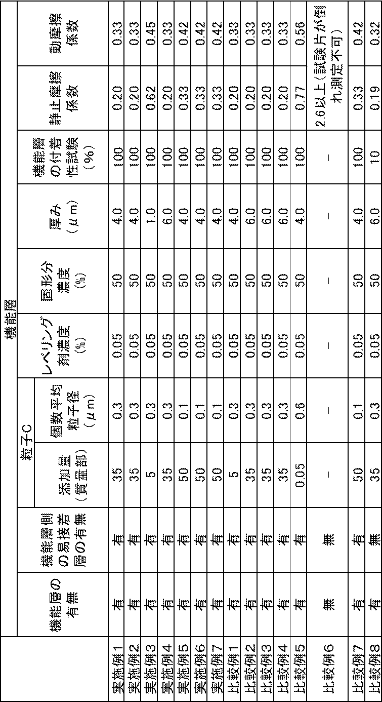
実施例1~7
真空槽に積層フィルムを投入し、1.5×10⁻⁴Paまで真空引きをした。次に、酸素導入後にアルゴンを導入し、全圧を0.6Paにした。酸素とアルゴンの流量比を表4に示す。
真空槽に積層フィルムを投入し、1.5×10⁻⁴Paまで真空引きをした。次に、酸素導入後にアルゴンを導入し、全圧を0.6Paにした。酸素とアルゴンの流量比を表4に示す。
図5に示すように、センターロール2上の積層フィルム(被処理フィルム)1の硬化型樹脂層に対して、チムニー3内のターゲット4からスパッタリングで透明導電膜を形成した。ターゲット4にはインジウム-スズ複合酸化物の焼結ターゲット(酸化スズ濃度を表4に示す。残部は酸化インジウムである)を用い、3W/cm2でDCマグネトロンスパッタリング法により透明導電膜を成膜した。膜厚は、積層フィルム(被処理フィルム)1がターゲット4上を通過するときの速度を変えることで制御した。
またスパッタリング時の成膜雰囲気のアルゴンに対する水分圧の比を、ガス分析装置(インフィコン社製、トランスペクターXPR)を用いて測定し、表4示す。表4に示すように、ボンバード工程の有無、保護フィルムの有無、フィルムロール端面の凹凸高低差、フィルムが接触走行しているセンターロールの温度を制御する温調機の温媒の温度等を調整することで、該水分圧の比を調節した。
前記ボンバード工程では、SUS(ステンレス)をターゲットとして0.5W/cm2でRFスパッタリングをした。RFスパッタリングの導入ガス量は、真空装置に導入した実施例に記載のガス量と同じとした。
保護フィルム使用時には、厚みが65μmのポリエチレンフィルムを保護フィルムとして使用した。該保護フィルムの片面にアクリル系粘着剤を塗布し、積層フィルムの透明導電膜が成膜される面とは反対の面に保護フィルムを貼り付けた。
前記温媒の温度は、フィルムロールへの成膜開始時から成膜終了時までの温度の最高値と最低値の丁度真ん中に当たる温度を表4に記載した。
透明導電膜を積層したフィルムに表4に示す熱処理を施して透明導電性フィルムを得た。得られた透明導電性フィルムの諸特性を表5に示す。
またスパッタリング時の成膜雰囲気のアルゴンに対する水分圧の比を、ガス分析装置(インフィコン社製、トランスペクターXPR)を用いて測定し、表4示す。表4に示すように、ボンバード工程の有無、保護フィルムの有無、フィルムロール端面の凹凸高低差、フィルムが接触走行しているセンターロールの温度を制御する温調機の温媒の温度等を調整することで、該水分圧の比を調節した。
前記ボンバード工程では、SUS(ステンレス)をターゲットとして0.5W/cm2でRFスパッタリングをした。RFスパッタリングの導入ガス量は、真空装置に導入した実施例に記載のガス量と同じとした。
保護フィルム使用時には、厚みが65μmのポリエチレンフィルムを保護フィルムとして使用した。該保護フィルムの片面にアクリル系粘着剤を塗布し、積層フィルムの透明導電膜が成膜される面とは反対の面に保護フィルムを貼り付けた。
前記温媒の温度は、フィルムロールへの成膜開始時から成膜終了時までの温度の最高値と最低値の丁度真ん中に当たる温度を表4に記載した。
透明導電膜を積層したフィルムに表4に示す熱処理を施して透明導電性フィルムを得た。得られた透明導電性フィルムの諸特性を表5に示す。
比較例1~8
表1~3に示す条件で作成された積層フィルムを用い、表4に示す条件で透明導電膜を形成した以外は、実施例1~7と同様にして透明導電性フィルムを作成した。なお比較例7では、ターゲット4として、インジウム-スズ複合酸化物の焼結ターゲットに変えて、酸化スズを含まない酸化インジウムの焼結ターゲットを使用した。得られた透明導電性フィルムの諸特性を表5に示す。比較例6ではオリゴマー析出に起因するムラや白点が確認された。また比較例8で一様性の評価がNGであった原因は、機能層側の易接着層がないこと及び機能層のレベリング剤が少ないことの2点により、機能層用の塗布液が透明プラスチックフィルム基材に濡れにくくなったためと推察される。
表1~3に示す条件で作成された積層フィルムを用い、表4に示す条件で透明導電膜を形成した以外は、実施例1~7と同様にして透明導電性フィルムを作成した。なお比較例7では、ターゲット4として、インジウム-スズ複合酸化物の焼結ターゲットに変えて、酸化スズを含まない酸化インジウムの焼結ターゲットを使用した。得られた透明導電性フィルムの諸特性を表5に示す。比較例6ではオリゴマー析出に起因するムラや白点が確認された。また比較例8で一様性の評価がNGであった原因は、機能層側の易接着層がないこと及び機能層のレベリング剤が少ないことの2点により、機能層用の塗布液が透明プラスチックフィルム基材に濡れにくくなったためと推察される。
なお表4中、「*1」は試験片が倒れて測定不可であったことを意味する。
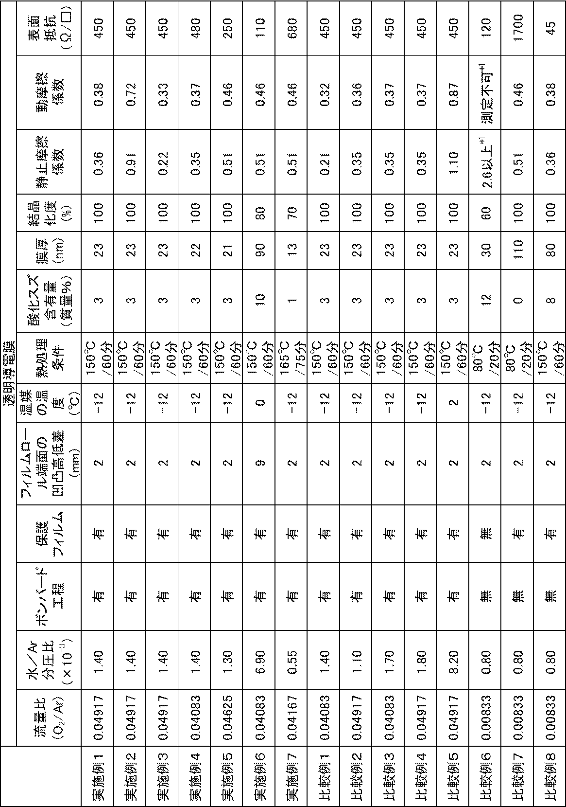

透明導電性フィルムは、液晶ディスプレイやエレクトロルミネッセンス(EL)ディスプレイ等のようなフラットパネルディスプレイや、タッチパネルの透明電極等として、電気・電子分野の用途に広く使用できる。
1 被処理フィルム
2 センターロール
3 チムニー
4 ターゲット
5 透明導電膜
6 硬化型樹脂層
7 透明プラスチックフィルム基材
8 機能層
9A 易接着層 9B 易接着層
20 透明導電性フィルム
2 センターロール
3 チムニー
4 ターゲット
5 透明導電膜
6 硬化型樹脂層
7 透明プラスチックフィルム基材
8 機能層
9A 易接着層 9B 易接着層
20 透明導電性フィルム
Claims (9)
- 透明プラスチックフィルム基材上の少なくとも一方の面にインジウム-スズ複合酸化物の透明導電膜が積層された透明導電性フィルムであって、
前記透明導電膜の平均算術平均高さ(AVSa)が2nm以上50nm以下であり、
前記透明導電膜の平均最大山高さ(AVSp)が150nm以上1000nm以下であり、
下記試験方法1から求められる前記透明導電膜側表面及び前記透明導電膜が積層された面とは反対側表面の平均突起幅が12μm以下であり、
下記試験方法2から求められる前記透明導電膜のラミネート強度が450N/15mm以上である、透明導電性フィルム。
[試験方法1]
3次元表面形状測定装置バートスキャン(測定条件:waveモード、測定波長560nm、対物レンズ50倍、視野188.709μm×141.496μm)を用いた粒子解析を以下の(i)~(v)の手順で行う。
(i)測定表面の最も低い位置から高さ0.1μmでの全突起の断面積(Tc)を求める。この測定は透明導電膜側表面及び透明導電膜が積層された面とは反対側表面の両方について行い、透明導電膜側表面と、透明導電膜が積層された面とは反対側表面における全突起の断面積の合計を全突起の断面積(Tc)とする。
(ii)全突起の断面積の平均値(全突起数をNpとしたとき、Tc/Np)を求める。
(iii)平均値(Tc/Np)の10倍以上の断面積を有する突起と、平均値(Tc/Np)の1/10倍以下の断面積を有する突起を除く。
(iv)(iii)で残った突起から断面積が大きい順に上位20%の突起と下位20%の突起をさらに除く。
(v)(iv)で残った突起について断面積の平均値(A)を計算し、その値を下記式(1)に代入して平均突起幅(B)を算出する。
式(1):平均突起幅(B)=2×(A÷π)0.5
[試験方法2]
透明導電性フィルムの透明導電膜側表面に、ウレタン系2液硬化型接着剤(溶剤としての酢酸エチルを4質量%含有)をワイヤーバー#5で塗工し、次に60℃で1分間加熱する。その後、透明導電膜の前記接着剤塗工面と、PETフィルム(厚み100μm)のPET表面を60℃でドライラミネート法(0.3MPa、幅70cm)により貼り合わせ、40℃にて4日間エージングを施すことにより、評価用のラミネート積層体を得る。得られたラミネート積層体を幅15mm、長さ150mmに切り出して試験片とし、温度23℃、相対湿度65%、剥離速度100mm/分の条件下で、T字剥離試験を行い、最大荷重を測定する。 - 前記透明導電膜の厚みが10nm以上100nm以下であり、
前記透明導電膜に含まれる酸化スズ濃度が0.5質量%以上11質量%以下であり、
前記透明導電膜の静止摩擦係数が1.00以下であり、
前記透明導電膜の動摩擦係数が0.80以下である、請求項1に記載の透明導電性フィルム。 - 前記透明導電膜の結晶化度が70%以上である請求項1又は2に記載の透明導電性フィルム。
- 前記透明プラスチックフィルム基材と前記透明導電膜の間に硬化型樹脂層を有し、
前記透明プラスチックフィルム基材の前記透明導電膜が存在する側とは反対側に機能層を有する請求項1又は2に記載の透明導電性フィルム。 - 硬化型樹脂層は、無機粒子及び有機粒子から選択される少なくとも1種以上の粒子を含む請求項4に記載の透明導電性フィルム。
- 前記機能層の静止摩擦係数が0.70以下であり、前記機能層の動摩擦係数が0.50以下である請求項4に記載の透明導電性フィルム。
- 前記機能層は、無機粒子及び有機粒子から選択される少なくとも1種以上の粒子を含む請求項4に記載の透明導電性フィルム。
- 前記透明プラスチックフィルム基材の少なくとも一方の側に易接着層を有する請求項1又は2に記載の透明導電性フィルム。
- 易接着層が、前記透明プラスチックフィルム基材と前記硬化型樹脂層との間もしくは前記透明プラスチックフィルム基材と前記機能層との間のいずれか一方、またはその両方に配置される請求項4に記載の透明導電性フィルム。
Priority Applications (1)
| Application Number | Priority Date | Filing Date | Title |
|---|---|---|---|
| CN202480011110.XA CN120584385A (zh) | 2023-06-08 | 2024-05-17 | 透明导电性膜 |
Applications Claiming Priority (2)
| Application Number | Priority Date | Filing Date | Title |
|---|---|---|---|
| JP2023-094870 | 2023-06-08 | ||
| JP2023094870A JP2024176378A (ja) | 2023-06-08 | 2023-06-08 | 透明導電性フィルム |
Publications (1)
| Publication Number | Publication Date |
|---|---|
| WO2024252899A1 true WO2024252899A1 (ja) | 2024-12-12 |
Family
ID=93795459
Family Applications (1)
| Application Number | Title | Priority Date | Filing Date |
|---|---|---|---|
| PCT/JP2024/018379 Ceased WO2024252899A1 (ja) | 2023-06-08 | 2024-05-17 | 透明導電性フィルム |
Country Status (4)
| Country | Link |
|---|---|
| JP (1) | JP2024176378A (ja) |
| CN (1) | CN120584385A (ja) |
| TW (1) | TW202506399A (ja) |
| WO (1) | WO2024252899A1 (ja) |
Cited By (1)
| Publication number | Priority date | Publication date | Assignee | Title |
|---|---|---|---|---|
| WO2026023208A1 (ja) * | 2024-07-24 | 2026-01-29 | 東洋紡株式会社 | 透明導電性フィルム |
Citations (3)
| Publication number | Priority date | Publication date | Assignee | Title |
|---|---|---|---|---|
| WO2022004228A1 (ja) * | 2020-06-30 | 2022-01-06 | 東洋紡株式会社 | 透明導電性フィルム |
| WO2022049898A1 (ja) * | 2020-09-03 | 2022-03-10 | 東洋紡株式会社 | 透明導電性フィルム |
| WO2022270356A1 (ja) * | 2021-06-22 | 2022-12-29 | 東洋紡株式会社 | 透明導電性フィルム |
-
2023
- 2023-06-08 JP JP2023094870A patent/JP2024176378A/ja not_active Withdrawn
-
2024
- 2024-05-17 WO PCT/JP2024/018379 patent/WO2024252899A1/ja not_active Ceased
- 2024-05-17 CN CN202480011110.XA patent/CN120584385A/zh active Pending
- 2024-06-06 TW TW113120993A patent/TW202506399A/zh unknown
Patent Citations (3)
| Publication number | Priority date | Publication date | Assignee | Title |
|---|---|---|---|---|
| WO2022004228A1 (ja) * | 2020-06-30 | 2022-01-06 | 東洋紡株式会社 | 透明導電性フィルム |
| WO2022049898A1 (ja) * | 2020-09-03 | 2022-03-10 | 東洋紡株式会社 | 透明導電性フィルム |
| WO2022270356A1 (ja) * | 2021-06-22 | 2022-12-29 | 東洋紡株式会社 | 透明導電性フィルム |
Cited By (1)
| Publication number | Priority date | Publication date | Assignee | Title |
|---|---|---|---|---|
| WO2026023208A1 (ja) * | 2024-07-24 | 2026-01-29 | 東洋紡株式会社 | 透明導電性フィルム |
Also Published As
| Publication number | Publication date |
|---|---|
| JP2024176378A (ja) | 2024-12-19 |
| TW202506399A (zh) | 2025-02-16 |
| CN120584385A (zh) | 2025-09-02 |
Similar Documents
| Publication | Publication Date | Title |
|---|---|---|
| JP7160100B2 (ja) | 透明導電性フィルム | |
| JP7639836B2 (ja) | 透明導電性フィルム | |
| JP7758239B2 (ja) | 透明導電性フィルム | |
| JP7677422B2 (ja) | 透明導電性フィルム | |
| JP5481992B2 (ja) | 透明導電性フィルム | |
| JP7272488B2 (ja) | 透明導電性フィルム | |
| JP2024176378A (ja) | 透明導電性フィルム | |
| JP7827129B2 (ja) | 透明導電性フィルム | |
| WO2026023208A1 (ja) | 透明導電性フィルム | |
| JP7017187B1 (ja) | 透明導電性フィルム | |
| JP5509683B2 (ja) | 透明導電性フィルム | |
| JP7582199B2 (ja) | 透明導電性フィルム | |
| WO2025263282A1 (ja) | 透明導電性フィルム | |
| JP2024180466A (ja) | 透明導電性フィルム | |
| WO2025263281A1 (ja) | 透明導電性フィルム | |
| WO2025187252A1 (ja) | 透明導電性フィルム |
Legal Events
| Date | Code | Title | Description |
|---|---|---|---|
| 121 | Ep: the epo has been informed by wipo that ep was designated in this application |
Ref document number: 24819132 Country of ref document: EP Kind code of ref document: A1 |
|
| WWE | Wipo information: entry into national phase |
Ref document number: 202480011110.X Country of ref document: CN |
|
| WWP | Wipo information: published in national office |
Ref document number: 202480011110.X Country of ref document: CN |
|
| NENP | Non-entry into the national phase |
Ref country code: DE |