WO2024252821A1 - 蓄電装置 - Google Patents
蓄電装置 Download PDFInfo
- Publication number
- WO2024252821A1 WO2024252821A1 PCT/JP2024/016333 JP2024016333W WO2024252821A1 WO 2024252821 A1 WO2024252821 A1 WO 2024252821A1 JP 2024016333 W JP2024016333 W JP 2024016333W WO 2024252821 A1 WO2024252821 A1 WO 2024252821A1
- Authority
- WO
- WIPO (PCT)
- Prior art keywords
- conductive
- foil
- current collecting
- adhesive layer
- current collector
- Prior art date
- Legal status (The legal status is an assumption and is not a legal conclusion. Google has not performed a legal analysis and makes no representation as to the accuracy of the status listed.)
- Ceased
Links
Images


Classifications
-
- H—ELECTRICITY
- H01—ELECTRIC ELEMENTS
- H01M—PROCESSES OR MEANS, e.g. BATTERIES, FOR THE DIRECT CONVERSION OF CHEMICAL ENERGY INTO ELECTRICAL ENERGY
- H01M10/00—Secondary cells; Manufacture thereof
- H01M10/04—Construction or manufacture in general
- H01M10/0413—Large-sized flat cells or batteries for motive or stationary systems with plate-like electrodes
- H01M10/0418—Large-sized flat cells or batteries for motive or stationary systems with plate-like electrodes with bipolar electrodes
-
- H—ELECTRICITY
- H01—ELECTRIC ELEMENTS
- H01G—CAPACITORS; CAPACITORS, RECTIFIERS, DETECTORS, SWITCHING DEVICES, LIGHT-SENSITIVE OR TEMPERATURE-SENSITIVE DEVICES OF THE ELECTROLYTIC TYPE
- H01G11/00—Hybrid capacitors, i.e. capacitors having different positive and negative electrodes; Electric double-layer [EDL] capacitors; Processes for the manufacture thereof or of parts thereof
- H01G11/10—Multiple hybrid or EDL capacitors, e.g. arrays or modules
- H01G11/12—Stacked hybrid or EDL capacitors
-
- H—ELECTRICITY
- H01—ELECTRIC ELEMENTS
- H01G—CAPACITORS; CAPACITORS, RECTIFIERS, DETECTORS, SWITCHING DEVICES, LIGHT-SENSITIVE OR TEMPERATURE-SENSITIVE DEVICES OF THE ELECTROLYTIC TYPE
- H01G11/00—Hybrid capacitors, i.e. capacitors having different positive and negative electrodes; Electric double-layer [EDL] capacitors; Processes for the manufacture thereof or of parts thereof
- H01G11/66—Current collectors
- H01G11/68—Current collectors characterised by their material
-
- H—ELECTRICITY
- H01—ELECTRIC ELEMENTS
- H01G—CAPACITORS; CAPACITORS, RECTIFIERS, DETECTORS, SWITCHING DEVICES, LIGHT-SENSITIVE OR TEMPERATURE-SENSITIVE DEVICES OF THE ELECTROLYTIC TYPE
- H01G11/00—Hybrid capacitors, i.e. capacitors having different positive and negative electrodes; Electric double-layer [EDL] capacitors; Processes for the manufacture thereof or of parts thereof
- H01G11/66—Current collectors
- H01G11/70—Current collectors characterised by their structure
-
- H—ELECTRICITY
- H01—ELECTRIC ELEMENTS
- H01M—PROCESSES OR MEANS, e.g. BATTERIES, FOR THE DIRECT CONVERSION OF CHEMICAL ENERGY INTO ELECTRICAL ENERGY
- H01M4/00—Electrodes
- H01M4/02—Electrodes composed of, or comprising, active material
- H01M4/64—Carriers or collectors
- H01M4/66—Selection of materials
- H01M4/665—Composites
- H01M4/667—Composites in the form of layers, e.g. coatings
-
- H—ELECTRICITY
- H01—ELECTRIC ELEMENTS
- H01M—PROCESSES OR MEANS, e.g. BATTERIES, FOR THE DIRECT CONVERSION OF CHEMICAL ENERGY INTO ELECTRICAL ENERGY
- H01M4/00—Electrodes
- H01M4/02—Electrodes composed of, or comprising, active material
- H01M4/64—Carriers or collectors
- H01M4/66—Selection of materials
- H01M4/668—Composites of electroconductive material and synthetic resins
-
- H—ELECTRICITY
- H01—ELECTRIC ELEMENTS
- H01M—PROCESSES OR MEANS, e.g. BATTERIES, FOR THE DIRECT CONVERSION OF CHEMICAL ENERGY INTO ELECTRICAL ENERGY
- H01M4/00—Electrodes
- H01M4/02—Electrodes composed of, or comprising, active material
- H01M2004/026—Electrodes composed of, or comprising, active material characterised by the polarity
- H01M2004/029—Bipolar electrodes
-
- H—ELECTRICITY
- H01—ELECTRIC ELEMENTS
- H01M—PROCESSES OR MEANS, e.g. BATTERIES, FOR THE DIRECT CONVERSION OF CHEMICAL ENERGY INTO ELECTRICAL ENERGY
- H01M2220/00—Batteries for particular applications
- H01M2220/20—Batteries in motive systems, e.g. vehicle, ship, plane
-
- Y—GENERAL TAGGING OF NEW TECHNOLOGICAL DEVELOPMENTS; GENERAL TAGGING OF CROSS-SECTIONAL TECHNOLOGIES SPANNING OVER SEVERAL SECTIONS OF THE IPC; TECHNICAL SUBJECTS COVERED BY FORMER USPC CROSS-REFERENCE ART COLLECTIONS [XRACs] AND DIGESTS
- Y02—TECHNOLOGIES OR APPLICATIONS FOR MITIGATION OR ADAPTATION AGAINST CLIMATE CHANGE
- Y02E—REDUCTION OF GREENHOUSE GAS [GHG] EMISSIONS, RELATED TO ENERGY GENERATION, TRANSMISSION OR DISTRIBUTION
- Y02E60/00—Enabling technologies; Technologies with a potential or indirect contribution to GHG emissions mitigation
- Y02E60/10—Energy storage using batteries
-
- Y—GENERAL TAGGING OF NEW TECHNOLOGICAL DEVELOPMENTS; GENERAL TAGGING OF CROSS-SECTIONAL TECHNOLOGIES SPANNING OVER SEVERAL SECTIONS OF THE IPC; TECHNICAL SUBJECTS COVERED BY FORMER USPC CROSS-REFERENCE ART COLLECTIONS [XRACs] AND DIGESTS
- Y02—TECHNOLOGIES OR APPLICATIONS FOR MITIGATION OR ADAPTATION AGAINST CLIMATE CHANGE
- Y02P—CLIMATE CHANGE MITIGATION TECHNOLOGIES IN THE PRODUCTION OR PROCESSING OF GOODS
- Y02P70/00—Climate change mitigation technologies in the production process for final industrial or consumer products
- Y02P70/50—Manufacturing or production processes characterised by the final manufactured product
Definitions
- This disclosure relates to an electricity storage device.
- An example of a conventional power storage device is the bipolar battery described in Patent Document 1.
- This conventional bipolar battery has multiple bipolar electrodes, each of which has a positive electrode active material layer formed on one side of a current collector and a negative electrode active material layer formed on the other side.
- the bipolar battery is constructed by stacking these bipolar electrodes with a gel electrolyte layer sandwiched between them.
- a structure in which metal foils of different materials are laminated together via a conductive adhesive may be used.
- the conductive adhesive may be, for example, a thermosetting resin that is the main component of the adhesive, in which a particulate conductive assistant (conductive particles) such as a conductive filler is dispersed.
- a particulate conductive assistant conductive particles
- Carbon black is a widely known example of a conductive assistant.
- a conductive adhesive using carbon black as a conductive assistant is used to bond laminated foils, in order to sufficiently reduce the resistance value of the laminated foils, it is necessary to include a large amount of carbon black in the conductive adhesive. In this case, a problem occurs in that the adhesive strength of the laminated foils decreases.
- the present disclosure aims to provide an energy storage device equipped with a bipolar electrode having a laminated foil that exhibits good bonding strength and good electrical conductivity.
- the energy storage device is an energy storage device including a plurality of bipolar electrodes overlapping each other in the stacking direction, each of the plurality of bipolar electrodes including a first current collecting foil and a second current collecting foil overlapping each other in the stacking direction, a conductive adhesive layer located between the first current collecting foil and the second current collecting foil and bonded to the first current collecting foil and the second current collecting foil, a first active material layer located on the surface of the first current collecting foil, and a second active material layer located on the surface of the second current collecting foil, the conductive adhesive layer includes an adhesive and a conductive assistant dispersed in the adhesive, the conductive assistant is a spherical particle having a spherical core and a conductive film covering the core, the conductive assistant is added at a rate of 0.1% by volume or more and 1.0% by volume or less, and a first value obtained by adding twice the standard deviation of the particle size of the conductive assistant to the average particle size of the conductive assistant is equal to or more
- each of the bipolar electrodes has a laminated foil in which a first current collecting foil and a second current collecting foil are bonded to each other via a conductive adhesive layer.
- the conductive assistant dispersed in the adhesive in the conductive adhesive layer is a spherical particle having a spherical core and a conductive film covering the core, the conductive assistant is added at a rate of 0.1% by volume to 1.0% by volume, and a first value obtained by adding twice the standard deviation of the particle size of the conductive assistant to the average particle size of the conductive assistant is equal to or greater than the thickness of the conductive adhesive layer.
- the above-mentioned power storage device can be provided with a bipolar electrode that exhibits good bonding strength and conductivity.
- the average particle size of the conductive additive may be larger than the thickness of the conductive adhesive layer. In this case, better electrical conduction between the first current collecting foil and the second current collecting foil is achieved via the conductive additive.
- the first current collecting foil and the second current collecting foil each have a rectangular shape, the length of one side of the first current collecting foil and the length of one side of the second current collecting foil each are 500 mm or more, and the CV value of the particle size of the conductive assistant in the conductive adhesive layer may be 10% or less.
- the conductive assistant having a particle size significantly larger than the thickness of the conductive adhesive layer is unlikely to be present in the conductive adhesive layer.
- the resistance of the bipolar electrode is unlikely to increase due to deformation of the first current collecting foil and/or the second current collecting foil due to the air.
- each of the first current collecting foil and the second current collecting foil can be well bonded to the conductive adhesive layer.
- the first current collecting foil and the second current collecting foil each have a rectangular shape, and the length of one side of the first current collecting foil and the length of one side of the second current collecting foil are each 500 mm or more, and the second value obtained by adding the average particle size of the conductive assistant to three times the standard deviation may be equal to or less than twice the thickness of the conductive adhesive layer.
- a conductive assistant having a particle size significantly larger than the thickness of the conductive adhesive layer is unlikely to be present in the conductive adhesive layer.
- the bipolar electrode is enlarged, air is unlikely to be trapped between the first current collecting foil and the second current collecting foil due to the conductive assistant.
- each of the first current collecting foil and the second current collecting foil can be well bonded to the conductive adhesive layer.
- the thickness of the first current collecting foil is at least twice the thickness of the second current collecting foil, the thickness of the second current collecting foil is less than 10 ⁇ m, the thickness of the conductive adhesive layer is less than the thickness of the second current collecting foil, and the CV value of the particle size of the conductive additive in the conductive adhesive layer may be 10% or less.
- conductive additives having particle sizes significantly larger than the thickness of the conductive adhesive layer are unlikely to be present in the conductive adhesive layer. This makes it difficult for air to be trapped between the first current collecting foil and the second current collecting foil due to the conductive additive. This makes it difficult for the resistance of the bipolar electrode to increase due to deformation of the current collecting foil (especially the second current collecting foil) due to the air.
- the conductive adhesive layer may further contain an epoxy-based hardener as a hardener, in addition to the olefin-based adhesive as an adhesive.
- the adhesive can exhibit high electrolyte resistance, and therefore good bonding strength can be exhibited over a long period of time.
- an epoxy-based hardener as a hardener when an olefin-based adhesive is used as an adhesive, gas generation during the hardening reaction between the adhesive and hardener that occurs during the production of the current collector can be effectively reduced.
- an electricity storage device that has a laminated foil in which multiple metal foils are bonded together via a conductive adhesive, and that is equipped with a bipolar electrode current collector that exhibits good bonding strength and good electrical conductivity.
- FIG. 1 is a schematic cross-sectional view showing an electricity storage device according to one embodiment.
- FIG. 2 is an enlarged view of a main portion of FIG.
- FIG. 3A is an enlarged cross-sectional view of a main portion of a current collector
- FIG. 3B is an enlarged cross-sectional view of a conductive assistant.
- FIG. 4 is a schematic diagram showing a coating device used in the production of a current collector.
- FIG. 5(a) is a diagram showing the particle size distribution of the first conductive assistant dispersed in the conductive adhesive layer
- FIG. 5(b) is a diagram showing the relationship between the thickness of the conductive adhesive layer and the resistance value of the sample.
- FIG. 8 shows the particle size distribution of the second conductive assistant contained in the 11th sample and the 12th sample.
- FIG. 1 is a schematic cross-sectional view showing an energy storage device according to one embodiment.
- FIG. 2 is an enlarged view of a main portion of FIG. 1.
- the energy storage device 1 shown in FIG. 1 is a device (vehicle energy storage battery) used in batteries of various vehicles such as forklifts, hybrid cars, and electric cars.
- the energy storage device 1 is a secondary battery such as a nickel-metal hydride secondary battery or a lithium-ion secondary battery.
- the energy storage device 1 may be an electric double layer capacitor or an all-solid-state battery. The following describes an example in which the energy storage device 1 is a lithium-ion secondary battery.
- the energy storage device 1 comprises an electrode stack 2, which is a stack of multiple bipolar electrodes 14, and a sealing body 3 that seals the side surfaces 2a of the electrode stack 2 that extend in the stacking direction D of the bipolar electrodes 14. For this reason, the energy storage device 1 is also called a vehicle bipolar battery.
- the electrode stack 2 comprises multiple cells 4. Each cell 4 has a positive electrode 11, a negative electrode 12, and a separator 13.
- the positive electrode 11 and the negative electrode 12 are, for example, rectangular when viewed from the stacking direction D.
- the positive electrode 11 and the negative electrode 12 are arranged facing each other with the separator 13 in between.
- the facing direction of the positive electrode 11 and the negative electrode 12 coincides with the stacking direction D of the bipolar electrode 14.
- the positive electrode 11 is composed of a current collector 21 and a positive electrode active material layer 23 provided on a first surface 21a of the current collector 21.
- the negative electrode 12 is composed of a current collector 21 and a negative electrode active material layer 24 provided on a second surface 21b of the current collector 21.
- FIG. 3 is an enlarged cross-sectional view of a main part of the current collector.
- the current collector 21 is a chemically inactive electrical conductor for continuing to pass current to the positive electrode active material layer 23 and the negative electrode active material layer 24 during discharging or charging of the lithium ion secondary battery, and is a member (bipolar electrode current collector) used in the bipolar electrode 14.
- the current collector 21 has a three-layer structure having a first current collector foil 21A, a second current collector foil 21B, and a conductive adhesive layer 22 located between the first current collector foil 21A and the second current collector foil 21B and bonding the first current collector foil 21A and the second current collector foil 21B.
- Each of the first current collecting foil 21A and the second current collecting foil 21B is a conductive member having, for example, a rectangular shape when viewed from the stacking direction D.
- the first current collecting foil 21A and the second current collecting foil 21B are integrated with each other via the conductive adhesive layer 22.
- the first current collecting foil 21A and the second current collecting foil 21B overlapping each other along the stacking direction D are electrically connected to each other via the conductive adhesive layer 22.
- the first surface 21Aa of the first current collecting foil 21A is an exposed surface (surface) located on the opposite side to the surface in contact with the conductive adhesive layer 22, and corresponds to the first surface 21a of the current collector 21.
- the second surface 21Ab of the first current collecting foil 21A is a surface bonded to the conductive adhesive layer 22.
- the first surface 21Ba of the second current collecting foil 21B is an exposed surface (surface) located on the opposite side to the surface in contact with the conductive adhesive layer 22, and corresponds to the second surface 21b of the current collector 21.
- the second surface 21Bb of the second current collecting foil 21B is the surface that is bonded to the conductive adhesive layer 22.
- the length of one side of the first current collecting foil 21A and the length of one side of the second current collecting foil 21B are each 500 mm or more. The length may be 750 mm or more, 1000 mm or more, or 1200 mm or more.
- each cell 4 included in the electrode stack 2 the positive electrode 11 is composed of a portion of a specific bipolar electrode 14, and the negative electrode 12 is composed of a portion of another bipolar electrode 14.
- a plurality of cells 4 are formed by alternately stacking bipolar electrodes 14 and separators 13. Thus, a plurality of cells 4 are electrically connected in series.
- the same bipolar electrode 14 may be shared between adjacent cells 4, 4 in the stacking direction D.
- a terminal electrode (positive terminal electrode) including a first current collecting foil 21A is disposed.
- a terminal electrode (negative terminal electrode) including a second current collecting foil 21B is disposed.
- the first current collecting foil 21A and the second current collecting foil 21B may be formed, for example, in a plate-like, foil-like, sheet-like, film-like, or other form.
- first current collecting foil 21A and the second current collecting foil 21B are metal foils, for example, aluminum foil, copper foil, nickel foil, titanium foil, or stainless steel foil is used.
- the first current collecting foil 21A is, for example, an aluminum foil.
- the second current collecting foil 21B is, for example, a copper foil.
- the first current collecting foil 21A and the second current collecting foil 21B may be an alloy foil or clad foil of the above metals.
- the thickness of the first current collecting foil 21A and the second current collecting foil 21B along the stacking direction D may each be in the range of 1 ⁇ m to 150 ⁇ m. From the viewpoint of durability of the current collector 21, at least one of the thicknesses of the first current collector foil 21A and the second current collector foil 21B may be 50 ⁇ m or more, 40 ⁇ m or more, or 30 ⁇ m or more.
- the thickness of one of the first current collector foil 21A and the second current collector foil 21B is, for example, 1 ⁇ m or more and less than 10 ⁇ m, and the thickness of the other is, for example, 20 ⁇ m or more and 150 ⁇ m or less.
- one of the first current collector foil 21A and the second current collector foil 21B is a thin current collector foil with a thickness of less than 10 ⁇ m
- the other of the first current collector foil 21A and the second current collector foil 21B is a current collector foil having a thickness at least twice that of the thin current collector foil.
- the first current collecting foil 21A is an aluminum foil
- the second current collecting foil 21B is a copper foil.
- the aluminum foil of the first current collecting foil 21A and the copper foil of the second current collecting foil 21B are integrated by bonding via the conductive adhesive layer 22. Therefore, the current collector 21 can be said to be a foil (laminate foil) in which the first current collecting foil 21A and the second current collecting foil 21B are bonded to each other via the conductive adhesive layer 22. From the viewpoints of cost, weight, etc., the thickness of the first current collecting foil 21A in the current collector 21 is greater than the thickness of the second current collecting foil 21B.
- the thickness of the first current collecting foil 21A included in the bipolar electrode 14 is, for example, 40 ⁇ m or more and 100 ⁇ m or less. From the viewpoint of the strength of the current collector 21, the thickness of the first current collecting foil 21A may be five times or more the thickness of the second current collecting foil 21B. In this case, for example, even if the thickness of the second current collector foil 21B is 9 ⁇ m or less, the thickness of the first current collector foil 21A can be 45 ⁇ m or more, so that the strength of the current collector 21 can be sufficient as a laminated foil.
- the thickness of the second current collector foil 21B included in the bipolar electrode 14 is, for example, 5 ⁇ m or more and less than 10 ⁇ m.
- the thickness of the first current collector foil 21A included in the positive terminal electrode constituting the outermost electrode of the electrode laminate 2 may be 100 ⁇ m or more and 150 ⁇ m or less.
- the same laminated foil as the current collector 21 is used as the negative terminal electrode constituting the outermost electrode of the electrode laminate 2.
- the thickness of the first current collector foil included in the negative terminal electrode may be 100 ⁇ m or more and 150 ⁇ m or less. In other words, by making the first current collector foil thick, the thin second current collector foil can be reinforced.
- the conductive adhesive layer 22 is an anisotropic conductive member that bonds the first current collector foil 21A and the second current collector foil 21B to integrate them with each other, and is located between the first current collector foil 21A and the second current collector foil 21B in the stacking direction D.
- the conductive adhesive layer 22 is a member that electrically connects the first current collector foil 21A and the second current collector foil 21B to each other. From the viewpoints of ensuring the bonding strength between the first current collector foil 21A and the second current collector foil 21B, reducing the internal resistance of the current collector 21, and reducing the thickness of the current collector 21, the thickness TH of the conductive adhesive layer 22 is, for example, 2 ⁇ m or more and 5 ⁇ m or less.
- the conductive adhesive layer 22 has an adhesive 40 and a plurality of conductive assistants 50 dispersed in the adhesive 40.
- the adhesive 40 includes a resin that exhibits adhesiveness to both the first current collecting foil 21A and the second current collecting foil 21B.
- the resin include olefin-based resins such as polyethylene, polypropylene, and polybutylene, ethylene-vinyl acetate copolymer (EVA), polyethylene terephthalate (PET), polyethylene naphthalate (PEN), polyethernitrile (PEN), polyimide (PI), polyamide (PA), polytetrafluoroethylene (PTFE), styrene-butadiene rubber (SBR), polyacrylonitrile (PAN), polymethyl acrylate (PMA), polymethyl methacrylate (PMMA), polyvinyl chloride (PVC), polyvinylidene fluoride (PVDF), silicone, epoxy resin, or a mixture thereof.
- olefin-based resins such as polyethylene, polypropylene, and polybutylene, ethylene-vinyl acetate copolymer (EVA), polyethylene
- the above-mentioned resin may be an olefin-based resin adhesive (olefin-based adhesive such as polyethylene or polypropylene).
- olefin-based adhesive such as polyethylene or polypropylene
- the molecular weight of the olefin-based adhesive is, for example, tens of thousands or less.
- the resin in the adhesive 40 has good dispersibility in the solvent.
- the olefin-based adhesive is low-molecular-weight polypropylene (polypropylene with a molecular weight of tens of thousands or less).
- the thickness of the adhesive 40 corresponds to the thickness TH of the conductive adhesive layer 22.
- the adhesive 40 may contain various additives such as a hardener, an antiblocking agent, an antioxidant, and a light stabilizer.
- a hardener When the resin is an olefin-based resin adhesive, the hardener may be, for example, an isocyanate-based hardener or an epoxy-based hardener.
- an epoxy-based hardener When two metal foils are joined with an adhesive containing an olefin-based resin as an adhesive component, an epoxy-based hardener may be used as the hardener to prevent gas generation associated with the hardening reaction.
- the conductive assistant 50 is a member that serves as a conductive path between the first collector foil 21A and the second collector foil 21B in the conductive adhesive layer 22, and is dispersed in the adhesive 40.
- Spherical particles are used as the conductive assistant 50.
- the spherical particles may include not only perfectly spherical particles but also elliptical spherical particles.
- the conductive assistant 50 has a spherical core 51 and a conductive film 52 that covers the core 51.
- the core 51 is the main body of the conductive assistant 50 and is a member that exhibits a spherical shape.
- the member that forms the core 51 may be, for example, a ceramic material such as silica, or a resin material such as epoxy resin, acrylic resin, urethane resin, nylon resin, or silicone resin.
- the conductive film 52 is a part that exhibits electrical conductivity in the conductive assistant 50, and covers the entire core 51.
- the conductive film 52 is, for example, a metal thin film, an alloy thin film, or the like that coats the core 51.
- the metal thin films and alloy thin films contain metals such as gold, silver, copper, platinum, nickel, palladium, and aluminum.
- the particle diameter DA is larger than the thickness TH of the conductive adhesive layer 22. Therefore, some of the conductive assistants 50 are exposed from the adhesive 40 and can contact both the first current collector foil 21A and the second current collector foil 21B.
- the first current collector foil 21A and the second current collector foil 21B are conductive to each other through the conductive assistants 50.
- the average particle diameter of the conductive assistant 50 is D50 and the standard deviation of the particle diameter DA of the conductive assistant 50 is ⁇
- the value obtained by adding the average particle diameter of the conductive assistant 50 to the value obtained by multiplying the standard deviation of the particle diameter DA of the conductive assistant 50 by two (D50+2 ⁇ , first value) is larger than the thickness TH of the conductive adhesive layer 22.
- the average particle size of the conductive assistant 50 is larger than the thickness of the adhesive 40.
- the value (D50+ ⁇ ) obtained by adding the standard deviation of the particle size DA of the conductive assistant 50 to the average particle size of the conductive assistant 50 is also larger than the thickness TH of the conductive adhesive layer 22.
- the particle size distribution of the conductive assistant 50 is measured by a known method such as the Coulter method, image analysis, or laser diffraction/scattering method.
- the particle size DA of the conductive assistant 50 corresponds to the maximum distance between any two points on the contour of the conductive assistant 50 obtained using an observation means such as a scanning electron microscope (SEM) or a transmission electron microscope (TEM).
- the average particle size (D50) of the conductive assistant 50 refers to the particle size when the number (or mass) of particles larger than a certain particle size accounts for 50% of the number (or mass) of all measured particles in the particle size distribution of the measured particles.
- D10 refers to the particle size when the number (or mass) of particles larger than a certain particle size accounts for 10% of the number (or mass) of all measured particles in the particle size distribution of the measured particles.
- D90 refers to the particle size when the number (or mass) of particles larger than a certain particle size accounts for 90% of the number (or mass) of all measured particles in the particle size distribution of the measured particles.
- the average particle size of the conductive assistant 50 corresponds to the particle size when the cumulative value in the volume-based cumulative particle size distribution obtained by the laser diffraction/scattering method for the powder is 50%.
- the particle size when the cumulative value is 10% corresponds to D10
- the particle size when the cumulative value is 90% corresponds to D90.
- the values representing the variation in particle size distribution of the conductive assistant 50 calculated by the formulas "(D50-D10)/D50” and “(D90-D50)/D50” may be 0.5 or less, 0.3 or less, or 0.1 or less.
- the standard deviation of the particle size DA of the conductive assistant 50 corresponds to the standard deviation calculated from the particle sizes of 10,000 to 30,000 particles, for example.
- the value (D50+3 ⁇ , second value) obtained by adding three times the standard deviation of the particle diameter DA of the conductive additive 50 to the average particle diameter of the conductive additive 50 is equal to or less than two times the thickness TH of the conductive adhesive layer 22.
- conductive additive 50 having an extremely large particle diameter is not contained in the conductive adhesive layer 22, or is almost not contained therein. This makes it difficult for air to be trapped during the manufacture of the current collector 21 (i.e., it is difficult for an area where air remains between the first current collector foil 21A and the second current collector foil 21B during the manufacture of the current collector 21). This makes it possible to suppress an increase in the internal resistance of the current collector 21 caused by the air (details will be described later).
- the CV value (coefficient of variation) of the particle diameter DA of the conductive assistant 50 in the conductive adhesive layer 22 may be 10% or less.
- the CV value of the particle diameter DA of the conductive assistant 50 may be 7% or less, 5% or less, or 3% or less.
- a low CV value of the particle diameter means that the particles are monodispersed well.
- the lower the CV value of the particle diameter DA of the conductive assistant 50 the narrower the particle diameter distribution of the conductive assistant 50.
- the CV value of the particle diameter DA of the conductive assistant 50 is 10% or less, it can be said that the conductive assistant 50 having an extremely large particle diameter is not contained in the conductive adhesive layer 22, or is almost not contained therein. For this reason, air entrapment is less likely to occur during the manufacture of the current collector 21 (i.e., a region in which air remains between the first current collector foil 21A and the second current collector foil 21B is less likely to be formed during the manufacture of the current collector 21). This prevents the internal resistance of the current collector 21 from increasing due to the air (details will be described later).
- the proportion of conductive additive 50 added to conductive adhesive layer 22 is 0.1 volume % or more and 1.0 volume % or less. In this case, the internal resistance of current collector 21 can be reduced while ensuring the bonding strength between first current collector foil 21A and second current collector foil 21B via conductive adhesive layer 22.
- the proportion may be 0.1 volume % or more and 0.8 volume % or less, 0.2 volume % or more and 0.8 volume % or less, 0.4 volume % or more and 0.6 volume % or less, or 0.1 volume % or more and 0.5 volume % or less.
- the positive electrode active material layer 23 is a member (first active material layer) provided in a rectangular shape in the center of the first surface 21Aa of the rectangular first current collector foil 21A in a plan view.
- the negative electrode active material layer 24 is a member (second active material layer) provided in a rectangular shape in the center of the first surface 21Ba of the rectangular second current collector foil 21B in a plan view.
- an area where the positive electrode active material layer 23 is not provided is formed on the first surface 21Aa side, and an area where the negative electrode active material layer 24 is not provided is formed on the first surface 21Ba side.
- the negative electrode active material layer 24 is formed to be slightly larger than the positive electrode active material layer 23. When viewed from the stacking direction D, the entire formation area of the positive electrode active material layer 23 is located within the formation area of the negative electrode active material layer 24.
- the positive electrode active material layer 23 includes a positive electrode active material capable of absorbing and releasing charge carriers such as lithium ions.
- the positive electrode active material include composite oxides, metallic lithium, and sulfur.
- the composition of the composite oxide includes at least one of iron, manganese, titanium, nickel, cobalt, and aluminum, and lithium.
- the composite oxide include olivine-type lithium iron phosphate (LiFePO 4 ), lithium cobalt oxide (LiCoO 2 ), and lithium nickel cobalt manganese oxide (LiNiMnCoO 2 ).
- the negative electrode active material layer 24 includes a negative electrode active material capable of absorbing and releasing charge carriers such as lithium ions.
- the negative electrode active material include graphite, artificial graphite, highly oriented graphite, mesocarbon microbeads, hard carbon, soft carbon, and other carbon, metal compounds, elements or compounds thereof that can be alloyed with lithium, boron-doped carbon, and the like.
- elements that can be alloyed with lithium include silicon (Si) and tin.
- the positive electrode active material layer 23 and the negative electrode active material layer 24 may contain a binder and a conductive assistant in addition to the active material.
- the binder serves to connect the active material or the conductive assistant to each other and maintain the conductive network in the electrode.
- the binder include fluorine-containing resins such as polyvinylidene fluoride, polytetrafluoroethylene, and fluorine rubber, thermoplastic resins such as polypropylene and polyethylene, imide resins such as polyimide and polyamideimide, alkoxysilyl group-containing resins, acrylic resins such as polyacrylic acid and polymethacrylic acid, styrene-butadiene rubber, carboxymethyl cellulose, alginates such as sodium alginate and ammonium alginate, water-soluble cellulose ester crosslinked bodies, and starch-acrylic acid graft polymers.
- fluorine-containing resins such as polyvinylidene fluoride, polytetrafluoroethylene, and fluor
- the conductive assistant is, for example, a conductive material such as acetylene black, carbon black, and graphite, and can increase electrical conductivity.
- a conductive material such as acetylene black, carbon black, and graphite
- N-methyl-2-pyrrolidone is used as the viscosity adjusting solvent.
- the positive electrode active material layer 23 and the negative electrode active material layer 24 can be formed on the current collector 21 by known methods such as roll coating, die coating, dip coating, doctor blade, spray coating, and curtain coating. Specifically, an active material, a solvent, and, if necessary, a binder and a conductive assistant are mixed to produce a slurry-like active material layer forming composition, which is then applied to the current collector 21 and dried.
- the solvent that can be used include N-methyl-2-pyrrolidone, methanol, methyl isobutyl ketone, and water.
- the dried active material layer forming composition may be compressed to increase the electrode density.
- the separator 13 is disposed between the positive electrode 11 and the negative electrode 12 in the stacking direction D.
- the separator 13 is a member that isolates the adjacent positive electrode 11 and negative electrode 12 in the electrode stack 2, thereby preventing an electrical short circuit caused by contact between the two electrodes while allowing charge carriers such as lithium ions to pass through.
- the separator 13 is disposed between the positive electrode active material layer 23 and the negative electrode active material layer 24 that face each other in the stacking direction D.
- the separator 13 When viewed from the stacking direction D, the separator 13 has a rectangular shape that is slightly larger than the positive electrode active material layer 23 and the negative electrode active material layer 24 and slightly smaller than the current collector 21. When viewed from the stacking direction D, the end 13a of the separator 13 is located outside the positive electrode active material layer 23 and the negative electrode active material layer 24. The end 13a of the separator 13 is welded to a sealing member 32, which will be described later.
- the separator 13 is formed, for example, in a sheet shape.
- the separator 13 is composed of, for example, a porous sheet or nonwoven fabric containing a polymer that absorbs and retains an electrolyte. Examples of materials that constitute the separator 13 include polypropylene, polyethylene, polyolefin, and polyester.
- the separator 13 may have a single-layer structure or a multi-layer structure. In the case of a multi-layer structure, the separator 13 may include, for example, a base material layer and a pair of adhesive layers, and may be bonded and fixed to the positive electrode active material layer 23 and the negative electrode active material layer 24 by the pair of adhesive layers.
- the separator 13 may include a ceramic layer that serves as a heat-resistant layer.
- the separator 13 may be reinforced with a vinylidene fluoride resin compound such as polyvinylidene fluoride.
- Examples of the electrolyte impregnated in the separator 13 include a liquid electrolyte (electrolytic solution) containing a non-aqueous solvent and an electrolyte salt dissolved in the non-aqueous solvent, and a polymer gel electrolyte containing an electrolyte held in a polymer matrix.
- the electrolyte salt may be a known lithium salt such as LiFSI, LiClO 4 , LiAsF 6 , LiPF 6 , LiBF 4 , LiCF 3 SO 3 , LiN(FSO 2 ) 2 , or LiN(CF 3 SO 2 ) 2.
- the non-aqueous solvent may be a known solvent such as cyclic carbonates, cyclic esters, chain carbonates, chain esters, or ethers. Two or more of these known solvent materials may be used in combination.
- the sealing body 3 is a member that seals the side surface 2a extending in the stacking direction D of the electrode stack 2.
- the sealing body 3 maintains the distance between a pair of adjacent current collectors 21, 21 in the stacking direction D so that they do not come into contact with each other, and seals the space S between the pair of current collectors 21, 21.
- the space S is defined by the sealing body 3 and the adjacent current collectors 21, 21 in the stacking direction D.
- the space S contains the positive electrode active material layer 23, the negative electrode active material layer 24, the separator 13, and the electrolyte.
- the sealing body 3 is composed of a plurality of frame-shaped spacers 31 and a plurality of frame-shaped sealing members 32.
- the spacers 31 and the sealing members 32 are each composed of a resin material.
- the sealing members 32 are welded to the edge portions 21c on both sides of the current collector 21 included in the bipolar electrode 14, on both sides of the first current collector foil 21A included in the positive terminal electrode, and on both sides of the second current collector foil 21B included in the negative terminal electrode.
- the sealing members 32 are provided so as to cover the edge portions 21c of the current collector 21.
- the sealing members 32 contact both the first surface 21a and the second surface 21b at the edge portions 21c of the current collector 21, and are also located on the side end surfaces 21d of the current collector 21 so as to connect them.
- the spacers 31 are disposed between the current collectors 21, 21 adjacent to each other in the stacking direction D, and between the seal members 32, 32 adjacent to each other in the stacking direction D.
- the sealing member 32 has an overlapping portion that overlaps with the current collector 21 in the stacking direction D, and a protruding portion that protrudes outward beyond the edge portion 21c of the current collector 21 and does not overlap with the current collector 21 in the stacking direction D.
- the sealing member 32 is welded to the first surface 21a over the entire overlapping portion with the first surface 21a, and is welded to the second surface 21b over the entire overlapping portion with the second surface 21b.
- the sealing member 32 covers the side end surface 21d of the current collector 21 at the protruding portion.
- the sealing member 32 covers the side end surface 21d of the current collector 21 by welding a first seal arranged on one side of the current collector 21 and a second seal arranged on the other side of the current collector 21 to each other at the protruding portion.
- the spacer 31 is a member that maintains a predetermined distance between adjacent current collectors 21, 21 in the stacking direction D.
- the spacer 31 is disposed between the sealing members 32, 32 that cover the edge portions 21c of the current collectors 21, 21 that are adjacent in the stacking direction D.
- the thickness T2 of the spacer 31 is greater than the thickness T1 of the portion of the sealing member 32 that is welded to one side of the current collector 21.
- the sealing member 32 is provided to cover the edge portion 21c of the current collector 21, and the thickness of the portion of the sealing member 32 located on the first surface 21a of the current collector 21 is equal to the thickness of the portion of the sealing member 32 located on the second surface 21b of the current collector 21.
- the thickness T1 of the sealing member 32 is defined by the thickness of the portion of the sealing member 32 located on the second surface 21b of the current collector 21.
- the thickness T2 of the spacer 31 is defined by the thickness of the portion located between the sealing members 32, 32 adjacent to each other in the stacking direction D.
- the ratio of the thickness T2 of the spacer 31 to the thickness T1 of the sealing member 32 is, for example, 1:2 to 1:4.
- the outer edge 32a of the sealing member 32 and the outer edge 31a of the spacer 31 both protrude outward from the edge 21c of the current collector 21 when viewed from the stacking direction D.
- the outer edge 31a of each spacer 31 protruding outward from the edge 21c of the current collector 21 and the outer edge 32a of the sealing member 32 adjacent to the spacer 31 in the stacking direction D are welded to each other at their end faces to form a welded portion W.
- the outer surface 3a of the sealing body 3 is formed by this welded portion W.
- the outer edge 31a of the spacer 31 and the outer edge 32a of the sealing member 32 can be welded to each other by a method such as infrared welding or hot plate welding. In the welded portion W, the compatibility of the resin material constituting the sealing member 32 and the resin material constituting the spacer 31 ensures the sealing of the space S between the adjacent current collectors 21, 21 in the stacking direction D.
- the spacer 31 is not welded to either the seal member 32 in contact with one of the current collectors 21 adjacent to each other in the stacking direction D or the seal member 32 in contact with the other current collector 21.
- the spacer 31 and the seal member 32 in contact with one of the current collectors 21 may be in contact with each other or may be slightly spaced apart.
- the spacer 31 and the seal member 32 in contact with the other current collector 21 may be in contact with each other or may be slightly spaced apart.
- the spacer 31 is not welded to either of the current collectors 21, 21 adjacent to each other in the stacking direction D.
- the end 13a of the separator 13 described above is welded to the inner edge 32b of the seal member 32.
- the inner edge 32b of the seal member 32 is aligned with the inner edge 31b of the spacer 31, but this is not limited to the above.
- the inner edge of the seal member 32 may be misaligned with the inner edge of the spacer 31.
- the inner edge 32b of the seal member 32 may protrude further inwardly than the inner edge 31b of the spacer 31, or the inner edge 31b may protrude further inwardly than the inner edge 32b of the seal member 32.
- the resin material constituting the sealing member 32 and the spacer 31 may be, for example, a material having electrolyte resistance, such as acid-modified polyethylene (acid-modified PE), acid-modified polypropylene (acid-modified PP), polyethylene, polypropylene, etc.
- the resin material constituting the sealing member 32 and the resin material constituting the spacer 31 may be the same or different.
- the resin material constituting the sealing member 32 is acid-modified polyethylene or acid-modified polypropylene
- the resin material constituting the spacer 31 is polyethylene or polypropylene.
- Acid-modified polyethylene and acid-modified polypropylene have the property of adhering more easily to metal than non-acid-modified polyethylene and non-acid-modified polypropylene.
- the adhesive strength (bonding strength) of the sealing member 32 to the current collector 21 can be improved by forming the sealing member 32 from acid-modified polyethylene or acid-modified polypropylene.
- inexpensive polyethylene or polypropylene is used, thereby reducing the cost of the energy storage device 1.
- FIG. 4 is a schematic diagram showing a coating device used in manufacturing the current collector.
- the coating device 60 shown in FIG. 4 is a device for manufacturing the current collector 21, and includes delivery rolls 61, 62, a pair of gravure rolls 63a, 63b, a drying furnace 64, a pair of receiving rolls 65a, 65b, a take-up roll 66, and a container 67 for containing liquid L.
- Liquid L is a solvent in which the adhesive, conductive assistant, etc., which are materials for the conductive adhesive layer 22, are dispersed.
- the metal foil MB1 which will later become the first current collector foil 21A, is wound around the feed roll 61.
- the metal foil MB2, which will later become the second current collector foil 21B, is wound around the feed roll 62.
- the metal foil MB1 is fed from the feed roll 61 toward a pair of gravure rolls 63a, 63b.
- the metal foil MB2 is fed from the feed roll 62 toward a pair of receiving rolls 65a, 65b.
- the gravure rolls 63a and 63b are located downstream of the delivery roll 61 and apply liquid L to the metal foil MB1. A portion of the gravure roll 63a is in contact with the liquid L contained in the container 67. As a result, as the gravure roll 63a rotates, the liquid L adheres to the gravure roll 63a and is transferred to the metal foil MB1.
- the drying furnace 64 is located downstream of the gravure rolls 63a and 63b, and is a member that removes the solvent of the liquid L adhering to the metal foil MB1. After passing through the drying furnace 64, the metal foil MB1 is provided with a conductive adhesive layer 22 (see FIG. 2, etc.).
- the receiving rolls 65a, 65b are located downstream of the drying furnace 64 and the delivery roll 62, and receive the metal foil MB1 on which the conductive adhesive layer 22 is provided, and the metal foil MB2 delivered from the delivery roll 62. Between the receiving rolls 65a, 65b, the metal foils MB1, MB2 are pressed against each other via the conductive adhesive layer 22. This causes the metal foils MB1, MB2 to be bonded to each other via the conductive adhesive layer 22. Thus, the bonded foil LB, which will later become the current collector 21, is delivered from the receiving rolls 65a, 65b.
- the winding roll 66 is located downstream of the receiving rolls 65a and 65b and winds up the laminated foil LB.
- the wound laminated foil LB is transferred to a manufacturing device for manufacturing the bipolar electrode 14.
- the laminated foil LB is cut into a predetermined shape after the positive electrode active material layer 23 and the negative electrode active material layer 24 are formed on the laminated foil LB.
- a drying process is carried out in which a slurry that will later become the positive electrode active material layer 23 is applied to the laminated foil LB and then the slurry is dried.
- the slurry and the laminated foil LB are housed in a drying furnace set at, for example, about 150°C. Therefore, the laminated foil LB is also heated to about 150°C. If a large amount of air is trapped during the manufacture of the laminated foil LB, the air expands in the conductive adhesive layer 22 due to the heating. This may cause the distance between the metal foil MB1 and the metal foil MB2 to increase, or cause floating between the conductive assistant and the metal foil MB1 or the metal foil MB2 that were in contact with each other.
- the relationship between the thickness of the adhesive 40 and the average particle diameter (D50) of the conductive assistant 50, the first value, the second value, the CV value of the particle diameter DA of the conductive assistant 50, and the like is essential from the viewpoint of suppressing the trapping of air. Note that the larger the bipolar electrode 14 is, the more likely it is that the trapping of air will occur.
- the bipolar electrode 14 has a current collector 21 which is a laminated foil in which the first current collector foil 21A and the second current collector foil 21B are laminated together via the conductive adhesive layer 22.
- the conductive assistant 50 dispersed in the adhesive 40 in the conductive adhesive layer 22 is a spherical particle having a spherical core 51 and a conductive film 52 covering the core 51, the conductive assistant 50 is added to the conductive adhesive layer 22 at a ratio of 0.1% by volume to 1.0% by volume, and the first value obtained by adding twice the standard deviation of the particle diameter DA of the conductive assistant 50 to the average particle diameter of the conductive assistant 50 is equal to or greater than the thickness TH of the conductive adhesive layer 22.
- the energy storage device 1 can be provided with a bipolar electrode 14 that exhibits good bonding strength and conductivity.
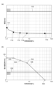
- FIG. 5 is a diagram showing the particle size distribution of the first conductive assistant dispersed in the conductive adhesive layer.
- the horizontal axis indicates the particle size
- the vertical axis indicates the probability of existence (frequency).
- (a) of FIG. 5 shows the particle size distribution of the first conductive assistant contained in the first to fifth samples described below. As can be seen from the shape of the graph 101 shown in (a) of FIG.
- the first conductive assistant is dominated by particles having a particle size of 3.0 ⁇ m or thereabouts, and contains almost no particles having a particle size of less than 2.5 ⁇ m or particles having a particle size of 3.4 ⁇ m or more.
- the average particle size (D50) of the first conductive additive shown in graph 101 is 3 ⁇ m
- the D10 of the first conductive additive is 2.8 ⁇ m
- the D90 of the first conductive additive is 3.2 ⁇ m.
- the standard deviation of the first conductive additive is 0.13 ⁇ m.
- Figure 5(b) is a diagram showing the relationship between the thickness of the conductive adhesive layer and the resistance value of the sample.
- Figure 5(b) shows the measurement results of a 2.5 cm square sample cut from a collector having a first current collecting foil, a second current collecting foil, and a conductive adhesive layer, which will be described below.
- the horizontal axis shows the thickness (film thickness) of the conductive adhesive layer
- the vertical axis shows the resistance values of the first to fifth samples.
- the first sample is a collector in which a 50 ⁇ m thick aluminum foil serving as a first current collecting foil and a 8 ⁇ m thick copper foil serving as a second current collecting foil are integrated by a conductive adhesive layer described below.
- the conductive adhesive layer is a layered member having an adhesive containing an olefin resin as a main component and an epoxy hardener, and a first conductive assistant dispersed in the adhesive, and has a thickness of about 2.2 ⁇ m.
- the amount of the first conductive assistant added was set to 0.2 volume %.
- the second sample is the same as the first sample except that the conductive adhesive layer is about 2.6 ⁇ m thick.
- the third sample is the same as the first sample except that the conductive adhesive layer is about 2.9 ⁇ m thick.
- the fourth sample is the same as the first sample except that the conductive adhesive layer is about 3.2 ⁇ m thick.
- the fifth sample is the same as the first sample except that the conductive adhesive layer is about 3.55 ⁇ m thick.
- line 102 indicates the threshold resistance value.
- Plots 103 to 107 indicate the resistance values of the first to fifth samples, respectively.
- samples showing a resistance value lower than line 102 are electrode current collectors that satisfy the non-defective product conditions for internal resistance.
- only plot 107 showed a resistance value higher than line 102.
- the thickness of the conductive adhesive layer (approximately 3.55 ⁇ m) is clearly larger than the first value (3.26 ⁇ m) obtained by adding twice the standard deviation of the particle size of the first conductive additive (0.13 ⁇ m) to the average particle size of the first conductive additive, and therefore the conduction between the first current collector foil and the second current collector foil via the first conductive additive was insufficient. For this reason, as shown in plots 103 to 106, it is presumed that the first value is greater than the thickness of the conductive adhesive layer, which results in good electrical continuity between the first current collecting foil and the second current collecting foil via the first conductive additive.
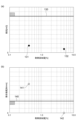
- Figs. 6(a) and 7(a) are diagrams showing the relationship between the additive amount of the conductive additive in the conductive adhesive layer and the internal resistance of the conductive adhesive layer.
- Figs. 6(b) and 7(b) are diagrams showing the relationship between the additive amount of the conductive additive in the conductive adhesive layer and the bonding strength of the conductive adhesive layer. Samples 6 to 10, which will be described below, were used in Figs. 6(a) and 7(b). Samples 11 and 12, which will be described below, were used in Figs. 7(a) and 7(b).
- Samples 6 to 10 are samples with different amounts of the first conductive assistant in the conductive adhesive layer.
- Sample 6 has the same structure and shape as Sample 1, except that the thickness of the conductive adhesive layer is 2.9 ⁇ m and the amount of the first conductive assistant is 0.1 vol.%.
- Sample 7 has the same structure and shape as Sample 6, except that the amount of the first conductive assistant is 0.2 vol.%.
- Sample 8 has the same structure and shape as Sample 6, except that the amount of the first conductive assistant is 0.4 vol.%.
- Sample 9 has the same structure and shape as Sample 6, except that the amount of the first conductive assistant is 0.8 vol.%.
- Sample 10 has the same structure and shape as Sample 6, except that the amount of the first conductive assistant is 5.0 vol.%.
- line 110 indicates the threshold resistance value.
- samples showing resistance values lower than line 110 are electrode collectors that satisfy the quality conditions for internal resistance.
- plots 111 to 115 indicate the resistance values of samples 6 to 10, respectively.
- plot 111 i.e., sample 6
- the resistance value tends to decrease as the proportion of the first conductive additive increases. For this reason, the resistance values of all of samples 7 to 10, which contain a greater amount of the first conductive additive than sample 6, are naturally lower than line 110 (see plots 112 to 115).
- the amount of the first conductive assistant when the amount of the first conductive assistant is more than 0.4 vol.%, the fluctuation in the internal resistance of the conductive adhesive layer is significantly smaller than when the amount of the first conductive assistant is 0.4 vol.% or less.
- the amount of the first conductive assistant in the conductive adhesive layer is less than 0.1 vol.%, the resistance value of the conductive adhesive layer tends to increase rapidly.
- the resistance value of the sample when the amount of the first conductive assistant in the conductive adhesive layer is 0.05 vol.% was near line 110 (not shown). Therefore, when the amount of the first conductive assistant in the conductive adhesive layer is less than 0.1 vol.%, the resistance value of the collector cannot be sufficiently reduced.
- line 120 indicates the threshold value of the bonding strength between the conductive adhesive layer and the current collecting foil contained in the sample.
- a sample showing a bonding strength higher than line 120 is a bipolar electrode current collector that satisfies the good product condition regarding the bonding strength.
- plots 121 to 125 indicate the bonding strength of the sixth to tenth samples, respectively.
- Graph 126 indicates the change in bonding strength with the change in the addition ratio of the first conductive additive.
- Graph 126 is a graph estimated based on plots 121 to 125. As shown in FIG. 6B, all of plots 121 to 124 are higher than line 120, but plot 125 is lower than line 120. Therefore, when an excessive amount of the first conductive additive is contained in the conductive adhesive layer, it can be said that a bipolar electrode current collector that does not satisfy the good product condition regarding the bonding strength is manufactured.
- Sample 11 and Sample 12 are samples with different amounts of conductive assistant in the conductive adhesive layer, and have the same shape as Sample 6.
- the amount of conductive assistant added in Sample 11 is 0.4 volume %, and the amount of conductive assistant added in Sample 12 is 5.0 volume %.
- the conductive assistant (hereinafter referred to as the second conductive assistant) contained in Sample 11 and Sample 12 is different from the first conductive assistant contained in Samples 6 to 10.
- Figure 8 shows the particle size distribution of the second conductive assistant contained in Sample 11 and Sample 12. In Figure 8, the horizontal axis shows the particle size, and the vertical axis shows the probability of existence.
- the average particle size (D50) of the second conductive assistant contained in Sample 11 and Sample 12 and shown in Figure 8 is 2.6 ⁇ m, the D10 of the second conductive assistant is 1.1 ⁇ m, and the D90 of the second conductive assistant is 5.5 ⁇ m.
- the standard deviation of the second conductive assistant is 1.2 ⁇ m.
- line 130 indicates the threshold resistance value.
- samples that show a resistance value lower than line 130 are electrode current collectors that satisfy the quality conditions for internal resistance.
- the threshold value shown by line 130 is the same as the threshold value shown by line 110 shown in FIG. 6A.
- plots 131 and 132 indicate the resistance values of the 11th and 12th samples, respectively.
- plot 131 i.e., the 11th sample
- the resistance value tends to decrease as the addition ratio of the second conductive additive increases. Therefore, the resistance value of plot 132 is naturally lower than line 110 (see plot 132).
- line 140 indicates the threshold value of the bonding strength between the conductive adhesive layer and the current collecting foil contained in the sample.
- the threshold value indicated by line 140 is the same as the threshold value indicated by line 120 shown in FIG. 6B.
- plots 141 and 142 indicate the bonding strength of the 11th and 12th samples, respectively. As shown in FIG. 7B, plot 141 is higher than line 140, but plot 142 is lower than line 140. From this data, it can be said that when the conductive adhesive layer contains an excessive amount of the second conductive additive, a bipolar electrode current collector that does not satisfy the quality conditions for bonding strength is also manufactured.
- the conductive assistant additive ratio in the conductive adhesive layer is 2.0% or less, there is a high possibility that a bipolar electrode collector that satisfies the good product conditions regarding bonding strength can be manufactured, if the additive ratio is 1.0% or less, it can be said that it is possible to reliably manufacture a bipolar electrode collector that satisfies the good product conditions regarding bonding strength, and if the additive ratio is 0.8% or less, it can be said that it is even more possible to reliably manufacture a bipolar electrode collector that satisfies the good product conditions regarding bonding strength.
- the average particle size of the conductive additive 50 may be larger than the thickness TH of the conductive adhesive layer 22. In this case, the electrical continuity between the first current collecting foil 21A and the second current collecting foil 21B via the conductive additive 50 is improved.
- each of the first current collecting foil 21A and the second current collecting foil 21B has a rectangular shape
- the length of one side of the first current collecting foil 21A and the length of one side of the second current collecting foil 21B are each 500 mm or more
- the CV value of the particle size DA of the conductive assistant 50 in the conductive adhesive layer 22 may be 10% or less.
- the conductive assistant 50 having a particle size significantly larger than the thickness TH of the conductive adhesive layer 22 is unlikely to be present in the conductive adhesive layer 22.
- the air present around the conductive assistant 50 is unlikely to be taken into the conductive adhesive layer 22 when the first current collecting foil 21A and the second current collecting foil 21B are bonded together, that is, so-called air entrapment is unlikely to occur. Therefore, an increase in the resistance of the bipolar electrode 14 due to deformation of the first current collecting foil 21A and/or the second current collecting foil 21B caused by the air is unlikely to occur.
- the first current collecting foil 21A and the second current collecting foil 21B can be well bonded to the conductive adhesive layer 22.
- the CV value of the particle size of the first conductive assistant is about 4% (0.13/3 ⁇ 100), which is smaller than 10%.
- the CV value of the particle size of the second conductive assistant is about 46% (1.2/2.6 ⁇ 100), which is significantly larger than 10%.
- each of the first current collecting foil 21A and the second current collecting foil 21B has a rectangular shape, and the length of one side of the first current collecting foil 21A and the length of one side of the second current collecting foil 21B are each 500 mm or more, and the second value obtained by adding the average particle size of the conductive assistant 50 and the standard deviation multiplied by three may be equal to or less than the thickness TH of the conductive adhesive layer 22 multiplied by two. In this case, too, the conductive assistant 50 having a particle size significantly larger than the thickness TH of the conductive adhesive layer 22 is unlikely to be present in the conductive adhesive layer 22.
- the bipolar electrode 14 is enlarged, air is unlikely to be trapped between the first current collecting foil 21A and the second current collecting foil 21B due to the conductive assistant 50. Therefore, an increase in the resistance of the bipolar electrode 14 due to deformation of the first current collecting foil 21A and/or the second current collecting foil 21B caused by the air is unlikely to occur.
- the first current collecting foil 21A and the second current collecting foil 21B can be well bonded to the conductive adhesive layer 22.
- the second value (3.39 ⁇ m) obtained by tripling the average particle size (3 ⁇ m) of the first conductive assistant and the standard deviation (0.13 ⁇ m) of the particle size of the first conductive assistant is smaller than the value (5.8 ⁇ m) obtained by doubling the thickness (2.9 ⁇ m) of the conductive adhesive layer.
- the second value (6.2 ⁇ m) obtained by tripling the average particle size (2.6 ⁇ m) of the second conductive assistant and the standard deviation (1.2 ⁇ m) of the particle size of the second conductive assistant is larger than the value (5.8 ⁇ m) obtained by doubling the thickness (2.9 ⁇ m) of the conductive adhesive layer.
- the thickness of the first current collecting foil 21A is at least twice the thickness of the second current collecting foil 21B, the thickness of the second current collecting foil 21B is less than 10 ⁇ m, the thickness TH of the conductive adhesive layer 22 is smaller than the thickness of the second current collecting foil 21B, and the CV value of the particle size DA of the conductive assistant 50 in the conductive adhesive layer 22 may be 10% or less.
- the conductive assistant 50 having a particle size significantly larger than the thickness TH of the conductive adhesive layer 22 is unlikely to exist in the conductive adhesive layer 22. This makes it difficult for air to be trapped between the first current collecting foil 21A and the second current collecting foil 21B due to the conductive assistant 50.
- the resistance of the bipolar electrode 14 is unlikely to increase due to deformation of the current collecting foil (especially the second current collecting foil 21B) due to the air.
- the resistance of the bipolar electrode 14 is unlikely to increase due to deformation of the current collecting foil (especially the second current collecting foil 21B) due to the air.
- the conductive adhesive layer 22 may further include an epoxy-based curing agent as a curing agent together with the olefin-based adhesive as the adhesive.
- the adhesive can exhibit high electrolyte resistance performance, and therefore good bonding strength can be exhibited for a long period of time.
- an epoxy-based curing agent as a curing agent when an olefin-based adhesive is used as the adhesive, gas generation in the curing reaction between the adhesive and the curing agent that occurs during the manufacture of the current collector 21 can be effectively reduced.
- isocyanate-based curing agents are also generally used as curing agents for olefin-based adhesives, and gas is generated in the curing reaction between the olefin-based adhesive and the isocyanate-based curing agent.
- the conductive adhesive layer 22 may include an epoxy-based curing agent as a curing agent together with the olefin-based adhesive as the adhesive.
- An electricity storage device including a plurality of bipolar electrodes overlapping each other in a stacking direction, Each of the plurality of bipolar electrodes includes: a first current collecting foil and a second current collecting foil overlapping each other in the stacking direction; a conductive adhesive layer located between the first current collecting foil and the second current collecting foil and bonded to the first current collecting foil and the second current collecting foil; a first active material layer located on a surface of the first current collector foil; a second active material layer located on a surface of the second current collector foil; Equipped with The conductive adhesive layer includes an adhesive and a conductive assistant dispersed in the adhesive, the conductive assistant is a spherical particle having a spherical core and a conductive film covering the core, The conductive adhesive layer contains the conductive assistant in an amount of 0.1% by volume or more and 1.0% by
- a first value obtained by adding two times the standard deviation of the particle diameter of the conductive assistant to the average particle diameter of the conductive assistant is equal to or greater than a thickness of the conductive adhesive layer;
- Energy storage device [2] The energy storage device according to [1], wherein an average particle size of the conductive assistant is greater than a thickness of the conductive adhesive layer.
- Each of the first current collecting foil and the second current collecting foil has a rectangular shape, each of a side length of the first current collecting foil and a side length of the second current collecting foil is 500 mm or more;
- the power storage device according to [1] or [2], wherein a CV value of the particle size of the conductive assistant in the conductive adhesive layer is 10% or less.
- Each of the first current collecting foil and the second current collecting foil has a rectangular shape, each of a side length of the first current collecting foil and a side length of the second current collecting foil is 500 mm or more;
- the second value obtained by adding the average particle size of the conductive assistant to three times the standard deviation is equal to or less than twice the thickness of the conductive adhesive layer.
- the thickness of the first current collecting foil is at least twice the thickness of the second current collecting foil, The thickness of the second current collecting foil is less than 10 ⁇ m, the thickness of the conductive adhesive layer is smaller than the thickness of the second current collector foil,
- the power storage device according to any one of [1] to [4], wherein a CV value of the particle size of the conductive assistant in the conductive adhesive layer is 10% or less.
- one aspect of the present disclosure is not limited to the above embodiment and the above [1] to [6].
- One aspect of the present disclosure can be further modified without departing from the spirit of the present disclosure.
- 1...electricity storage device 2...electrode laminate, 3...sealing body, 3a...outer surface, 14...bipolar electrode, 21...current collector, 21A...first current collector foil, 21B...second current collector foil, 21a...first surface, 21b...second surface, 22...conductive adhesive layer, 23...positive electrode active material layer (first active material layer), 24...negative electrode active material layer (second active material layer), 31...spacer, 31a...outer edge, 31b...inner edge, 32...sealing member, 32a...outer edge, 32b...inner edge, 40...adhesive, 50...conductive additive, 51...core, 52...conductive film, D...stacking direction, DA...particle size, T1...sealing member thickness, T2...spacer thickness, TH...conductive adhesive layer thickness.
Landscapes
- Engineering & Computer Science (AREA)
- Power Engineering (AREA)
- Chemical & Material Sciences (AREA)
- Microelectronics & Electronic Packaging (AREA)
- Materials Engineering (AREA)
- Chemical Kinetics & Catalysis (AREA)
- Electrochemistry (AREA)
- General Chemical & Material Sciences (AREA)
- Composite Materials (AREA)
- Manufacturing & Machinery (AREA)
- Cell Electrode Carriers And Collectors (AREA)
Priority Applications (4)
| Application Number | Priority Date | Filing Date | Title |
|---|---|---|---|
| JP2025525987A JPWO2024252821A1 (https=) | 2023-06-08 | 2024-04-25 | |
| CN202480038027.1A CN121263890A (zh) | 2023-06-08 | 2024-04-25 | 蓄电装置 |
| KR1020257041230A KR20260009881A (ko) | 2023-06-08 | 2024-04-25 | 축전 장치 |
| EP24819058.9A EP4700870A1 (en) | 2023-06-08 | 2024-04-25 | Power storage device |
Applications Claiming Priority (2)
| Application Number | Priority Date | Filing Date | Title |
|---|---|---|---|
| JP2023094625 | 2023-06-08 | ||
| JP2023-094625 | 2023-06-08 |
Publications (1)
| Publication Number | Publication Date |
|---|---|
| WO2024252821A1 true WO2024252821A1 (ja) | 2024-12-12 |
Family
ID=93795376
Family Applications (1)
| Application Number | Title | Priority Date | Filing Date |
|---|---|---|---|
| PCT/JP2024/016333 Ceased WO2024252821A1 (ja) | 2023-06-08 | 2024-04-25 | 蓄電装置 |
Country Status (5)
| Country | Link |
|---|---|
| EP (1) | EP4700870A1 (https=) |
| JP (1) | JPWO2024252821A1 (https=) |
| KR (1) | KR20260009881A (https=) |
| CN (1) | CN121263890A (https=) |
| WO (1) | WO2024252821A1 (https=) |
Citations (7)
| Publication number | Priority date | Publication date | Assignee | Title |
|---|---|---|---|---|
| JP2004319210A (ja) | 2003-04-15 | 2004-11-11 | Nissan Motor Co Ltd | バイポーラ電池、バイポーラ電池の製造方法、組電池および車両 |
| JP2005317468A (ja) * | 2004-04-30 | 2005-11-10 | Nissan Motor Co Ltd | バイポーラ電極、バイポーラ電極の製造方法、バイポーラ電池、組電池、およびこれらを搭載した車両 |
| JP2014203625A (ja) * | 2013-04-03 | 2014-10-27 | 株式会社豊田自動織機 | リチウムイオン二次電池正極用集電体、リチウムイオン二次電池用正極及びリチウムイオン二次電池 |
| WO2016031690A1 (ja) * | 2014-08-25 | 2016-03-03 | 日産自動車株式会社 | 電極 |
| JP2020109762A (ja) * | 2015-10-05 | 2020-07-16 | 古河機械金属株式会社 | バイポーラ型リチウムイオン電池およびバイポーラ型リチウムイオン電池の製造方法 |
| JP2020161232A (ja) * | 2019-03-25 | 2020-10-01 | 三洋化成工業株式会社 | リチウムイオン電池 |
| WO2022159985A1 (en) * | 2021-01-25 | 2022-07-28 | Blue Current, Inc. | Solid-state lithium ion multilayer battery and manufacturing method |
-
2024
- 2024-04-25 JP JP2025525987A patent/JPWO2024252821A1/ja active Pending
- 2024-04-25 WO PCT/JP2024/016333 patent/WO2024252821A1/ja not_active Ceased
- 2024-04-25 CN CN202480038027.1A patent/CN121263890A/zh active Pending
- 2024-04-25 EP EP24819058.9A patent/EP4700870A1/en active Pending
- 2024-04-25 KR KR1020257041230A patent/KR20260009881A/ko active Pending
Patent Citations (7)
| Publication number | Priority date | Publication date | Assignee | Title |
|---|---|---|---|---|
| JP2004319210A (ja) | 2003-04-15 | 2004-11-11 | Nissan Motor Co Ltd | バイポーラ電池、バイポーラ電池の製造方法、組電池および車両 |
| JP2005317468A (ja) * | 2004-04-30 | 2005-11-10 | Nissan Motor Co Ltd | バイポーラ電極、バイポーラ電極の製造方法、バイポーラ電池、組電池、およびこれらを搭載した車両 |
| JP2014203625A (ja) * | 2013-04-03 | 2014-10-27 | 株式会社豊田自動織機 | リチウムイオン二次電池正極用集電体、リチウムイオン二次電池用正極及びリチウムイオン二次電池 |
| WO2016031690A1 (ja) * | 2014-08-25 | 2016-03-03 | 日産自動車株式会社 | 電極 |
| JP2020109762A (ja) * | 2015-10-05 | 2020-07-16 | 古河機械金属株式会社 | バイポーラ型リチウムイオン電池およびバイポーラ型リチウムイオン電池の製造方法 |
| JP2020161232A (ja) * | 2019-03-25 | 2020-10-01 | 三洋化成工業株式会社 | リチウムイオン電池 |
| WO2022159985A1 (en) * | 2021-01-25 | 2022-07-28 | Blue Current, Inc. | Solid-state lithium ion multilayer battery and manufacturing method |
Also Published As
| Publication number | Publication date |
|---|---|
| CN121263890A (zh) | 2026-01-02 |
| KR20260009881A (ko) | 2026-01-20 |
| EP4700870A1 (en) | 2026-02-25 |
| JPWO2024252821A1 (https=) | 2024-12-12 |
Similar Documents
| Publication | Publication Date | Title |
|---|---|---|
| US9666858B2 (en) | Negative electrode for secondary battery, and process for production thereof | |
| KR101340133B1 (ko) | 쌍극형 2차 전지 | |
| RU2566741C2 (ru) | Токоотвод для биполярной литий-ионной аккумуляторной батареи | |
| CN102511098B (zh) | 双极型锂离子二次电池用集电体 | |
| JP5470817B2 (ja) | 電池用電極およびこれを用いた電池、並びにその製造方法 | |
| CN102341948B (zh) | 双极型二次电池及其生产方法 | |
| JP5605443B2 (ja) | 非水溶媒双極型二次電池用集電体並びにこれを用いた電極および電池 | |
| US8530084B2 (en) | Electrode structure for non-aqueous electrolyte secondary battery, method for producing the same, and non-aqueous electrolyte secondary battery | |
| US20160043405A1 (en) | Bipolar battery current collector and bipolar battery | |
| JP5418088B2 (ja) | リチウムイオン二次電池用集電体 | |
| JP2010160983A (ja) | 非水電解液二次電池およびその電極 | |
| JP2010160985A (ja) | リチウムイオン二次電池用負極およびこれを用いたリチウムイオン二次電池 | |
| US20160351949A1 (en) | Lithium ion secondary battery | |
| US9099729B2 (en) | Assembled battery and manufacturing method of assembled battery | |
| US20250055101A1 (en) | Power storage device | |
| JP7722249B2 (ja) | 蓄電装置 | |
| WO2024252821A1 (ja) | 蓄電装置 | |
| JP7398231B2 (ja) | 全固体電池システム | |
| CN118985066A (zh) | 蓄电装置 | |
| CN110088967B (zh) | 二次电池 | |
| US20240178364A1 (en) | Battery | |
| JP7489004B2 (ja) | 蓄電セル及び蓄電装置 | |
| US20250253504A1 (en) | Joining method of current collector terminal and current collector tab | |
| US20250286227A1 (en) | Power storage device | |
| US20240097197A1 (en) | Non-aqueous rechargeable battery |
Legal Events
| Date | Code | Title | Description |
|---|---|---|---|
| 121 | Ep: the epo has been informed by wipo that ep was designated in this application |
Ref document number: 24819058 Country of ref document: EP Kind code of ref document: A1 |
|
| ENP | Entry into the national phase |
Ref document number: 2025525987 Country of ref document: JP Kind code of ref document: A |
|
| WWE | Wipo information: entry into national phase |
Ref document number: 2024819058 Country of ref document: EP |
|
| ENP | Entry into the national phase |
Ref document number: 2024819058 Country of ref document: EP Effective date: 20251118 |
|
| ENP | Entry into the national phase |
Ref document number: 2024819058 Country of ref document: EP Effective date: 20251118 |
|
| ENP | Entry into the national phase |
Ref document number: 2024819058 Country of ref document: EP Effective date: 20251118 |
|
| WWE | Wipo information: entry into national phase |
Ref document number: 1020257041230 Country of ref document: KR |
|
| ENP | Entry into the national phase |
Ref document number: 2024819058 Country of ref document: EP Effective date: 20251118 |
|
| ENP | Entry into the national phase |
Ref document number: 2024819058 Country of ref document: EP Effective date: 20251118 |
|
| ENP | Entry into the national phase |
Ref document number: 2024819058 Country of ref document: EP Effective date: 20251118 |
|
| WWE | Wipo information: entry into national phase |
Ref document number: 202617000363 Country of ref document: IN |
|
| ENP | Entry into the national phase |
Ref document number: 2024819058 Country of ref document: EP Effective date: 20251118 |
|
| NENP | Non-entry into the national phase |
Ref country code: DE |
|
| ENP | Entry into the national phase |
Ref document number: 2024819058 Country of ref document: EP Effective date: 20251118 |
|
| WWP | Wipo information: published in national office |
Ref document number: 202617000363 Country of ref document: IN |
|
| ENP | Entry into the national phase |
Ref document number: 2024819058 Country of ref document: EP Effective date: 20251118 |
|
| WWP | Wipo information: published in national office |
Ref document number: 1020257041230 Country of ref document: KR |
|
| WWP | Wipo information: published in national office |
Ref document number: 2024819058 Country of ref document: EP |