WO2024252799A1 - トランジスタおよびその製造方法、並びに集積回路 - Google Patents
トランジスタおよびその製造方法、並びに集積回路 Download PDFInfo
- Publication number
- WO2024252799A1 WO2024252799A1 PCT/JP2024/015405 JP2024015405W WO2024252799A1 WO 2024252799 A1 WO2024252799 A1 WO 2024252799A1 JP 2024015405 W JP2024015405 W JP 2024015405W WO 2024252799 A1 WO2024252799 A1 WO 2024252799A1
- Authority
- WO
- WIPO (PCT)
- Prior art keywords
- thin film
- conductive thin
- top surface
- substrate
- transistor
- Prior art date
- Legal status (The legal status is an assumption and is not a legal conclusion. Google has not performed a legal analysis and makes no representation as to the accuracy of the status listed.)
- Ceased
Links
Images



Classifications
-
- H—ELECTRICITY
- H10—SEMICONDUCTOR DEVICES; ELECTRIC SOLID-STATE DEVICES NOT OTHERWISE PROVIDED FOR
- H10D—INORGANIC ELECTRIC SEMICONDUCTOR DEVICES
- H10D30/00—Field-effect transistors [FET]
- H10D30/60—Insulated-gate field-effect transistors [IGFET]
- H10D30/67—Thin-film transistors [TFT]
- H10D30/674—Thin-film transistors [TFT] characterised by the active materials
- H10D30/675—Group III-V materials, Group II-VI materials, Group IV-VI materials, selenium or tellurium
-
- H—ELECTRICITY
- H10—SEMICONDUCTOR DEVICES; ELECTRIC SOLID-STATE DEVICES NOT OTHERWISE PROVIDED FOR
- H10D—INORGANIC ELECTRIC SEMICONDUCTOR DEVICES
- H10D30/00—Field-effect transistors [FET]
- H10D30/40—FETs having zero-dimensional [0D], one-dimensional [1D] or two-dimensional [2D] charge carrier gas channels
- H10D30/47—FETs having zero-dimensional [0D], one-dimensional [1D] or two-dimensional [2D] charge carrier gas channels having two-dimensional [2D] charge carrier gas channels, e.g. nanoribbon FETs or high electron mobility transistors [HEMT]
- H10D30/471—High electron mobility transistors [HEMT] or high hole mobility transistors [HHMT]
- H10D30/475—High electron mobility transistors [HEMT] or high hole mobility transistors [HHMT] having wider bandgap layer formed on top of lower bandgap active layer, e.g. undoped barrier HEMTs such as i-AlGaN/GaN HEMTs
- H10D30/4755—High electron mobility transistors [HEMT] or high hole mobility transistors [HHMT] having wider bandgap layer formed on top of lower bandgap active layer, e.g. undoped barrier HEMTs such as i-AlGaN/GaN HEMTs having wide bandgap charge-carrier supplying layers, e.g. modulation doped HEMTs such as n-AlGaAs/GaAs HEMTs
-
- H—ELECTRICITY
- H10—SEMICONDUCTOR DEVICES; ELECTRIC SOLID-STATE DEVICES NOT OTHERWISE PROVIDED FOR
- H10D—INORGANIC ELECTRIC SEMICONDUCTOR DEVICES
- H10D30/00—Field-effect transistors [FET]
- H10D30/01—Manufacture or treatment
- H10D30/015—Manufacture or treatment of FETs having heterojunction interface channels or heterojunction gate electrodes, e.g. HEMT
-
- H—ELECTRICITY
- H10—SEMICONDUCTOR DEVICES; ELECTRIC SOLID-STATE DEVICES NOT OTHERWISE PROVIDED FOR
- H10D—INORGANIC ELECTRIC SEMICONDUCTOR DEVICES
- H10D30/00—Field-effect transistors [FET]
- H10D30/01—Manufacture or treatment
- H10D30/017—Manufacture or treatment of FETs having two-dimensional material channels, e.g. TMD FETs
-
- H—ELECTRICITY
- H10—SEMICONDUCTOR DEVICES; ELECTRIC SOLID-STATE DEVICES NOT OTHERWISE PROVIDED FOR
- H10D—INORGANIC ELECTRIC SEMICONDUCTOR DEVICES
- H10D30/00—Field-effect transistors [FET]
- H10D30/01—Manufacture or treatment
- H10D30/021—Manufacture or treatment of FETs having insulated gates [IGFET]
-
- H—ELECTRICITY
- H10—SEMICONDUCTOR DEVICES; ELECTRIC SOLID-STATE DEVICES NOT OTHERWISE PROVIDED FOR
- H10D—INORGANIC ELECTRIC SEMICONDUCTOR DEVICES
- H10D30/00—Field-effect transistors [FET]
- H10D30/40—FETs having zero-dimensional [0D], one-dimensional [1D] or two-dimensional [2D] charge carrier gas channels
- H10D30/47—FETs having zero-dimensional [0D], one-dimensional [1D] or two-dimensional [2D] charge carrier gas channels having two-dimensional [2D] charge carrier gas channels, e.g. nanoribbon FETs or high electron mobility transistors [HEMT]
- H10D30/481—FETs having two-dimensional material channels, e.g. transition metal dichalcogenide [TMD] FETs
- H10D30/485—Vertical FETs having two-dimensional material channels
-
- H—ELECTRICITY
- H10—SEMICONDUCTOR DEVICES; ELECTRIC SOLID-STATE DEVICES NOT OTHERWISE PROVIDED FOR
- H10D—INORGANIC ELECTRIC SEMICONDUCTOR DEVICES
- H10D30/00—Field-effect transistors [FET]
- H10D30/60—Insulated-gate field-effect transistors [IGFET]
- H10D30/67—Thin-film transistors [TFT]
- H10D30/6729—Thin-film transistors [TFT] characterised by the electrodes
- H10D30/673—Thin-film transistors [TFT] characterised by the electrodes characterised by the shapes, relative sizes or dispositions of the gate electrodes
-
- H—ELECTRICITY
- H10—SEMICONDUCTOR DEVICES; ELECTRIC SOLID-STATE DEVICES NOT OTHERWISE PROVIDED FOR
- H10D—INORGANIC ELECTRIC SEMICONDUCTOR DEVICES
- H10D30/00—Field-effect transistors [FET]
- H10D30/60—Insulated-gate field-effect transistors [IGFET]
- H10D30/67—Thin-film transistors [TFT]
- H10D30/6757—Thin-film transistors [TFT] characterised by the structure of the channel, e.g. transverse or longitudinal shape or doping profile
-
- H—ELECTRICITY
- H10—SEMICONDUCTOR DEVICES; ELECTRIC SOLID-STATE DEVICES NOT OTHERWISE PROVIDED FOR
- H10D—INORGANIC ELECTRIC SEMICONDUCTOR DEVICES
- H10D62/00—Semiconductor bodies, or regions thereof, of devices having potential barriers
- H10D62/10—Shapes, relative sizes or dispositions of the regions of the semiconductor bodies; Shapes of the semiconductor bodies
- H10D62/113—Isolations within a component, i.e. internal isolations
-
- H—ELECTRICITY
- H10—SEMICONDUCTOR DEVICES; ELECTRIC SOLID-STATE DEVICES NOT OTHERWISE PROVIDED FOR
- H10D—INORGANIC ELECTRIC SEMICONDUCTOR DEVICES
- H10D62/00—Semiconductor bodies, or regions thereof, of devices having potential barriers
- H10D62/80—Semiconductor bodies, or regions thereof, of devices having potential barriers characterised by the materials
- H10D62/881—Semiconductor bodies, or regions thereof, of devices having potential barriers characterised by the materials being a two-dimensional material
- H10D62/882—Graphene
-
- H—ELECTRICITY
- H10—SEMICONDUCTOR DEVICES; ELECTRIC SOLID-STATE DEVICES NOT OTHERWISE PROVIDED FOR
- H10D—INORGANIC ELECTRIC SEMICONDUCTOR DEVICES
- H10D62/00—Semiconductor bodies, or regions thereof, of devices having potential barriers
- H10D62/80—Semiconductor bodies, or regions thereof, of devices having potential barriers characterised by the materials
- H10D62/881—Semiconductor bodies, or regions thereof, of devices having potential barriers characterised by the materials being a two-dimensional material
- H10D62/883—Transition metal dichalcogenides, e.g. MoSe2
-
- H—ELECTRICITY
- H10—SEMICONDUCTOR DEVICES; ELECTRIC SOLID-STATE DEVICES NOT OTHERWISE PROVIDED FOR
- H10D—INORGANIC ELECTRIC SEMICONDUCTOR DEVICES
- H10D64/00—Electrodes of devices having potential barriers
- H10D64/01—Manufacture or treatment
- H10D64/013—Manufacture or treatment of electrodes having a conductor capacitively coupled to a semiconductor by an insulator
-
- H—ELECTRICITY
- H10—SEMICONDUCTOR DEVICES; ELECTRIC SOLID-STATE DEVICES NOT OTHERWISE PROVIDED FOR
- H10D—INORGANIC ELECTRIC SEMICONDUCTOR DEVICES
- H10D64/00—Electrodes of devices having potential barriers
- H10D64/111—Field plates
-
- H—ELECTRICITY
- H10—SEMICONDUCTOR DEVICES; ELECTRIC SOLID-STATE DEVICES NOT OTHERWISE PROVIDED FOR
- H10D—INORGANIC ELECTRIC SEMICONDUCTOR DEVICES
- H10D64/00—Electrodes of devices having potential barriers
- H10D64/60—Electrodes characterised by their materials
- H10D64/66—Electrodes having a conductor capacitively coupled to a semiconductor by an insulator, e.g. MIS electrodes
-
- H—ELECTRICITY
- H10—SEMICONDUCTOR DEVICES; ELECTRIC SOLID-STATE DEVICES NOT OTHERWISE PROVIDED FOR
- H10D—INORGANIC ELECTRIC SEMICONDUCTOR DEVICES
- H10D84/00—Integrated devices formed in or on semiconductor substrates that comprise only semiconducting layers, e.g. on Si wafers or on GaAs-on-Si wafers
- H10D84/01—Manufacture or treatment
- H10D84/0123—Integrating together multiple components covered by H10D12/00 or H10D30/00, e.g. integrating multiple IGBTs
- H10D84/0126—Integrating together multiple components covered by H10D12/00 or H10D30/00, e.g. integrating multiple IGBTs the components including insulated gates, e.g. IGFETs
-
- H—ELECTRICITY
- H10—SEMICONDUCTOR DEVICES; ELECTRIC SOLID-STATE DEVICES NOT OTHERWISE PROVIDED FOR
- H10D—INORGANIC ELECTRIC SEMICONDUCTOR DEVICES
- H10D84/00—Integrated devices formed in or on semiconductor substrates that comprise only semiconducting layers, e.g. on Si wafers or on GaAs-on-Si wafers
- H10D84/80—Integrated devices formed in or on semiconductor substrates that comprise only semiconducting layers, e.g. on Si wafers or on GaAs-on-Si wafers characterised by the integration of at least one component covered by groups H10D12/00 or H10D30/00, e.g. integration of IGFETs
- H10D84/82—Integrated devices formed in or on semiconductor substrates that comprise only semiconducting layers, e.g. on Si wafers or on GaAs-on-Si wafers characterised by the integration of at least one component covered by groups H10D12/00 or H10D30/00, e.g. integration of IGFETs of only field-effect components
- H10D84/83—Integrated devices formed in or on semiconductor substrates that comprise only semiconducting layers, e.g. on Si wafers or on GaAs-on-Si wafers characterised by the integration of at least one component covered by groups H10D12/00 or H10D30/00, e.g. integration of IGFETs of only field-effect components of only insulated-gate FETs [IGFET]
-
- H—ELECTRICITY
- H10—SEMICONDUCTOR DEVICES; ELECTRIC SOLID-STATE DEVICES NOT OTHERWISE PROVIDED FOR
- H10D—INORGANIC ELECTRIC SEMICONDUCTOR DEVICES
- H10D64/00—Electrodes of devices having potential barriers
- H10D64/20—Electrodes characterised by their shapes, relative sizes or dispositions
- H10D64/23—Electrodes carrying the current to be rectified, amplified, oscillated or switched, e.g. sources, drains, anodes or cathodes
- H10D64/251—Source or drain electrodes for field-effect devices
- H10D64/257—Source or drain electrodes for field-effect devices for lateral devices wherein the source or drain electrodes are characterised by top-view geometrical layouts, e.g. interdigitated, semi-circular, annular or L-shaped electrodes
Definitions
- the present invention relates to a transistor with an extremely short gate length and an extremely thin carrier transport layer, a method for manufacturing the same, and an integrated circuit.
- EUV extreme ultraviolet
- Non-Patent Document 1 In this situation, in response to the demand for extremely short gates and extremely thin carrier transport layers, a transistor having a monoatomic long gate and a channel made of a monoatomic layer of MoS2, which is a two-dimensional semiconductor, has been proposed (see, for example, Non-Patent Document 1).
- Non-Patent Document 1 a graphene film formed on a metal foil by a CVD method is transferred to a substrate, and the transferred graphene is used as a gate.
- a two-dimensional semiconductor is also formed on a metal foil by a CVD method and transferred to a desired substrate.
- the transistor in Non-Patent Document 1 has three major problems. The first problem is that the graphene and two-dimensional semiconductor transferred from the metal foil to the substrate are wrinkled or do not completely adhere to the three-dimensional structure on the substrate surface. Therefore, the device performance value is lower than the theoretical value, and the device reliability is also low. The second problem is that the gate resistance is high.
- the high gate resistance is due to the use of a single layer of graphene as the gate, and prevents the transistor from being made faster.
- the third problem is that in existing device structures suitable for high-frequency applications, some structures and parts such as the gate electrode and insulating layer are shortened or reduced to tens of nanometers or several nanometers, but the device structure and device layout composed of two-dimensional materials and substances with a layer thickness of one to a dozen atoms as in the present invention are not optimized. Due to these issues, transistors with single-atom-long gates have not yet been put to practical use.
- the present invention has been made in consideration of the above, and aims to provide a transistor having a gate with an extremely short length (preferably at the monoatomic level) and a carrier transport layer with an extremely thin thickness (preferably at the monoatomic level), as well as a highly reliable manufacturing method suitable for mass production.
- a transistor includes a substrate having a top surface, a vertical surface intersecting with the top surface and extending downward from the top surface, and a lower surface that is approximately parallel to the top surface and intersects with the vertical surface, a conductive thin film formed in contact with the top surface of the substrate, an insulating film formed so as to cover at least the vertical surface and the end of the conductive thin film, a two-dimensional semiconductor layer formed so as to cover the top surface, the vertical surface, and the lower surface, and formed so as to cover the conductive thin film and/or the insulating film in places where the conductive thin film and/or the insulating film are present, a source electrode provided at a place covering the top surface of the two-dimensional semiconductor layer, and a drain electrode provided at a place covering the lower surface of the two-dimensional semiconductor layer.
- the top surface and/or the lower surface may be flat.
- the transistor may further include a conductor shielding layer on the conductive thin film, and insulating layers may be provided on both the front and back sides of the shielding layer.
- the substrate may have at least the top surface made of single crystal silicon carbide (SiC), and the conductive thin film may be graphene.
- the conductive thin film, graphene may have a single layer at its end that overlaps near the ridge where the top surface intersects with the vertical surface.
- the substrate may have an inclined surface adjacent to the top surface at an end opposite to the edge that contacts the vertical surface of the top surface and that is non-parallel to the top surface, the conductive thin film may be formed from the top surface across the inclined surface, and the conductive thin film on the inclined surface may be multi-layered graphene.
- the substrate may be a single crystal silicon carbide substrate or a hybrid substrate in which a single crystal silicon carbide layer is fabricated on an insulator.
- the two-dimensional semiconductor layer is preferably made of a material selected from the group consisting of graphene, transition metal dichalcogenides, indium oxide, boron phosphide, and boron arsenide.
- the two-dimensional semiconductor layer is particularly preferably made of a transition metal dichalcogenide selected from the group consisting of molybdenum disulfide ( MoS2 ), tungsten disulfide ( WS2 ), and tungsten diselenide ( WSe2 ).
- the insulating film may be formed from a material selected from the group consisting of hafnium oxide, silicon carbide, zirconium oxide, erbium oxide, aluminum oxide, and silicon carbide.
- the method for manufacturing a transistor includes the steps of preparing a substrate, forming a conductive thin film of 10 atomic layers or less on the flat top surface of the substrate, removing the conductive thin film and the upper part of the substrate from other parts while leaving the conductive thin film in a portion by microfabrication to form a vertical surface that intersects with the top surface and extends downward from the top surface, and a lower surface that is approximately parallel to the top surface and intersects with the vertical surface, depositing an insulating film so as to cover at least the vertical surface and the end of the conductive thin film, depositing a two-dimensional semiconductor layer so as to cover the top surface, the vertical surface, and the lower surface, and also to cover the conductive thin film and/or the insulating film in places where the conductive thin film and/or the insulating film are present, and forming a source electrode so as to overlap the part of the two-dimensional semiconductor layer that covers the conductive thin film, and forming a drain electrode so as to overlap the part of
- the present invention after forming the conductive thin film, and before the process of forming the vertical surface and the lower surface, it is preferable to further include a process of providing a shielding layer over the conductive thin film.
- the top surface of the substrate may be a single crystal of silicon carbide, and in the step of forming the conductive thin film, graphene may be formed as a conductive thin film on the top surface of the substrate.
- the conductive thin film is formed from the top surface to the inclined surface, and the conductive thin film on the inclined surface preferably forms multiple layers of graphene.
- the substrate may be a single crystal silicon carbide substrate or a hybrid substrate in which a single crystal silicon carbide layer is fabricated on an insulator.
- the two-dimensional semiconductor layer is preferably made of a material selected from the group consisting of graphene, transition metal dichalcogenides, indium oxide, boron phosphide, and boron arsenide.
- the two-dimensional semiconductor layer is particularly preferably made of a transition metal dichalcogenide selected from the group consisting of molybdenum disulfide ( MoS2 ), tungsten disulfide ( WS2 ), and tungsten diselenide ( WSe2 ).
- the insulating film may be formed from a material selected from the group consisting of hafnium oxide, silicon carbide, zirconium oxide, erbium oxide, aluminum oxide, and silicon carbide.
- transistor suitable for high-frequency applications which has a gate with an extremely short length and a carrier transport layer with an extremely thin thickness. Furthermore, such a transistor can be manufactured with high reliability.
- 1 is a cross-sectional view showing a basic structure of a transistor 1 according to a first embodiment of the present invention.
- 1 is a cross-sectional view showing the structure of an integrated circuit in which a plurality of transistors 1 are formed on a single substrate.
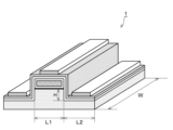
- 1 is a perspective view illustrating a three-dimensional structure of a transistor according to a first embodiment.
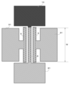
- 2 is a plan view showing an example of a layout in which electrode pads are provided on the transistor 1 according to the first embodiment.
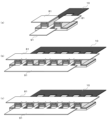
- FIG. FIG. 2 is a schematic diagram of a layout for high output using the transistor 1 according to the first embodiment.
- 2A to 2C are diagrams illustrating an example of a procedure for a method for manufacturing the transistor 1 according to the first embodiment.
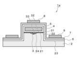
- 1 is a cross-sectional view showing a basic structure of a transistor 1a according to a second embodiment of the present invention.
- Fig. 1 is a cross-sectional view showing a basic structure of a transistor 1 according to a first embodiment of the present invention.
- Fig. 2 is a cross-sectional view showing a structure of an integrated circuit in which a plurality of transistors 1 are formed on one substrate.
- Fig. 3 is a perspective view showing a schematic three-dimensional structure of the transistor 1 according to the first embodiment.
- the transistor 1 includes a substrate 2, a conductive thin film 3, a shielding layer 4, an insulating layer 5, an insulating film 6, a two-dimensional semiconductor layer 7, an electrode 8, and an electrode 9.
- the substrate 2 serves as a base for forming the structure of the transistor 1.
- the substrate 2 is preferably a substrate with a high resistance of at least 10,000 ⁇ or more on at least its surface.
- a material containing silicon carbide may be used as the substrate 2, and at least the top surface 21 may be a single crystal silicon carbide substrate.
- the substrate 2 may be a single crystal silicon carbide substrate, or a hybrid substrate in which a single crystal layer of silicon carbide is formed on an insulator (e.g., single crystal Si, sapphire, etc.).
- a thin film of graphene preferably a monoatomic layer
- the substrate 2 may be made of silicon (Si), sapphire, a quartz glass substrate, a flexible substrate made of a film-like resin such as polyimide or PET (Polyethylene terephthalate), or a transparent conductive oxide such as ITO (Indium Tin Oxide) or FTO (Fluorine-doped Tin Oxide).
- Si silicon
- sapphire a quartz glass substrate
- a flexible substrate made of a film-like resin such as polyimide or PET (Polyethylene terephthalate)
- a transparent conductive oxide such as ITO (Indium Tin Oxide) or FTO (Fluorine-doped Tin Oxide).
- substrate 2 has a top surface 21, a vertical surface 22, and a lower surface 23 formed on one surface.
- Top surface 21 is the uppermost flat surface of substrate 2.
- Vertical surface 22 is a plane that intersects with top surface 21 and extends downward from top surface 21. In the example of FIG. 1, vertical surface 22 and top surface 21 are perpendicular to each other.
- Lower surface 23 intersects with vertical surface 22 and is formed as a plane that is approximately parallel to top surface 21. In the example of FIG. 1, lower surface 23 and vertical surface 22 are perpendicular to each other, and top surface 21 and lower surface 23 are parallel to each other.
- vertical surface 22 is a crystal layer, it is preferable that its surface be a (0001) plane.
- the length from one end to the other end of the top surface 21 (L1 in FIG. 3) and the length from one end to the other end of the lower surface 23 (L2 in FIG. 3) should each be 100 nm to 5 ⁇ m.
- the height of the vertical surface (H in FIG. 3) should be 30 to 100 nm.
- the conductive thin film 3 is an extremely thin conductive thin film of a single atomic layer or several atomic layers (10 atomic layers or less) formed in contact with the top surface 21 of the substrate 2.
- the thickness of the conductive thin film 3 is about several nm (preferably 5 nm) or less.
- the length from one end of the conductive thin film 3 to the other end is preferably about 100 nm to 5 ⁇ m, matching the length L1 of the top surface 21 of the substrate 2.
- a layered conductive material is suitable for the conductive thin film 3. Specifically, graphene, borophene, which is a two-dimensional crystal of boron, and derivatives of borophene are suitable for use.
- graphene can be formed as a single-layer thin film on the (0001) surface of silicon carbide, which is suitable for the substrate 2, and is suitable for the conductive thin film 3.
- titanium nitride (TiN) may be used for the conductive thin film 3.
- the conductive thin film 3 is provided so as to cover the entire top surface 21 of the substrate 2 up to the ridge where the top surface 21 and the vertical surface 22 intersect.
- An end (edge) 31 of the conductive thin film 3 that overlaps the ridge where the top surface 21 and the vertical surface 22 intersect functions as the gate of the transistor 1.
- the portion of the conductive thin film 3 other than the edge 31 functions as wiring from the gate electrode pad 10 to the gate, which will be described later.
- the shielding layer 4 is a layer of a conductor such as a metal provided on the conductive thin film 3, and shields between the electrode 8 and the conductive thin film 3.
- the shielding layer 4 is electrically connected to a predetermined ground potential (e.g., 0 V).
- An insulating layer 5 is provided on at least the front and back sides of the shielding layer 4 to prevent the shielding layer 4 from shorting with the conductive thin film 3 or the electrode 8. It is preferable to use aluminum (Al) or nickel (Ni) as the shielding layer 4.
- Al aluminum
- Ni nickel
- the shielding layer 4 When Ni is used as the shielding layer 4, it is necessary to form a separate insulating layer 5 to prevent shorting with the conductive thin film 3 or the electrode 8. Note that when there is no need to shield between the electrode 8 and the conductive thin film 3 (for example, when signal interference between the electrode 8 and the conductive thin film 3 is not a problem), the transistor 1 does not need to include the shielding layer 4 and the insulating layer 5.
- the end surface 51 of the insulating layer 5 should be a flat surface that is approximately aligned with the vertical surface 22.
- the insulating film 6 is a thin film of an insulator that functions as a gate insulating film of the transistor 1.
- a high dielectric constant insulating film such as hafnium oxide, silicon carbide, zirconium oxide, erbium oxide, aluminum oxide, etc., or a thin film of silicon carbide can be used.
- a thin film of silicon carbide is suitable.
- the insulating film 6 is formed so as to cover the upper surface of the insulating layer 5, the end surface 51, the edge 31, the vertical surface 22, and the lower surface 23.
- the insulating film 6 covers at least the vertical surface 22, the edge 31, and the end surface 51 of the substrate 2, there are cases where it is not necessary to form the insulating film 6 on other parts.
- the insulating film 6 does not need to be provided on the insulating layer 5.
- the substrate 2 has sufficient insulating properties, it is not necessary to provide an insulating film 6 on the lower surface 23.
- the two-dimensional semiconductor layer 7 is a semiconductor layer that functions as a carrier transport layer of the transistor 1.
- the two-dimensional semiconductor layer 7 is formed so as to cover the top surface 21, the vertical surface 22, and the lower surface 23. In places where the conductive thin film 3, the shielding layer 4, the insulating layer 5, and/or the insulating film 6 are present, the two-dimensional semiconductor layer 7 is formed so as to cover them as well.
- transition metal dichalcogenides e.g., molybdenum disulfide (MoS 2 ), tungsten disulfide (WS 2 ), tungsten diselenide (WSe 2 ), etc.
- indium oxide In 2 O 3
- boron phosphide boron arsenide, etc.
- graphene is suitable as the two-dimensional semiconductor layer 7.
- transition metal dichalcogenides such as MoS 2 and WS 2 are suitable for the two-dimensional semiconductor layer 7.
- In 2 O 3 and transition metal dichalcogenides are suitable for the two-dimensional semiconductor layer 7.
- Electrode 8 and electrode 9 are electrodes made of metals such as Au, Al, In, Bi, Ni, Pd, Ti, and Pt, or transparent conductive oxides such as ITO and FTO. Electrode 8 is provided overlapping a portion covering the conductive thin film 3 of the two-dimensional semiconductor layer 7, and functions as the source electrode of the transistor 1. Electrode 9 is provided overlapping a portion covering the lower surface 23 of the two-dimensional semiconductor layer 7, and functions as the drain electrode of the transistor 1.
- transistor 1 having the basic structure described above, the surface on which conductive thin film 3 is formed and the surface on which two-dimensional semiconductor layer 7 covering vertical surface 22 is formed are perpendicular to each other, and edge 31 of conductive thin film 3 faces two-dimensional semiconductor layer 7 via insulating film 6, so the thickness of conductive thin film 3 defines the gate length of transistor 1. If conductive thin film 3 is a monoatomic layer of graphene, the gate length of transistor 1 can be shortened to 0.3 nm. Even if something other than a monoatomic layer of graphene is used for conductive thin film 3, a gate length of several nm or less corresponding to the thickness of conductive thin film 3 can be achieved.
- FIG. 2 is a cross-sectional view showing the structure of an integrated circuit in which multiple transistors 1 are formed on one substrate.
- the above-described transistor 1 structure which has an electrode 8 on the top surface 21 and an electrode 9 on the lower surface 23, and uses the edge 31 of the conductive thin film 3 as a gate, can be formed on both the left and right sides of the convex portion of the substrate 2 on which the top surface 21 is formed, sharing the conductive thin film 3 and the electrode 8, as shown in FIG. 2.
- the transistors 1 can be formed on both the left and right sides of the lower surface 23, sharing the electrode 9.
- an integrated circuit can be formed in which multiple transistors 1 are formed on the substrate 2.
- a larger integrated circuit can be formed by integrating even more transistors 1 (six in the example of FIG. 2).
- FIG. 3 is a perspective view showing a schematic three-dimensional structure of the transistor 1 according to the first embodiment.
- the cross-sectional structure of the transistor 1 shown in FIG. 1 is formed over a desired width W as shown in FIG. 3.
- the width W can be determined arbitrarily depending on the magnitude of the current to be passed through the transistor 1, but from the viewpoint of reliability, the width W is preferably set to about 30 to 50 ⁇ m. For example, if the allowable current per unit width of the channel is 1 A/mm and the width W is 50 ⁇ m, a current of 50 mA can be passed through one transistor 1 structure. If it is desired to pass a larger current, for example, the structure shown in FIG. 2 or the layout shown in FIG. 5 described later can be adopted, and multiple transistor 1 structures can be used in parallel to substantially expand the channel width and achieve the desired allowable current.
- the transistor 1 is provided with a number of electrode pads for connection to the outside.
- a source electrode pad 81 is provided overlapping the electrode 8 and is electrically connected to the electrode 8.
- a drain electrode pad 91 is provided overlapping the electrode 9 and is electrically connected to the electrode 9.
- a gate electrode pad 10 is provided outside the width W and is electrically connected to the conductive thin film 3.
- the source electrode pad 81, the drain electrode pad 91, and the gate electrode pad 10 are each formed with an area sufficient to allow wire bonding or bump formation, and facilitate connection of the source, drain, and gate of the transistor 1 to the outside, respectively.
- an electrode pad for connecting the shielding layer 4 to an external ground potential may be further provided.
- the structure shown in FIG. 4 may be formed in an area of, for example, about 100 ⁇ m square.
- Figures 5(a) to (c) are schematic diagrams of the layout of a transistor 1 for high output.
- Figure 5(a) is a schematic diagram of a layout in which the structure of Figure 1 is provided on both sides of a common drain electrode 9 to increase output.
- Figures 5(b) and (c) show the case in which even more transistors 1 are arranged to achieve even higher output, and the allowable current increases in proportion to the number of transistors arranged, achieving high output.
- the number of transistors 1 that operate and form a current path (channel layer) can be determined arbitrarily. Comparing the configuration of FIG. 5(b), in which the comb electrodes are thinned out, with the configuration of FIG. 5(c), in which comb electrodes are provided on all electrodes 9, the configuration of FIG. 5(c) forms twice as many current paths (channel layers), doubles the current value and mutual conductance (gm), and enables higher output. Note that electrodes 9 do not need to be provided in the locations where the comb electrodes are thinned out in FIG. 5(b).
- a method for manufacturing a transistor 1 having a structure in which a single layer of graphene is provided on a silicon carbide substrate will be described as an example of the transistor 1 according to this embodiment.
- a substrate 2 having a silicon carbide (0001) surface on the upper surface is prepared (FIG. 6(a)).
- a single graphene layer that will become the conductive thin film 3 is formed on the upper surface of the substrate 2 (FIG. 6(b)).
- the graphene layer can be graphened by thermal sublimation of Si atoms, chemical vapor deposition, molecular beam epitaxy, or the like.
- an Al shielding layer 4 is formed on the conductive thin film 3.
- an insulating layer 5 of a natural oxide film is formed on the shielding layer 4 so as to cover its surface (FIG. 6(c)).
- microfabrication is performed by reactive ion etching or neutral particle beam etching using a chlorine-based gas or a fluorine-based gas, thereby digging down a part of the substrate 2 to form a vertical surface 22 and a lower surface 23 on the substrate 2, and the shielding layer 4 is processed to match the vertical surface 22 (FIG. 6(d)).
- the side of the shielding layer 4 is exposed during the microfabrication process, and an insulating layer 5 of a natural oxide film is formed again to cover the exposed surface.
- an insulating film 6 is deposited (FIG. 6(e)).
- the insulating film 6 is formed so as to cover the upper surface of the insulating layer 5, the end surface 51, the edge 31, the vertical surface 22, and the lower surface 23. Note that as long as the insulating film 6 covers at least the vertical surface 22, the edge 31, and the end surface 51 of the substrate 2, it may not be necessary to form the insulating film 6 on other parts.
- the two-dimensional semiconductor layer 7 is deposited so as to cover the top surface 21, the vertical surface 22, and the lower surface 23 (FIG. 6(f)).
- the two-dimensional semiconductor layer 7 is formed so as to cover the conductive thin film 3, the shielding layer 4, the insulating layer 5, and/or the insulating film 6 in places where they are present.
- an electrode 8 is formed so as to cover the conductive thin film 3 in the two-dimensional semiconductor layer 7, and an electrode 9 is formed so as to cover the lower surface 23 in the two-dimensional semiconductor layer 7 (FIG. 6(g)).
- the basic structure of the transistor 1 is completed as described above at 41.
- a device that can be connected to the outside can be obtained by providing a source electrode pad 81, a drain electrode pad 91, and a gate electrode pad 10 to the electrode 8, the electrode 9, and the conductive thin film 3, respectively.
- the transistor 1 described above can achieve a gate length of a single atom (approximately 0.3 nm), enabling a speed that exceeds that of the currently fastest high electron mobility transistor (InGaAs-HEMT) with a channel made of a compound semiconductor made of InGaAs. Furthermore, even if the conductive thin film is a few atomic layers thick (for example, approximately 1 nm thick), it is possible to achieve a shorter gate length and higher speed than current transistors, which are approaching the limits of exposure equipment.
- the conductive thin film 3 and the two-dimensional semiconductor layer 7 are not transferred from another substrate, but are grown directly on the top surface 21 and the insulating film 6, so they do not wrinkle and can be perfectly adhered to the three-dimensional structure of the substrate surface.
- the transistor 1 according to this embodiment can use a two-dimensional semiconductor with a band gap about three times larger than that of InGaAs for the two-dimensional semiconductor layer 7, enabling high output performance that exceeds that of InGaAs-HEMTs by more than an order of magnitude.
- the transistor 1 according to this embodiment can use Si with a silicon carbide thin film, silicon carbide, sapphire with a silicon carbide thin film, etc. as the substrate 2, allowing for a high degree of freedom in substrate selection. This allows for applications not only to ultra-high frequency devices, but also to large scale logic integrated circuits.
- a transistor 1a according to a second embodiment of the present invention will be described with reference to FIG. 7.
- the gate resistance becomes high due to its extremely thin thickness.
- the edge of the single layer of graphene is used as the gate electrode, and the graphene in the portion other than the vicinity of the edge is multi-layered to suppress the gate resistance.
- the feature of this embodiment is the configuration for multi-layering the graphene in the portion other than the vicinity of the edge in the first embodiment. Note that the rest is the same as the first embodiment described above, so the description here will be omitted.
- FIG. 7 is a cross-sectional view showing a basic structure of a transistor 1a according to the second embodiment.
- the transistor 1a includes a substrate 2, a conductive thin film 3, a shielding layer 4, an insulating layer 5, an insulating film 6, a two-dimensional semiconductor layer 7, an electrode 8, and an electrode 9, similar to the transistor 1 according to the first embodiment.
- the substrate 2 used in the transistor 1a has a slope 24 in addition to a top surface 21, a vertical surface 22, and a lower surface 23. In the substrate 2, at least the top surface 21 and the slope 24 are single crystals of silicon carbide.
- the top surface 21 is preferably a (0001) surface of silicon carbide.
- the slope 24 is a surface that is non-parallel (inclined) to the top surface 21 and is provided adjacent to the top surface 21 at the end opposite to the edge of the top surface 21 that contacts the vertical surface 22.
- the slope angle of the slope 24 is arbitrary, but may be, for example, 45°, 22°, etc.
- the inclined surface 24 having such an inclination angle can be formed by appropriately adjusting the gas flow rate and the high frequency power (for example, a gas flow rate of 40 sccm and a high frequency power of 50 W) in reactive ion etching using Cl 2.
- the inclination angle of the inclined surface 24 does not need to be constant, and may be formed as a curved surface, for example. Such an inclined surface 24 is provided prior to the formation of the conductive thin film 3.
- the conductive thin film 3 is simultaneously formed from the top surface 21 to the inclined surface 24. Since the growth rate of graphene on the inclined surface 24 is faster than the growth rate of graphene on the top surface 21, which is the (0001) surface of silicon carbide, multiple layers of graphene (preferably about 10 to 20 layers) grow on the inclined surface 24 while a single layer of graphene grows on the top surface 21. Therefore, the conductive thin film 3 in this embodiment is formed from the top surface 21 to the slope 24, and has a structure in which the vicinity of the edge 31 is made of single-layer graphene 32 and the vicinity of the inner slope 24 is made of multi-layer graphene 33.
- the distance from the ridge line where the top surface 21 and the vertical surface 22 of the substrate 2 intersect to the slope 24 should be a distance sufficient to prevent the formation of multi-layer graphene from extending to the vicinity of the edge 31 (for example, about several hundreds of nm).
- Transistor 1a is constructed by providing a conductive thin film 3 as described above with a shielding layer 4, insulating layer 5, insulating film 6, two-dimensional semiconductor layer 7, electrode 8, and electrode 9 similar to those in the first embodiment. Note that a recess will be formed in the conductive thin film 3 due to the inclination of the underlying slope 24, but it is advisable to fill this recess with an insulating material or the like to form a flat surface before stacking the shielding layer 4, insulating film 6, two-dimensional semiconductor layer 7, etc.
- the carrier density increases due to the multi-layering of the graphene that constitutes the conductive thin film 3, so that the resistance of the conductive thin film 3 as a whole can be reduced.
- a single layer of graphene faces the two-dimensional semiconductor layer 7 via the insulating film 6 and functions as a gate electrode, so that the gate length of the transistor 1 can be one atom (about 0.3 nm).
- Reference Signs List 1 1a Transistor 2 Substrate 21 Top surface 22 Vertical surface 23 Lower surface 24 Slope 3 Conductive thin film 31 Edge 32 Single-layer graphene 33 Multi-layer graphene 4 Shielding layer 5 Insulating layer 51 End surface 6 Insulating film 7 Two-dimensional semiconductor layer 8, 9 Electrode 81 Source electrode pad 91 Drain electrode pad 10 Gate electrode pad
Landscapes
- Thin Film Transistor (AREA)
Abstract
Description
図1は、本発明の第1実施形態に係るトランジスタ1の基本構造を示す断面図である。図2は、1つの基板上に複数のトランジスタ1が形成された集積回路の構造を示す断面図である。図3は、第1実施形態に係るトランジスタ1の立体構造を模式的に示す斜視図である。図1に示すように、トランジスタ1は、基板2、導電薄膜3、遮蔽層4、絶縁層5、絶縁膜6、二次元半導体層7、電極8、および電極9を備える。
続いて、図7を参照して、本発明の第2実施形態に係るトランジスタ1aを説明する。ゲート抵抗が高いとトランジスタの高周波特性は抑制されてしまうところ、第1実施形態の構造のトランジスタ1において導電薄膜3に単層のグラフェンを採用する場合、その極めて薄い厚みによりゲート抵抗が高くなってしまう。本実施形態に係るトランジスタ1aでは、ゲート電極として単層のグラフェンのエッジを利用しつつ、エッジの近傍以外の部分のグラフェンを多層化することによりゲート抵抗を抑制する。本実施形態の特徴は、第1実施形態におけるエッジの近傍以外の部分のグラフェンを多層化するための構成にある。なお、それ以外については、上述した第1の実施形態と同様なので、ここでの説明を省略する。
2 基板
21 最上面
22 垂直面
23 下段面
24 斜面
3 導電薄膜
31 エッジ
32 単層グラフェン
33 多層グラフェン
4 遮蔽層
5 絶縁層
51 端面
6 絶縁膜
7 二次元半導体層
8,9 電極
81 ソース電極パッド
91 ドレイン電極パッド
10 ゲート電極パッド
Claims (20)
- 最上面と、前記最上面と交わり前記最上面より下方に延びる垂直面と、前記最上面と略平行であり前記垂直面と交わる下段面とを有する基板と、
前記基板の前記最上面に接して形成される導電薄膜と、
少なくとも、前記垂直面、前記導電薄膜の端部を覆うように形成される絶縁膜と、
前記最上面、前記垂直面、および前記下段面を覆うように形成される二次元半導体層であって、前記導電薄膜および/または前記絶縁膜が存在する箇所については前記導電薄膜および/または前記絶縁膜をも覆うように重ねて形成される、二次元半導体層と、
前記二次元半導体層における前記最上面を覆う箇所に設けられるソース電極と、
前記二次元半導体層における前記下段面を覆う箇所に設けられるドレイン電極と、
を備えるトランジスタ。 - 前記導電薄膜の上に、導体の遮蔽層をさらに備え、
前記遮蔽層の表裏両面に絶縁層が設けられる
ことを特徴とする請求項1に記載のトランジスタ。 - 前記基板は、少なくとも前記最上面が炭化珪素の単結晶であり、
前記導電薄膜は、グラフェンであることを特徴とする請求項1または2に記載のトランジスタ。 - 前記導電薄膜であるグラフェンは、前記最上面と前記垂直面が交わる稜線近傍に重なる端部が単層であることを特徴とする請求項3に記載のトランジスタ。
- 前記基板は、前記最上面の前記垂直面と接する縁とは反対の端部において前記最上面に隣接し前記最上面と非平行である傾斜面を備え、
前記導電薄膜は前記最上面から前記傾斜面に渡って形成され、
前記傾斜面の上における前記導電薄膜は多層のグラフェンである
ことを特徴とする請求項4に記載のトランジスタ。 - 前記基板は、炭化珪素の単結晶基板または絶縁体に炭化珪素の単結晶層を作製したハイブリッド基板であることを特徴とする請求項1または2に記載のトランジスタ。
- 前記二次元半導体層は、グラフェン、遷移金属ダイカルコゲナイド、酸化インジウム、リン化ホウ素、および砒化ホウ素からなる群から選択される材料により形成されることを特徴とする請求項1または2に記載のトランジスタ。
- 前記二次元半導体層は、二硫化モリブデン(MoS2)、二硫化タングステン(WS2)、および二セレン化タングステン(WSe2)のいずれかである遷移金属ダイカルコゲナイドより形成されることを特徴とする請求項7に記載のトランジスタ。
- 前記絶縁膜は、酸化ハフニウム、炭化珪素、酸化ジルコニウム、酸化エルビウム、酸化アルミニウム、および炭化珪素からなる群から選択される材料により形成されることを特徴とする請求項1または2に記載のトランジスタ。
- 請求項1または2に記載のトランジスタを複数備える集積回路であって、
前記基板は、前記最上面が形成された凸部に対向する2つの前記垂直面を有し、
1つの前記導電薄膜および1つの前記ソース電極を2つの前記トランジスタが共用することを特徴とする集積回路。 - 請求項1または2に記載のトランジスタを複数備える集積回路であって、
前記基板は、1つの前記下段面の両側に対向する2つの前記垂直面を有し、
1つの前記下段面を2つの前記トランジスタが共用することを特徴とする集積回路。 - 基板を準備する工程と、
前記基板の平坦な最上面に10原子層以下の導電薄膜を形成する工程と、
微細加工により、一部に前記導電薄膜を残しつつ、他の部分について前記導電薄膜および前記基板の上部を除去して、前記基板に、前記最上面と交わり前記最上面より下方に延びる垂直面と、前記最上面と略平行であり前記垂直面と交わる下段面垂直面および下段面とを形成する工程と、
少なくとも、前記垂直面、前記導電薄膜の端部を覆うように絶縁膜を堆積する工程と、
前記最上面、前記垂直面、および前記下段面を覆うように、且つ、前記導電薄膜および/または前記絶縁膜が存在する箇所については前記導電薄膜および/または前記絶縁膜をも覆うように重ねて二次元半導体層を堆積する工程と、
前記二次元半導体層における前記導電薄膜を覆う箇所に重ねてソース電極を形成し、前記二次元半導体層における前記下段面を覆う箇所に重ねてドレイン電極を形成する工程と
を備えるトランジスタの製造方法。 - 前記導電薄膜を形成した後、前記垂直面および前記下段面を形成する工程の前に、前記導電薄膜に重ねて遮蔽層を設ける工程をさらに備えることを特徴とする請求項12に記載の製造方法。
- 前記基板は、少なくとも前記最上面が炭化珪素の単結晶であり、
前記導電薄膜を形成する工程において、前記基板の前記最上面に前記導電薄膜としてグラフェンを形成することを特徴とする請求項12または13に記載の製造方法。 - 前記導電薄膜を形成する工程において、前記導電薄膜であるグラフェンを、前記最上面と前記垂直面が交わる稜線近傍に重なる端部が単層となるように形成すること特徴とする請求項12または13に記載の製造方法。
- 前記導電薄膜を形成する工程より前に、前記最上面に隣接し前記最上面と非平行である傾斜面を形成する工程を有し、
前記導電薄膜を形成する工程において、前記導電薄膜を前記最上面から前記傾斜面に渡って形成し、前記傾斜面の上における前記導電薄膜は多層のグラフェンを形成することを特徴とする請求項15に記載の製造方法。 - 前記基板は、炭化珪素の単結晶基板または絶縁体に炭化珪素の単結晶層を作製したハイブリッド基板であることを特徴とする請求項12または13に記載の製造方法。
- 前記二次元半導体層は、グラフェン、遷移金属ダイカルコゲナイド、酸化インジウム、リン化ホウ素、および砒化ホウ素からなる群から選択される材料により形成されることを特徴とする請求項12または13に記載の製造方法。
- 前記二次元半導体層は、二硫化モリブデン(MoS2)、二硫化タングステン(WS2)、および二セレン化タングステン(WSe2)のいずれかである遷移金属ダイカルコゲナイドより形成されることを特徴とする請求項18に記載の製造方法。
- 前記絶縁膜は、酸化ハフニウム、炭化珪素、酸化ジルコニウム、酸化エルビウム、酸化アルミニウム、および炭化珪素からなる群から選択される材料により形成されることを特徴とする請求項12または13に記載の製造方法。
Priority Applications (3)
| Application Number | Priority Date | Filing Date | Title |
|---|---|---|---|
| KR1020257040613A KR20260020106A (ko) | 2023-06-09 | 2024-04-18 | 트랜지스터 및 그 제조 방법, 그리고 집적 회로 |
| CN202480037780.9A CN121312277A (zh) | 2023-06-09 | 2024-04-18 | 晶体管及其制造方法、以及集成电路 |
| EP24819037.3A EP4726782A1 (en) | 2023-06-09 | 2024-04-18 | Transistor, method for manufacturing same, and integrated circuit |
Applications Claiming Priority (2)
| Application Number | Priority Date | Filing Date | Title |
|---|---|---|---|
| JP2023-095711 | 2023-06-09 | ||
| JP2023095711A JP2024176868A (ja) | 2023-06-09 | 2023-06-09 | トランジスタおよびその製造方法、並びに集積回路 |
Publications (1)
| Publication Number | Publication Date |
|---|---|
| WO2024252799A1 true WO2024252799A1 (ja) | 2024-12-12 |
Family
ID=93795355
Family Applications (1)
| Application Number | Title | Priority Date | Filing Date |
|---|---|---|---|
| PCT/JP2024/015405 Ceased WO2024252799A1 (ja) | 2023-06-09 | 2024-04-18 | トランジスタおよびその製造方法、並びに集積回路 |
Country Status (6)
| Country | Link |
|---|---|
| EP (1) | EP4726782A1 (ja) |
| JP (1) | JP2024176868A (ja) |
| KR (1) | KR20260020106A (ja) |
| CN (1) | CN121312277A (ja) |
| TW (1) | TW202450131A (ja) |
| WO (1) | WO2024252799A1 (ja) |
Citations (3)
| Publication number | Priority date | Publication date | Assignee | Title |
|---|---|---|---|---|
| JP2016219805A (ja) * | 2015-05-18 | 2016-12-22 | 三星電子株式会社Samsung Electronics Co.,Ltd. | 二次元物質を含む半導体素子及びその製造方法 |
| US20200044083A1 (en) * | 2018-08-05 | 2020-02-06 | International Business Machines Corporation | Vertical Transistor with One Atomic Layer Gate Length |
| US20210327758A1 (en) * | 2018-08-23 | 2021-10-21 | Massachusetts Institute Of Technology | Atomic precision control of wafer-scale two-dimensional materials |
-
2023
- 2023-06-09 JP JP2023095711A patent/JP2024176868A/ja active Pending
-
2024
- 2024-04-18 WO PCT/JP2024/015405 patent/WO2024252799A1/ja not_active Ceased
- 2024-04-18 EP EP24819037.3A patent/EP4726782A1/en active Pending
- 2024-04-18 CN CN202480037780.9A patent/CN121312277A/zh active Pending
- 2024-04-18 KR KR1020257040613A patent/KR20260020106A/ko active Pending
- 2024-06-06 TW TW113121068A patent/TW202450131A/zh unknown
Patent Citations (3)
| Publication number | Priority date | Publication date | Assignee | Title |
|---|---|---|---|---|
| JP2016219805A (ja) * | 2015-05-18 | 2016-12-22 | 三星電子株式会社Samsung Electronics Co.,Ltd. | 二次元物質を含む半導体素子及びその製造方法 |
| US20200044083A1 (en) * | 2018-08-05 | 2020-02-06 | International Business Machines Corporation | Vertical Transistor with One Atomic Layer Gate Length |
| US20210327758A1 (en) * | 2018-08-23 | 2021-10-21 | Massachusetts Institute Of Technology | Atomic precision control of wafer-scale two-dimensional materials |
Non-Patent Citations (2)
| Title |
|---|
| FAN WU ET AL., NATURE, vol. 603, 2022, pages 259 |
| FAN, WU ET AL.: "Vertical MoS2 transistors with sub-1-nm gate lengths", NATURE, vol. 603, no. 7900, 2022, pages 259 - 264, XP037712043, DOI: 10.1038/s41586-021-04323-3 * |
Also Published As
| Publication number | Publication date |
|---|---|
| JP2024176868A (ja) | 2024-12-19 |
| TW202450131A (zh) | 2024-12-16 |
| CN121312277A (zh) | 2026-01-09 |
| EP4726782A1 (en) | 2026-04-15 |
| KR20260020106A (ko) | 2026-02-10 |
Similar Documents
| Publication | Publication Date | Title |
|---|---|---|
| KR101419631B1 (ko) | 그래핀 채널 기반의 디바이스와 그의 제조방법 | |
| US12142697B2 (en) | Two-dimensional material-based wiring conductive layer contact structures, electronic devices including the same, and methods of manufacturing the electronic devices | |
| TWI799936B (zh) | 半導體裝置及形成半導體裝置之方法 | |
| US8455297B1 (en) | Method to fabricate high performance carbon nanotube transistor integrated circuits by three-dimensional integration technology | |
| JP7032071B2 (ja) | トランジスタ | |
| TWI786872B (zh) | 積體電路及其製造方法 | |
| TWI616989B (zh) | 用於結合石墨烯的氟化石墨烯絕緣體和裝置 | |
| US11133410B2 (en) | Field-effect transistors and methods of manufacturing the same | |
| TWI784950B (zh) | 間斷帶隙接點 | |
| CN116472612A (zh) | 量子比特电路、量子计算机以及量子比特电路的制造方法 | |
| CN109712961B (zh) | 三维集成电路及其制造方法 | |
| JP2024176868A (ja) | トランジスタおよびその製造方法、並びに集積回路 | |
| US8368053B2 (en) | Multilayer-interconnection first integration scheme for graphene and carbon nanotube transistor based integration | |
| US11063118B1 (en) | TeraHertz capable integrated circuit | |
| US12062712B2 (en) | Terahertz capable integrated circuit | |
| EP4726781A1 (en) | Integrated circuit and method for manufacturing same |
Legal Events
| Date | Code | Title | Description |
|---|---|---|---|
| 121 | Ep: the epo has been informed by wipo that ep was designated in this application |
Ref document number: 24819037 Country of ref document: EP Kind code of ref document: A1 |
|
| WWE | Wipo information: entry into national phase |
Ref document number: 2024819037 Country of ref document: EP |
|
| NENP | Non-entry into the national phase |
Ref country code: DE |
|
| ENP | Entry into the national phase |
Ref document number: 2024819037 Country of ref document: EP Effective date: 20260109 |
|
| ENP | Entry into the national phase |
Ref document number: 2024819037 Country of ref document: EP Effective date: 20260109 |
|
| ENP | Entry into the national phase |
Ref document number: 2024819037 Country of ref document: EP Effective date: 20260109 |
|
| WWP | Wipo information: published in national office |
Ref document number: 2024819037 Country of ref document: EP |