WO2024252778A1 - フィルムコンデンサ - Google Patents
フィルムコンデンサ Download PDFInfo
- Publication number
- WO2024252778A1 WO2024252778A1 PCT/JP2024/014120 JP2024014120W WO2024252778A1 WO 2024252778 A1 WO2024252778 A1 WO 2024252778A1 JP 2024014120 W JP2024014120 W JP 2024014120W WO 2024252778 A1 WO2024252778 A1 WO 2024252778A1
- Authority
- WO
- WIPO (PCT)
- Prior art keywords
- film
- protective film
- internal electrode
- electrode layer
- organic material
- Prior art date
- Legal status (The legal status is an assumption and is not a legal conclusion. Google has not performed a legal analysis and makes no representation as to the accuracy of the status listed.)
- Ceased
Links
Images


Classifications
-
- H—ELECTRICITY
- H01—ELECTRIC ELEMENTS
- H01G—CAPACITORS; CAPACITORS, RECTIFIERS, DETECTORS, SWITCHING DEVICES, LIGHT-SENSITIVE OR TEMPERATURE-SENSITIVE DEVICES OF THE ELECTROLYTIC TYPE
- H01G4/00—Fixed capacitors; Processes of their manufacture
- H01G4/002—Details
- H01G4/224—Housing; Encapsulation
-
- H—ELECTRICITY
- H01—ELECTRIC ELEMENTS
- H01G—CAPACITORS; CAPACITORS, RECTIFIERS, DETECTORS, SWITCHING DEVICES, LIGHT-SENSITIVE OR TEMPERATURE-SENSITIVE DEVICES OF THE ELECTROLYTIC TYPE
- H01G4/00—Fixed capacitors; Processes of their manufacture
- H01G4/32—Wound capacitors
Definitions
- the present invention relates to a film capacitor.
- One type of capacitor is a film capacitor, which is made of a wound or laminated dielectric film with an internal electrode layer made of a metal vapor deposition film on its surface.
- a metallized film with an internal electrode layer formed on the surface of a dielectric film is rolled or laminated to produce a laminate, and then a protective film to protect the metallized film may be rolled onto the outermost layer of the laminate.
- thermoplastic resins such as polypropylene are often used as materials for protective films.
- Film capacitors used in applications such as vehicle inverter smoothing capacitors are often subjected to high temperature and long-term voltage application. This causes the internal electrode layer, which is a vapor-deposited electrode, to gradually oxidize, resulting in problems such as an increase in the equivalent series resistance of the film capacitor and a decrease in capacitance.
- the present invention has been made to solve the above problems, and aims to provide a film capacitor that can suppress oxidation of the internal electrode layer even when voltage is applied for long periods at high temperatures.
- the film capacitor of the present invention comprises a laminate in which a dielectric film and an internal electrode layer are wound or laminated, and a protective film that covers the outer peripheral surface of the laminate in the lamination direction of the laminate, the protective film being made of a thermosetting urethane resin and containing unreacted isocyanate groups.
- the present invention provides a film capacitor that can suppress oxidation of the internal electrode layer even when voltage is applied for a long period of time at high temperatures.
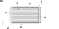
- FIG. 1 is a cross-sectional view illustrating an example of a film capacitor according to the present invention.
- FIG. 2 is a perspective view illustrating an example of a laminate.
- FIG. 3 is a perspective view that illustrates an example of a protective film that covers the outer peripheral surface of the laminate.
- FIG. 4 is a graph showing the ESR increase rate in the film capacitors of the examples and the comparative example.
- FIG. 5 is a graph showing the infrared absorption spectrum of the protective film used in the film capacitor of the example.
- the film capacitor of the present invention will be described below. However, the present invention is not limited to the following configurations, and can be appropriately modified and applied within the scope of the present invention.
- the present invention also includes a combination of two or more of the individual preferred configurations of the present invention described below.
- terms indicating the relationship between elements e.g., "perpendicular,” “parallel,” “orthogonal,” etc.
- terms indicating the shapes of elements are not expressions that express only a strict meaning, but are expressions that include a range of substantial equivalence, for example, differences of about a few percent.
- the film capacitor of the present invention is characterized in that the protective film covering the outer surface of the laminate is made of a thermosetting urethane resin and contains unreacted isocyanate groups.
- the film capacitor of the present invention by using a film made of a thermosetting urethane resin containing unreacted isocyanate groups as a protective film, it is possible to suppress oxidation of the internal electrode layer even when voltage is applied for a long period of time at high temperatures.
- the reason for this is presumably that the unreacted isocyanate groups react with moisture in the usage environment of the film capacitor first and are consumed, suppressing oxidation of the internal electrode layer due to moisture.
- the equivalent series resistance of the film capacitor is unlikely to increase and the electrostatic capacitance is unlikely to decrease. In this way, a film capacitor with excellent high-temperature resistance can be obtained.
- the presence of unreacted isocyanate groups in the protective film can be confirmed by Fourier transform infrared absorption spectroscopy (FT-IR) analysis.
- FT-IR Fourier transform infrared absorption spectroscopy
- the method for producing a protective film made of a thermosetting urethane resin containing unreacted isocyanate groups is not particularly limited, and examples include a method of blending an excess of an isocyanate compound in advance, and a method of adjusting the heat treatment conditions (temperature, time, etc.).
- the peak intensity ratio of isocyanate group/carbonyl group calculated as the ratio of the absorption peak intensity of isocyanate group detected in the wave number range of 2200 cm -1 to 2350 cm -1 to the absorption peak intensity of carbonyl group detected in the wave number range of 1650 cm -1 to 1800 cm -1 , is preferably 0.1 to 1.7.
- the peak intensity ratio of isocyanate groups/carbonyl groups in the protective film shows a positive correlation with the content of unreacted isocyanate groups contained in the protective film.
- the peak intensity ratio of isocyanate groups/carbonyl groups is 0.1 or more.
- the above peak intensity ratio may be 0.2 or more, 0.3 or more, 0.4 or more, 0.5 or more, or 0.6 or more.
- the peak intensity ratio of isocyanate groups/carbonyl groups is 1.7 or less.
- the above peak intensity ratio may be 1.6 or less, 1.5 or less, 1.4 or less, 1.3 or less, 1.2 or less, 1.1 or less, or 1.0 or less.
- the absorption peak intensity means a value calculated as follows:
- the infrared absorption spectrum of the protective film is measured by attenuated total reflection (ATR) using a Fourier transform infrared spectrophotometer (FT-IR).
- ATR attenuated total reflection
- FT-IR Fourier transform infrared spectrophotometer
- the absorption band observed in a specified wave number region is determined to be due to a specified functional group, and a baseline is drawn on both sides of each peak. The value from the baseline to the peak intensity is determined as the "absorption peak intensity" of that functional group.
- a metal layer may be provided on at least one surface of the protective film. If a metal layer is provided on the surface of the protective film, the barrier properties against moisture can be improved.
- metals contained in the metal layer include aluminum (Al), titanium (Ti), zinc (Zn), magnesium (Mg), tin (Sn), and nickel (Ni).
- the metal layer may contain one type of metal, or two or more types of metals.
- the metal layer may contain an alloy.
- the metal layer may be the same as the metal contained in the internal electrode layer, or may be different.
- the thickness of the metal layer is not particularly limited, but is, for example, 5 nm or more and 40 nm or less.
- the thickness of the metal layer may be the same as the thickness of the internal electrode layer, may be greater than the thickness of the internal electrode layer, or may be smaller than the thickness of the internal electrode layer.
- the thickness of the metal layer can be determined by observing a cross section of the protective film on which the metal layer is provided, cut in the thickness direction, using an electron microscope such as a field emission scanning electron microscope (FE-SEM).
- FE-SEM field emission scanning electron microscope
- the protective film is preferably wrapped around the outer peripheral surface of the laminate.
- the number of times the protective film is wrapped is not particularly limited, and the protective film may be wrapped around the outer peripheral surface of the laminate one revolution, or the protective film may be wrapped around the outer peripheral surface of the laminate multiple revolutions.
- the thickness of the protective film is not particularly limited, but is, for example, 2 ⁇ m or more and 30 ⁇ m or less.
- the thickness of the protective film may be the same as the thickness of the dielectric film, may be greater than the thickness of the dielectric film, or may be less than the thickness of the dielectric film.
- the thickness of the protective film can be measured using an optical film thickness gauge.
- thermosetting urethane resin constituting the protective film is, for example, a cured product of a first organic material having a hydroxyl group (OH group) and a second organic material having an isocyanate group (NCO group).
- the thermosetting urethane resin is a cured product obtained by reacting the hydroxyl group of the first organic material with the isocyanate group of the second organic material.
- the first organic material may be a compound having an epoxy group.
- the epoxy group is typically bonded to the end of the main chain.
- the first organic material may be linear or branched, and is typically linear.
- the first organic material preferably has two or more hydroxyl groups in one molecule.
- the first organic material include polyvinyl acetals such as polyvinyl acetoacetal; polyhydroxy polyethers such as phenoxy resins; polyester polyols, and in particular polyhydroxy polyethers.
- the phenoxy resin may be a reaction product of a bisphenol compound such as bisphenol A, bisphenol B, bisphenol C, bisphenol E, bisphenol F, or bisphenol G with epichlorohydrin.
- the first organic material one type may be used, or two or more types may be used.
- the second organic material preferably has two or more isocyanate groups in one molecule.
- the second organic material include aromatic polyisocyanates such as diphenylmethane diisocyanate, tolylene diisocyanate, and xylylene diisocyanate; aliphatic polyisocyanates such as hexamethylene diisocyanate; alicyclic polyisocyanates such as dicyclohexylmethane diisocyanate and isophorone diisocyanate; modified aromatic polyisocyanates, aliphatic polyisocyanates, and alicyclic polyisocyanates; polymers of aromatic polyisocyanates, aliphatic polyisocyanates, and alicyclic polyisocyanates; and the like.
- Examples of the second organic material include aromatic polyisocyanates in particular.
- Examples of the polymers include dimers such as uretdione bodies; trimers such as adduct bodies, isocyanurates, and biuret bodies; polymeric cuts, polymers of aromatic polyisocyanates, and mixtures thereof.
- the second organic material one type may be used, or two or more types may be used.
- thermosetting urethane resin is a cross-linked product of a first organic material, phenoxy resin, and a second organic material, diphenylmethane diisocyanate (MDI).
- thermosetting urethane resin is a cross-linked product of a first organic material, phenoxy resin, and a second organic material, tolylene diisocyanate (TDI).
- [first organic material/second organic material] can be, for example, 10/90 or more, even 20/80 or more, particularly 30/70 or more, and particularly 50/50 or more, and can be, for example, 90/10 or less, even 80/20 or less, and particularly 70/30 or less.
- [NCO/OH] can be, for example, 0.9 or more, or even 1 or more, and particularly 1.1 or more, and can be, for example, 2 or less, or even 1.5 or less, and particularly 1.3 or less.
- the protective film may contain not only unreacted isocyanate groups, but also unreacted hydroxyl groups.
- the presence of unreacted hydroxyl groups in the protective film can also be confirmed by Fourier transform infrared absorption spectroscopy (FT-IR) analysis.
- FT-IR Fourier transform infrared absorption spectroscopy
- the protective film may contain other additives.
- additives include a compatibilizer and a leveling agent.
- the additive may or may not be physically or chemically bonded to the cured product of the first organic material and the second organic material. If the additive has a hydroxyl group, an epoxy group, a silanol group, a carboxyl group, or the like, the additive may be chemically bonded (covalently bonded) to the cured product of the first organic material and the second organic material.
- the content of the other additives may be, for example, 0.01 parts by mass or more and 20 parts by mass or less relative to 100 parts by mass of the cured product of the first organic material and the second organic material, and in one embodiment, it may be preferably 1 part by mass or more and 15 parts by mass or less, more preferably 2 parts by mass or more and 10 parts by mass or less, and even more preferably 3 parts by mass or more and 5 parts by mass or less.
- the protective film can be produced, for example, by forming a resin solution containing a first organic material having a hydroxyl group and a second organic material having an isocyanate group into a film, and then curing it by heat treatment.
- the content of unreacted isocyanate groups can be controlled, for example, by adjusting the heat treatment conditions (temperature, time, etc.) or by adjusting the molar ratio of the hydroxyl groups of the first organic material to the isocyanate groups of the second organic material.
- the film capacitor of the present invention is, for example, cylindrical with an elliptical cross section, and external electrodes formed, for example, by metal spraying (metallicon), are provided on both end faces in the direction of the central axis.
- the film capacitor of the present invention may be a laminated film capacitor in which a first dielectric film provided with a first internal electrode layer and a second dielectric film provided with a second internal electrode layer are stacked.
- the film capacitor of the present invention may also be a film capacitor in which a first dielectric film provided with a first internal electrode layer and a second internal electrode layer are wound or stacked, and a second dielectric film without an internal electrode layer is stacked.
- FIG. 1 is a cross-sectional view showing a schematic example of a film capacitor according to the present invention.
- the film capacitor 1 shown in FIG. 1 includes a laminate 10 and a protective film 20 that covers the outer peripheral surface of the laminate 10. As shown in FIG. 1, the film capacitor 1 further includes a first external electrode 31 and a second external electrode 32 provided on both end surfaces of the laminate 10.
- Figure 2 is a schematic perspective view of an example of a laminate.
- a first metallized film 11 and a second metallized film 12 are wound in a stacked state in the stacking direction (e.g., T direction).
- the first metallized film 11 includes a first dielectric film 13 and a first internal electrode layer (opposing electrode) 15 provided on one side of the first dielectric film 13, and the second metallized film 12 includes a second dielectric film 14 and a second internal electrode layer (opposing electrode) 16 provided on one side of the second dielectric film 14.
- the first internal electrode layer 15 and the second internal electrode layer 16 face each other with the first dielectric film 13 or the second dielectric film 14 in between.
- the first internal electrode layer 15 is electrically connected to the first external electrode 31 shown in FIG. 1
- the second internal electrode layer 16 is electrically connected to the second external electrode 32 shown in FIG. 1.
- the first dielectric film 13 and the second dielectric film 14 may have different configurations, but preferably have the same configuration.
- the first internal electrode layer 15 is formed on one side of the first dielectric film 13 so as to reach one edge, but not to reach the other edge.
- the second internal electrode layer 16 is formed on one side of the second dielectric film 14 so as not to reach one edge, but to reach the other edge.
- the first internal electrode layer 15 and the second internal electrode layer 16 are composed of, for example, an aluminum layer.
- the first dielectric film 13 and the second dielectric film 14 are preferably stacked with a shift relative to each other in the width direction (W direction in FIG. 2) so that the end of the first internal electrode layer 15 that reaches the side edge of the first dielectric film 13 and the end of the second internal electrode layer 16 that reaches the side edge of the second dielectric film 14 are both exposed from the stacked films.
- the laminate 10 becomes a roll of metallized films by rolling up the first dielectric film 13 and the second dielectric film 14 in a stacked state, and is in a stacked state with the first internal electrode layer 15 and the second internal electrode layer 16 exposed at their ends.
- the second dielectric film 14 is wound on the outside of the first dielectric film 13, and the first internal electrode layer 15 and the second internal electrode layer 16 of each of the first dielectric film 13 and the second dielectric film 14 are wound so that they face inward.
- the laminate 10 is preferably pressed into a flattened shape such as an ellipse or oval in cross section, which is more compact than a perfect circle in cross section.
- the laminate 10 may also have a cylindrical winding shaft.
- the winding shaft is disposed on the central axis of the metallized film in the rolled state, and serves as the winding shaft when rolling the metallized film.
- Figure 3 is a perspective view showing a schematic example of a protective film that covers the outer peripheral surface of the laminate.
- the protective film 20 covers the outer peripheral surface of the laminate 10 in the stacking direction (e.g., direction T) of the laminate 10.
- the stacking direction of the laminate 10 refers to the direction in which the first internal electrode layer 15 and the second internal electrode layer 16 are stacked via the first dielectric film 13 or the second dielectric film 14.
- the protective film 20 is wrapped around the outer peripheral surface of the laminate 10. As described above, the protective film 20 may be wrapped around the outer peripheral surface of the laminate 10 one revolution or multiple revolutions.
- the protective film 20 is preferably fixed to the first dielectric film 13 or the second dielectric film 14 by thermal welding.
- the protective film 20 may be composed of an independent film separate from the first dielectric film 13 or the second dielectric film 14, or may be composed of a continuous series of films that are continuous with the first dielectric film 13 or the second dielectric film 14. When composed of a continuous series of films, for example, no internal electrode layer may be provided in the portion that corresponds to the protective film 20.
- the first external electrode 31 and the second external electrode 32 are formed by spraying, for example, zinc, on each end face of the laminate 10 obtained as described above.
- the first external electrode 31 contacts the exposed end of the first internal electrode layer 15, and is thereby electrically connected to the first internal electrode layer 15.
- the second external electrode 32 contacts the exposed end of the second internal electrode layer 16, and is thereby electrically connected to the second internal electrode layer 16.
- examples of metals contained in the internal electrode layers include aluminum (Al), titanium (Ti), zinc (Zn), magnesium (Mg), tin (Sn), nickel (Ni), etc.
- the metals contained in the internal electrode layers may be one type or two or more types.
- the internal electrode layers may contain an alloy.
- the thickness of the internal electrode layer is not particularly limited, but is, for example, 5 nm or more and 40 nm or less.
- the thickness of the internal electrode layer can be determined by observing a cross section of a dielectric film on which the internal electrode layer is provided, cut in the thickness direction, using an electron microscope such as a field emission scanning electron microscope (FE-SEM).
- FE-SEM field emission scanning electron microscope
- a fuse portion may be provided in the internal electrode layer.
- the fuse portion refers to a portion that connects the electrode portions of the internal electrode layer, which serves as the opposing electrode, divided into multiple parts.
- the pattern of the internal electrode layer having the fuse portion is not particularly limited, and for example, the electrode patterns disclosed in JP-A-2004-363431, JP-A-5-251266, etc. can be used.
- the dielectric film may contain, for example, a thermoplastic resin as a main component, or a curable resin as a main component.
- the "main component of the dielectric film” means the component with the largest weight percentage, and preferably means the component with a weight percentage exceeding 50% by weight. Therefore, the dielectric film may contain, as components other than the main component, for example, additives such as silicone resin, and uncured portions of starting materials such as the first organic material and second organic material described below.
- thermoplastic resin examples include polypropylene, polyethersulfone, polyetherimide, polyarylate, etc. Modified thermoplastic resins such as modified polypropylene may also be used.
- the curable resin may be a thermosetting resin or a photocurable resin.
- thermosetting resin means a resin that can be cured by heat, and does not limit the curing method. Therefore, as long as it is a resin that can be cured by heat, resins that have been cured by methods other than heat (for example, light, electron beams, etc.) are also included in thermosetting resins. Furthermore, depending on the material, a reaction may be initiated due to the reactivity of the material itself, and resins that cure without necessarily being exposed to external heat or light are also considered to be thermosetting resins. The same applies to photocurable resins, and the curing method is not limited.
- the curable resin may or may not have at least one of a urethane bond and a urea bond.
- examples of such resins include urethane resins having urethane bonds, and urea resins having urea bonds.
- the resin may also have both urethane bonds and urea bonds.
- urethane bonds and/or urea bonds can be confirmed using a Fourier transform infrared spectrophotometer (FT-IR).
- FT-IR Fourier transform infrared spectrophotometer
- the curable resin preferably includes a cured product of a first organic material and a second organic material.
- An example of a cured product of a first organic material and a second organic material is a cured product obtained by reacting a hydroxyl group (OH group) of the first organic material with an isocyanate group (NCO group) of the second organic material.
- the dielectric film may contain at least one of an isocyanate group and a hydroxyl group.
- the dielectric film may contain either an isocyanate group or a hydroxyl group, or may contain both an isocyanate group and a hydroxyl group.
- FT-IR Fourier transform infrared spectrophotometer
- the first organic material is preferably a polyol having two or more hydroxyl groups in one molecule.
- polyols include polyether polyol, polyester polyol, polyvinyl acetal, etc. Two or more types of organic materials may be used in combination as the first organic material.
- the second organic material is preferably an isocyanate compound having two or more isocyanate groups in one molecule. Two or more organic materials may be used in combination as the second organic material.
- isocyanate compounds include aromatic polyisocyanates such as diphenylmethane diisocyanate and tolylene diisocyanate, and aliphatic polyisocyanates such as hexamethylene diisocyanate. Modified products of these polyisocyanates, such as modified products having carbodiimide or urethane, may also be used.
- the dielectric film may be made of the same thermosetting urethane resin as the protective film.
- the dielectric film may contain a vapor deposition polymer film as a main component.
- the vapor deposition polymer film may or may not have at least one of a urethane bond and a urea bond.
- vapor deposition polymerization films refer to films formed using the vapor deposition polymerization method, and are basically included in the category of curable resins.
- the dielectric film may also contain additives for imparting other functions.
- smoothness can be imparted by adding a leveling agent as an additive.
- the additive may or may not be physically or chemically bonded to the cured product of the first organic material and the second organic material.
- the additive may be a material that has a functional group that reacts with a hydroxyl group and/or an isocyanate group and forms part of the crosslinked structure of the cured product. Examples of such materials include resins having at least one functional group selected from the group consisting of epoxy groups, silanol groups, and carboxy groups.
- the thickness of the dielectric film is not particularly limited, but may be set appropriately according to the required capacitance and required element volume of the film capacitor.
- the thickness of the dielectric film can be measured using an optical film thickness gauge.
- an internal electrode layer is formed on one side of a dielectric film to obtain a metallized film.
- Methods for forming the internal electrode layer include vapor deposition.
- Two metallized films each with an internal electrode layer formed on one side of the dielectric film, are stacked together with a certain distance offset in the width direction, and then rolled up to obtain a laminate.
- a protective film is wrapped around the outer surface of the end of the laminate several times.
- the protective film is fixed to the dielectric film by, for example, thermal welding using heat sealing or the like.
- the laminate may be sandwiched in a direction perpendicular to the width direction and pressed into an elliptical cylindrical shape.
- external electrodes are formed on the end faces of the laminate to obtain a film capacitor as shown in Figure 1.
- One method for forming external electrodes on the end faces of the laminate is, for example, thermal spraying.
- the film capacitor of the present invention is not limited to the above embodiment, and various applications and modifications can be made within the scope of the present invention with respect to the configuration of the film capacitor, manufacturing conditions, etc.
- ⁇ 1> a laminate in which a dielectric film and an internal electrode layer are wound or laminated;
- thermosetting urethane resin is a cured product of a first organic material having two or more hydroxyl groups in one molecule and a second organic material having two or more isocyanate groups in one molecule.
- thermosetting urethane resin is a crosslinked product of a phenoxy resin and diphenylmethane diisocyanate.
- the protective film has a peak intensity ratio of isocyanate group/carbonyl group, which is calculated as a ratio of an absorption peak intensity of an isocyanate group detected in a wave number range of 2200 cm -1 to 2350 cm -1 to an absorption peak intensity of a carbonyl group detected in a wave number range of 1650 cm -1 to 1800 cm -1 , and is 0.1 to 1.7.
- ⁇ 5> The film capacitor according to any one of ⁇ 1> to ⁇ 4>, wherein a metal layer is provided on at least one surface of the protective film.
- a protective film was prepared from a thermosetting urethane resin obtained by curing a mixture of phenoxy resin and 4,4'-diphenylmethane diisocyanate (MDI). In this example, an excess of MDI was mixed with the phenoxy resin to produce a protective film containing unreacted isocyanate groups.
- MDI 4,4'-diphenylmethane diisocyanate
- a laminate was obtained by winding two metallized films in which an internal electrode layer was formed by vapor-depositing aluminum onto a dielectric film made of polypropylene.
- the protective film described above was then wound around the outer periphery of the resulting laminate. After that, zinc was irradiated onto both end faces of the laminate to form external electrodes, thereby producing the film capacitor of the example.
- a film capacitor was made using a protective film made of polypropylene, a thermoplastic resin.
- High temperature load test A high-temperature load test was performed on the film capacitors of the examples and comparative examples at a temperature of 110° C. and a voltage of 750 V, and the increase rate of equivalent series resistance (ESR) was measured before and after the test.
- the ESR was measured using an LCR meter (model number: E4980A, manufacturer: Agilent Technologies).
- Figure 4 is a graph showing the ESR increase rate for film capacitors of the examples and comparative examples.
- the film capacitor of the embodiment example suppresses the increase in ESR, even when voltage is applied for a long period of time at high temperatures, compared to the film capacitor of the comparison example. This suggests that oxidation of the internal electrode layer is suppressed in the film capacitor of the embodiment example.
- the infrared absorption spectrum of the protective film was measured by ATR using a Fourier transform infrared spectrophotometer.
- the wave number region was 4000 cm -1 to 500 cm -1 .
- an "FT/IR-4100ST" manufactured by JASCO Corporation was used for the measurement.
- the number of integrations was 64, and the resolution was 4 cm -1 .
- the peak intensity ratio of isocyanate groups/carbonyl groups was calculated as the ratio of the absorption peak intensity of isocyanate groups detected in the wavenumber range of 2200 cm -1 to 2350 cm -1 to the absorption peak intensity of carbonyl groups detected in the wavenumber range of 1650 cm -1 to 1800 cm -1 .
- Figure 5 is a graph showing the infrared absorption spectrum of the protective film used in the film capacitor of the embodiment.
- the absorption peak of the isocyanate group exists in the wave number range of 2200 cm ⁇ 1 or more and 2350 cm ⁇ 1 or less before and after the high temperature load test, which confirms that the protective film contains unreacted isocyanate groups.
- the peak intensity ratio of isocyanate groups to carbonyl groups calculated from Figure 5 was 1.3 before the test and 0.3 after the test. This is presumably because the unreacted isocyanate groups contained in the protective film reacted with moisture and were consumed, resulting in a decrease in the amount of unreacted isocyanate groups in the protective film.
Landscapes
- Engineering & Computer Science (AREA)
- Power Engineering (AREA)
- Manufacturing & Machinery (AREA)
- Microelectronics & Electronic Packaging (AREA)
- Fixed Capacitors And Capacitor Manufacturing Machines (AREA)
Abstract
フィルムコンデンサ1は、誘電体フィルム(例えば第1の誘電体フィルム13、第2の誘電体フィルム14)及び内部電極層(例えば第1の内部電極層15、第2の内部電極層16)が巻回又は積層された積層体10と、積層体10の積層方向(例えばT方向)において、積層体10の外周面を被覆する保護フィルム20と、を備え、保護フィルム20が熱硬化性ウレタン樹脂からなり、保護フィルム20中に未反応のイソシアネート基が含まれている。
Description
本発明は、フィルムコンデンサに関する。
コンデンサの一種として、金属蒸着膜からなる内部電極層が表面に設けられた誘電体フィルムが巻回又は積層されたフィルムコンデンサがある。
フィルムコンデンサを作製する際には、誘電体フィルムの表面に内部電極層が設けられた金属化フィルムを巻回又は積層して積層体を作製した後、金属化フィルムを保護するための保護フィルムを積層体の最表層に巻くことがある。
保護フィルムの材料としては、特許文献1に記載されているように、ポリプロピレン等の熱可塑性樹脂が使用されることが多い。
車載インバータ平滑用コンデンサ等の用途で使用されるフィルムコンデンサにおいては、高温で長時間電圧が印加されることが多い。そのため、蒸着電極である内部電極層が徐々に酸化することにより、フィルムコンデンサの等価直列抵抗が高くなったり、静電容量が低下したりするという問題が生じる。
本発明は、上記の問題を解決するためになされたものであり、高温で長時間電圧が印加されても内部電極層の酸化を抑制することが可能なフィルムコンデンサを提供することを目的とする。
本発明のフィルムコンデンサは、誘電体フィルム及び内部電極層が巻回又は積層された積層体と、上記積層体の積層方向において、上記積層体の外周面を被覆する保護フィルムと、を備え、上記保護フィルムが熱硬化性ウレタン樹脂からなり、上記保護フィルム中に未反応のイソシアネート基が含まれている。
本発明によれば、高温で長時間電圧が印加されても内部電極層の酸化を抑制することが可能なフィルムコンデンサを提供することができる。
以下、本発明のフィルムコンデンサについて説明する。
しかしながら、本発明は、以下の構成に限定されるものではなく、本発明の要旨を変更しない範囲において適宜変更して適用することができる。以下において記載する本発明の個々の好ましい構成を2つ以上組み合わせたものもまた本発明である。
しかしながら、本発明は、以下の構成に限定されるものではなく、本発明の要旨を変更しない範囲において適宜変更して適用することができる。以下において記載する本発明の個々の好ましい構成を2つ以上組み合わせたものもまた本発明である。
本明細書において、要素間の関係性を示す用語(例えば「垂直」、「平行」、「直交」等)及び要素の形状を示す用語は、厳格な意味のみを表す表現ではなく、実質的に同等な範囲、例えば数%程度の差異をも含むことを意味する表現である。
本発明のフィルムコンデンサにおいては、積層体の外周面を被覆する保護フィルムが熱硬化性ウレタン樹脂からなり、保護フィルム中に未反応のイソシアネート基が含まれていることを特徴とする。
本発明のフィルムコンデンサでは、未反応のイソシアネート基を含有する熱硬化性ウレタン樹脂からなるフィルムを保護フィルムとして使用することで、高温で長時間電圧が印加されても内部電極層の酸化を抑制することができる。その理由としては、未反応のイソシアネート基がフィルムコンデンサの使用環境中の水分と先に反応して消費されることで、水分による内部電極層の酸化が抑制されるためと推定される。その結果、高温で長時間電圧が印加されても、フィルムコンデンサの等価直列抵抗が高くなりにくく、また、静電容量が低下しにくくなる。このように、高温耐用性に優れたフィルムコンデンサとすることができる。
なお、保護フィルム中に未反応のイソシアネート基が含まれていることは、フーリエ変換赤外吸収スペクトル(FT-IR)分析によって確認することができる。
未反応のイソシアネート基を含有する熱硬化性ウレタン樹脂からなる保護フィルムを作製する方法は特に限定されず、例えば、予めイソシアネート化合物を過剰に配合する方法、熱処理の条件(温度、時間等)を調整する方法等が挙げられる。
保護フィルムにおいては、波数:1650cm-1以上、1800cm-1以下の範囲で検出されるカルボニル基の吸収ピーク強度に対する、波数:2200cm-1以上、2350cm-1以下の範囲で検出されるイソシアネート基の吸収ピーク強度の比として算出されるイソシアネート基/カルボニル基のピーク強度比が、0.1以上、1.7以下であることが好ましい。
保護フィルムにおけるイソシアネート基/カルボニル基のピーク強度比は、保護フィルム中に含まれる未反応のイソシアネート基の含有量と正の相関を示す。上述のとおり、保護フィルム中のイソシアネート基の含有量が少ないと、内部電極層の酸化が抑制されにくくなる。そのため、イソシアネート基/カルボニル基のピーク強度比は、0.1以上であることが好ましい。上記ピーク強度比は、0.2以上であってもよく、0.3以上であってもよく、0.4以上であってもよく、0.5以上であってもよく、0.6以上であってもよい。
一方、保護フィルム中のイソシアネート基の含有量が多いと、保護フィルムが安定して成形されにくくなる。そのため、イソシアネート基/カルボニル基のピーク強度比は、1.7以下であることが好ましい。上記ピーク強度比は、1.6以下であってもよく、1.5以下であってもよく、1.4以下であってもよく、1.3以下であってもよく、1.2以下であってもよく、1.1以下であってもよく、1.0以下であってもよい。
本明細書において、吸収ピーク強度とは、以下のように算出された値を意味する。
まず、フーリエ変換赤外分光光度計(FT-IR)を用いて、保護フィルムの赤外線吸収スペクトルを減衰全反射法(ATR:attenuated total reflection)にて測定する。次に、所定の波数領域にみられた吸収帯を、所定の官能基によるものとし、各ピークの両側でベースラインを引き、そのベースラインからの頂点強度までの値を、その官能基の「吸収ピーク強度」とする。
保護フィルムの少なくとも一方の面には金属層が設けられていてもよい。保護フィルムの表面に金属層が設けられていると、水分に対するバリア性を向上させることができる。
金属層に含まれる金属としては、例えば、アルミニウム(Al)、チタン(Ti)、亜鉛(Zn)、マグネシウム(Mg)、スズ(Sn)、ニッケル(Ni)等が挙げられる。金属層に含まれる金属は、1種でもよく、2種以上でもよい。金属層には合金が含まれていてもよい。金属層に含まれる金属は、内部電極層に含まれる金属と同じであってもよく、異なっていてもよい。
金属層の厚みは特に限定されないが、例えば、5nm以上、40nm以下である。金属層の厚みは、内部電極層の厚みと同じであってもよく、内部電極層の厚みより大きくてもよく、内部電極層の厚みより小さくてもよい。
なお、金属層の厚みは、金属層が設けられた保護フィルムを厚み方向に切断した断面を、電界放出型走査電子顕微鏡(FE-SEM)等の電子顕微鏡を用いて観察することにより特定することができる。
保護フィルムは、積層体の外周面に巻回されていることが好ましい。その場合、保護フィルムの巻回数は特に限定されず、積層体の外周面に保護フィルムが1周分巻回されていてもよく、積層体の外周面に保護フィルムが複数周分巻回されていてもよい。
保護フィルムの厚みは特に限定されないが、例えば、2μm以上、30μm以下である。保護フィルムの厚みは、誘電体フィルムの厚みと同じでもよく、誘電体フィルムの厚みより大きくてもよく、誘電体フィルムの厚みより小さくてもよい。
なお、保護フィルムの厚みは、光学式膜厚計を用いて測定することができる。
保護フィルムを構成する熱硬化性ウレタン樹脂は、例えば、水酸基(OH基)を有する第1有機材料と、イソシアネート基(NCO基)を有する第2有機材料との硬化物からなる。その場合、熱硬化性ウレタン樹脂は、第1有機材料が有する水酸基と、第2有機材料が有するイソシアネート基とが反応して得られる硬化物からなる。
第1有機材料は、エポキシ基を有する化合物であってもよい。エポキシ基は、第1有機材料において、代表的には、主鎖の末端に結合している。
第1有機材料は、直鎖状、分岐鎖状であってよく、代表的には直鎖状である。
第1有機材料は、1分子中に2以上の水酸基を有することが好ましい。第1有機材料としては、ポリビニルアセトアセタール等のポリビニルアセタール;フェノキシ樹脂等のポリヒドロキシポリエーテル;ポリエステルポリオール等が挙げられ、とりわけポリヒドロキシポリエーテルが挙げられる。
フェノキシ樹脂は、ビスフェノールA、ビスフェノールB、ビスフェノールC、ビスフェノールE、ビスフェノールF、ビスフェノールG等のビスフェノール化合物と、エピクロロヒドリンとの反応物であってもよい。
第1有機材料としては、1種を用いてもよく、2種以上を用いてもよい。
第2有機材料は、1分子中に2以上のイソシアネート基を有することが好ましい。第2有機材料としては、ジフェニルメタンジイソシアネート、トリレンジイソシアネート、キシリレンジイソシアネート等の芳香族ポリイソシアネート;ヘキサメチレンジイソシアネート等の脂肪族ポリイソシアネート;ジシクロヘキシルメタンジイソシアネート、イソホロンジイソシアネート等の脂環式ポリイソシアネート;芳香族ポリイソシアネート、脂肪族ポリイソシアネート、脂環式ポリイソシアネートの変性体;芳香族ポリイソシアネート、脂肪族ポリイソシアネート、脂環式ポリイソシアネートの多量体;等のポリイソシアネート等が挙げられる。第2有機材料としては、とりわけ芳香族ポリイソシアネートが挙げられる。多量体としては、例えばウレトジオン体等の2量体;アダクト体、イソシアヌレート体、ビウレット体等の3量体;ポリメリックート、芳香族ポリイソシアネートの多量体及びそれらの混合物が挙げられる。
第2有機材料としては、1種を用いてもよく、2種以上を用いてもよい。
例えば、熱硬化性ウレタン樹脂は、第1有機材料であるフェノキシ樹脂と、第2有機材料であるジフェニルメタンジイソシアネート(MDI)との架橋物からなる。あるいは、熱硬化性ウレタン樹脂は、第1有機材料であるフェノキシ樹脂と、第2有機材料であるトリレンジイソシアネート(TDI)との架橋物からなる。
第1有機材料と第2有機材料との質量比を[第1有機材料/第2有機材料]と表現すると、[第1有機材料/第2有機材料]は、例えば10/90以上、さらには20/80以上、とりわけ30/70以上、特に50/50以上であり得、例えば90/10以下、さらには80/20以下、とりわけ70/30以下であり得る。
また、第2有機材料に含まれるイソシアネート基と第1有機材料に含まれる水酸基とのモル比を[NCO/OH]と表現すると、[NCO/OH]は、例えば0.9以上、さらには1以上、とりわけ1.1以上であり得、例えば2以下、さらには1.5以下、とりわけ1.3以下であり得る。
保護フィルム中には、未反応のイソシアネート基だけでなく、未反応の水酸基が含まれていてもよい。保護フィルム中に未反応の水酸基が含まれていることも、フーリエ変換赤外吸収スペクトル(FT-IR)分析によって確認することができる。
保護フィルムは、その他の添加剤を含んでいてもよい。上記添加剤としては、相溶化剤やレベリング剤等が挙げられる。
上記添加剤は、第1有機材料と第2有機材料との硬化物と物理的又は化学的に結合していてもよく、結合していなくてもよい。上記添加剤が、水酸基、エポキシ基、シラノール基、カルボキシ基等を有する場合、該添加剤は、第1有機材料と第2有機材料との硬化物と化学的に結合(共有結合)し得る。
その他の添加剤を含む場合、その他の添加剤の含有量は、第1有機材料と第2有機材料との硬化物100質量部に対して、例えば0.01質量部以上20質量部以下であってよく、一態様において、好ましくは1質量部以上15質量部以下、より好ましくは2質量部以上10質量部以下、さらに好ましくは3質量部以上5質量部以下であり得る。
保護フィルムは、例えば、水酸基を有する第1有機材料とイソシアネート基を有する第2有機材料とを含む樹脂溶液をフィルム状に成形し、次いで、熱処理して硬化させることによって作製することができる。
上述のとおり、例えば、熱処理の条件(温度、時間等)を調整する方法、第1有機材料の水酸基と第2有機材料のイソシアネート基とのモル比を調整する方法等により、未反応のイソシアネート基の含有量を制御することができる。
本発明のフィルムコンデンサは、例えば断面長円状の柱状であり、その中心軸方向の両端面に、例えば金属溶射(メタリコン)で形成した外部電極が設けられる。
以下、本発明のフィルムコンデンサの一実施形態として、第1の内部電極層が設けられた第1の誘電体フィルムと、第2の内部電極層が設けられた第2の誘電体フィルムとが積層された状態で巻回されてなる巻回型のフィルムコンデンサを例にとって説明する。本発明のフィルムコンデンサは、第1の内部電極層が設けられた第1の誘電体フィルムと、第2の内部電極層が設けられた第2の誘電体フィルムとが積層されてなる積層型のフィルムコンデンサ等であってもよい。また、本発明のフィルムコンデンサは、第1の内部電極層及び第2の内部電極層が設けられた第1の誘電体フィルムと、内部電極層が設けられていない第2の誘電体フィルムとが巻回又は積層されたフィルムコンデンサ等であってもよい。
以下に示す図面は模式的なものであり、その寸法又は縦横比の縮尺等は実際の製品とは異なる場合がある。
図1は、本発明のフィルムコンデンサの一例を模式的に示す断面図である。
図1に示すフィルムコンデンサ1は、積層体10と、積層体10の外周面を被覆する保護フィルム20と、を備える。図1に示すように、フィルムコンデンサ1は、積層体10の両端面に設けられた第1の外部電極31及び第2の外部電極32をさらに備える。
図2は、積層体の一例を模式的に示す斜視図である。
図2に示す積層体10においては、第1の金属化フィルム11と第2の金属化フィルム12とが積層方向(例えばT方向)に積層された状態で巻回されている。第1の金属化フィルム11は、第1の誘電体フィルム13と、第1の誘電体フィルム13の一方の面に設けられた第1の内部電極層(対向電極)15とを備え、第2の金属化フィルム12は、第2の誘電体フィルム14と、第2の誘電体フィルム14の一方の面に設けられた第2の内部電極層(対向電極)16とを備えている。
図2に示すように、第1の内部電極層15及び第2の内部電極層16は、第1の誘電体フィルム13又は第2の誘電体フィルム14を挟んで互いに対向している。図2には示されていないが、第1の内部電極層15は、図1に示す第1の外部電極31と電気的に接続され、第2の内部電極層16は、図1に示す第2の外部電極32と電気的に接続される。
第1の誘電体フィルム13及び第2の誘電体フィルム14は、それぞれ異なる構成を有していてもよいが、同一の構成を有していることが好ましい。
第1の内部電極層15は、第1の誘電体フィルム13の一方の面において一方側縁にまで届くが、他方側縁にまで届かないように形成される。他方、第2の内部電極層16は、第2の誘電体フィルム14の一方の面において一方側縁にまで届かないが、他方側縁にまで届くように形成される。第1の内部電極層15及び第2の内部電極層16は、例えばアルミニウム層等から構成される。
第1の内部電極層15における第1の誘電体フィルム13の側縁にまで届いている側の端部、及び、第2の内部電極層16における第2の誘電体フィルム14の側縁にまで届いている側の端部がともに積層されたフィルムから露出するように、第1の誘電体フィルム13と第2の誘電体フィルム14とが互いに幅方向(図2ではW方向)にずらされて積層されることが好ましい。積層体10は、第1の誘電体フィルム13及び第2の誘電体フィルム14が積層された状態で巻回されることによって金属化フィルムの巻回体となり、第1の内部電極層15及び第2の内部電極層16が端部で露出した状態を保持して、積み重なった状態とされる。
図2では、第2の誘電体フィルム14が第1の誘電体フィルム13の外側になるように、かつ、第1の誘電体フィルム13及び第2の誘電体フィルム14の各々について、第1の内部電極層15及び第2の内部電極層16の各々が内方に向くように巻回されている。
積層体10は、断面形状が楕円又は長円のような扁平形状にプレスされ、断面形状が真円であるときよりコンパクトな形状とされることが好ましい。なお、積層体10は、円柱状の巻回軸を備えていてもよい。巻回軸は、巻回状態の金属化フィルムの中心軸線上に配置されるものであり、金属化フィルムを巻回する際の巻軸となるものである。
図3は、積層体の外周面を被覆する保護フィルムの一例を模式的に示す斜視図である。
図3に示すように、保護フィルム20は、積層体10の積層方向(例えばT方向)において、積層体10の外周面を被覆している。なお、積層体10の積層方向とは、第1の誘電体フィルム13又は第2の誘電体フィルム14を介して第1の内部電極層15及び第2の内部電極層16が積層されている方向を意味する。
図3に示す例では、保護フィルム20は、積層体10の外周面に巻回されている。上述のとおり、保護フィルム20は、積層体10の外周面に1周分巻回されていてもよく、複数周分巻回されていてもよい。
保護フィルム20は、熱溶着によって第1の誘電体フィルム13又は第2の誘電体フィルム14に固定されていることが好ましい。
保護フィルム20は、第1の誘電体フィルム13又は第2の誘電体フィルム14とは別個の独立したフィルムで構成されてもよく、第1の誘電体フィルム13又は第2の誘電体フィルム14と連続する一連のフィルムで構成されてもよい。連続する一連のフィルムで構成される場合、例えば、保護フィルム20に該当する部分に内部電極層を設けなければよい。
第1の外部電極31及び第2の外部電極32は、上述のようにして得られた積層体10の各端面上に、例えば亜鉛等を溶射することによって形成される。第1の外部電極31は、第1の内部電極層15の露出端部と接触し、それによって第1の内部電極層15と電気的に接続される。他方、第2の外部電極32は、第2の内部電極層16の露出端部と接触し、それによって第2の内部電極層16と電気的に接続される。
本発明のフィルムコンデンサにおいて、内部電極層に含まれる金属としては、例えば、アルミニウム(Al)、チタン(Ti)、亜鉛(Zn)、マグネシウム(Mg)、スズ(Sn)、ニッケル(Ni)等が挙げられる。内部電極層に含まれる金属は、1種でもよく、2種以上でもよい。内部電極層には合金が含まれていてもよい。
内部電極層の厚みは特に限定されないが、例えば、5nm以上、40nm以下である。
なお、内部電極層の厚みは、内部電極層が設けられた誘電体フィルムを厚み方向に切断した断面を、電界放出型走査電子顕微鏡(FE-SEM)等の電子顕微鏡を用いて観察することにより特定することができる。
本発明のフィルムコンデンサにおいては、内部電極層にヒューズ部が設けられていてもよい。
ヒューズ部とは、対向電極となる内部電極層が複数に分割された電極部と電極部とを接続する部分を意味する。ヒューズ部を有する内部電極層のパターンは特に限定されず、例えば、特開2004-363431号公報、特開平5-251266号公報等に開示された電極パターンを用いることができる。
本発明のフィルムコンデンサにおいて、誘電体フィルムは、例えば、熱可塑性樹脂を主成分として含んでもよく、硬化性樹脂を主成分として含んでもよい。
本明細書において、「誘電体フィルムの主成分」とは、重量百分率が最も大きい成分を意味し、好ましくは、重量百分率が50重量%を超える成分を意味する。したがって、誘電体フィルムは、主成分以外の成分として、例えば、シリコーン樹脂等の添加剤や、後述する第1有機材料及び第2有機材料等の出発材料の未硬化部分を含んでもよい。
誘電体フィルムが熱可塑性樹脂を主成分として含む場合、熱可塑性樹脂としては、例えば、ポリプロピレン、ポリエーテルスルホン、ポリエーテルイミド、ポリアリレート等が挙げられる。変性ポリプロピレン等の変性熱可塑性樹脂であってもよい。
誘電体フィルムが硬化性樹脂を主成分として含む場合、硬化性樹脂は、熱硬化性樹脂であってもよく、光硬化性樹脂であってもよい。
本明細書において、熱硬化性樹脂とは、熱で硬化し得る樹脂を意味しており、硬化方法を限定するものではない。したがって、熱で硬化し得る樹脂である限り、熱以外の方法(例えば、光、電子ビーム等)で硬化した樹脂も熱硬化性樹脂に含まれる。また、材料によっては材料自体が持つ反応性によって反応が開始する場合があり、必ずしも外部から熱又は光等を与えずに硬化が進むものについても熱硬化性樹脂とする。光硬化性樹脂についても同様であり、硬化方法を限定するものではない。
硬化性樹脂は、ウレタン結合及びユリア結合の少なくとも一方を有してもよく、有しなくてもよい。このような樹脂としては、例えば、ウレタン結合を有するウレタン樹脂、ユリア結合を有するユリア樹脂等が挙げられる。また、ウレタン結合及びユリア結合の両方を有する樹脂であってもよい。
なお、ウレタン結合及び/又はユリア結合の存在は、フーリエ変換赤外分光光度計(FT-IR)を用いて確認することができる。
硬化性樹脂は、第1有機材料と第2有機材料との硬化物を含むことが好ましい。第1有機材料と第2有機材料との硬化物としては、例えば、第1有機材料が有する水酸基(OH基)と第2有機材料が有するイソシアネート基(NCO基)とが反応して得られる硬化物等が挙げられる。
上記の反応によって硬化物を得る場合、出発材料の未硬化部分がフィルム中に残留してもよい。例えば、誘電体フィルムは、イソシアネート基及び水酸基の少なくとも一方を含んでもよい。この場合、誘電体フィルムは、イソシアネート基及び水酸基のいずれか一方を含んでもよく、イソシアネート基及び水酸基の両方を含んでもよい。
なお、イソシアネート基及び/又は水酸基の存在は、フーリエ変換赤外分光光度計(FT-IR)を用いて確認することができる。
第1有機材料は、1分子中に2以上の水酸基を有するポリオールであることが好ましい。ポリオールとしては、例えば、ポリエーテルポリオール、ポリエステルポリオール、ポリビニルアセタール等が挙げられる。第1有機材料として、2種以上の有機材料を併用してもよい。
第2有機材料は、1分子中に2以上のイソシアネート基を有するイソシアネート化合物であることが好ましい。第2有機材料として、2種以上の有機材料を併用してもよい。
イソシアネート化合物としては、例えば、ジフェニルメタンジイソシアネート及びトリレンジイソシアネート等の芳香族ポリイソシアネート、ヘキサメチレンジイソシアネート等の脂肪族ポリイソシアネート等が挙げられる。これらのポリイソシアネートの変性体、例えば、カルボジイミド又はウレタン等を有する変性体であってもよい。
本発明のフィルムコンデンサにおいて、誘電体フィルムは、保護フィルムと同じ熱硬化性ウレタン樹脂から構成されてもよい。
本発明のフィルムコンデンサにおいて、誘電体フィルムは、蒸着重合膜を主成分として含んでもよい。蒸着重合膜は、ウレタン結合及びユリア結合の少なくとも一方を有してもよく、有しなくてもよい。
なお、蒸着重合膜は、蒸着重合法により成膜されたものを指し、基本的には硬化性樹脂に含まれる。
本発明のフィルムコンデンサにおいて、誘電体フィルムは、他の機能を付加するための添加剤を含むこともできる。例えば、添加剤としてレベリング剤を添加することで平滑性を付与することができる。添加剤は、第1有機材料と第2有機材料との硬化物と物理的又は化学的に結合していてもよく、結合していなくてもよい。例えば、添加剤は、水酸基及び/又はイソシアネート基と反応する官能基を有し、硬化物の架橋構造の一部を形成する材料であってもよい。このような材料としては、例えば、エポキシ基、シラノール基及びカルボキシ基からなる群より選択される少なくとも1種の官能基を有する樹脂等が挙げられる。
本発明のフィルムコンデンサにおいて、誘電体フィルムの厚みは特に限定されないが、フィルムコンデンサの必要な静電容量、必要な素子体積に合わせて、適宜設定すればよい。
なお、誘電体フィルムの厚みは、光学式膜厚計を用いて測定することができる。
以下、本発明のフィルムコンデンサの製造方法の一例について説明する。
まず、誘電体フィルムの一方の面に内部電極層を形成することにより、金属化フィルムを得る。内部電極層を形成する方法としては、蒸着等の方法が挙げられる。
誘電体フィルムの一方の面に内部電極層が形成された金属化フィルムを2枚、幅方向に所定距離だけずらした状態で重ねた後、巻回することにより積層体が得られる。
積層体の巻き終わり部分の外周面に対して保護フィルムを複数回巻回する。保護フィルムは、例えば、ヒートシール等を用いた熱溶着によって誘電体フィルムに固定される。
必要に応じて、積層体を幅方向とは垂直な方向から挟んで楕円円筒形状にプレスしてもよい。
続いて、積層体の端面に外部電極を形成することにより、図1に示すようなフィルムコンデンサが得られる。積層体の端面に外部電極を形成する方法としては、例えば、溶射が挙げられる。
本発明のフィルムコンデンサは、上記実施形態に限定されるものではなく、フィルムコンデンサの構成、製造条件等に関し、本発明の範囲内において、種々の応用、変形を加えることが可能である。
本明細書には、以下の内容が開示されている。
<1>
誘電体フィルム及び内部電極層が巻回又は積層された積層体と、
上記積層体の積層方向において、上記積層体の外周面を被覆する保護フィルムと、を備え、
上記保護フィルムが熱硬化性ウレタン樹脂からなり、
上記保護フィルム中に未反応のイソシアネート基が含まれている、フィルムコンデンサ。
誘電体フィルム及び内部電極層が巻回又は積層された積層体と、
上記積層体の積層方向において、上記積層体の外周面を被覆する保護フィルムと、を備え、
上記保護フィルムが熱硬化性ウレタン樹脂からなり、
上記保護フィルム中に未反応のイソシアネート基が含まれている、フィルムコンデンサ。
<2>
上記熱硬化性ウレタン樹脂は、1分子中に2以上の水酸基を有する第1有機材料と、1分子中に2以上のイソシアネート基を有する第2有機材料との硬化物からなる、<1>に記載のフィルムコンデンサ。
上記熱硬化性ウレタン樹脂は、1分子中に2以上の水酸基を有する第1有機材料と、1分子中に2以上のイソシアネート基を有する第2有機材料との硬化物からなる、<1>に記載のフィルムコンデンサ。
<3>
上記熱硬化性ウレタン樹脂は、フェノキシ樹脂とジフェニルメタンジイソシアネートとの架橋物からなる、<1>又は<2>に記載のフィルムコンデンサ。
上記熱硬化性ウレタン樹脂は、フェノキシ樹脂とジフェニルメタンジイソシアネートとの架橋物からなる、<1>又は<2>に記載のフィルムコンデンサ。
<4>
上記保護フィルムにおいては、波数:1650cm-1以上、1800cm-1以下の範囲で検出されるカルボニル基の吸収ピーク強度に対する、波数:2200cm-1以上、2350cm-1以下の範囲で検出されるイソシアネート基の吸収ピーク強度の比として算出されるイソシアネート基/カルボニル基のピーク強度比が、0.1以上、1.7以下である、<1>~<3>のいずれか1つに記載のフィルムコンデンサ。
上記保護フィルムにおいては、波数:1650cm-1以上、1800cm-1以下の範囲で検出されるカルボニル基の吸収ピーク強度に対する、波数:2200cm-1以上、2350cm-1以下の範囲で検出されるイソシアネート基の吸収ピーク強度の比として算出されるイソシアネート基/カルボニル基のピーク強度比が、0.1以上、1.7以下である、<1>~<3>のいずれか1つに記載のフィルムコンデンサ。
<5>
上記保護フィルムの少なくとも一方の面には金属層が設けられている、<1>~<4>のいずれか1つに記載のフィルムコンデンサ。
上記保護フィルムの少なくとも一方の面には金属層が設けられている、<1>~<4>のいずれか1つに記載のフィルムコンデンサ。
以下、本発明のフィルムコンデンサをより具体的に開示した実施例を示す。なお、本発明は、これらの実施例のみに限定されるものではない。
[フィルムコンデンサの作製]
フェノキシ樹脂と4,4’-ジフェニルメタンジイソシアネート(MDI)との混合物を硬化させた熱硬化性ウレタン樹脂からなる保護フィルムを用意した。本実施例では、フェノキシ樹脂に対して過剰なMDIを配合することにより、未反応のイソシアネート基が含まれている保護フィルムを作製した。
フェノキシ樹脂と4,4’-ジフェニルメタンジイソシアネート(MDI)との混合物を硬化させた熱硬化性ウレタン樹脂からなる保護フィルムを用意した。本実施例では、フェノキシ樹脂に対して過剰なMDIを配合することにより、未反応のイソシアネート基が含まれている保護フィルムを作製した。
ポリプロピレンからなる誘電体フィルムにアルミニウムを蒸着して内部電極層が形成された金属化フィルムを2枚巻回することにより、積層体を得た。得られた積層体の外周面に、上記保護フィルムを巻回した。その後、積層体の両端面に亜鉛を照射して外部電極を形成することにより、実施例のフィルムコンデンサを作製した。
比較例として、熱可塑性樹脂であるポリプロピレンからなる保護フィルムを使用したフィルムコンデンサを作製した。
[高温負荷試験]
実施例及び比較例のフィルムコンデンサに対して、温度110℃、電圧750Vの高温負荷試験を実施し、試験前後の等価直列抵抗(ESR)増加率を測定した。ESRはLCRメータ(型番:E4980A、製造元:Agilent Technologies)により測定した。
実施例及び比較例のフィルムコンデンサに対して、温度110℃、電圧750Vの高温負荷試験を実施し、試験前後の等価直列抵抗(ESR)増加率を測定した。ESRはLCRメータ(型番:E4980A、製造元:Agilent Technologies)により測定した。
図4は、実施例及び比較例のフィルムコンデンサにおけるESR増加率を示すグラフである。
図4より、実施例のフィルムコンデンサでは、比較例のフィルムコンデンサに比べて、高温で長時間電圧が印加されても、ESRの増加が抑えられていることが確認できる。これにより、実施例のフィルムコンデンサでは、内部電極層の酸化が抑制されていると考えられる。
[保護フィルムのFT-IR分析]
実施例のフィルムコンデンサで使用した保護フィルムに対して、高温負荷試験の前後において以下のFT-IR分析を実施した。
実施例のフィルムコンデンサで使用した保護フィルムに対して、高温負荷試験の前後において以下のFT-IR分析を実施した。
フーリエ変換赤外分光光度計を用いて、ATRにて保護フィルムの赤外線吸収スペクトルを測定した。波数領域は、4000cm-1~500cm-1とした。測定には、日本分光(JASCO)社製の「FT/IR-4100ST」を使用した。積算回数は64回、分解能は4cm-1とした。
その後、波数:1650cm-1以上、1800cm-1以下の範囲で検出されるカルボニル基の吸収ピーク強度に対する、波数:2200cm-1以上、2350cm-1以下の範囲で検出されるイソシアネート基の吸収ピーク強度の比として算出されるイソシアネート基/カルボニル基のピーク強度比を求めた。
図5は、実施例のフィルムコンデンサで使用した保護フィルムの赤外線吸収スペクトルを示すグラフである。
図5より、高温負荷試験の前後において、波数:2200cm-1以上、2350cm-1以下の範囲でイソシアネート基の吸収ピークが存在している。そのため、保護フィルム中に未反応のイソシアネート基が含まれていることが確認できる。
図5からイソシアネート基/カルボニル基のピーク強度比を求めたところ、試験前では1.3、試験後では0.3である。これは、保護フィルム中に含まれている未反応のイソシアネート基が水分と反応して消費された結果、保護フィルム中の未反応のイソシアネート基の含有量が減少したためと推定される。
1 フィルムコンデンサ
10 積層体
11 第1の金属化フィルム
12 第2の金属化フィルム
13 第1の誘電体フィルム
14 第2の誘電体フィルム
15 第1の内部電極層
16 第2の内部電極層
20 保護フィルム
31 第1の外部電極
32 第2の外部電極
T 積層方向
W 幅方向
10 積層体
11 第1の金属化フィルム
12 第2の金属化フィルム
13 第1の誘電体フィルム
14 第2の誘電体フィルム
15 第1の内部電極層
16 第2の内部電極層
20 保護フィルム
31 第1の外部電極
32 第2の外部電極
T 積層方向
W 幅方向
Claims (5)
- 誘電体フィルム及び内部電極層が巻回又は積層された積層体と、
前記積層体の積層方向において、前記積層体の外周面を被覆する保護フィルムと、を備え、
前記保護フィルムが熱硬化性ウレタン樹脂からなり、
前記保護フィルム中に未反応のイソシアネート基が含まれている、フィルムコンデンサ。 - 前記熱硬化性ウレタン樹脂は、1分子中に2以上の水酸基を有する第1有機材料と、1分子中に2以上のイソシアネート基を有する第2有機材料との硬化物からなる、請求項1に記載のフィルムコンデンサ。
- 前記熱硬化性ウレタン樹脂は、フェノキシ樹脂とジフェニルメタンジイソシアネートとの架橋物からなる、請求項1又は2に記載のフィルムコンデンサ。
- 前記保護フィルムにおいては、波数:1650cm-1以上、1800cm-1以下の範囲で検出されるカルボニル基の吸収ピーク強度に対する、波数:2200cm-1以上、2350cm-1以下の範囲で検出されるイソシアネート基の吸収ピーク強度の比として算出されるイソシアネート基/カルボニル基のピーク強度比が、0.1以上、1.7以下である、請求項1~3のいずれか1項に記載のフィルムコンデンサ。
- 前記保護フィルムの少なくとも一方の面には金属層が設けられている、請求項1~4のいずれか1項に記載のフィルムコンデンサ。
Applications Claiming Priority (2)
| Application Number | Priority Date | Filing Date | Title |
|---|---|---|---|
| JP2023093227 | 2023-06-06 | ||
| JP2023-093227 | 2023-06-06 |
Publications (1)
| Publication Number | Publication Date |
|---|---|
| WO2024252778A1 true WO2024252778A1 (ja) | 2024-12-12 |
Family
ID=93795363
Family Applications (1)
| Application Number | Title | Priority Date | Filing Date |
|---|---|---|---|
| PCT/JP2024/014120 Ceased WO2024252778A1 (ja) | 2023-06-06 | 2024-04-05 | フィルムコンデンサ |
Country Status (1)
| Country | Link |
|---|---|
| WO (1) | WO2024252778A1 (ja) |
Citations (2)
| Publication number | Priority date | Publication date | Assignee | Title |
|---|---|---|---|---|
| JP2020136518A (ja) * | 2019-02-20 | 2020-08-31 | パナソニックIpマネジメント株式会社 | コンデンサ及びコンデンサの製造方法 |
| WO2022065295A1 (ja) * | 2020-09-23 | 2022-03-31 | 株式会社指月電機製作所 | フィルムコンデンサ |
-
2024
- 2024-04-05 WO PCT/JP2024/014120 patent/WO2024252778A1/ja not_active Ceased
Patent Citations (2)
| Publication number | Priority date | Publication date | Assignee | Title |
|---|---|---|---|---|
| JP2020136518A (ja) * | 2019-02-20 | 2020-08-31 | パナソニックIpマネジメント株式会社 | コンデンサ及びコンデンサの製造方法 |
| WO2022065295A1 (ja) * | 2020-09-23 | 2022-03-31 | 株式会社指月電機製作所 | フィルムコンデンサ |
Similar Documents
| Publication | Publication Date | Title |
|---|---|---|
| JP6944161B2 (ja) | フィルムコンデンサ及びフィルムコンデンサの製造方法 | |
| WO2019146755A1 (ja) | フィルムコンデンサ、及び、フィルムコンデンサ用の外装ケース | |
| JP7404377B2 (ja) | フィルムコンデンサ | |
| WO2017175511A1 (ja) | フィルムコンデンサ、コンデンサ用フィルム、及び、フィルムコンデンサの製造方法 | |
| JP7222489B2 (ja) | フィルムコンデンサ | |
| CN111344824A (zh) | 薄膜电容器以及薄膜电容器用薄膜 | |
| US20200211778A1 (en) | Film capacitor and metallized film | |
| US12224125B2 (en) | Film capacitor | |
| JP7234831B2 (ja) | フィルムコンデンサ用フィルム、フィルムコンデンサ用フィルムの製造方法、フィルムコンデンサ、及び、フィルムコンデンサの製造方法 | |
| CN113892153A (zh) | 薄膜电容器以及薄膜电容器用薄膜 | |
| JP7509222B2 (ja) | フィルムコンデンサ、フィルム、及び、金属化フィルム | |
| US12626868B2 (en) | Film capacitor having a resin film including a cured product of a first organic material and a second organic material, and a resin film | |
| JP7509224B2 (ja) | フィルムコンデンサ、フィルム、及び、金属化フィルム | |
| JP7509223B2 (ja) | フィルムコンデンサ、フィルム、及び、金属化フィルム | |
| JP7428493B2 (ja) | フィルムコンデンサ | |
| CN114072888B (zh) | 薄膜电容器 | |
| WO2021132257A1 (ja) | フィルムコンデンサ、及び、フィルムコンデンサ用フィルム | |
| JP7726387B2 (ja) | 誘電体樹脂フィルムおよびフィルムコンデンサ | |
| WO2025105053A1 (ja) | フィルムコンデンサ | |
| US12609247B2 (en) | Film capacitor having nitrogen atom aggregation regions | |
| JP7312261B2 (ja) | フィルムコンデンサ | |
| US11948748B2 (en) | Film capacitor, and film for film capacitors | |
| WO2025203986A1 (ja) | フィルムコンデンサ | |
| WO2024142564A1 (ja) | フィルムコンデンサ | |
| WO2024161766A1 (ja) | 樹脂フィルム、フィルムコンデンサ、フィルムコンデンサの信頼性評価方法及びフィルムコンデンサの製造方法 |
Legal Events
| Date | Code | Title | Description |
|---|---|---|---|
| 121 | Ep: the epo has been informed by wipo that ep was designated in this application |
Ref document number: 24819017 Country of ref document: EP Kind code of ref document: A1 |
|
| NENP | Non-entry into the national phase |
Ref country code: DE |