WO2024252462A1 - 電力変換装置及びそれを用いた電動車両 - Google Patents
電力変換装置及びそれを用いた電動車両 Download PDFInfo
- Publication number
- WO2024252462A1 WO2024252462A1 PCT/JP2023/020805 JP2023020805W WO2024252462A1 WO 2024252462 A1 WO2024252462 A1 WO 2024252462A1 JP 2023020805 W JP2023020805 W JP 2023020805W WO 2024252462 A1 WO2024252462 A1 WO 2024252462A1
- Authority
- WO
- WIPO (PCT)
- Prior art keywords
- conductor
- conversion device
- power conversion
- substrate
- circuit board
- Prior art date
- Legal status (The legal status is an assumption and is not a legal conclusion. Google has not performed a legal analysis and makes no representation as to the accuracy of the status listed.)
- Ceased
Links
Images
Classifications
-
- H—ELECTRICITY
- H02—GENERATION; CONVERSION OR DISTRIBUTION OF ELECTRIC POWER
- H02M—APPARATUS FOR CONVERSION BETWEEN AC AND AC, BETWEEN AC AND DC, OR BETWEEN DC AND DC, AND FOR USE WITH MAINS OR SIMILAR POWER SUPPLY SYSTEMS; CONVERSION OF DC OR AC INPUT POWER INTO SURGE OUTPUT POWER; CONTROL OR REGULATION THEREOF
- H02M1/00—Details of apparatus for conversion
- H02M1/32—Means for protecting converters other than automatic disconnection
- H02M1/327—Means for protecting converters other than automatic disconnection against abnormal temperatures
-
- H—ELECTRICITY
- H02—GENERATION; CONVERSION OR DISTRIBUTION OF ELECTRIC POWER
- H02M—APPARATUS FOR CONVERSION BETWEEN AC AND AC, BETWEEN AC AND DC, OR BETWEEN DC AND DC, AND FOR USE WITH MAINS OR SIMILAR POWER SUPPLY SYSTEMS; CONVERSION OF DC OR AC INPUT POWER INTO SURGE OUTPUT POWER; CONTROL OR REGULATION THEREOF
- H02M7/00—Conversion of AC power input into DC power output; Conversion of DC power input into AC power output
- H02M7/003—Constructional details, e.g. physical layout, assembly, wiring or busbar connections
-
- H—ELECTRICITY
- H05—ELECTRIC TECHNIQUES NOT OTHERWISE PROVIDED FOR
- H05K—PRINTED CIRCUITS; CASINGS OR CONSTRUCTIONAL DETAILS OF ELECTRIC APPARATUS; MANUFACTURE OF ASSEMBLAGES OF ELECTRICAL COMPONENTS
- H05K1/00—Printed circuits
- H05K1/02—Details
- H05K1/0201—Thermal arrangements, e.g. for cooling, heating or preventing overheating
-
- H—ELECTRICITY
- H05—ELECTRIC TECHNIQUES NOT OTHERWISE PROVIDED FOR
- H05K—PRINTED CIRCUITS; CASINGS OR CONSTRUCTIONAL DETAILS OF ELECTRIC APPARATUS; MANUFACTURE OF ASSEMBLAGES OF ELECTRICAL COMPONENTS
- H05K1/00—Printed circuits
- H05K1/02—Details
- H05K1/0201—Thermal arrangements, e.g. for cooling, heating or preventing overheating
- H05K1/0203—Cooling of mounted components
- H05K1/0204—Cooling of mounted components using means for thermal conduction connection in the thickness direction of the substrate
- H05K1/0206—Cooling of mounted components using means for thermal conduction connection in the thickness direction of the substrate by printed thermal vias
Definitions
- This application relates to a power conversion device and an electric vehicle using the same.
- the present application has been made to solve the above problems, and aims to provide a power conversion device that is inexpensive, easy to use, and has high heat dissipation performance, as well as an electric vehicle that uses the same.
- the present application by arranging the first conductor opposite the second conductor and adjacent to the third conductor, it is possible to reduce inductance not only in the opposing portions but also in the adjacent portions.
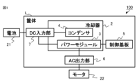
- FIG. 1 is a block diagram showing a configuration of a power conversion device according to a first embodiment
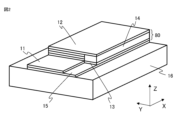
- 2 is a schematic perspective view showing a configuration of a main circuit connection portion of the power conversion device according to the first embodiment.
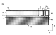
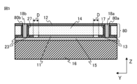
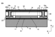
- FIG. 2 is a cross-sectional view showing a configuration of a main circuit connection portion of the power conversion device according to the first embodiment.
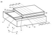
- FIG. 11 is a schematic perspective view showing the configuration of a main circuit connection portion of a power conversion device according to a second embodiment.
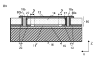
- FIG. 11 is a cross-sectional view showing the configuration of a main circuit connection portion of a power conversion device according to a second embodiment.
- FIG. 11 is a cross-sectional view showing the configuration of a main circuit connection portion of a power conversion device according to a third embodiment.
- FIG. 7A and 7B are cross-sectional views showing the configuration of a main circuit connection portion of a power conversion device according to embodiment 4.
- 13 is a cross-sectional view showing another configuration of the main circuit connection portion of the power conversion device according to embodiment 5.
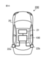
- FIG. FIG. 13 is a diagram showing the configuration of an electric vehicle using a power conversion device according to a sixth embodiment.
- Fig. 1 is a block diagram showing a configuration of a power conversion device 100 according to a first embodiment of the present invention.
- the power conversion device 100 is composed of a housing 1, a cooler 2, a power module 3, a capacitor 4, a control board 5, an AC output unit 6, and a DC input unit 7.
- the cooler 2 releases heat from heat-generating components, such as the power module, the capacitor, the AC output unit, and the DC input unit, to the outside of the power conversion device.
- FIG. 2 is a schematic perspective view showing the configuration of the main circuit connection section of the power conversion device 100 according to the first embodiment, and is a diagram showing the configuration of the main circuit connection section between the power module and the capacitor, between the power module and the AC output section, between the power module and the DC input section, and between the DC input section and the capacitor in the power conversion device 100 of FIG. 1.
- FIG. 3 is a cross-sectional view taken along the line AA in FIG. 2.
- the main circuit wiring section inserts high voltage wiring from the DC input section to the capacitor, from the capacitor to the power module, and from the DC input section to the power module section.
- the main circuit wiring portion in embodiment 1 is configured such that the circuit board 80 sandwiches the base material 14 between the first conductor 11 and the second conductor 12.
- the first conductor 11 and the second conductor 12 are both made of metal and are formed from a material with excellent electrical and thermal conductivity, such as copper or aluminum. In this embodiment, copper is used.
- the base material 14 is an insulating resin.
- the circuit board 80 has a multi-layer structure and, in addition to the copper pattern such as the first conductor 11, has electronic components not shown (components other than the main circuit wiring are not shown).
- the current flows in the X direction in the first conductor 11 and in the -X direction in the second conductor 12, so that the current flows in the opposite directions (the opposite is also possible).
- the third conductor 13 has the same potential phase (band) as the second conductor 12, and is arranged on the back surface, which is the first surface of the circuit board 80, which is a different layer from the second conductor 12, via the relay portion 18a and the base material 14 provided in the through hole 80a formed in the circuit board 80.
- the relay portion 18a is formed from a material with excellent thermal conductivity.
- the third conductor 13 is arranged on the same plane as the first conductor 11, and extends on the circuit board 80 while maintaining an insulation distance D from the first conductor 11. At least one through hole 80a is formed in the circuit board 80.
- An insulating heat transfer material 15 is placed between the cooling section 16 and the first conductor 11.
- the insulating heat transfer material 15 has an insulating function and a heat dissipation function between the first conductor 11 and the third conductor 13 and the cooling section 16.
- the insulating heat transfer material 15 is in contact with some or all of the first conductor 11 and the third conductor 13, and is configured to be able to dissipate heat to the cooling section 16 in areas where heat dissipation is required.
- the first conductor 11, the third conductor 13, and the fourth conductor 17 formed on the side wall of the through hole 80a are constructed as separate parts, and are electrically connected when the circuit board 80 is molded.
- the first conductor 11 and the second conductor 12 form parallel plates with a relatively thin base material 14 in between, so the distance between the electrodes can be made shorter than with a molded bus bar, which has the effect of reducing inductance.
- the first conductor 11 and the third conductor 13 are arranged on the same plane, they also form parallel plates at the side portions, and further reduction in inductance can be expected.
- the main circuit is only cooled on one side, and the side opposite the cooled side dissipates heat through the base material and the cooling conductor, so it is not actively cooled and the top surface remains at a high temperature.
- the main circuit on the top layer is also configured to dissipate heat to the cooling section with high conductivity through relay section 18a and fourth conductor 17.
- using metal for relay portion 18a makes it possible to move heat to cooling portion 16 more efficiently than when only the side of relay portion 80a is made of metal (fourth conductor 17). If it becomes possible to transfer heat from second conductor 12 on the front surface, which is the second surface of circuit board 80, to cooling portion 16, it becomes possible to narrow the width of first conductor 11 and second conductor 12, and as a result, it becomes possible to miniaturize the power conversion device.
- the power conversion device 100 includes a first conductor 11 provided on the rear surface of the circuit board 80, a second conductor 12 provided on the front surface of the circuit board 80, at least a portion of which faces the first conductor 11 via the circuit board 80, and through which a current flows in the opposite direction to that of the first conductor 11, a third conductor 13 provided on the rear surface of the circuit board 80 while maintaining an insulation distance D from the first conductor 11, and through which a current flows in the same direction as that of the second conductor 12, and at least
- the fourth conductor 17 is provided on the side wall of one or more through holes 80a and connects the second conductor 12 and the third conductor 13, a relay portion 18a filled in the through hole 80a with a thermally conductive material, and a cooling portion 16 provided on each surface of the first conductor 11 and the third conductor 13 via an insulating heat transfer material 15.
- the inductance can be reduced not only in the facing portion but also in the adjacent portion.
- Embodiment 2 In the second embodiment, a case will be described in which the configuration of the third conductor 13 in the first embodiment is also provided on the opposite side across the first conductor 11.
- FIG. 4 is a schematic perspective view showing the configuration of the main circuit connection part of the power conversion device according to the second embodiment.
- FIG. 5 is a cross-sectional view taken along the line AA in FIG. 4.
- the main circuit wiring portion in embodiment 2 includes a fifth conductor 23 of the same configuration as the third conductor 13 on the opposite side of the circuit board 80 to the first conductor 11 of the third conductor 13.
- the fifth conductor 23 has the same potential phase (band) as the second conductor 12, and is arranged on the back surface of the circuit board 80, which is a different layer from the second conductor 12, via the relay portion 18b and the substrate 14 provided in the through hole 80b formed in the circuit board 80.
- the fifth conductor 23 is arranged on the same plane as the first conductor 11, and extends on the circuit board 80 while maintaining an insulating distance D from the first conductor 11. At least one through hole 80b is formed in the circuit board 80.
- the first conductor 11, the third conductor 13, and the sixth conductor 27 formed on the side wall of the relay portion 80b are constructed as separate parts, and are electrically connected when the circuit board 80 is molded.
- the first conductor 11 and the second conductor 12 form parallel plates with a relatively thin base material 14 in between, so the distance between the electrodes can be made shorter than with a molded bus bar, which has the effect of reducing inductance.
- the first conductor 11 and the fifth conductor 23 are arranged on the same plane, so they also form parallel plates on the side portions, which is expected to further reduce inductance.
- the above configuration also makes it possible to further increase the cooling efficiency of the second conductor 12 on the surface of the circuit board 80, thereby enabling the power conversion device to be further miniaturized. Furthermore, since the third conductor 13 and the fifth conductor 23 are arranged to sandwich the first conductor 11 from the left and right, the number of parallel plate locations is increased compared to the configuration of embodiment 1, making it possible to further reduce inductance.
- the rest of the configuration of the power conversion device 100 according to embodiment 2 is the same as that of the power conversion device 100 according to embodiment 1, and corresponding parts are given the same reference numerals and their description is omitted.
- the configuration of the first embodiment is provided with a fifth conductor 23 on the back surface of the circuit board 80, in which the first conductor 11 is sandwiched between the third conductor 13 at the insulation distance D and a current flows in the same direction as the second conductor 12, a sixth conductor 27 formed on the circuit board 80 by sandwiching the first conductor 11 between the through hole 80a and the through hole 80a, which is provided on the side wall of the through hole 80b and connects the second conductor 12 and the fifth conductor 23, and a relay portion 18b filled in the through hole 80b with a thermally conductive material. Therefore, compared to the configuration of the first embodiment, the number of parallel plate locations is increased, making it possible to further reduce inductance. In addition, it is possible to further increase the cooling efficiency, making it possible to further miniaturize the power conversion device.
- Embodiment 3 In the third embodiment, a case will be described in which the third conductor 13, the fifth conductor 23, and the first conductor 11 are provided over a wider area than the second conductor 12 in the first embodiment.
- Fig. 6 is a cross-sectional view showing the configuration of the main circuit connection part of the power conversion device according to embodiment 3.
- the main circuit wiring part in embodiment 3 is formed in a wide area on the circuit board 80, beyond the area where the third conductor 13 and the fifth conductor 23 face the second conductor 12 via the circuit board 80.
- the third conductor 13 and the fifth conductor 23 spread over a wide area in the cooling section 16 via the insulating heat transfer material 15, improving cooling performance.
- the third conductor 13, the fifth conductor 23, and the first conductor 11 are formed in a wide area beyond the area facing the second conductor 12 via the circuit board 80, so in addition to the effects of the first and second embodiments, the cooling performance is improved because the cooling section is spread over a wide area via the insulating heat transfer material. As a result, it is possible to reduce the width of the second conductor, improving the degree of freedom in the mounting layout of electronic components on the surface of the circuit board.
- Embodiment 4 In the first to third embodiments, the phases on the front and back sides of the circuit board are fixed, but in the fourth embodiment, a case in which the phases are interchangeable will be described.
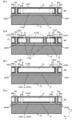
- FIGS. 7A to 7D are cross-sectional views showing the configuration of the main circuit connection part of the power conversion device according to embodiment 4.
- FIGS. 7A to 7D are cross-sectional views taken along the lines AA, BB, CC, and DD in FIG. 4, respectively.
- the potential of each conductor is indicated by (P) and (N).
- the main circuit wiring portion in embodiment 4 is configured such that the N phase (first conductor 11) on the back surface of the substrate 14 and the P phase (second conductor 12) on the front surface are switched from position AA to position DD in the circuit board 80, with the back surface of the substrate 14 being switched to the P phase (third conductor 13 or fifth conductor 23) and the front surface being switched to the N phase (seventh conductor 41).
- the seventh conductor 41 is placed on the opposite side of the substrate 14 to the first conductor 11 in a pattern with the same potential as the first conductor 11.
- the eighth conductor 42 and the ninth conductor 43 are placed on the opposite side of the substrate 14 to the seventh conductor 41 in a pattern with the same potential as the seventh conductor 41.
- the P phase (second conductor 12) is on the front surface of the circuit board 80, and the N phase (first conductor 11) is on the back surface, on the cooling section 16 side.
- the conductors on the front side and cooling side of the circuit board 80 are alternately arranged in the planar direction with the P phase and N phase maintaining an insulation distance D from position AA.
- the conductors are configured as P phase (second conductor 12 and fifth conductor 23)-N phase (seventh conductor 41 and first conductor 11)-P phase (second conductor 12 and third conductor 13). Note that in this fourth embodiment, only P phase-N phase-P phase is described, but it is also possible to narrow the width of the P phase and N phase, for example, and have multiple P phase and N phase configurations.
- the cross section shows that the N phase (seventh conductor 41) has moved to the surface side, and the P phase (second conductor 12, fifth conductor 23, and third conductor 13) is present on the surface and at the bottom.
- the N-phase (seventh conductor 41) spreads over the surface of the circuit board 80, and via relays 18a and 18b, the N-phase (eighth conductor 42 and ninth conductor 43) is also formed on the cooling section 16 side on the same plane as the P-phase (third conductor 13 or fifth conductor 23).
- the states shown in Figures 7A and 7D show a state in which the P phase and N phase are swapped. Note that in this fourth embodiment, a case in which the phases are swapped once has been described, but this is not limited to this. The arrangement of the P phase and N phase may be swapped multiple times on the circuit board 80. Also, although not shown in the figures in this fourth embodiment, depending on the cooling conditions, it is possible to reduce the areas of the eighth conductor 42, the ninth conductor 43, and the relay portions 18a and 18b, and reduce the number of relay points.
- the circuit board 80 is configured so that the potential phases of the conductors on the front and back sides are switched at least once, so that the conductors of both potential phases can be directly cooled by the cooler under the circuit board, and the temperature difference between the conductors is reduced. Therefore, the conductors can be cooled without excessively widening the width of the conductor layer to cool the high-temperature parts of the circuit board. This makes it possible to miniaturize the circuit board, and as a result, the power conversion device can also be miniaturized.
- Embodiment 5 In the fifth embodiment, a case in which a metal plate is mounted on the conductor surface of a circuit board 80 will be described.
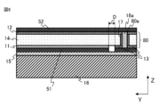
- Figure 8 is a cross-sectional view showing the configuration of the main circuit connection part of the power conversion device according to embodiment 5.
- the main circuit wiring part in embodiment 5 includes a first metal plate 51 on the surface of the first conductor 11, the third conductor 13, and the relay part 18a on the back surface of the circuit board 80, and a second metal plate 52 on the surface of the second conductor 12 and the relay part 18a on the front surface of the circuit board 80.
- the first metal plate 51 and the second metal plate 52 are mounted to each conductor by soldering. Note that, although the number of first metal plates 51 and second metal plates 52 is one each in the fifth embodiment, this is not limited to this. The number and mounting positions can be selected depending on the degree to which the current is to be dispersed.
- the third conductor 13 is provided on one side of the first conductor 11, but it may be provided on the opposite side of the first conductor 11.
- FIG. 9 is a cross-sectional view showing another configuration of the main circuit connection part of the power conversion device according to the fifth embodiment.
- the main circuit wiring part includes a fifth conductor 23 having the same configuration as the third conductor 13 on the opposite side of the circuit board 80 across the first conductor 11 from the third conductor 13, and a first metal plate 51 and a second metal plate 52 are mounted on each conductor as in the fifth embodiment.
- both the first metal plate 51 and the second metal plate 52 are provided, but it is also possible to provide only one of them.
- the power conversion device 100 includes a first metal plate 51 provided on the back surface of the circuit board 80 and/or a second metal plate 52 provided on the front surface. Therefore, the metal plate mounted on each conductor has the effect of increasing the cross-sectional area of the current path, which reduces the amount of heat generated by the conductor and makes it possible to reduce the temperature rise of each conductor. Furthermore, by increasing the thickness of the conductor to increase its cross-sectional area, it is possible to narrow the width of the conductor, which makes it possible to reduce the area of the circuit board and, as a result, to miniaturize the power conversion device.
- Embodiment 6 In the sixth embodiment, a case will be described in which the power conversion device 100 in the first embodiment is applied to an electric vehicle.
- FIG. 10 is a diagram showing the configuration of an electric vehicle 200 using a power conversion device 100 according to embodiment 6 of the present application.
- the electric vehicle 200 includes a power conversion device 100 according to any one of the first to fifth embodiments that converts DC power input from a battery 21 and outputs AC power, and a motor 22 (22a, 22b) that is driven by the AC power input from the power conversion device 100.
- the electric vehicle 200 using the power conversion device 100 according to the sixth embodiment includes the power conversion device 100 according to any one of the first to fifth embodiments that converts DC power input from the battery 21 and outputs AC power, and the motor 22 (22a, 22b) that is driven by the AC power input from the power conversion device 100. This reduces the inductance and size of the power conversion device, making it possible to reduce the size and weight of the electric vehicle.
Landscapes
- Engineering & Computer Science (AREA)
- Microelectronics & Electronic Packaging (AREA)
- Power Engineering (AREA)
- Inverter Devices (AREA)
Abstract
Description
図1は、本願の実施の形態1に係る電力変換装置100の構成を示すブロック図である。図1に示すように、電力変換装置100は、筐体1、冷却器2、パワーモジュール3、コンデンサ4、制御基板5、AC出力部6、DC入力部7で構成されている。冷却器2は、発熱部材、例えば、パワーモジュール、コンデンサ、AC出力部、DC入力部の熱を電力変換装置外へ放出する。
実施の形態2では、実施の形態1での第3の導体13の構成を第1の導体11を挟んだ反対側にも設けられている場合について説明する。
実施の形態3では、実施の形態1での第2の導体12に対して第3の導体13、第5の導体23、および第1の導体11の領域が広く設けられている場合について説明する。
実施の形態1から実施の形態3では回路基板上で表面側と裏面側の相が固定されていたが、実施の形態4では相が入れ替わる場合について説明する。
実施の形態5では、回路基板80の導体面に金属板を実装する場合について説明する。
実施の形態6では、実施の形態1での電力変換装置100を、電動車両へ適用した場合について説明する。
Claims (8)
- 基板の第1の面に設けられた第1の導体と、
前記基板の第2の面に設けられ、前記第1の導体と少なくとも一部が前記基板を介して対向し、前記第1の導体と反対方向に電流が流れる第2の導体と、
前記基板の第1の面に、前記第1の導体と絶縁距離を保って設けられ、前記第2の導体と同じ方向に電流が流れる第3の導体と、
前記基板に形成された少なくとも1以上の貫通孔の側壁に設けられ、前記第2の導体と前記第3の導体を接続する第4の導体と、
前記第1の導体および前記第3の導体の各表面に絶縁伝熱材を介して設けられた冷却部と、
を備えたことを特徴とする電力変換装置。 - 前記貫通孔の内部に、熱伝導性を有する部材で埋められた中継部を備えたことを特徴とする請求項1に記載の電力変換装置。
- 前記基板の第1の面に、前記第1の導体を前記第3の導体とで各絶縁距離を保って挟み、前記第2の導体と同じ方向に電流が流れる第5の導体と、
前記第1の導体を前記貫通孔とで挟んで前記基板に形成された、他方側の貫通孔の側壁に設けられ、前記第2の導体と前記第5の導体とを接続する第6の導体と、
を備えたことを特徴とする請求項1または請求項2に記載の電力変換装置。 - 前記他方側の貫通孔の内部に、熱伝導性を有する部材で埋められた中継部を備えたことを特徴とする請求項3に記載の電力変換装置。
- 前記第3の導体、前記第5の導体および前記第1の導体は、前記基板を介して前記第2の導体と対向している領域を超えて、広い領域に形成されていることを特徴とする請求項3または請求項4に記載の電力変換装置。
- 前記基板は、前記第1の導体と前記第2の導体の電位相の配置が少なくとも1回は入れ替わることを特徴とする請求項1から請求項5のいずれか1項に記載の電力変換装置。
- 前記基板の第1の面に設けられた第1の金属板と、前記基板の第2の面に設けられた第2の金属板と、を両方もしくはいずれか一方を備えたことを特徴とする請求項1から請求項6のいずれか1項に記載の電力変換装置。
- 電池から入力されたDC電力を変換してAC電力を出力する請求項1から請求項7のいずれか1項に記載の電力変換装置と、
前記電力変換装置から入力されたAC電力により駆動するモータと、
を備えたことを特徴とする電力変換装置を用いた電動車両。
Priority Applications (4)
| Application Number | Priority Date | Filing Date | Title |
|---|---|---|---|
| PCT/JP2023/020805 WO2024252462A1 (ja) | 2023-06-05 | 2023-06-05 | 電力変換装置及びそれを用いた電動車両 |
| DE112023006454.7T DE112023006454T5 (de) | 2023-06-05 | 2023-06-05 | Leistungskonvertierungsvorrichtung und elektrofahrzeug, das dieselbe verwendet |
| JP2025525438A JPWO2024252462A1 (ja) | 2023-06-05 | 2023-06-05 | |
| CN202380098782.4A CN121285937A (zh) | 2023-06-05 | 2023-06-05 | 功率转换装置及使用该功率转换装置的电动车辆 |
Applications Claiming Priority (1)
| Application Number | Priority Date | Filing Date | Title |
|---|---|---|---|
| PCT/JP2023/020805 WO2024252462A1 (ja) | 2023-06-05 | 2023-06-05 | 電力変換装置及びそれを用いた電動車両 |
Publications (1)
| Publication Number | Publication Date |
|---|---|
| WO2024252462A1 true WO2024252462A1 (ja) | 2024-12-12 |
Family
ID=93795220
Family Applications (1)
| Application Number | Title | Priority Date | Filing Date |
|---|---|---|---|
| PCT/JP2023/020805 Ceased WO2024252462A1 (ja) | 2023-06-05 | 2023-06-05 | 電力変換装置及びそれを用いた電動車両 |
Country Status (4)
| Country | Link |
|---|---|
| JP (1) | JPWO2024252462A1 (ja) |
| CN (1) | CN121285937A (ja) |
| DE (1) | DE112023006454T5 (ja) |
| WO (1) | WO2024252462A1 (ja) |
Citations (3)
| Publication number | Priority date | Publication date | Assignee | Title |
|---|---|---|---|---|
| JP2017188998A (ja) * | 2016-04-05 | 2017-10-12 | 三菱電機株式会社 | 電力変換装置 |
| JP2019187075A (ja) * | 2018-04-10 | 2019-10-24 | 三菱電機株式会社 | 電力変換装置 |
| JP2023040439A (ja) * | 2021-09-10 | 2023-03-23 | 三菱電機株式会社 | 電力変換装置 |
Family Cites Families (1)
| Publication number | Priority date | Publication date | Assignee | Title |
|---|---|---|---|---|
| JP6694589B2 (ja) | 2016-06-02 | 2020-05-20 | 株式会社ジェイテクト | パワーモジュール |
-
2023
- 2023-06-05 CN CN202380098782.4A patent/CN121285937A/zh active Pending
- 2023-06-05 WO PCT/JP2023/020805 patent/WO2024252462A1/ja not_active Ceased
- 2023-06-05 DE DE112023006454.7T patent/DE112023006454T5/de active Pending
- 2023-06-05 JP JP2025525438A patent/JPWO2024252462A1/ja active Pending
Patent Citations (3)
| Publication number | Priority date | Publication date | Assignee | Title |
|---|---|---|---|---|
| JP2017188998A (ja) * | 2016-04-05 | 2017-10-12 | 三菱電機株式会社 | 電力変換装置 |
| JP2019187075A (ja) * | 2018-04-10 | 2019-10-24 | 三菱電機株式会社 | 電力変換装置 |
| JP2023040439A (ja) * | 2021-09-10 | 2023-03-23 | 三菱電機株式会社 | 電力変換装置 |
Also Published As
| Publication number | Publication date |
|---|---|
| CN121285937A (zh) | 2026-01-06 |
| DE112023006454T5 (de) | 2026-03-19 |
| JPWO2024252462A1 (ja) | 2024-12-12 |
Similar Documents
| Publication | Publication Date | Title |
|---|---|---|
| US11153966B2 (en) | Electronic circuit device | |
| JP5289348B2 (ja) | 車載用電力変換装置 | |
| CN101622708B (zh) | 半导体模块及逆变器装置 | |
| US6765285B2 (en) | Power semiconductor device with high radiating efficiency | |
| JP4699820B2 (ja) | パワー半導体モジュール | |
| JP2006190972A (ja) | 電力用半導体装置 | |
| JP5469270B1 (ja) | 電子機器 | |
| US11652091B2 (en) | Solid state switching device including nested control electronics | |
| JP7760399B2 (ja) | 半導体装置 | |
| JP7628424B2 (ja) | 電子回路ユニット | |
| US12193143B2 (en) | Circuit board module | |
| JP2022526411A (ja) | 電子スイッチングユニット | |
| US20210368618A1 (en) | Circuit assembly and electrical junction box | |
| JP7570528B2 (ja) | 電力変換装置 | |
| CN121285937A (zh) | 功率转换装置及使用该功率转换装置的电动车辆 | |
| JP7640332B2 (ja) | 回路基板内に電気部品を内蔵する半導体装置 | |
| WO2022202248A1 (ja) | 電力変換装置 | |
| CN114975342A (zh) | 一种功率模块及车载功率电路 | |
| JP2024172899A (ja) | 電子装置 | |
| US20250300574A1 (en) | Power conversion device | |
| JP7531718B2 (ja) | 電子装置及び電動パワーステアリング装置 | |
| JP2025140615A (ja) | 立体構造基板 | |
| CN212992673U (zh) | 一种控制器、汽车电子水泵及汽车电子压缩机 | |
| WO2026069510A1 (ja) | 電力変換装置 | |
| CN118805450A (zh) | 电源模块的冷却结构 |
Legal Events
| Date | Code | Title | Description |
|---|---|---|---|
| 121 | Ep: the epo has been informed by wipo that ep was designated in this application |
Ref document number: 23940570 Country of ref document: EP Kind code of ref document: A1 |
|
| ENP | Entry into the national phase |
Ref document number: 2025525438 Country of ref document: JP Kind code of ref document: A |
|
| WWE | Wipo information: entry into national phase |
Ref document number: 2025525438 Country of ref document: JP |
|
| WWE | Wipo information: entry into national phase |
Ref document number: 112023006454 Country of ref document: DE |
|
| WWP | Wipo information: published in national office |
Ref document number: 112023006454 Country of ref document: DE |