WO2024247713A1 - 反射型マスクブランク、反射型マスク、反射型マスクブランクの製造方法、及び反射型マスクの製造方法 - Google Patents
反射型マスクブランク、反射型マスク、反射型マスクブランクの製造方法、及び反射型マスクの製造方法 Download PDFInfo
- Publication number
- WO2024247713A1 WO2024247713A1 PCT/JP2024/017857 JP2024017857W WO2024247713A1 WO 2024247713 A1 WO2024247713 A1 WO 2024247713A1 JP 2024017857 W JP2024017857 W JP 2024017857W WO 2024247713 A1 WO2024247713 A1 WO 2024247713A1
- Authority
- WO
- WIPO (PCT)
- Prior art keywords
- film
- reflective mask
- euv light
- absorbing
- multilayer reflective
- Prior art date
- Legal status (The legal status is an assumption and is not a legal conclusion. Google has not performed a legal analysis and makes no representation as to the accuracy of the status listed.)
- Ceased
Links
Images


Classifications
-
- G—PHYSICS
- G03—PHOTOGRAPHY; CINEMATOGRAPHY; ANALOGOUS TECHNIQUES USING WAVES OTHER THAN OPTICAL WAVES; ELECTROGRAPHY; HOLOGRAPHY
- G03F—PHOTOMECHANICAL PRODUCTION OF TEXTURED OR PATTERNED SURFACES, e.g. FOR PRINTING, FOR PROCESSING OF SEMICONDUCTOR DEVICES; MATERIALS THEREFOR; ORIGINALS THEREFOR; APPARATUS SPECIALLY ADAPTED THEREFOR
- G03F1/00—Originals for photomechanical production of textured or patterned surfaces, e.g., masks, photo-masks, reticles; Mask blanks or pellicles therefor; Containers specially adapted therefor; Preparation thereof
- G03F1/22—Masks or mask blanks for imaging by radiation of 100nm or shorter wavelength, e.g. X-ray masks, extreme ultraviolet [EUV] masks; Preparation thereof
- G03F1/24—Reflection masks; Preparation thereof
-
- G—PHYSICS
- G03—PHOTOGRAPHY; CINEMATOGRAPHY; ANALOGOUS TECHNIQUES USING WAVES OTHER THAN OPTICAL WAVES; ELECTROGRAPHY; HOLOGRAPHY
- G03F—PHOTOMECHANICAL PRODUCTION OF TEXTURED OR PATTERNED SURFACES, e.g. FOR PRINTING, FOR PROCESSING OF SEMICONDUCTOR DEVICES; MATERIALS THEREFOR; ORIGINALS THEREFOR; APPARATUS SPECIALLY ADAPTED THEREFOR
- G03F1/00—Originals for photomechanical production of textured or patterned surfaces, e.g., masks, photo-masks, reticles; Mask blanks or pellicles therefor; Containers specially adapted therefor; Preparation thereof
- G03F1/38—Masks having auxiliary features, e.g. special coatings or marks for alignment or testing; Preparation thereof
- G03F1/48—Protective coatings
-
- G—PHYSICS
- G03—PHOTOGRAPHY; CINEMATOGRAPHY; ANALOGOUS TECHNIQUES USING WAVES OTHER THAN OPTICAL WAVES; ELECTROGRAPHY; HOLOGRAPHY
- G03F—PHOTOMECHANICAL PRODUCTION OF TEXTURED OR PATTERNED SURFACES, e.g. FOR PRINTING, FOR PROCESSING OF SEMICONDUCTOR DEVICES; MATERIALS THEREFOR; ORIGINALS THEREFOR; APPARATUS SPECIALLY ADAPTED THEREFOR
- G03F1/00—Originals for photomechanical production of textured or patterned surfaces, e.g., masks, photo-masks, reticles; Mask blanks or pellicles therefor; Containers specially adapted therefor; Preparation thereof
- G03F1/54—Absorbers, e.g. of opaque materials
-
- G—PHYSICS
- G03—PHOTOGRAPHY; CINEMATOGRAPHY; ANALOGOUS TECHNIQUES USING WAVES OTHER THAN OPTICAL WAVES; ELECTROGRAPHY; HOLOGRAPHY
- G03F—PHOTOMECHANICAL PRODUCTION OF TEXTURED OR PATTERNED SURFACES, e.g. FOR PRINTING, FOR PROCESSING OF SEMICONDUCTOR DEVICES; MATERIALS THEREFOR; ORIGINALS THEREFOR; APPARATUS SPECIALLY ADAPTED THEREFOR
- G03F1/00—Originals for photomechanical production of textured or patterned surfaces, e.g., masks, photo-masks, reticles; Mask blanks or pellicles therefor; Containers specially adapted therefor; Preparation thereof
- G03F1/68—Preparation processes not covered by groups G03F1/20 - G03F1/50
- G03F1/80—Etching
Definitions
- the present disclosure relates to a reflective mask blank, a reflective mask, a method for manufacturing a reflective mask blank, and a method for manufacturing a reflective mask.
- EUV extreme ultraviolet
- EUV includes soft X-rays and vacuum ultraviolet light, and specifically refers to light with a wavelength of approximately 0.2 nm to 100 nm. At present, EUV with a wavelength of approximately 13.5 nm is mainly being considered.
- a reflective mask In EUVL, a reflective mask is used.
- a reflective mask has, in this order, a substrate such as a glass substrate, a multilayer reflective film that reflects EUV light, a protective film that protects the multilayer reflective film, and an absorbing film that absorbs EUV light.
- the absorbing film may not only absorb EUV light, but also shift the phase of the EUV light. In other words, the absorbing film may be a phase shift film.
- An opening pattern is formed in the absorbing film.
- the opening pattern in the absorbing film is transferred to a target substrate such as a semiconductor substrate. Transferring includes reducing and transferring.
- the reflective mask blank described in Patent Document 1 includes a substrate, a multilayer reflective film, a protective film, and an absorbing film in this order.
- MoCrRu film Mo: 20 at%, Cr: 46 at%, Ru: 34 at%), MoWRu film (Mo: 34 at%, W: 15 at%, Ru: 51 at%), MoAuRu film (Mo: 13 at%, Au: 12 at%, Ru: 75 at%), MoWRu film (Mo: 29 at%, W: 6 at%, Ru: 65 at%), MoWV film (Mo: 46 at%, W: 25 at%, V: 29 at%), etc. are disclosed.
- These absorbing films have a ratio (R A /R B ) of 0.05 to 0.25.
- R A is the reflectance of EUV light reflected by the multilayer reflective film and the protective film to the opposite side of the substrate via the absorbing film.
- R B is the reflectance of EUV light reflected by the multilayer reflective film and the protective film to the opposite side of the substrate without via the absorbing film.
- the reflective mask blank described in Patent Document 2 comprises a substrate, a multilayer reflective film, a protective film, and a phase shift film, in that order.
- the phase shift film includes a lower layer and a top layer.
- the lower layer of the phase shift film is a RuCrN film (Ru: 79.4 at%, Cr: 13.6 at%, N: 7.0 at%, refractive index: 0.900, extinction coefficient: 0.023)
- the top layer of the phase shift film is a RuCrO film (Ru: 18.1 at%, Cr: 29.5 at%, O: 52.4 at%, refractive index: 0.931, extinction coefficient: 0.027).
- the reflective mask blank described in Patent Document 3 comprises a substrate, a multilayer reflective film, a protective film, and a phase shift film, in that order.
- the phase shift film is a RuCr film (Ru: 7 at%, Cr: 93 at%, refractive index: 0.929, extinction coefficient: 0.037, relative reflectance: 6%).
- the phase shift film is a RuCr film (Ru: 39 at%, Cr: 61 at%, refractive index: 0.913, extinction coefficient: 0.030, relative reflectance: 15%).
- One aspect of the present disclosure provides an absorbing film whose main component is Cr, has good amorphous properties, and has a relative reflectance of less than 5%.
- a reflective mask blank has a substrate, a multilayer reflective film, a protective film, and an absorbing film, in this order.
- the multilayer reflective film reflects EUV light.
- the protective film protects the multilayer reflective film during processing of the absorbing film.
- the absorbing film absorbs EUV light.
- the absorbing film has a Cr-containing layer made of a CrN compound containing 50 at% or more of Cr and 10 at% or more of N.
- the Cr-containing layer has a full width at half maximum of the highest intensity peak in the 2 ⁇ range of 20° to 50° of 1.0° or more as measured by XRD using CuK ⁇ radiation, and the ratio of the reflectance of EUV light reflected by the multilayer reflective film and the protective film to the opposite side of the substrate via the absorbing film to the reflectance of EUV light reflected by the multilayer reflective film and the protective film to the opposite side of the substrate without the absorbing film is less than 5%.
- an absorbing film whose main component is Cr has good amorphous properties, and has a relative reflectance of less than 5%.
- FIG. 1 is a cross-sectional view showing a reflective mask blank according to one embodiment.
- FIG. 2 is a flowchart showing a method for manufacturing a reflective mask blank according to an embodiment.
- FIG. 3 is a cross-sectional view showing a reflective mask according to an embodiment.
- FIG. 4 is a flowchart showing a method for manufacturing a reflective mask according to an embodiment.
- FIG. 5(A) is a cross-sectional view showing an embodiment of preparation of a reflective mask blank
- FIG. 5(B) is a cross-sectional view showing an embodiment at the end of processing of a hard mask film
- FIG. 5(C) is a cross-sectional view showing an embodiment at the end of processing of an absorbing film.
- FIG. 6 is a cross-sectional view showing an example of EUV light reflected by the reflective mask of FIG.
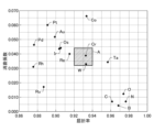
- FIG. 7 is a diagram showing an example of the refractive index and extinction coefficient of each element.
- the X-axis direction, the Y-axis direction, and the Z-axis direction are mutually orthogonal.
- the Z-axis direction is perpendicular to the first major surface 10a of the substrate 10.
- the X-axis direction is perpendicular to the incidence surface of the EUV light (the surface including the incident light beam and the reflected light beam). As shown in FIG. 6, the incident light beam is inclined toward the Y-axis positive direction as it moves toward the Z-axis negative direction, and the reflected light beam is inclined toward the Y-axis positive direction as it moves toward the Z-axis positive direction.
- the reflective mask blank 1 has, for example, a substrate 10, a multilayer reflective film 11, a protective film 12, an absorbing film 13, and a hard mask film 14, in this order.
- the multilayer reflective film 11, the protective film 12, the absorbing film 13, and the hard mask film 14 are formed on the first main surface 10a of the substrate 10, in this order.
- the multilayer reflective film 11 reflects EUV light.
- the protective film 12 protects the multilayer reflective film 11 from the first etching gas when the absorbing film 13 is processed.
- the absorbing film 13 absorbs EUV light.
- the absorbing film 13 may not only absorb EUV light, but also shift the phase of the EUV light. In other words, the absorbing film 13 may be a phase shift film.
- the hard mask film 14 protects a part of the absorbing film 13 from the first etching gas when the absorbing film 13 is processed.
- the reflective mask blank 1 may further have a functional film not shown in FIG. 1.
- the reflective mask blank 1 may have a conductive film on the opposite side of the multilayer reflective film 11 with respect to the substrate 10.
- the conductive film is formed on the second main surface 10b of the substrate 10.
- the second main surface 10b is the surface facing opposite to the first main surface 10a.
- the conductive film is used, for example, to attach the reflective mask 2 to an electrostatic chuck of an exposure device.
- the reflective mask blank 1 may have a diffusion barrier film (not shown) between the multilayer reflective film 11 and the protective film 12. The diffusion barrier film suppresses the diffusion of metal elements contained in the protective film 12 into the multilayer reflective film 11.
- the reflective mask blank 1 may have a buffer film between the protective film 12 and the absorbing film 13, although this is not shown.
- the buffer film protects the protective film 12 from the first etching gas that forms the opening pattern 13a in the absorbing film 13.
- the buffer film is etched more slowly than the absorbing film 13. Unlike the protective film 12, the buffer film will ultimately have the same opening pattern as the opening pattern 13a of the absorbing film 13.
- the method for manufacturing the reflective mask blank 1 includes, for example, steps S101 to S105 shown in FIG. 2.
- step S101 a substrate 10 is prepared.
- step S102 a multilayer reflective film 11 is formed on the first main surface 10a of the substrate 10.
- step S103 a protective film 12 is formed on the multilayer reflective film 11.
- step S104 an absorbing film 13 is formed on the protective film 12.
- step S105 a hard mask film 14 is formed on the absorbing film 13.
- the method for manufacturing the reflective mask blank 1 may further include a step of forming a functional film not shown in FIG. 2.
- the reflective mask 2 is produced, for example, using the reflective mask blank 1 shown in FIG. 1, and includes an opening pattern 13a in an absorbing film 13.
- the opening pattern 13a in the absorbing film 13 is transferred to a target substrate such as a semiconductor substrate. Transferring includes reducing and transferring. Note that the hard mask film 14 shown in FIG. 1 is not included in the reflective mask 2.
- a method for manufacturing a reflective mask 2 has steps S201 to S204 shown in Figure 4.
- a reflective mask blank 1 is prepared as shown in Figure 5 (A).
- the reflective mask blank 1 includes a resist film 16 as shown in Figure 5 (A).
- the resist film 16 is formed on a hard mask film 14.
- An opening pattern to be transferred to the absorbing film 13 is formed in the resist film 16.
- step S202 as shown in FIG. 5B, the hard mask film 14 is processed using a resist film 16 having an opening pattern.
- the hard mask film 14 is exposed to a second etching gas, which etches the hard mask film 14.
- the resist film 16 remains. As a result, the opening pattern of the resist film 16 is transferred to the hard mask film 14.
- the second etching gas is selected according to the combination of the material of the resist film 16 and the material of the hard mask film 14, and includes, but is not limited to, a fluorine-based gas.
- the fluorine -based gas includes at least one selected from, for example, CF4 gas, CHF3 gas , C2F6 gas , C3F6 gas , C4F6 gas, C4F8 gas, CH2F2 gas, CH3F gas , C3F8 gas, F2 gas, SF6 gas, and NF3 gas.
- the second etching gas may include an active gas or an inert gas in addition to the fluorine-based gas.
- the active gas includes, for example, O2 gas.
- the inert gas includes, for example, at least one selected from N2 gas, He gas, and Ar gas.
- the second etching gas is preferably a plasma gas.
- step S203 as shown in FIG. 5(C), the absorbing film 13 is processed using a hard mask film 14 having an opening pattern.
- the absorbing film 13 is exposed to a first etching gas, which etches the absorbing film 13.
- the hard mask film 14 has a higher resistance to the first etching gas than the absorbing film 13.
- the hard mask film 14 remains. As a result, the opening pattern of the hard mask film 14 is transferred to the absorbing film 13.
- the first etching gas is selected according to the combination of the material of the hard mask film 14 and the material of the absorbing film 13, and includes, but is not limited to, a chlorine-based gas and an oxygen-based gas.
- the chlorine-based gas includes at least one selected from, for example, Cl2 gas, SiCl4 gas, CHCl3 gas, CCl4 gas, and BCl3 gas.
- the oxygen-based gas includes at least one selected from, for example, O2 gas and O3 gas.
- the first etching gas may include an inert gas in addition to the chlorine-based gas and the oxygen-based gas.
- the inert gas includes at least one selected from, for example, N2 gas, He gas, and Ar gas.
- the first etching gas is preferably a plasma gas.
- step S204 although not shown, the hard mask film 14 is removed.
- a third etching gas is used to remove the hard mask film 14.
- the third etching gas contains, for example, a fluorine-based gas, similar to the second etching gas. It is preferable that the third etching gas is a plasma.
- a chemical solution may be used to remove the hard mask film 14.
- the substrate 10 the multilayer reflective film 11, the protective film 12, the absorbing film 13, and the hard mask film 14 will be described in this order.
- the substrate 10 is, for example, a glass substrate.
- the material of the substrate 10 is preferably quartz glass containing TiO 2. Quartz glass has a smaller linear expansion coefficient and a smaller dimensional change due to temperature change than general soda-lime glass. Quartz glass may contain 80% to 95% by mass of SiO 2 and 4% to 17% by mass of TiO 2. When the TiO 2 content is 4% to 17% by mass, the linear expansion coefficient is approximately zero near room temperature, and there is almost no dimensional change near room temperature. Quartz glass may contain a third component or impurity other than SiO 2 and TiO 2.
- the material of the substrate 10 may be crystallized glass in which a ⁇ -quartz solid solution is precipitated, silicon, metal, or the like.
- the substrate 10 has a first main surface 10a and a second main surface 10b facing opposite to the first main surface 10a.
- a multilayer reflective film 11 and the like are formed on the first main surface 10a.
- the size of the substrate 10 is, for example, 152 mm long and 152 mm wide.
- the vertical and horizontal dimensions may be 152 mm or more.
- the first main surface 10a and the second main surface 10b each have a square quality assurance area in the center.
- the size of the quality assurance area is, for example, 142 mm long and 142 mm wide.
- the vertical and horizontal dimensions may be 142 mm or more.
- the quality assurance area of the first main surface 10a preferably has a root-mean-square roughness (Rq) of 0.15 nm or less and a flatness of 100 nm or less. In addition, it is preferable that the quality assurance area of the first main surface 10a does not have any defects that cause phase defects.
- the multilayer reflective film 11 reflects EUV light.
- the multilayer reflective film 11 is, for example, a laminate of alternating high-refractive index layers and low-refractive index layers.
- the high-refractive index layers are made of, for example, silicon (Si)
- the low-refractive index layers are made of, for example, molybdenum (Mo), so a Mo/Si multilayer reflective film is used.
- Ru/Si multilayer reflective film, Mo/Be multilayer reflective film, Mo compound/Si compound multilayer reflective film, Si/Mo/Ru multilayer reflective film, Si/Mo/Ru/Mo multilayer reflective film, Si/Ru/Mo/Ru multilayer reflective film, Si/Ru/Mo multilayer reflective film, and Si/Ru/Mo multilayer reflective film can also be used as the multilayer reflective film 11.
- each layer constituting the multilayer reflective film 11 and the number of repeat units of the layers can be appropriately selected depending on the material of each layer and the reflectivity to EUV light.
- the multilayer reflective film 11 is a Mo/Si multilayer reflective film, in order to achieve a reflectivity of 60% or more for EUV light with an incident angle ⁇ (see FIG. 6) of 6°, Mo layers with a thickness of 2.3 ⁇ 0.1 nm and Si layers with a thickness of 4.5 ⁇ 0.1 nm can be stacked so that the number of repeat units is 30 or more and 60 or less. It is preferable that the multilayer reflective film 11 has a reflectivity of 60% or more for EUV light with an incident angle ⁇ of 6°. The reflectivity is more preferably 65% or more.
- the method for forming each layer constituting the multilayer reflective film 11 is, for example, a DC sputtering method, a magnetron sputtering method, an ion beam sputtering method, etc.
- a DC sputtering method a DC sputtering method
- a magnetron sputtering method a magnetron sputtering method
- an ion beam sputtering method etc.
- the protective film 12 is formed between the multilayer reflective film 11 and the absorbing film 13, and protects the multilayer reflective film 11.
- the protective film 12 protects the multilayer reflective film 11 from the first etching gas when the absorbing film 13 is processed, that is, in step S203.
- the protective film 12 is not removed even when exposed to the first etching gas, but remains on the multilayer reflective film 11.
- the protective film 12 contains at least one element selected from, for example, Ru, Rh, and Si. When the protective film 12 contains Rh, it may contain only Rh, but it may also contain an Rh compound.
- the Rh compound may contain, in addition to Rh, at least one element Z1 selected from Ru, Nb, Mo, Ta, Ir, Pd, Zr, Y, and Ti.
- the extinction coefficient can be reduced while suppressing an increase in the refractive index, and the absorption of EUV light by the protective film 12 (and thus a decrease in the reflectance of EUV light) can be suppressed. Furthermore, by adding Ta, Ir, Pd or Y to Rh, the resistance to the first etching gas can be improved.
- the Rh compound may contain, in addition to Rh, at least one element Z2 selected from N, O, C, and B.
- the element Z2 reduces the resistance of the protective film 12 to the first etching gas, but improves the smoothness of the protective film 12 by reducing the crystallinity of the protective film 12.
- the Rh compound containing the element Z2 has an amorphous structure or a microcrystalline structure. When the Rh compound has an amorphous structure or a microcrystalline structure, the X-ray diffraction profile of the Rh compound does not have a clear peak.
- the protective film 12 may be a film consisting of a single layer, or may be a multi-layer film having a lower layer and an upper layer.
- the lower layer and upper layer constituting the protective film 12 are formed in this order on the multilayer reflective film 11.
- the lower layer of the protective film 12 is a layer formed in contact with the uppermost surface of the multilayer reflective film 11.
- the upper layer of the protective film 12 is in contact with the lowermost surface of the absorbing film 13. In this way, by forming the protective film 12 into a multi-layer structure, materials with excellent predetermined functions can be used for each layer, making it possible to make the entire protective film 12 multifunctional.
- the upper layer of the protective film 12 preferably contains at least one element selected from Ru and Rh, more preferably contains Rh, and even more preferably contains an Rh compound.
- the lower layer of the protective film 12 preferably contains at least one element selected from Ru, Rh, Nb, Mo, Zr, Y, Si, C, N, and B, and more preferably contains Ru.
- the thickness of the protective film 12 below means the total film thickness of the multi-layer film. Note that a mixing layer formed by mixing the components contained in the multi-layer reflective film 11 and the components contained in the lower layer of the protective film 12 may be formed between the multi-layer reflective film 11 and the lower layer of the protective film 12.
- the thickness of the protective film 12 is preferably 1.0 nm to 4.0 nm, more preferably 2.0 nm to 3.5 nm, and even more preferably 2.5 nm to 3.0 nm. If the thickness of the protective film 12 is 1.0 nm or more, the etching resistance is good. Furthermore, if the thickness of the protective film 12 is 4.0 nm or less, the reflectance to EUV light is good.
- the density of the protective film 12 is preferably 10.0 g/cm 3 to 14.0 g/cm 3. If the density of the protective film 12 is 10.0 g/cm 3 or more, the etching resistance is good. Furthermore, if the density of the protective film 12 is 14.0 g/cm 3 or less, the decrease in reflectance for EUV light can be suppressed.
- the upper surface of the protective film 12, i.e., the surface of the protective film 12 on which the absorbing film 13 is formed, preferably has a root-mean-square roughness Rq of 0.20 nm or less, more preferably 0.17 nm or less. If the root-mean-square roughness Rq is 0.20 nm or less, the absorbing film 13 and the like can be formed smoothly on the protective film 12. In addition, scattering of EUV light can be suppressed, and the reflectance for EUV light can be improved.
- the root-mean-square roughness Rq is preferably 0.05 nm or more.
- the method for forming the protective film 12 is, for example, DC sputtering, magnetron sputtering, ion beam sputtering, etc.
- the Rh film is formed by DC sputtering
- an example of the film formation conditions is as follows. ⁇ Conditions for forming Rh film> Target: Rh target, Sputtering gas: Ar gas, Gas pressure: 1.0 ⁇ 10 ⁇ 2 Pa to 1.0 ⁇ 10 0 Pa, Target power density: 1.0 W/cm 2 to 8.5 W/cm 2 , Film formation rate: 0.020 nm/sec to 1.000 nm/sec, Film thickness: 1 nm to 10 nm.
- the absorbing film 13 absorbs EUV light.
- the absorbing film 13 is a film in which an opening pattern 13a is to be formed.
- the opening pattern 13a is not formed in the manufacturing process of the reflective mask blank 1, but is formed in the manufacturing process of the reflective mask 2.
- the absorbing film 13 may not only absorb EUV light, but may also shift the phase of the EUV light. In other words, the absorbing film 13 may be a phase shift film.
- the phase shift film shifts the phase of the second EUV light L2 relative to the first EUV light L1 shown in FIG. 6.
- the first EUV light L1 is light that passes through the opening pattern 13a without passing through the absorbing film 13, is reflected by the multilayer reflective film 11, and passes through the opening pattern 13a without passing through the absorbing film 13 again.
- the second EUV light L2 is light that passes through the absorbing film 13 while being absorbed by the absorbing film 13, is reflected by the multilayer reflective film 11, and passes through the absorbing film 13 while being absorbed by the absorbing film 13 again.
- the phase difference ( ⁇ 0) between the first EUV light L1 and the second EUV light L2 is, for example, 170° to 250°.
- the phase of the first EUV light L1 may be ahead of or behind the phase of the second EUV light L2.
- the absorbing film 13 uses the interference between the first EUV light L1 and the second EUV light L2 to improve the contrast of the transferred image.
- the transferred image is an image of the opening pattern 13a of the absorbing film 13 transferred onto the target substrate.
- the so-called projection effect occurs.
- the shadowing effect is caused by the fact that the incident angle ⁇ of the EUV light is not 0° (for example, 6°), and therefore an area where the sidewall blocks the EUV light occurs near the sidewall of the opening pattern 13a, causing a positional or dimensional shift in the transferred image.
- it is effective to lower the height of the sidewall of the opening pattern 13a, and thin the absorbing film 13.
- the thickness of the absorbing film 13 is, for example, 60 nm or less, and preferably 50 nm or less, in order to reduce the shadowing effect.
- the thickness of the absorbing film 13 is preferably 20 nm or more, and more preferably 30 nm or more, in order to ensure a phase difference between the first EUV light L1 and the second EUV light L2.
- the absorbing film 13 In order to reduce the thickness of the absorbing film 13 to reduce the shadowing effect while maintaining the phase difference between the first EUV light L1 and the second EUV light L2, it is effective to reduce the refractive index n of the absorbing film 13. Also, in order to reduce the reflectance for EUV light, it is effective to increase the extinction coefficient k of the absorbing film 13. Thus, the absorbing film 13 is required to have excellent optical properties.
- FIG. 7 is a diagram showing an example of the refractive index n and extinction coefficient k of each element.
- the refractive index n is the refractive index for EUV light (e.g., light with a wavelength of 13.5 nm).
- the extinction coefficient k is the extinction coefficient for EUV light (e.g., light with a wavelength of 13.5 nm).
- A is the range where the refractive index n is 0.920 to 0.940 and the extinction coefficient k is 0.032 to 0.044.
- a material having Cr as the main component is considered as a material having optical properties in range A.
- a CrN compound containing 50 at% or more of Cr and 10 at% or more of N is used as a material having optical properties in range A.
- optical properties of CrN compounds are taken from the database of the Center for X-Ray Optics, Lawrence Berkeley National Laboratory, or values calculated from the "incident angle dependence" of reflectance described below.
- the incidence angle ⁇ of the EUV light, the reflectance R for the EUV light, the refractive index n of the absorbing film 13, and the extinction coefficient k of the absorbing film 13 satisfy the following formula (1).
- R
- a number of combinations of the incident angle ⁇ and the reflectance R are measured, and the refractive index n and the extinction coefficient k are calculated by the least squares method so that the error between the multiple measurement data and equation (1) is minimized.
- the refractive index n of the CrN compound is preferably 0.920 to 0.940, and more preferably 0.920 to 0.930.
- the extinction coefficient k of the CrN compound is preferably 0.032 to 0.044, and more preferably 0.034 to 0.044.
- the relative reflectance Ra is the ratio (%) of the reflectance R2 of the second EUV light L2 to the reflectance R1 of the first EUV light L1.
- the first EUV light L1 is EUV light that is reflected by the multilayer reflective film 11 and the protective film 12 to the opposite side of the substrate 10 without passing through the absorbing film 13.
- the reflectance R1 of the first EUV light L1 is measured, for example, before the absorbing film 13 is formed.
- the reflectance R1 of the first EUV light L1 may be measured after the absorbing film 13 is formed and then removed.
- the second EUV light L2 is EUV light that is reflected by the multilayer reflective film 11 and the protective film 12 to the opposite side of the substrate 10 via the absorbing film 13.
- the reflectance R2 of the second EUV light L2 is measured, for example, after the absorbing film 13 is formed.
- the absorbing film 13 has a Cr-containing layer 13A made of a CrN compound. If the N content of the CrN compound is 10 at% or more, it has good amorphous properties and a relative reflectance Ra of less than 5%. If the relative reflectance Ra is less than 5%, the intensity difference between the first EUV light L1 and the second EUV light L2 can be improved, and the contrast of the transferred image can be improved.
- the N content of the CrN compound is preferably 10 at% or more, and more preferably 15 at% or more.
- the N content of the CrN compound is preferably 40 at% or less, more preferably 35 at% or less, and even more preferably 30 at% or less.
- Amorphousness is expressed by the diffraction line intensity in XRD using CuK ⁇ radiation.
- the full width at half maximum (FWHM) of the most intense peak in the 2 ⁇ range of 20° to 50° using XRD using CuK ⁇ radiation is 1.0° or more.
- the out-of-plane method is used for XRD.
- the full width at half maximum FWHM is 1.0° or more, the crystallinity of the Cr-containing layer 13A is low, and the roughness of the sidewall of the opening pattern 13a can be reduced.
- the full width at half maximum FWHM is preferably 2.0° or more, and more preferably 3.0° or more. The larger the full width at half maximum FWHM, the better, and it is preferable that there is no clear peak.
- the CrN compound contains 50 at% or more of Cr and 10 at% or more of N. It is preferable that the CrN compound further contains Ru.
- the Ru content of the CrN compound is preferably 5 at% or more, and more preferably 10 at% or more. If the Ru content of the CrN compound is 5 at% or more, the refractive index of the CrN compound is sufficiently small.
- the Ru content of the CrN compound is preferably 25 at% or less. If the Ru content of the CrN compound is 25 at% or less, the extinction coefficient k of the CrN compound will be 0.032 or more. The Ru content of the CrN compound is more preferably 20 at% or less.
- the ratio of the Ru content to the Cr content of the CrN compound (Ru/Cr) is preferably 0.60 or less. If the ratio of the Ru content to the Cr content of the CrN compound (Ru/Cr) is 0.60 or less, the extinction coefficient k of the CrN compound is 0.032 or more.
- the ratio of the Ru content to the Cr content of the CrN compound (Ru/Cr) is more preferably 0.50 or less, even more preferably 0.40 or less, even more preferably 0.30 or less, particularly preferably 0.25 or less, and most preferably 0.22 or less.
- the absorbing film 13 may have an oxide layer 13B made of an oxide on the opposite side of the protective film 12 from the Cr-containing layer 13A.
- the oxide layer 13B is formed, for example, when the surface of the Cr-containing layer 13A is naturally oxidized by the atmosphere. Note that the oxide layer 13B is not necessary, and the absorbing film 13 may be composed of only the Cr-containing layer 13A.
- the thickness of the oxide layer 13B is preferably 5 nm or less.
- the thickness of the oxide layer 13B is sufficiently thin that the physical properties (e.g., optical properties, etc.) of the absorbing film 13 are approximately equal to the physical properties of the Cr-containing layer 13A.
- the thickness of the oxide layer 13B is more preferably 4 nm or less.
- the thickness of the oxide layer 13B is preferably 0.1 nm or more.
- the method for forming the absorbing film 13 is, for example, a DC sputtering method, a magnetron sputtering method, an ion beam sputtering method, etc.
- the nitrogen content of the absorbing film 13 can be controlled by the content of N2 gas in the sputtering gas.
- the oxygen content of the absorbing film 13 can be controlled by the content of O2 gas in the sputtering gas.
- RuCrN film formation conditions ⁇ RuCrN film formation conditions> Target: Ru target and Cr target, Power density of Ru target: 1.0 W/cm 2 to 8.5 W/cm 2 , Power density of Cr target: 1.0 W/cm 2 to 8.5 W/cm 2 , Sputtering gas: a mixture of Ar gas and N2 gas, Volume ratio of N2 gas in the sputtering gas ( N2 /(Ar+ N2 )): 0.01 to 0.25, Film formation rate: 0.020 nm/sec to 0.060 nm/sec, Film thickness: 20 nm to 60 nm.
- the hard mask film 14 is formed on the opposite side of the protective film 12 with respect to the absorbing film 13, and is used to form an opening pattern 13a in the absorbing film 13.
- the hard mask film 14 enables the resist film 16 to be thinned.
- the hard mask film 14 preferably contains at least one element selected from Al, Hf, Y, Cr, Nb, Ti, Mo, Ta, and Si.
- the hard mask film 14 may further contain at least one element selected from O, N, C, and B.
- the thickness of the hard mask film 14 is preferably 2 nm or more and 30 nm or less, more preferably 2 nm or more and 25 nm or less, and even more preferably 2 nm or more and 10 nm or less.
- the hard mask film 14 can be formed, for example, by DC sputtering, magnetron sputtering, or ion beam sputtering.
- Examples 1 to 7 a reflective mask blank 1 was produced having a substrate 10, a multilayer reflective film 11, a protective film 12, and an absorbing film 13, in that order.
- a reflective mask blank 1 was produced with the same configuration except for the configuration of the absorbing film 13. Examples 1 to 3 are working examples, and Examples 4 to 7 are comparative examples.
- a SiO 2 -TiO 2 type glass substrate (6 inch (152 mm) square outer shape, 6.3 mm thick) was prepared.
- This glass substrate had a thermal expansion coefficient of 0.02 ⁇ 10 -7 /°C at 20°C, a Young's modulus of 67 GPa, a Poisson's ratio of 0.17, and a specific rigidity of 3.07 ⁇ 10 7 m 2 /s 2.
- the quality assurance area of the first main surface 10a of the substrate 10 was polished to have a root-mean-square roughness (Rq) of 0.15 nm or less and a flatness of 100 nm or less.
- a 100 nm thick Cr film was formed on the second main surface 10b of the substrate 10 by magnetron sputtering. The sheet resistance of the Cr film was 100 ⁇ / ⁇ .
- a Mo/Si multilayer reflective film was formed as the multilayer reflective film 11.
- the Mo/Si multilayer reflective film was formed by repeating the deposition of a Si layer (film thickness 4.5 nm) and a Mo layer (film thickness 2.3 nm) 40 times using an ion beam sputtering method.
- the total film thickness of the Mo/Si multilayer reflective film was 272 nm ((4.5 nm + 2.3 nm) x 40).
- Rh film (thickness 5 nm) was formed as the protective film 12.
- the Rh film was formed using the ion beam sputtering method.
- the Cr-containing layer shown in Table 1 was formed as the absorbing film 13.
- the Cr-containing layer was formed using a dual-target sputtering method.
- the chemical composition of the Cr-containing layer was measured using an X-ray photoelectron spectrometer (PHI 5000 VersaProbe) manufactured by ULVAC-PHI.
- the thicknesses of the Cr-containing layer and the oxide layer were measured by X-ray reflectivity.
- the surface of the Cr-containing layer was naturally oxidized in the atmosphere to form an oxide layer, and the thickness of the oxide layer was 5 nm or less.
- the experimental conditions and results for Examples 1 to 7 are shown in Table 1.
- the relative reflectance Ra was obtained by calculating the reflectances R1 and R2 using the optical simulation described in Experimental Approach to EUV Imaging Enhancement by Mask Absorber Height Optimization (2013) (authors: N. Davydova, R. Kruif, H. Rolff, B. Connolly, E. Setten, A. Lammers, D. Oorschot, N. Fukugami, Y. Kodera).
- the thickness of the oxide layer is sufficiently small that the relative reflectance Ra is approximately the same even with the oxide layer.
- the Cr-containing layer was composed of a CrN compound containing 50 at% or more of Cr and 10 at% or more of N.
- an absorbing film was obtained that had a refractive index of 0.920 to 0.940, an extinction coefficient of 0.032 to 0.044, good amorphousness, and a relative reflectance of less than 5%.
Landscapes
- Physics & Mathematics (AREA)
- General Physics & Mathematics (AREA)
- Preparing Plates And Mask In Photomechanical Process (AREA)
Priority Applications (3)
| Application Number | Priority Date | Filing Date | Title |
|---|---|---|---|
| JP2025523439A JPWO2024247713A1 (https=) | 2023-05-31 | 2024-05-14 | |
| KR1020257035848A KR20260015791A (ko) | 2023-05-31 | 2024-05-14 | 반사형 마스크 블랭크, 반사형 마스크, 반사형 마스크 블랭크의 제조 방법, 및 반사형 마스크의 제조 방법 |
| US19/356,372 US20260036898A1 (en) | 2023-05-31 | 2025-10-13 | Reflective mask blank, reflective mask, method of manufacturing reflective mask blank, and method of manufacturing reflective mask |
Applications Claiming Priority (2)
| Application Number | Priority Date | Filing Date | Title |
|---|---|---|---|
| JP2023-090180 | 2023-05-31 | ||
| JP2023090180 | 2023-05-31 |
Related Child Applications (1)
| Application Number | Title | Priority Date | Filing Date |
|---|---|---|---|
| US19/356,372 Continuation US20260036898A1 (en) | 2023-05-31 | 2025-10-13 | Reflective mask blank, reflective mask, method of manufacturing reflective mask blank, and method of manufacturing reflective mask |
Publications (1)
| Publication Number | Publication Date |
|---|---|
| WO2024247713A1 true WO2024247713A1 (ja) | 2024-12-05 |
Family
ID=93657755
Family Applications (1)
| Application Number | Title | Priority Date | Filing Date |
|---|---|---|---|
| PCT/JP2024/017857 Ceased WO2024247713A1 (ja) | 2023-05-31 | 2024-05-14 | 反射型マスクブランク、反射型マスク、反射型マスクブランクの製造方法、及び反射型マスクの製造方法 |
Country Status (5)
| Country | Link |
|---|---|
| US (1) | US20260036898A1 (https=) |
| JP (1) | JPWO2024247713A1 (https=) |
| KR (1) | KR20260015791A (https=) |
| TW (1) | TW202449495A (https=) |
| WO (1) | WO2024247713A1 (https=) |
Citations (9)
| Publication number | Priority date | Publication date | Assignee | Title |
|---|---|---|---|---|
| JP2010206156A (ja) * | 2009-02-04 | 2010-09-16 | Hoya Corp | 反射型マスクブランク及び反射型マスクの製造方法 |
| JP2015215602A (ja) * | 2014-04-22 | 2015-12-03 | 旭硝子株式会社 | Euvリソグラフィ用反射型マスクブランク、該マスクブランク用の機能膜付基板および、それらの製造方法 |
| WO2018159785A1 (ja) * | 2017-03-02 | 2018-09-07 | Hoya株式会社 | 反射型マスクブランク、反射型マスク及びその製造方法、並びに半導体装置の製造方法 |
| WO2020175354A1 (ja) * | 2019-02-28 | 2020-09-03 | Hoya株式会社 | 反射型マスクブランク、反射型マスク及びその製造方法、並びに半導体装置の製造方法 |
| US20210389662A1 (en) * | 2020-06-16 | 2021-12-16 | Samsung Electronics Co., Ltd. | Phase shift mask for extreme ultraviolet lithography and a method of manufacturing a semiconductor device using the same |
| US20210405519A1 (en) * | 2020-06-29 | 2021-12-30 | Taiwan Semiconductor Manufacturing Co., Ltd. | Euv photo masks and manufacturing method thereof |
| JP2022024617A (ja) * | 2020-07-28 | 2022-02-09 | Agc株式会社 | Euvリソグラフィ用反射型マスクブランク、euvリソグラフィ用反射型マスク、およびそれらの製造方法 |
| WO2022050156A1 (ja) * | 2020-09-04 | 2022-03-10 | Agc株式会社 | 反射型マスク、反射型マスクブランク、および反射型マスクの製造方法 |
| JP7272519B1 (ja) * | 2021-12-13 | 2023-05-12 | Agc株式会社 | 反射型マスクブランク、反射型マスク、反射型マスクブランクの製造方法、及び反射型マスクの製造方法 |
Family Cites Families (3)
| Publication number | Priority date | Publication date | Assignee | Title |
|---|---|---|---|---|
| KR102937232B1 (ko) | 2018-05-25 | 2026-03-10 | 호야 가부시키가이샤 | 반사형 마스크 블랭크, 반사형 마스크, 그리고, 반사형 마스크 및 반도체 장치의 제조 방법 |
| JP6929340B2 (ja) | 2019-11-21 | 2021-09-01 | Hoya株式会社 | 反射型マスクブランクおよび反射型マスク、並びに半導体装置の製造方法 |
| JP7616099B2 (ja) | 2021-03-03 | 2025-01-17 | 信越化学工業株式会社 | 反射型マスクブランク及びその製造方法 |
-
2024
- 2024-05-14 JP JP2025523439A patent/JPWO2024247713A1/ja active Pending
- 2024-05-14 WO PCT/JP2024/017857 patent/WO2024247713A1/ja not_active Ceased
- 2024-05-14 KR KR1020257035848A patent/KR20260015791A/ko active Pending
- 2024-05-15 TW TW113117914A patent/TW202449495A/zh unknown
-
2025
- 2025-10-13 US US19/356,372 patent/US20260036898A1/en active Pending
Patent Citations (9)
| Publication number | Priority date | Publication date | Assignee | Title |
|---|---|---|---|---|
| JP2010206156A (ja) * | 2009-02-04 | 2010-09-16 | Hoya Corp | 反射型マスクブランク及び反射型マスクの製造方法 |
| JP2015215602A (ja) * | 2014-04-22 | 2015-12-03 | 旭硝子株式会社 | Euvリソグラフィ用反射型マスクブランク、該マスクブランク用の機能膜付基板および、それらの製造方法 |
| WO2018159785A1 (ja) * | 2017-03-02 | 2018-09-07 | Hoya株式会社 | 反射型マスクブランク、反射型マスク及びその製造方法、並びに半導体装置の製造方法 |
| WO2020175354A1 (ja) * | 2019-02-28 | 2020-09-03 | Hoya株式会社 | 反射型マスクブランク、反射型マスク及びその製造方法、並びに半導体装置の製造方法 |
| US20210389662A1 (en) * | 2020-06-16 | 2021-12-16 | Samsung Electronics Co., Ltd. | Phase shift mask for extreme ultraviolet lithography and a method of manufacturing a semiconductor device using the same |
| US20210405519A1 (en) * | 2020-06-29 | 2021-12-30 | Taiwan Semiconductor Manufacturing Co., Ltd. | Euv photo masks and manufacturing method thereof |
| JP2022024617A (ja) * | 2020-07-28 | 2022-02-09 | Agc株式会社 | Euvリソグラフィ用反射型マスクブランク、euvリソグラフィ用反射型マスク、およびそれらの製造方法 |
| WO2022050156A1 (ja) * | 2020-09-04 | 2022-03-10 | Agc株式会社 | 反射型マスク、反射型マスクブランク、および反射型マスクの製造方法 |
| JP7272519B1 (ja) * | 2021-12-13 | 2023-05-12 | Agc株式会社 | 反射型マスクブランク、反射型マスク、反射型マスクブランクの製造方法、及び反射型マスクの製造方法 |
Also Published As
| Publication number | Publication date |
|---|---|
| JPWO2024247713A1 (https=) | 2024-12-05 |
| US20260036898A1 (en) | 2026-02-05 |
| TW202449495A (zh) | 2024-12-16 |
| KR20260015791A (ko) | 2026-02-03 |
Similar Documents
| Publication | Publication Date | Title |
|---|---|---|
| JP7513164B2 (ja) | 反射型マスクブランク、反射型マスク、反射型マスクブランクの製造方法、及び反射型マスクの製造方法 | |
| US20250155792A1 (en) | Reflective mask blank, reflective mask, method of manufacturing reflective mask blank, and method of manufacturing reflective mask | |
| JP7456562B1 (ja) | 反射型マスクブランク、及び反射型マスク | |
| WO2024162084A1 (ja) | 反射型マスクブランク、反射型マスク、反射型マスクブランクの製造方法、および反射型マスクの製造方法 | |
| WO2024247713A1 (ja) | 反射型マスクブランク、反射型マスク、反射型マスクブランクの製造方法、及び反射型マスクの製造方法 | |
| JP2025037417A (ja) | 反射型マスクブランク、反射型マスク、反射型マスクブランクの製造方法、及び反射型マスクの製造方法 | |
| WO2024225163A1 (ja) | 反射型マスクブランク、反射型マスクブランクの製造方法、及び反射型マスクの製造方法 | |
| JP2025116888A (ja) | 反射型マスクブランク、反射型マスク、反射型マスクブランクの製造方法、及び反射型マスクの製造方法 | |
| JP2024156304A (ja) | 反射型マスクブランク、反射型マスクブランクの製造方法、及び反射型マスクの製造方法 | |
| JP2025171653A (ja) | 反射型マスクブランク、反射型マスク、反射型マスクブランクの製造方法、及び反射型マスクの製造方法 | |
| JP2025157630A (ja) | 反射型マスクブランク、反射型マスク、反射型マスクブランクの製造方法、及び反射型マスクの製造方法 | |
| JP2026013650A (ja) | 反射型マスクブランク、反射型マスク、反射型マスクブランクの製造方法、及び反射型マスクの製造方法 | |
| JP2024135499A (ja) | 反射型マスクブランク、反射型マスク、反射型マスクブランクの製造方法、及び反射型マスクの製造方法 | |
| JP2026069718A (ja) | 反射型マスクブランクおよび反射型マスク | |
| WO2025120973A1 (ja) | 反射型マスクブランク、反射型マスク、反射型マスクブランクの製造方法、及び反射型マスクの製造方法 | |
| JP2024135147A (ja) | 反射型マスクブランク、反射型マスク、反射型マスクブランクの製造方法、及び反射型マスクの製造方法 | |
| WO2025079375A1 (ja) | 反射型マスクブランク、反射型マスク、反射型マスクブランクの製造方法、及び反射型マスクの製造方法 | |
| WO2025115566A1 (ja) | 反射型マスクブランク、反射型マスク、反射型マスクブランクの製造方法、及び反射型マスクの製造方法 | |
| WO2025225218A1 (ja) | 反射型マスクブランク、反射型マスクブランクの製造方法、及び反射型マスクの製造方法 | |
| JP2024134752A (ja) | 反射型マスクブランク、反射型マスク、反射型マスクブランクの製造方法、及び反射型マスクの製造方法 | |
| WO2025115587A1 (ja) | 反射型マスクブランク、反射型マスク、反射型マスクブランクの製造方法、及び反射型マスクの製造方法 |
Legal Events
| Date | Code | Title | Description |
|---|---|---|---|
| 121 | Ep: the epo has been informed by wipo that ep was designated in this application |
Ref document number: 24815197 Country of ref document: EP Kind code of ref document: A1 |
|
| ENP | Entry into the national phase |
Ref document number: 2025523439 Country of ref document: JP Kind code of ref document: A |
|
| NENP | Non-entry into the national phase |
Ref country code: DE |