WO2024247503A1 - 電源装置及び電源システム - Google Patents
電源装置及び電源システム Download PDFInfo
- Publication number
- WO2024247503A1 WO2024247503A1 PCT/JP2024/014540 JP2024014540W WO2024247503A1 WO 2024247503 A1 WO2024247503 A1 WO 2024247503A1 JP 2024014540 W JP2024014540 W JP 2024014540W WO 2024247503 A1 WO2024247503 A1 WO 2024247503A1
- Authority
- WO
- WIPO (PCT)
- Prior art keywords
- node
- power supply
- voltage
- supply device
- capacitor
- Prior art date
- Legal status (The legal status is an assumption and is not a legal conclusion. Google has not performed a legal analysis and makes no representation as to the accuracy of the status listed.)
- Ceased
Links
Images





Classifications
-
- H—ELECTRICITY
- H02—GENERATION; CONVERSION OR DISTRIBUTION OF ELECTRIC POWER
- H02M—APPARATUS FOR CONVERSION BETWEEN AC AND AC, BETWEEN AC AND DC, OR BETWEEN DC AND DC, AND FOR USE WITH MAINS OR SIMILAR POWER SUPPLY SYSTEMS; CONVERSION OF DC OR AC INPUT POWER INTO SURGE OUTPUT POWER; CONTROL OR REGULATION THEREOF
- H02M3/00—Conversion of DC power input into DC power output
- H02M3/02—Conversion of DC power input into DC power output without intermediate conversion into AC
- H02M3/04—Conversion of DC power input into DC power output without intermediate conversion into AC by static converters
- H02M3/10—Conversion of DC power input into DC power output without intermediate conversion into AC by static converters using discharge tubes with control electrode or semiconductor devices with control electrode
- H02M3/145—Conversion of DC power input into DC power output without intermediate conversion into AC by static converters using discharge tubes with control electrode or semiconductor devices with control electrode using devices of a triode or transistor type requiring continuous application of a control signal
- H02M3/155—Conversion of DC power input into DC power output without intermediate conversion into AC by static converters using discharge tubes with control electrode or semiconductor devices with control electrode using devices of a triode or transistor type requiring continuous application of a control signal using semiconductor devices only
Definitions
- This disclosure relates to a power supply device and a power supply system.
- a type of power supply device that uses switching elements is the multiphase converter.
- Multiphase converters can provide high output power and low output ripple.
- the present disclosure aims to provide a good power supply device and power supply system capable of performing multi-phase operation.
- the power supply device includes a first switching element provided between a reference node and a first node, a second switching element provided between the first node and a second node, a third switching element provided between the second node and a third node, a fourth switching element provided between the third node and a fourth node, a fifth switching element provided between the reference node and a fifth node, a sixth switching element provided between the fifth node and a sixth node, a seventh switching element provided between the sixth node and a seventh node, an eighth switching element provided between the seventh node and an eighth node, a first flying capacitor provided between the third node and the fifth node, and a second switching element provided between the seventh node and the first node.
- the inverter circuit includes a second flying capacitor between the first node and the output node, a first inductor between the first node and the output node, a second inductor between the fifth node and the output node, an output capacitor between the output node and the reference node, and a control circuit, and includes one or more intermediate capacitors between the second node and the sixth node and the reference node, or a single intermediate capacitor between the second node and the sixth node, and an input voltage higher than the voltage at the reference node is supplied to the fourth node and the eighth node, and the control circuit generates an output voltage at the output node lower than the input voltage by controlling the states of the first switching element to the eighth switching element.
- This disclosure makes it possible to provide a good power supply device and power supply system capable of performing multi-phase operation.
- FIG. 1 is a configuration diagram of a power supply device according to a reference embodiment.
- FIG. 2 is a diagram illustrating the operation of the power supply device of FIG.
- FIG. 3 is a configuration diagram of a power supply device according to a reference embodiment.
- FIG. 4 is a diagram illustrating the operation of the power supply device of FIG. 3 (state st1).
- FIG. 5 is a diagram illustrating the operation of the power supply device of FIG. 3 (state st2).
- FIG. 6 is a diagram illustrating the operation of the power supply device of FIG. 3 (state st3).
- FIG. 7 is a diagram illustrating the operation of the power supply device of FIG. 3 (state st4).
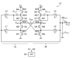
- FIG. 8 is a configuration diagram of the power supply device according to the first embodiment of the present disclosure.
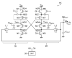
- FIG. 8 is a configuration diagram of the power supply device according to the first embodiment of the present disclosure.
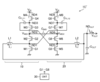
- FIG. 8 is a configuration diagram of the power supply device according to the first embodiment of the present disclosure.
- FIG. 9 is a diagram illustrating the operation of the power supply device according to the first embodiment of the present disclosure (mode MD1).
- FIG. 10 is a diagram illustrating the operation of the power supply device according to the first embodiment of the present disclosure (mode MD2).
- FIG. 11 is a diagram illustrating the operation of the power supply device according to the first embodiment of the present disclosure (mode MD3).
- FIG. 12 is a diagram illustrating the operation of the power supply device according to the first embodiment of the present disclosure (mode MD4).
- FIG. 13 is a diagram showing an internal configuration of a control circuit according to the first embodiment of the present disclosure.
- FIG. 14 is a timing chart of the power supply device according to the first embodiment of the present disclosure.
- FIG. 15 is a configuration diagram of a power supply device according to the second embodiment of the present disclosure.
- FIG. 16 is a configuration diagram of a power supply device according to a third embodiment of the present disclosure.
- FIG. 17 is a configuration diagram of a power supply device according to a fourth embodiment of the present disclosure.
- FIG. 18 is a configuration diagram of another power supply device according to the fourth embodiment of the present disclosure.
- FIG. 19 is a configuration diagram of still another power supply device according to the fourth embodiment of the present disclosure.
- FIG. 20 is a configuration diagram of a power supply system according to a fifth embodiment of the present disclosure.
- FIG. 21 is a relationship diagram of a plurality of clock signals in a power supply system according to the fifth embodiment of the present disclosure.
- FIG. 22 is an explanatory diagram of a method of configuring a multi-phase converter according to the fifth embodiment of the present disclosure.
- FIG. 23 is an explanatory diagram of a method of configuring a multi-phase converter according to the fifth embodiment of the present disclosure.
- FIG. 24 is an explanatory diagram of a method of configuring a multi-
- Ground refers to a reference conductive part having a reference potential of 0V (zero volts) or the reference potential of 0V itself.
- 0V zero volts
- ground When a certain component, electrode, or node is connected to ground, it means that the component, electrode, or node is connected to a reference node having a reference potential of 0V.
- the reference node and ground can be read as interchangeable terms.
- Level refers to the level of potential, and for any given signal or voltage, a high level has a higher potential than a low level.
- a high level signal or voltage strictly means that the signal or voltage level is at a high level
- a low level signal or voltage strictly means that the signal or voltage level is at a low level.
- the switch from low level to high level is called a rising edge
- the switch from high level to low level is called a falling edge.
- Any switching element can be composed of a transistor.
- a transistor configured as a FET (field effect transistor), including a MOSFET
- the on state refers to a state in which the drain and source of the transistor are conductive
- the off state refers to a state in which the drain and source of the transistor are non-conductive (cut-off state).
- MOSFET is understood to be an enhancement-type MOSFET.
- MOSFET is an abbreviation for "metal-oxide-semiconductor field-effect transistor.”
- the backgate of any MOSFET can be considered to be shorted to the source.
- the on and off states of any switching element may be simply expressed as on and off.
- switching from the off state to the on state will be expressed as turning on
- switching from the on state to the off state will be expressed as turning off.
- the period during which the switching element is in the on state will be referred to as the on period
- the period during which the switching element is in the off state will be referred to as the off period.
- the period during which the signal is at a high level is called a high-level period
- the period during which the signal is at a low level is called a low-level period.
- connections between multiple parts that form a circuit can be understood to refer to electrical connections.
- ⁇ Reference embodiment>> 1 shows a circuit diagram of a power supply device 910 according to a reference embodiment.
- the power supply device 910 includes four switching elements m1 to m4, capacitors Cfly and Cmid, an inductor La, and an output capacitor Cout.
- the power supply device 910 is a buck converter that generates an output voltage Vout by stepping down an input voltage Vin.
- the switching elements m1 to m4 are connected in series with each other. The switching elements are arranged in the order of m4, m3, m2, and m1 from the application terminal of the positive input voltage Vin toward the ground.
- a capacitor Cmid is provided between the connection node between the switching elements m2 and m3 and the ground.
- a capacitor Cfly is provided between the connection node between the switching elements m1 and m2 and the connection node between the switching elements m2 and m3.
- the capacitor Cmid functions as an intermediate capacitor, and the capacitor Cfly functions as a flying capacitor.
- An inductor La is provided between the connection node between the switching elements m1 and m2 and the output node NDout.
- the capacitor Cout functions as an output capacitor.
- the positive electrode of the capacitor Cout is connected to the output node NDout, and the negative electrode of the capacitor Cout is connected to the ground.
- the output voltage Vout is generated at the output node NDout.
- the control circuit (not shown) in the power supply device 910 switches the switching elements m1 to m4 based on the information on the output voltage Vout and the current information of the inductor La, as shown in FIG. 2, so that the set of switching elements m1 and m3 and the set of switching elements m2 and m4 are alternately turned on and off.
- This switching alternates between connecting the capacitors Cfly and Cmid in series or parallel.
- a switched capacitor circuit is formed by the switching elements m1 to m4 and the capacitors Cfly and Cmid, and as a result, in the steady state, the voltage Vmid of the positive electrode of the capacitor Cmid is approximately the voltage (Vin/2).
- the positive electrode of the capacitor Cmid is connected to the connection node between the switching elements m2 and m3. Meanwhile, a synchronous buck converter is formed by the switching elements m1 and m2, the inductor La, and the capacitor Cout. The synchronous buck converter generates the output voltage Vout by stepping down the voltage Vmid.
- Currents 921 and 922 are generated during the on-period of switching elements m2 and m4.
- Current 921 flows from the application terminal of the input voltage Vin through switching element m4 to capacitor Cfly, and contributes to charging capacitor Cfly.
- Current 922 flows from capacitor Cmid to output node NDout through switching element m2 and inductor La, and is generated by discharging capacitor Cmid.
- Currents 923 and 924 are generated during the on-period of switching elements m1 and m3.
- Current 923 flows from capacitor Cfly through switching element m3 to the positive electrode of capacitor Cmid.
- Current 923 is generated by discharging capacitor Cfly, and contributes to charging capacitor Cmid.
- Current 924 flows from ground to output node NDout through switching element m1 and inductor La.
- the power supply device 910 can be called a hybrid buck converter that combines a switched capacitor circuit and a synchronous buck converter. High efficiency can be achieved by using a switched capacitor circuit to reduce the input voltage Vin by half, and then further reducing the resulting voltage Vmid with a synchronous buck converter.
- a 12V output voltage Vout is generated from a 48V input voltage Vin.
- a square wave voltage (a square wave voltage that fluctuates between approximately 0V and 48V) is generated by switching the 48V input voltage Vin, and an output voltage of 12V is obtained by rectifying and smoothing the square wave voltage.
- a square wave voltage (a square wave voltage that fluctuates between approximately 0V and 24V) is generated by switching a voltage (Vin/2), and an output voltage of 12V is obtained by rectifying and smoothing the square wave voltage. Therefore, the power supply device 910 can keep switching losses low compared to the power supply device according to the reference method.
- the switching duty is relatively small.
- the impact of losses during periods when the instantaneous value of the square wave voltage rises and falls is relatively large.
- the input voltage to the synchronous buck converter is voltage (Vin/2), so the switching duty is relatively large compared to the reference method, leading to an improvement in switching loss.
- various parasitic capacitances are charged and discharged during the switching process, but in the power supply device 910, the input voltage to the synchronous buck converter is voltage (Vin/2), so the losses associated with charging and discharging the parasitic capacitances can be kept relatively low compared to the reference method.
- the power supply device 930 shown in FIG. 3 can be configured based on the power supply device 910.
- the power supply device 930 is a type of multi-phase converter.
- the power supply device 930 is configured by adding a switching element m5 and an inductor Lb to the power supply device 910 of FIG. 1.
- a first end of the capacitor Cfly is connected to the connection node between the switching elements m3 and m4, and a second end of the capacitor Cfly is connected to a first end of the switching element m5 and a first end of the inductor Lb.
- the second end of the switching element m5 is connected to ground.
- the second end of the inductor Lb is connected to the output node NDout together with the inductor La.
- An output voltage Vout is generated at the output node NDout.
- the power supply device 930 has a buck converter 931 and a stacked converter 932.
- the buck converter 931 has switching elements m1 and m2, an inductor La, and a capacitor Cout, and generates a desired output voltage by stepping down the voltage Vmid.
- the switching elements m1 and m2 function as a low-side switching element and a high-side switching element in the buck converter 931.
- the stacked converter 932 includes switching elements m3 to m5, a capacitor Cfly, and an inductor Lb, and generates a voltage Vmid from an input voltage Vin.
- the capacitor Cmid can be considered to be included in the components of the stacked converter 932.
- the stacked converter 932 also functions as a converter for one phase in a multiphase converter.
- the switching element m3 functions as a control switching element for charging the capacitor Cmid.
- the switching element m4 functions as a switching element for generating the voltage Vmid, and also functions as a high-side switching element for multiphase.
- the switching element m5 functions as a low-side switching element for multiphase.
- a control circuit (not shown) in the power supply device 930 controls the switching of switching elements m1 to m5 based on information about the output voltage Vout and current information about the inductor La. This switching control switches the states of the switching elements m1 to m5 between states st1 to st4 shown in Figures 4 to 7. In Figures 4 to 7, the current flow that occurs in each state is shown by multiple broken lines with arrows. It is assumed here that the power supply device 930 is operating in a continuous current mode.
- switching elements m2, m3, and m5 are in the ON state, and switching elements m1 and m4 are in the OFF state.
- currents 944 and 945 are generated along with the above-mentioned current 943.
- Current 944 corresponds to current 923 in FIG. 2.
- Current 944 flows from ground through switching element m5, capacitor Cfly, and switching element m3 toward the positive electrode of capacitor Cmid, and returns to ground through capacitor Cmid.
- Current 944 discharges capacitor Cfly while charging capacitor Cmid.
- Current 945 flows from ground through switching element m5 and inductor Lb to output node NDout.
- switching elements m1, m3, and m5 are in the on state, and switching elements m2 and m4 are in the off state.
- the above-mentioned currents 942, 944, and 945 are generated.
- state st1 the magnitudes of currents 941 and 942 are approximately the same.
- state st2 the magnitudes of currents 941 and 943 are approximately the same.
- switching elements m2 and m4 are on, so for capacitors Cfly and Cmid, state st2 is equivalent to a state in which capacitors Cfly and Cmid are connected in series.
- states st3 and st4 capacitors Cfly and Cmid are connected in parallel through switching elements m3 and m5.
- a switched capacitor circuit is formed in power supply device 930 by switching elements m1 to m5 and capacitors Cfly and Cmid. For this reason, in the steady state, the voltage Vmid of the positive electrode of capacitor Cmid is approximately the voltage (Vin/2).
- the output current (942, 943) from the buck converter 931 to the output node NDout, and the output current (941, 945) from the stacked converter 932 to the output node NDout are pulsating currents, and the former output current and the latter output current have different phases.
- the power supply device 930 is a multiphase converter (multiphase DC/DC converter) and has two phases.
- First Embodiment 8 shows the configuration of a power supply device 1A according to the first embodiment of the present disclosure.
- the power supply device 1A has a configuration similar to that of two power supply devices 930 shown in FIG.
- the power supply device 1A receives a positive input voltage V IN from a voltage source (not shown) and generates a positive output voltage V OUT by stepping down the input voltage V IN .
- the output voltage V OUT is lower than the input voltage V IN .
- the power supply device 1A stabilizes the output voltage V OUT at a predetermined target voltage. That is, in a steady state, the output voltage V OUT substantially coincides with the target voltage.
- the target voltage is referred to by the symbol "V TG ".
- intermediate voltages V MID1 and V MID2 are generated, and the output voltage V OUT is lower than the intermediate voltages V MID1 and V MID2 .
- the intermediate voltages V MID1 and V MID2 are substantially 1/2 of the input voltage V IN . Therefore, "V IN > 2 ⁇ V OUT " is established.
- the values of the input voltage V IN and the output voltage V OUT are arbitrary.
- the values of the input voltage V IN and the target voltage V TG are arbitrary.
- the input voltage V IN is 48 V
- the target voltage V TG i.e., the output voltage V OUT in the steady state
- the steady state refers to a state in which the output voltage VOUT rises from 0 V following startup of the power supply device 1A, reaches the target voltage VTG , and then the output voltage VOUT is stabilized at the target voltage VTG .
- the power supply device 1A includes converters 10 and 20, and a control circuit 30. As components of the converters 10 and 20, the power supply device 1A includes switching elements M1 to M8, capacitors C FLY1 , C FLY2 , C MID1 , C MID2 and C OUT , and inductors L1 to L4.
- the capacitors C FLY1 and C FLY2 may be referred to as flying capacitors.
- the capacitors C MID1 and C MID2 may be referred to as intermediate capacitors.
- the capacitor C OUT may be referred to as an output capacitor.
- the converter 10 is a first channel converter.
- the components of the converter 10 include switching elements M1 to M4, capacitors C FLY1 and C MID1 , and inductors L1 and L3.
- the converter 20 is a second channel converter.
- the components of the converter 20 include switching elements M5 to M8, capacitors C FLY2 and C MID2 , and inductors L2 and L4.
- the capacitor C OUT is shared by both the converters 10 and 20. That is, the capacitor C OUT is a component of each of the converters 10 and 20, and is shared by the converters 10 and 20.
- the converter 10 includes a first channel buck converter and a first channel stacked converter.
- the first channel buck converter includes switching elements M1 and M2 and an inductor L1, and operates in conjunction with a capacitor COUT to step down an intermediate voltage VMID1 to generate an output voltage VOUT at an output node NDOUT .
- the switching elements M1 and M2 function as a low-side switching element and a high-side switching element in the first channel buck converter.
- the first channel stacked converter includes switching elements M3 to M5, a capacitor C FLY1 , and an inductor L3, and generates an intermediate voltage V MID1 from an input voltage V IN .
- the capacitor C MID1 may be considered to be included in the components of the first channel stacked converter.
- the converter 10 itself is a two-phase multiphase converter.
- the first channel stacked converter also functions as a converter for one phase in the converter 10.
- the switching element M3 functions as a control switching element for charging the capacitor C MID1 .
- the switching element M4 functions as a switching element for generating the intermediate voltage V MID1 , and also functions as a high-side switching element for multiphase.
- the switching element M5 functions as a low-side switching element for multiphase.
- the converter 20 includes a second-channel buck converter and a second-channel stacked converter.
- the second-channel buck converter includes switching elements M5 and M6 and an inductor L2, and operates in conjunction with a capacitor COUT to step down an intermediate voltage VMID2 to generate an output voltage VOUT at an output node NDOUT .
- the switching elements M5 and M6 function as a low-side switching element and a high-side switching element in the second-channel buck converter.
- the second channel stacked converter includes switching elements M7, M8, and M1, a capacitor C FLY2 , and an inductor L4, and generates an intermediate voltage V MID2 from an input voltage V IN .
- the capacitor C MID2 may be considered to be included in the components of the second channel stacked converter.
- the converter 20 itself is a two-phase multiphase converter.
- the second channel stacked converter also functions as a converter for one phase in the converter 20.
- the switching element M7 functions as a control switching element for charging the capacitor C MID2 .
- the switching element M8 functions as a switching element for generating the intermediate voltage V MID2 , and also functions as a high-side switching element for multiphase.
- the switching element M1 functions as a low-side switching element for multiphase.
- the first channel buck converter, the first channel stacked converter, the second channel buck converter, and the second channel stacked converter each supply a current to the output node ND OUT , thereby generating an output voltage V OUT having a desired voltage value at the output node ND OUT .
- switching element M1 is used both as a low-side switching element in the buck converter of the first channel and as a low-side switching element for multi-phase in the stacked converter of the second channel.
- switching element M5 is used both as a low-side switching element in the buck converter of the second channel and as a low-side switching element for multi-phase in the stacked converter of the first channel.
- converters 10 and 20 are each two-phase multi-phase converters.
- power supply unit 1A converters 10 and 20 operate in parallel. If two power supply units 930 as shown in FIG. 3 were provided, a total of 10 switching elements would be required, whereas power supply unit 1A can achieve the same effect as two power supply units 930 operating in parallel with a total of eight switching elements, resulting in a reduction in the number of parts.
- the switching elements M1 to M8 are each configured with an N-channel MOSFET. For this reason, hereinafter, the switching elements M1 to M8 may be referred to as transistors M1 to M8.
- Transistors M1 to M4 are connected in series between ground and node ND4.
- Transistor M1 is provided between ground and node ND1
- transistor M2 is provided between nodes ND1 and ND2
- transistor M3 is provided between nodes ND2 and ND3
- transistor M4 is provided between nodes ND3 and ND4. More specifically, the source of transistor M1 is connected to ground.
- the drain of transistor M1 and the source of transistor M2 are connected to node ND1.
- the drain of transistor M2 and the source of transistor M3 are connected to node ND2.
- the drain of transistor M3 and the source of transistor M4 are connected to node ND3.
- the drain of transistor M4 is connected to node ND4.
- the signals supplied to the gates of transistors M1 to M4 are referred to as gate signals G1 to G4, respectively.
- Transistors M5 to M8 are connected in series between ground and node ND8.
- Transistor M5 is provided between ground and node ND5
- transistor M6 is provided between nodes ND5 and ND6
- transistor M7 is provided between nodes ND6 and ND7
- transistor M8 is provided between nodes ND7 and ND8.
- the source of transistor M5 is connected to ground.
- the drain of transistor M5 and the source of transistor M6 are connected to node ND5.
- the drain of transistor M6 and the source of transistor M7 are connected to node ND6.
- the drain of transistor M7 and the source of transistor M8 are connected to node ND7.
- the drain of transistor M8 is connected to node ND8.
- the signals supplied to the gates of transistors M5 to M8 are referred to as gate signals G5 to G8, respectively.
- the nodes ND4 and ND8 are power supply nodes that receive the input voltage VIN . That is, the input voltage VIN is supplied to the nodes ND4 and ND8.
- different reference symbols ND4, ND8 are assigned to the power supply node to which the drain of the transistor M4 is connected and the power supply node to which the drain of the transistor M8 is connected, but the nodes ND4 and ND8 may be a single node, or may be two separate nodes that receive the input voltage VIN .
- the capacitor C_MID1 is provided between the node ND2 and the ground. That is, a first end of the capacitor C_MID1 is connected to the node ND2, and a second end of the capacitor C_MID1 is connected to the ground. The first end of the capacitor C_MID1 corresponds to the positive electrode of the capacitor C_MID1 .
- the voltage at the node ND2 is the intermediate voltage V_MID1 . That is, a charge equivalent to the intermediate voltage V_MID1 is stored in the capacitor C_MID1 .
- the capacitor C_MID2 is provided between the node ND6 and the ground. That is, a first end of the capacitor C_MID2 is connected to the node ND6, and a second end of the capacitor C_MID2 is connected to the ground. The first end of the capacitor C_MID2 corresponds to the positive electrode of the capacitor C_MID2 .
- the voltage at the node ND6 is the intermediate voltage V_MID2 . That is, a charge equivalent to the intermediate voltage V_MID2 is stored in the capacitor C_MID2 .
- the inductor L1 is provided between the node ND1 and the output node ND OUT . That is, a first end of the inductor L1 is connected to the node ND1, and a second end of the inductor L1 is connected to the output node ND OUT .
- the capacitor C FLY1 is provided between the nodes ND3 and ND5. That is, a first end of the capacitor C FLY1 is connected to the node ND3, and a second end of the capacitor C FLY1 is connected to the node ND5.
- the inductor L3 is provided between the node ND5 and the output node ND OUT .
- a first end of the inductor L3 is connected to the node ND5 (and therefore connected to the second end of the capacitor C FLY1 ), and a second end of the inductor L3 is connected to the output node ND OUT .
- the inductor L2 is provided between the node ND5 and the output node ND OUT . That is, a first end of the inductor L2 is connected to the node ND5, and a second end of the inductor L2 is connected to the output node ND OUT .
- the capacitor C FLY2 is provided between the nodes ND7 and ND1. That is, a first end of the capacitor C FLY2 is connected to the node ND7, and a second end of the capacitor C FLY2 is connected to the node ND1.
- the inductor L4 is provided between the node ND1 and the output node ND OUT .
- a first end of the inductor L4 is connected to the node ND1 (and therefore to the second end of the capacitor C FLY2 ), and a second end of the inductor L4 is connected to the output node ND OUT .
- the capacitor COUT is provided between the output node NDOUT and the ground. That is, a first end of the capacitor COUT is connected to the output node NDOUT , and a second end of the capacitor COUT is connected to the ground. The first end of the capacitor COUT corresponds to the positive electrode of the capacitor COUT .
- the voltage at the output node NDOUT is the output voltage VOUT . That is, a charge equivalent to the output voltage VOUT is stored in the capacitor COUT .
- the control circuit 30 is connected to the gates of the transistors M1 to M8, and controls the states (on/off states) of the transistors M1 to M8 individually by supplying gate signals G1 to G8 to the transistors M1 to M8. By controlling the states of the transistors M1 to M8 with the control circuit 30, a desired output voltage V OUT lower than the input voltage V IN is generated at the output node ND OUT .
- the control circuit 30 may be formed of a semiconductor integrated circuit.
- any of the gate signals G1 to G8 is referred to as the gate signal Gx.
- the transistor Mx When the gate signal Gx has a high level, the transistor Mx is on, and when the gate signal Gx has a low level, the transistor Mx is off. Thus, during the high level period of the gate signal G1, the transistor M1 is on, and during the low level period of the gate signal G1, the transistor M1 is off. Similarly, during the high level period of the gate signal G2, the transistor M2 is on, and during the low level period of the gate signal G2, the transistor M2 is off. The same is true for the transistors M3 to M8.
- a high level gate signal Gx has a potential higher than the potential that is higher than the gate threshold voltage of the transistor Mx as viewed from the source potential of the transistor Mx.
- a low level gate signal Gx may have a potential equivalent to the source potential of the transistor Mx.
- the control circuit 30 sequentially switches the operating modes of the transistors M1 to M8 between modes MD1 to MD4. In other words, the control circuit 30 sequentially switches the states of the transistors M1 to M8 between the first to fourth states.
- Setting the operating modes of the transistors M1 to M8 to modes MD1, MD2, MD3, and MD4 corresponds to setting the states of the transistors M1 to M8 to the first, second, third, and fourth states, respectively. Modes MD1 to MD4 will be explained with reference to Figures 9 to 12.
- a current in a direction to increase the potential of the first end of capacitor C FLY1 (i.e., the potential of node ND3) based on the potential of the second end of capacitor C FLY1 (i.e., the potential of node ND5) is the charging current of capacitor C FLY1
- a current in the opposite direction is the discharging current of capacitor C FLY1 .
- a current in a direction to increase the potential of the first end of capacitor C FLY2 (i.e., the potential of node ND7) based on the potential of the second end of capacitor C FLY2 (i.e., the potential of node ND1) is the charging current of capacitor C FLY2
- a current in the opposite direction is the discharging current of capacitor C FLY2
- a current in a direction to increase intermediate voltage V MID1 is the charging current
- a current in a direction to decrease intermediate voltage V MID1 is the discharging current.
- a current that increases the intermediate voltage V MID2 is a charging current
- a current that decreases the intermediate voltage V MID2 is a discharging current.
- the power supply device 1A operates in the continuous current mode.
- a current always flows from the first end to the second end of each of the inductors L1 to L4, that is, a current always flows through the inductors L1 to L4 in a direction in which the capacitor C OUT is charged.
- the current flowing through the inductor L1 is referred to as the inductor current I L1 .
- the currents flowing through the inductors L2, L3, and L4 are referred to as the inductor currents I L2 , I L3 , and I L4 , respectively.
- the output node ND OUT is connected to a load not shown.
- the load is any load that is driven based on the output voltage V OUT .
- the current supplied to the load from the output node ND OUT is referred to as the load current I LD .
- the load current I LD corresponds to the output current of the power supply device 1A.
- FIG. 9 shows the on/off states of transistors M1 to M8 in mode MD1 and the current flow that occurs in mode MD1.
- control circuit 30 controls transistors M2, M3, M5, and M8 to the on state, while controlling transistors M1, M4, M6, and M7 to the off state.
- the state in mode MD1 corresponds to state st3 in FIG. 6 for converter 10, and corresponds to state st1 in FIG. 4 for converter 20.
- currents 811 to 813 are generated in the converter 10.
- the currents 811, 812, and 813 correspond to the currents 943, 944, and 945 in FIG. 6 for the converter 10.
- the current 811 flows from the capacitor C MID1 through the switching element M2 and the inductor L1 toward the output node ND OUT , and is generated by discharging the capacitor C MID1 .
- the current 812 flows from the ground through the switching element M5, the capacitor C FLY1 , and the switching element M3 toward the first end of the capacitor C MID1 , and returns to the ground through the capacitor C MID1 .
- the current 812 discharges the capacitor C FLY1 while charging the capacitor C MID1 .
- the current 813 flows from the ground through the switching element M5 and the inductor L3 toward the output node ND OUT .
- currents 814 and 815 are generated in converter 20.
- currents 814 and 815 correspond to currents 941 and 942 in FIG. 4.
- Current 814 flows from node ND8 through switching element M8, capacitor C FLY2 , and inductor L4 to output node ND OUT .
- Capacitor C FLY2 is charged by current 814.
- Current 815 flows from ground through switching element M5 and inductor L2 to output node ND OUT .
- no charging or discharging of capacitor C MID2 occurs, and the accumulated charge of capacitor C MID2 is kept unchanged.
- FIG. 10 shows the on/off states of transistors M1 to M8 in mode MD2 and the current flow that occurs in mode MD2.
- control circuit 30 controls transistors M2, M4, M6, and M8 to the on state, while controlling transistors M1, M3, M5, and M7 to the off state.
- the state in mode MD2 corresponds to state st2 in FIG. 5 for converter 10, and also corresponds to state st2 in FIG. 5 for converter 20.
- the converter 10 In mode MD2, the converter 10 generates a current 816 together with the current 811.
- the currents 811 and 816 correspond to the currents 943 and 941 in FIG. 5 for the converter 10.
- the current 811 is generated by discharging the capacitor C_MID1 .
- the current 816 flows from the node ND4 through the switching element M4, the capacitor C_FLY1 , and the inductor L3 to the output node ND_OUT .
- the capacitor C_FLY1 is charged by the current 816.
- a current 817 is generated in the converter 20 together with the current 814.
- the currents 814 and 817 correspond to the currents 941 and 943 in FIG. 5 for the converter 20.
- the capacitor C_FLY2 is charged by the current 814.
- the current 817 is a current flowing from the capacitor C_MID1 through the switching element M6 and the inductor L2 toward the output node ND_OUT , and is generated by discharging the capacitor C_MID2 .
- FIG. 11 shows the on/off states of transistors M1 to M8 in mode MD3 and the current flow that occurs in mode MD3.
- control circuit 30 controls transistors M1, M4, M6, and M7 to the on state, while controlling transistors M2, M3, M5, and M8 to the off state.
- the state in mode MD3 corresponds to state st1 in FIG. 4 for converter 10, and to state st3 in FIG. 6 for converter 20.
- current 818 is generated in converter 10 together with current 816.
- currents 816 and 818 correspond to currents 941 and 942 in FIG. 4.
- capacitor C_FLY1 is charged by current 816.
- Current 818 flows from ground to output node ND_OUT through switching element M1 and inductor L1.
- no charging or discharging of capacitor C_MID1 occurs, and the accumulated charge of capacitor C_MID1 is kept unchanged.
- currents 819 and 820 are generated in the converter 20 together with the current 817.
- the currents 817, 819, and 820 correspond to the currents 943, 944, and 945 in FIG. 6 for the converter 20.
- the current 817 is generated by discharging the capacitor C_MID2 .
- the current 819 flows from the ground through the switching element M1, the capacitor C_FLY2 , and the switching element M7 to the first end of the capacitor C_MID2 , and returns to the ground through the capacitor C_MID2 .
- the current 819 discharges the capacitor C_FLY2 , while charging the capacitor C_MID2 .
- the current 820 flows from the ground through the switching element M1 and the inductor L4 to the output node ND_OUT .
- FIG. 12 shows the on/off states of transistors M1 to M8 in mode MD4 and the current flow that occurs in mode MD4.
- control circuit 30 controls transistors M1, M3, M5, and M7 to the on state, while controlling transistors M2, M4, M6, and M8 to the off state.
- the state in mode MD4 corresponds to state st4 in FIG. 7 for converter 10, and also corresponds to state st4 in FIG. 7 for converter 20.
- the magnitudes of the currents 818 and 816 are approximately the same.
- the magnitudes of the currents 811 and 816 are approximately the same.
- the state of mode MD2 is equivalent to a state in which the capacitors C FLY1 and C MID1 are connected in series.
- the capacitors C FLY1 and C MID1 are connected in parallel through the transistors M3 and M5.
- a switched capacitor circuit is formed by the transistors M1 to M5 and the capacitors C FLY1 and C MID1 . Therefore, in a steady state, the voltage across the capacitor C MID1 (i.e., the intermediate voltage V MID1 ) coincides with the voltage (V IN /2) corresponding to the divided voltage of the input voltage V IN . Strictly speaking, however, the intermediate voltage V MID1 fluctuates somewhat around the voltage (V IN /2).
- the magnitudes of the currents 815 and 814 are approximately the same.
- the magnitudes of the currents 817 and 814 are approximately the same.
- the state of mode MD2 is equivalent to a state in which the capacitors C FLY2 and C MID2 are connected in series.
- the capacitors C FLY2 and C MID2 are connected in parallel through the transistors M7 and M1.
- a switched capacitor circuit is formed by the transistors M5 to M8 and M1 and the capacitors C FLY2 and C MID2 . Therefore, in a steady state, the voltage across the capacitor C MID2 (i.e., the intermediate voltage V MID2 ) coincides with the voltage (V IN /2) corresponding to the divided voltage of the input voltage V IN . Strictly speaking, however, the intermediate voltage V MID2 fluctuates somewhat around the voltage (V IN /2).
- FIG. 13 shows the internal configuration of the control circuit 30.
- FIG. 14 shows a timing chart related to the operation of the control circuit 30. From top to bottom, FIG. 14 shows the waveforms of signals CLK1, CMPOUT1, CLK2, CMPOUT2, and G1 to G8.
- the control circuit 30 includes an error amplifier 31, ramp circuits 32_1 and 32_2, current information acquisition circuits 33_1 and 33_2, adders 34_1 and 34_2, PWM comparators 35_1 and 35_2, and controllers 36_1 and 36_2.
- the power supply device 1A includes resistors R1 and R2. The first end of the resistor R1 is connected to the output node ND OUT , the second end of the resistor R1 is connected to the first end of the resistor R2, and the second end of the resistor R2 is connected to the ground. A feedback voltage V FB corresponding to the output voltage V OUT is generated at the connection node between the resistors R1 and R2.
- the feedback voltage V FB is a divided voltage of the output voltage V OUT , and is therefore proportional to the output voltage V OUT .
- the resistors R1 and R2 form a feedback voltage generation circuit that generates the feedback voltage V FB .
- the feedback voltage V FB is supplied to the control circuit 30.
- the feedback voltage generating circuit may be understood as being included in the components of the control circuit 30.
- the output voltage VOUT itself may be used as the feedback voltage VFB .
- the feedback voltage VFB is information on the output voltage VOUT (more specifically, information indicating the value of the output voltage VOUT ).
- the error amplifier 31 is a current output type transconductance amplifier.
- the error amplifier 31 has an inverting input terminal, a non-inverting input terminal, and an output terminal.
- a feedback voltage VFB is supplied to the inverting input terminal of the error amplifier 31.
- a predetermined reference voltage VREF is supplied to the non-inverting input terminal of the error amplifier 31.
- the reference voltage VREF is a DC voltage having a predetermined positive voltage value, and is generated by a reference voltage generating circuit (not shown) in the control circuit 30.
- the output terminal of the error amplifier 31 is connected to a wiring WR_ERR . Note that, when starting up the power supply device 1A, soft start control may be performed to gradually increase the value of the reference voltage VREF from 0V to a predetermined positive voltage value, but the existence of the soft start control will be ignored below.
- the error amplifier 31 generates an error voltage V ERR corresponding to the difference between the feedback voltage V FB and the reference voltage V REF on the wiring WR ERR by outputting a current signal corresponding to the difference between the feedback voltage V FB and the reference voltage V REF from its output terminal. Specifically, when the feedback voltage V FB is lower than the reference voltage V REF , the error amplifier 31 outputs a current from its output terminal to the wiring WR ERR so that the error voltage V ERR increases, and when the feedback voltage V FB is higher than the reference voltage V REF , the error amplifier 31 draws a current from the wiring WR ERR to its output terminal so that the error voltage V ERR decreases.
- a phase compensation circuit including a capacitor may be connected between the wiring WR ERR and ground.
- the ramp circuit 32_1 generates a ramp voltage V RAMP1 that monotonically increases at a predetermined rate from a predetermined initial voltage V INT during an on-period of the transistor M2.
- the initial voltage V INT is, for example, 0 V, but may be different from 0 V.
- the ramp voltage V RAMP1 is fixed at the initial voltage V INT .
- the current information acquisition circuit 33_1 acquires current information of the inductor L1, and generates a sense voltage VIL1 indicating the current information of the inductor L1.
- the current information of the inductor L1 is information indicating the value of the inductor current IL1 .
- the sense voltage VIL1 has a voltage value proportional to the value of the inductor current IL1 with a positive proportionality coefficient. Therefore, the sense voltage VIL1 increases as the inductor current IL1 increases, and the sense voltage VIL1 decreases as the inductor current IL1 decreases.
- VIL1 kIV x IL1 ", where kIV is a predetermined positive coefficient.
- the sense voltage VIL1 may be generated in any manner.
- the sense voltage VIL1 may be generated by directly detecting the inductor current IL1 with a current sensor.
- the current sensor here may be a shunt resistor (not shown) inserted in series between the inductor L1 and the node ND1.
- the sense voltage VIL1 may be generated by detecting the current (hence the inductor current IL1 ) flowing through the transistor M2 during the on-period of the transistor M2, or by detecting the current (hence the inductor current IL1 ) flowing through the transistor M1 during the on-period of the transistor M1 .
- the sense voltage VIL1 may be generated by detecting the voltage at any point where a voltage corresponding to the inductor current IL1 is generated.
- the PWM comparator 35_1 compares the error voltage V ERR and the slope voltage V SLP1 , and generates and outputs a signal CMPOUT1 indicating the comparison result.
- the error voltage V ERR is input to the inverting input terminal of the PWM comparator 35_1
- the slope voltage V SLP1 is input to the non-inverting input terminal of the PWM comparator 35_1.
- the PWM comparator 35_1 outputs a low-level signal CMPOUT1 when "V SLP1 ⁇ V ERR " is satisfied, and outputs a high-level signal CMPOUT1 when "V SLP1 >V ERR " is satisfied.
- a signal CMPOUT1 and a reference clock signal CLK1 are input to the controller 36_1.
- the reference clock signal CLK1 is generated by an internal clock generating circuit (not shown) provided in the control circuit 30.
- the reference clock signal CLK1 is a rectangular wave signal having a predetermined frequency f PWM , and alternates between high and low signal levels.
- the duty of the reference clock signal CLK1 is arbitrary.
- the reference clock signal CLK1 has a low level in principle, and has a high level for a very short time at intervals of the reciprocal of the frequency f PWM (see FIG. 14).
- the controller 36_1 When a predetermined level change occurs in the reference clock signal CLK1, the controller 36_1 turns off the transistors M1 and M7 by generating a falling edge in the gate signals G1 and G7 (i.e., by switching the levels of the gate signals G1 and G7 from high to low), and turns on the transistors M2 and M8 by generating a rising edge in the gate signals G2 and G8 (i.e., by switching the levels of the gate signals G2 and G8 from low to high).
- the predetermined level change (first predetermined level change) in the reference clock signal CLK1 here is a change from low to high in the reference clock signal CLK1, but it may also be a change from high to low in the reference clock signal CLK1.
- the slope voltage V SLP1 rises monotonically and transitions from a state where "V SLP1 ⁇ V ERR " is satisfied to a state where "V SLP1 >V ERR " is satisfied, causing a rising edge in the signal CMPOUT1.
- the controller 36_1 turns on the transistors M1 and M7 by causing a rising edge in the gate signals G1 and G7, and turns off the transistors M2 and M8 by causing a falling edge in the gate signals G2 and G8.
- the ramp voltage V RAMP1 drops to the sufficiently low initial voltage V INT , returning to a state where "V SLP1 ⁇ V ERR " is satisfied, and a falling edge occurs quickly in the signal CMPOUT1.
- the time from when the transistors M1 and M7 are turned off and the transistors M2 and M8 are turned on to when the transistors M1 and M7 are turned on and the transistors M2 and M8 are turned off is referred to as time t ON1 .
- the ramp circuit 32_2 generates a ramp voltage VRAMP2 that monotonically rises at a predetermined rate of change from a predetermined initial voltage VINT during the on-period of the transistor M6.
- the initial voltage VINT is, for example, 0V, but may be different from 0V.
- the ramp voltage VRAMP2 is fixed at the initial voltage VINT .
- the ramp circuit 32_2 has the same configuration as the ramp circuit 32_1. Therefore, the rate of change of the ramp voltage VRAMP2 during the on-period of the transistor M6 is equal to the rate of change of the ramp voltage VRAMP1 during the on-period of the transistor M2.
- the current information acquisition circuit 33_2 acquires current information of the inductor L2 and generates a sense voltage VIL2 indicating the current information of the inductor L2.
- the current information of the inductor L2 is information indicating the value of the inductor current IL2 .
- the sense voltage VIL2 has a voltage value proportional to the value of the inductor current IL2 with a positive proportionality coefficient. Therefore, the sense voltage VIL2 increases as the inductor current IL2 increases, and the sense voltage VIL2 decreases as the inductor current IL2 decreases.
- VIL2 kIV x IL2
- the sense voltage VIL2 may be generated in any manner.
- the sense voltage VIL2 may be generated by directly detecting the inductor current IL2 with a current sensor.
- the current sensor here may be a shunt resistor (not shown) inserted in series between the inductor L2 and the node ND5.
- the sense voltage VIL2 may be generated by detecting the current (hence the inductor current IL2 ) flowing through the transistor M6 during the on-period of the transistor M6, or the current (hence the inductor current IL2 ) flowing through the transistor M5 during the on-period of the transistor M5.
- the sense voltage VIL2 may be generated by detecting the voltage at any point where a voltage corresponding to the inductor current IL2 is generated.
- the PWM comparator 35_2 compares the error voltage V ERR and the slope voltage V SLP2 , and generates and outputs a signal CMPOUT2 indicating the comparison result.
- the error voltage V ERR is input to the inverting input terminal of the PWM comparator 35_2, and the slope voltage V SLP2 is input to the non-inverting input terminal of the PWM comparator 35_2.
- the PWM comparator 35_2 outputs a low-level signal CMPOUT2 when "V SLP2 ⁇ V ERR " is satisfied, and outputs a high-level signal CMPOUT2 when "V SLP2 >V ERR " is satisfied.
- a signal CMPOUT2 and a shift clock signal CLK2 are input to the controller 36_2.
- the shift clock signal CLK2 is a signal obtained by shifting the phase of the reference clock CLK1. Therefore, the reference clock signal CLK1 and the shift clock signal CLK2 have the same frequency f PWM and different phases.
- the shift clock signal CLK2 has a low level in principle and has a high level for a short time at an interval of the reciprocal of the frequency f PWM (see FIG. 14).
- the shift clock signal CLK2 may be generated in the control circuit 30 based on the reference clock CLK1.
- the shift clock signal CLK2 is assumed to be a signal whose phase is delayed by 180° from the reference clock signal CLK1.
- the phase difference between the clock signals CLK1 and CLK2 is 180°.
- Setting the delay amount to 180° is optimal for minimizing the ripple of the output voltage V OUT .
- the amount of delay in phase of the shift clock signal CLK2 with respect to the phase of the reference clock signal CLK1 may be other than 180° (for example, it may be 170° or 190°).
- the controller 36_2 When a predetermined level change occurs in the shift clock signal CLK2, the controller 36_2 generates a falling edge in the gate signals G3 and G5 to turn off the transistors M3 and M5, and generates a rising edge in the gate signals G4 and G6 to turn on the transistors M4 and M6.
- the predetermined level change (second predetermined level change) in the shift clock signal CLK2 here is a change from a low level to a high level in the shift clock signal CLK2, but it may also be a change from a high level to a low level in the shift clock signal CLK2.
- the controller 36_2 turns on the transistors M3 and M5 by generating a rising edge in the gate signals G3 and G5, and turns off the transistors M4 and M6 by generating a falling edge in the gate signals G4 and G6.
- the ramp voltage V RAMP2 drops to the sufficiently low initial voltage V INT , returning to a state where "V SLP2 ⁇ V ERR " is satisfied, and a falling edge occurs quickly in the signal CMPOUT2.
- the time from when the transistors M3 and M5 are turned off and the transistors M4 and M6 are turned on to when the transistors M3 and M5 are turned on and the transistors M4 and M6 are turned off is referred to as time t ON2 .
- the operation modes of the transistors M1 to M8 are sequentially switched between modes MD1 to MD4 by the above-mentioned switching control by the controllers 36_1 and 36_2. That is, in the timing chart of Fig. 14, starting from mode MD3, the operation modes of the transistors M1 to M8 are switched from mode MD3 to mode MD2 at the rising edge of the reference clock signal CLK1, then switched from mode MD2 to mode MD1 at the rising edge of the signal CMPOUT2, then switched from mode MD1 to mode MD4 at the rising edge of the signal CMPOUT1, and then returned from mode MD4 to mode MD3 at the rising edge of the shift clock signal CLK2. Thereafter, the same operation is repeated.
- the length between the timing of a transition from mode MD3 to mode MD2 and the timing of the next transition from mode MD3 to mode MD2 matches the reciprocal of the frequency f PWM of the reference clock signal CLK1.
- the above-mentioned time tON1 depends on the error voltage V ERR (and therefore on the information of the output voltage V OUT ) and on the sense voltage V IL1 (and therefore on the current information of the inductor L1 ). That is, the controller 36_1 controls the switching of the transistors M1, M2, M7, and M8 in synchronization with the reference clock signal CLK1 based on the information of the output voltage V OUT and the current information of the inductor L1.
- the controller 36_1 After turning off the transistors M1 and M7 and turning on the transistors M2 and M8 in response to a predetermined level change in the reference clock signal CLK1, the controller 36_1 turns on the transistors M1 and M7 and turns off the transistors M2 and M8 when the time tON1 according to the information of the output voltage V OUT and the current information of the inductor L1 has elapsed.
- the above-mentioned time t ON2 depends on the error voltage V ERR (and therefore on the information of the output voltage V OUT ) and on the sense voltage V IL2 (and therefore on the current information of the inductor L2). That is, the controller 36_2 controls the switching of the transistors M3 to M6 in synchronization with the shift clock signal CLK2 based on the information of the output voltage V OUT and the current information of the inductor L2.
- the controller 36_2 After turning off the transistors M3 and M5 and turning on the transistors M4 and M6 in response to a predetermined level change in the shift clock signal CLK2, the controller 36_2 turns on the transistors M3 and M5 and turns off the transistors M4 and M6 after the time t ON2 according to the information of the output voltage V OUT and the current information of the inductor L2 has elapsed.
- Converters 10 and 20 have the same configuration.
- the switching control of transistors M1, M2, M7, and M8 based on the current information of inductor L1 is equivalent to the switching control of transistors M3, M4, M5, and M6 based on the current information of inductor L2. Therefore, multiphase operation is achieved with the output current of converter 10 and the output current of converter 20 balanced.
- the output current of the converter 10 is the sum of the inductor currents I L1 and I L3
- the output current of the converter 20 is the sum of the inductor currents I L2 and I L4 .
- the average of the output current of the buck converter of the first channel (i.e., the inductor current I L1 ) and the average of the output current of the stacked converter of the first channel (i.e., the inductor current I L3 ) are substantially the same.
- the average of the output current of the buck converter of the second channel i.e., the inductor current I L2
- the average of the output current of the stacked converter of the second channel i.e., the inductor current I L4
- the average of the inductor currents I L1 to I L4 at each timing are different from each other, the average of the inductor current I L1 , the average of the inductor current I L2 , the average of the inductor current I L3 , and the average of the inductor current I L4 are substantially equal.
- the output current of the first channel buck converter i.e., inductor current I L1
- the output current of the second channel buck converter i.e., inductor current I L2
- the output current of the first channel stacked converter i.e., inductor current I L3
- the output current of the second channel stacked converter i.e., inductor current I L4
- the output current of the first channel buck converter (i.e., inductor current I L1 ) and the output current of the first channel stacked converter (i.e., inductor current I L3 ) have different phases
- the output current of the second channel buck converter (i.e., inductor current I L2 ) and the output current of the second channel stacked converter (i.e., inductor current I L4 ) have different phases.
- the circuit configuration in Fig. 13 is an example, and as long as the above-mentioned balance regarding currents is achieved, the configuration of the control circuit 30 can be modified in various ways. For example, a modification may be applied in which the adders 34_1 and 34_2 are deleted from the control circuit 30 in Fig. 13, and instead, current information of the inductors L1 and L2 is fed back to the error amplifier 31 side.
- V SLP1 V RAMP1
- V SLP2 V RAMP2
- a voltage (V ERR - V IL1 ) is input to the inverting input terminal of the PWM comparator 35_1
- a voltage (V ERR - V IL2 ) is input to the inverting input terminal of the PWM comparator 35_2.
- capacitors C MID1 and C MID2 are provided in the power supply device 1A according to the first embodiment.
- those capacitors may be integrated into a single capacitor.
- FIG. 15 is a configuration diagram of the power supply device 1B according to the second embodiment of the present disclosure. Based on the power supply device 1A of FIG. 8, one of the capacitors C MID1 and C MID2 is deleted, and then the nodes ND2 and ND6 are shorted to obtain the power supply device 1B. Except for the above deletion and shorting, the configuration and operation of the power supply device 1B are the same as those of the power supply device 1A. In FIG. 15, the capacitor C MID2 is deleted.
- the power supply device 1B has only the capacitor C MID1 , and the capacitor C MID1 is shared between the converters 10 and 20.
- the nodes ND2 and ND6 are connected to each other, so that the intermediate voltage V MID1 at the node ND2 and the intermediate voltage V MID2 at the node ND6 are always equal, including during a transient response.
- the number of parts in the power supply device 1B is reduced compared to the power supply device 1A. Also, the total capacitance of the intermediate capacitors in the power supply device 1B may be reduced compared to the power supply device 1A. For example, when the capacitors C MID1 and C MID2 in the power supply device 1A each have a capacitance value of 10 ⁇ F (microfarads), the power supply device 1B may be able to provide only a 10 ⁇ F capacitor C MID1 as the intermediate capacitor.
- the intermediate capacitor functions as the input capacitance of the buck converter of each channel, depending on the magnitude of the required load current I LD , it may be necessary to provide the capacitor C MID1 in the power supply device 1B with a capacitance value exceeding 10 ⁇ F.
- FIG. 16 is a configuration diagram of the power supply device 1C according to the third embodiment of the present disclosure. Based on the power supply device 1A of FIG. 8, the power supply device 1C is obtained by replacing the capacitors C MID1 and C MID2 with a single capacitor C MID . At this time, in the power supply device 1C, the first end of the capacitor C MID is connected to the node ND2, and the second end of the capacitor C MID is connected to the node ND6.
- the configuration and operation of the power supply device 1C are the same as those of the power supply device 1A.
- the capacitor C MID functions as a single intermediate capacitor.
- the intermediate voltage V MID1 at the node ND2 and the intermediate voltage V MID2 at the node ND6 pulsate during the period in which the switching control of the transistors M1 to M8 is performed, but the average voltage of the intermediate voltage V MID1 and the average voltage of the intermediate voltage V MID2 are half the input voltage V IN , respectively.
- the number of parts in the power supply device 1C is reduced compared to the power supply device 1A.
- the total capacitance of the intermediate capacitors in the power supply device 1C may be reduced compared to the power supply device 1A.
- the capacitors C MID1 and C MID2 in the power supply device 1A each have a capacitance value of 10 ⁇ F (microfarads)
- the power supply device 1C may only require a capacitor C MID of 10 ⁇ F as the intermediate capacitor.
- the intermediate capacitor functions as the input capacitance of the buck converter of each channel, depending on the magnitude of the required load current I LD , it may be necessary to give the capacitor C MID in the power supply device 1C a capacitance value exceeding 10 ⁇ F.
- FIG. 8 may be modified to a power supply device 1A' in FIG. 17 by deleting the inductors L3 and L4.
- the power supply device 1B in FIG. 15 may be modified to a power supply device 1B' in FIG. 18 by deleting the inductors L3 and L4.
- the power supply device 1C in FIG. 16 may be modified to a power supply device 1C' in FIG. 19 by deleting the inductors L3 and L4.
- FIGS. 17, 18, and 19 are configuration diagrams of power supply devices 1A', 1B', and 1C' according to the fourth embodiment.
- power supply device 1A' As viewed from power supply device 1A, the only difference is that no current is generated passing through inductors L3 and L4; in other respects, the configuration and operation of power supply device 1A' are the same as those of power supply device 1A.
- power supply device 1B' As viewed from power supply device 1B, the only difference is that no current is generated passing through inductors L3 and L4; in other respects, the configuration and operation of power supply device 1B' are the same as those of power supply device 1B.
- power supply device 1C' as viewed from power supply device 1C, the only difference is that no current is generated passing through inductors L3 and L4; in other respects, the configuration and operation of power supply device 1C' are the same as those of power supply device 1C.
- each of the power supply devices 1A', 1B', and 1C' is a two-phase multiphase converter (a multiphase DC/DC converter).
- FIG. 20 shows the configuration of a power supply system SYS according to the fifth embodiment.
- the power supply system SYS includes n power supply modules PM, where n is any integer equal to or greater than 2.
- Each power supply module PM includes a power supply device 1.
- Each power supply device 1 is any of the power supply devices described in the first to fourth embodiments, and therefore may be the above-mentioned power supply devices 1A, 1B, 1C, 1A', 1B', or 1C'.
- the n power supply modules PM are made up of power supply modules PM[1] to PM[n].
- the power supply device 1 provided in a power supply module PM[i] is denoted as power supply device 1[i], where i represents any integer.
- the power supply device 1[i] itself may be the power supply module PM[i], or the power supply device 1[i] may be configured with other additional circuits to form the power supply module PM[i]. Any operation of the power supply module PM[i] described below may be understood as an operation of the power supply device 1[i].
- Each power supply device 1 has an output node ND OUT .
- the total of n output nodes ND OUT in the power supply devices 1[1] to 1[n] may be n nodes independent of each other. In this case, an independent output voltage V OUT is generated in each of the power supply devices 1[1] to 1[n], and n types of output voltages V OUT can be generated by the power supply devices 1[1] to 1[n] as a whole.
- the power supply devices 1[1] to 1[n] may all be the same power supply device. That is, for example, the power supply devices 1[1] to 1[n] may all be power supply devices 1A, all may be power supply devices 1B, or all may be power supply devices 1C. Of the six types of power supply devices consisting of power supply devices 1A, 1B, 1C, 1A', 1B', or 1C', two or more types of power supply devices may be mixed in the power supply devices 1[1] to 1[n]. In the following, each of the power supply devices 1[1] to 1[n] is assumed to be either power supply devices 1A, 1B, or 1C. That is, each power supply device 1 is assumed to be a two-phase multiphase converter. In this case, the power supply devices 1[1] to 1[n] as a whole can form a (2 ⁇ n)-phase multiphase converter.
- each power supply device 1 operates in synchronization with a clock signal.
- the clock signal of the power supply device 1[i] is referred to by the symbol "CLK[i]". That is, the power supply device 1[i] operates in synchronization with the clock signal CLK[i].
- the clock signal CLK[i] is a square wave signal having a predetermined frequency f PWM , and has alternating high and low signal levels.
- the power supply device 1[i] uses the clock signal CLK[i] as the above-mentioned reference clock signal CLK1.
- the clock signals CLK[1] to CLK[n] have the same frequency f PWM and different phases.
- FIG. 21 shows the waveforms of the clock signals CLK[1] to CLK[4] when "n ⁇ 4".
- the clock signal CLK[i+1] is a signal obtained by shifting the phase of the clock signal CLK[i] in the phase delay direction.
- the clock signal CLK[2] is a signal obtained by delaying the phase of the clock signal CLK[1] by a predetermined amount ⁇
- the clock signal CLK[3] is a signal obtained by further delaying the phase of the clock signal CLK[2] by a predetermined amount ⁇
- the clock signal CLK[4] is a signal obtained by further delaying the phase of the clock signal CLK[3] by a predetermined amount ⁇ .
- the amount of delay in the phase of the clock signal CLK[n] from the perspective of the clock signal CLK[1] is less than 360°.
- the predetermined amount ⁇ is 10°.
- the predetermined amount ⁇ is determined so that a multi-phase converter with (2 ⁇ n) phases as a whole can be configured by the power supply devices 1[1] to 1[n]. That is, for any different integers i and j that satisfy "1 ⁇ i ⁇ n" and "1 ⁇ j ⁇ n", the predetermined amount ⁇ is determined so that the first and third converter output currents in the power supply device 1[i] and the first and third converter output currents in the power supply device 1[j] all have different phases, and so that the second and fourth converter output currents in the power supply device 1[i] and the second and fourth converter output currents in the power supply device 1[j] all have different phases.
- the first, second, third, and fourth converter output currents in the power supply device 1[i] are the output current of the first channel buck converter (i.e., inductor current I L1 ), the output current of the second channel buck converter (i.e., inductor current I L2 ), the output current of the first channel stacked converter (i.e., inductor current I L3 ), and the output current of the second channel stacked converter (i.e., inductor current I L4 ) in the power supply device 1[i].
- the first, second, third, and fourth converter output currents in the power supply device 1[j] are the output current of the first channel buck converter (i.e., inductor current I L1 ), the output current of the second channel buck converter (i.e., inductor current I L2 ), the output current of the first channel stacked converter (i.e., inductor current I L3 ), and the output current of the second channel stacked converter (i.e., inductor current I L4 ) in the power supply device 1[j].
- the following first, second or third configuration method can be used to configure a (2 x n) phase multi-phase converter.
- the power supply module PM[1] functions as a master module, and the clock signals CLK[2] to CLK[n] are determined by a clock chain method based on the clock signal CLK[1] generated by the power supply module PM[1]. That is, the power supply module PM[1] (e.g., the control circuit 30 in the power supply device 1[1]) according to the first configuration method uses the clock signal CLK[1] as its own reference clock signal CLK1, generates a signal with the phase of the clock signal CLK[1] delayed by a predetermined amount ⁇ as the clock signal CLK[2], and supplies the generated clock signal CLK[2] to the power supply module PM[2].
- the clock signal CLK[1] e.g., the control circuit 30 in the power supply device 1[1]
- the power supply module PM[2] (e.g., the control circuit 30 in the power supply device 1[2]) according to the first configuration method uses the clock signal CLK[2] as its own reference clock signal CLK1, and generates a signal in which the phase of the clock signal CLK[2] is delayed by a predetermined amount ⁇ as the clock signal CLK[3], and supplies the generated clock signal CLK[3] to the power supply module PM[3].
- the power supply module PM[i] (e.g., the control circuit 30 in the power supply device 1[i]) according to the first configuration method uses the clock signal CLK[i] as its own reference clock signal CLK1, generates a signal in which the phase of the clock signal CLK[i] is delayed by a predetermined amount ⁇ as the clock signal CLK[i+1], and supplies the generated clock signal CLK[i+1] to the power supply module PM[i+1].
- the power supply module PM[n] (e.g., the control circuit 30 in the power supply device 1[n]) according to the first configuration method uses the clock signal CLK[n] as its own reference clock signal CLK1.
- the power supply module PM[n] does not need to generate a signal in which the phase of the clock signal CLK[n] is delayed by a predetermined amount ⁇ .
- the power supply module PM[1] functions as a master module, and the power supply module PM[1] (for example, the control circuit 30 in the power supply device 1[1]) generates all of the clock signals CLK[1] to CLK[n].
- the power supply module PM[1] (for example, the control circuit 30 in the power supply device 1[1]) according to the second configuration method uses the clock signal CLK[1] as its own reference clock signal CLK1, and supplies the clock signals CLK[2] to CLK[n] to the power supply modules PM[2] to PM[n], respectively.
- the power supply module PM[i] according to the second configuration method uses the supplied clock signal CLK[i] as its own reference clock signal CLK1.
- the third configuration method will be described with reference to FIG. 24.
- a host device HST is provided in the power supply system SYS.
- the host device HST is configured with a microcomputer or the like.
- the host device HST according to the third configuration method generates clock signals CLK[1] to CLK[n] and supplies the clock signals CLK[1] to CLK[n] to the power supply modules PM[1] to PM[n] as external clock signals, respectively.
- the power supply module PM[i] according to the third configuration method uses the supplied clock signal CLK[i] as its own reference clock signal CLK1.
- the power supply device 1 or the power supply system SYS can be applied to any device or system that requires a stable DC voltage.
- the power supply device 1 or the power supply system SYS may be applied to a power supply system for a data center.
- the output voltage V OUT in the power supply device 1 or the power supply system SYS may be 48 V
- the power supply device 1 or the power supply system SYS supplies the output voltage V OUT to a 48 V power bus.
- reducing power consumption in data centers has become an important issue, and a transition from a 12 V power bus to a 48 V power bus is progressing.
- the power supply device 1 or the power supply system SYS may be applied to a primary power supply in a vehicle such as an automobile.
- the power supply device 1 or the power supply system SYS may directly receive an input voltage V IN from a battery mounted on the vehicle to generate an output voltage V OUT , and the output voltage V OUT may function as a driving voltage for any system (e.g., an autonomous driving system of level 3 or higher) mounted on the vehicle.
- the power supply device 1 or the power supply system SYS may be applied to a power supply for a charging system.
- the charging system may charge a battery of an electric vehicle.
- the power supply device 1 or the power supply system SYS may be applied to a power supply for a base station.
- transistors M1 to M8 may be formed of P-channel MOSFETs, or N-channel MOSFETs and P-channel MOSFETs may be mixed among transistors M1 to M8.
- any of the transistors described above may be any type of transistor, provided that no disadvantage arises.
- any of the transistors described above as MOSFETs may be replaced with junction FETs, IGBTs (Insulated Gate Bipolar Transistors), or bipolar transistors, provided that no disadvantage arises.
- Any of the transistors has a first electrode, a second electrode, and a control electrode.
- a FET one of the first and second electrodes is the drain, the other is the source, and the control electrode is the gate.
- IGBT In an IGBT, one of the first and second electrodes is the collector, the other is the emitter, and the control electrode is the gate.
- a bipolar transistor that does not belong to the IGBT one of the first and second electrodes is the collector, the other is the emitter, and the control electrode is the base.
- a power supply device includes a first switching element (M1) provided between a reference node and a first node, a second switching element (M2) provided between the first node and a second node, a third switching element (M3) provided between the second node and a third node, a fourth switching element (M4) provided between the third node and a fourth node, a fifth switching element (M5) provided between the reference node and a fifth node, a sixth switching element (M6) provided between the fifth node and a sixth node, a seventh switching element (M7) provided between the sixth node and a seventh node, an eighth switching element (M8) provided between the seventh node and an eighth node, a first flying capacitor (C FLY1 ) provided between the third node and the fifth node, and a second flying capacitor (C FLY2 ) provided between the seventh node and the first node.
- M1 first flying capacitor
- C FLY1 first flying capacitor
- C FLY2 first flying capacitor
- a first inductor (L1) provided between the first node and an output node
- a second inductor (L2) provided between the fifth node and the output node
- an output capacitor (C OUT ) provided between the output node and the reference node
- a control circuit (30) and one or more intermediate capacitors are provided between the second node and the sixth node and the reference node (see, for example, FIG. 8 or FIG. 15), or a single intermediate capacitor is provided between the second node and the sixth node (see, for example, FIG.
- an input voltage (V IN ) higher than the voltage at the reference node is supplied to the fourth node and the eighth node, and the control circuit generates an output voltage (V OUT ) lower than the input voltage at the output node by controlling the states of the first switching element to the eighth switching element (first configuration).
- the control circuit may be configured to sequentially switch the operation modes of the first to eighth switching elements between a first mode, a second mode, a third mode, and a fourth mode (MD1 to MD4), control the second, third, fifth, and eighth switching elements to an on state and control the first, fourth, sixth, and seventh switching elements to an off state in the first mode, control the second, fourth, sixth, and eighth switching elements to an on state and control the first, third, fifth, and seventh switching elements to an off state in the second mode, control the first, fourth, sixth, and seventh switching elements to an on state and control the first, third, fifth, and seventh switching elements to an off state in the third mode, control the first, fourth, sixth, and seventh switching elements to an on state and control the second, third, fifth, and eighth switching elements to an off state in the fourth mode (second configuration).
- control circuit may be configured (third configuration) to sequentially switch the operating modes of the first switching element to the eighth switching element between the first mode to the fourth mode based on the output voltage information (V FB ), the current information of the first inductor (V IL1 ), and the current information of the second inductor (V IL2 ).
- the control circuit may have a first controller (36_1) configured to control the switching of the first, second, seventh, and eighth switching elements in synchronization with a reference clock signal (CLK1) based on the output voltage information and the current information of the first inductor, and a second controller (36_1) configured to control the switching of the third, fourth, fifth, and sixth switching elements in synchronization with a shift clock signal (CLK2) based on the output voltage information and the current information of the second inductor, and the shift clock signal may be a signal obtained by shifting the phase of the reference clock signal (fourth configuration).
- CLK1 reference clock signal
- CLK2 shift clock signal
- the first controller may be configured to turn off the first and seventh switching elements and turn on the second and eighth switching elements in response to a predetermined level change in the reference clock signal, and then turn on the first and seventh switching elements and turn off the second and eighth switching elements after a time (t ON1 ) corresponding to the output voltage information and the current information of the first inductor has elapsed
- the second controller may be configured to turn off the third and fifth switching elements and turn on the fourth and sixth switching elements in response to a predetermined level change in the shift clock signal, and then turn on the third and fifth switching elements and turn off the fourth and sixth switching elements after a time (t ON2 ) corresponding to the output voltage information and the current information of the second inductor has elapsed (fifth configuration).
- the power supply device may further include a third inductor (L3) provided between the fifth node and the output node, and a fourth inductor (L4) provided between the first node and the output node (sixth configuration).
- L3 third inductor
- L4 fourth inductor
- the one or more intermediate capacitors may be a first intermediate capacitor (C MID1 ) provided between the second node and the reference node, and a second intermediate capacitor (C MID2 ) provided between the sixth node and the reference node (seventh configuration).
- a configuration may be used in which the one or more intermediate capacitors include a single intermediate capacitor (C MID1 ), the second node and the sixth node are connected to each other, and the single intermediate capacitor is provided between the second node and the sixth node and the reference node.
- C MID1 single intermediate capacitor
- any of the first to fifth configurations there may be a configuration (ninth configuration) in which the single intermediate capacitor (C MID ) is provided between the second node and the sixth node.
- the power supply system (FIG. 20; SYS) according to one aspect of the present disclosure is a configuration (tenth configuration) that includes multiple power supply devices according to any of the first to ninth configurations described above.
- each power supply device may be operated in synchronization with a clock signal, and the multiple clock signals (CLK[1] to CLK[n]) for the multiple power supply devices may have the same frequency but different phases (eleventh configuration).
- the output nodes of the multiple power supply devices may be connected to each other (twelfth configuration).
- a power supply device (FIG. 20; SYS) is a power supply system including a plurality of power supply devices according to the fourth or fifth configuration described above, and the plurality of reference clock signals (CLK[1] to CLK[n]) in the plurality of power supply devices may have the same frequency and different phases (thirteenth configuration).
- the output nodes of the multiple power supply devices may be connected to each other (fourteenth configuration).
Landscapes
- Engineering & Computer Science (AREA)
- Power Engineering (AREA)
- Dc-Dc Converters (AREA)
Priority Applications (1)
| Application Number | Priority Date | Filing Date | Title |
|---|---|---|---|
| JP2025523321A JPWO2024247503A1 (https=) | 2023-05-31 | 2024-04-10 |
Applications Claiming Priority (2)
| Application Number | Priority Date | Filing Date | Title |
|---|---|---|---|
| JP2023089912 | 2023-05-31 | ||
| JP2023-089912 | 2023-05-31 |
Publications (1)
| Publication Number | Publication Date |
|---|---|
| WO2024247503A1 true WO2024247503A1 (ja) | 2024-12-05 |
Family
ID=93657730
Family Applications (1)
| Application Number | Title | Priority Date | Filing Date |
|---|---|---|---|
| PCT/JP2024/014540 Ceased WO2024247503A1 (ja) | 2023-05-31 | 2024-04-10 | 電源装置及び電源システム |
Country Status (2)
| Country | Link |
|---|---|
| JP (1) | JPWO2024247503A1 (https=) |
| WO (1) | WO2024247503A1 (https=) |
Citations (4)
| Publication number | Priority date | Publication date | Assignee | Title |
|---|---|---|---|---|
| US20190028031A1 (en) * | 2017-07-18 | 2019-01-24 | Texas Instruments Incorporated | Three-level converter using an auxiliary switched capacitor circuit |
| US20190207505A1 (en) * | 2017-12-29 | 2019-07-04 | Texas Instruments Incorporated | Multilevel converter using node voltage track and control |
| JP2020156161A (ja) * | 2019-03-19 | 2020-09-24 | 株式会社明電舎 | Fc型3レベル電力変換装置 |
| JP2021164400A (ja) * | 2020-04-01 | 2021-10-11 | 現代自動車株式会社Hyundai Motor Company | 直流/直流コンバータ |
-
2024
- 2024-04-10 WO PCT/JP2024/014540 patent/WO2024247503A1/ja not_active Ceased
- 2024-04-10 JP JP2025523321A patent/JPWO2024247503A1/ja active Pending
Patent Citations (4)
| Publication number | Priority date | Publication date | Assignee | Title |
|---|---|---|---|---|
| US20190028031A1 (en) * | 2017-07-18 | 2019-01-24 | Texas Instruments Incorporated | Three-level converter using an auxiliary switched capacitor circuit |
| US20190207505A1 (en) * | 2017-12-29 | 2019-07-04 | Texas Instruments Incorporated | Multilevel converter using node voltage track and control |
| JP2020156161A (ja) * | 2019-03-19 | 2020-09-24 | 株式会社明電舎 | Fc型3レベル電力変換装置 |
| JP2021164400A (ja) * | 2020-04-01 | 2021-10-11 | 現代自動車株式会社Hyundai Motor Company | 直流/直流コンバータ |
Also Published As
| Publication number | Publication date |
|---|---|
| JPWO2024247503A1 (https=) | 2024-12-05 |
Similar Documents
| Publication | Publication Date | Title |
|---|---|---|
| US8836301B2 (en) | Power supply unit | |
| US11588404B2 (en) | Semiconductor device and step-down multi-phase DC/DC converter | |
| CN101364767A (zh) | 半导体电路和开关电源装置 | |
| CN211046763U (zh) | 电子转换器和降压型开关转换器 | |
| US12542496B2 (en) | Hybrid power converter and power conversion | |
| TWI387189B (zh) | 直流對直流轉換器及其方法 | |
| CN111756243B (zh) | 谐振开关电容器转换器 | |
| JP2018521622A (ja) | インダクタ電流に基づいてブーストスイッチングレギュレータを制御するための回路および方法 | |
| EP4254764A1 (en) | Switching power supply, and control circuit and control method thereof | |
| US12155303B2 (en) | Switching converter including controller circuit driving switches | |
| US20230412077A1 (en) | Switching power supply circuit and switching power supply device | |
| CN116488434A (zh) | 升降压转换器及其控制电路 | |
| WO2024247503A1 (ja) | 電源装置及び電源システム | |
| JP7698491B2 (ja) | スリーレベルコンバータ、そのコントローラ回路および制御方法、それを用いた電子機器 | |
| WO2024247502A1 (ja) | 電源装置 | |
| JP2024005754A (ja) | 直列キャパシタ降圧コンバータおよびそのコントローラ回路および制御方法 | |
| WO2025018033A1 (ja) | 電源装置 | |
| JP2023013702A (ja) | 昇降圧コンバータ、そのコントローラ回路、それを用いた電子機器 | |
| WO2025018034A1 (ja) | 電源装置 | |
| JP2025098357A (ja) | スイッチング電源装置 | |
| JP7701818B2 (ja) | スイッチングコンバータ、そのコントローラ回路、それを用いた電子機器 | |
| JP7812852B2 (ja) | アンプ回路、スイッチング電源用回路及びスイッチング電源装置 | |
| JP7658834B2 (ja) | スイッチドキャパシタコンバータ、そのコントローラ回路および制御方法、それを用いた電子機器 | |
| JP7747458B2 (ja) | 共振スイッチドキャパシタコンバータ、そのコントローラ回路、それを用いた電子機器 | |
| JP2025187604A (ja) | 電源制御装置及びスイッチング電源装置 |
Legal Events
| Date | Code | Title | Description |
|---|---|---|---|
| 121 | Ep: the epo has been informed by wipo that ep was designated in this application |
Ref document number: 24814990 Country of ref document: EP Kind code of ref document: A1 |
|
| ENP | Entry into the national phase |
Ref document number: 2025523321 Country of ref document: JP Kind code of ref document: A |
|
| NENP | Non-entry into the national phase |
Ref country code: DE |