WO2024247286A1 - ボンディングワイヤ - Google Patents
ボンディングワイヤ Download PDFInfo
- Publication number
- WO2024247286A1 WO2024247286A1 PCT/JP2023/023777 JP2023023777W WO2024247286A1 WO 2024247286 A1 WO2024247286 A1 WO 2024247286A1 JP 2023023777 W JP2023023777 W JP 2023023777W WO 2024247286 A1 WO2024247286 A1 WO 2024247286A1
- Authority
- WO
- WIPO (PCT)
- Prior art keywords
- wire
- coating layer
- less
- concentration
- mass
- Prior art date
- Legal status (The legal status is an assumption and is not a legal conclusion. Google has not performed a legal analysis and makes no representation as to the accuracy of the status listed.)
- Ceased
Links
Images
Classifications
-
- B—PERFORMING OPERATIONS; TRANSPORTING
- B23—MACHINE TOOLS; METAL-WORKING NOT OTHERWISE PROVIDED FOR
- B23K—SOLDERING OR UNSOLDERING; WELDING; CLADDING OR PLATING BY SOLDERING OR WELDING; CUTTING BY APPLYING HEAT LOCALLY, e.g. FLAME CUTTING; WORKING BY LASER BEAM
- B23K35/00—Rods, electrodes, materials, or media, for use in soldering, welding, or cutting
- B23K35/02—Rods, electrodes, materials, or media, for use in soldering, welding, or cutting characterised by mechanical features, e.g. shape
- B23K35/0255—Rods, electrodes, materials, or media, for use in soldering, welding, or cutting characterised by mechanical features, e.g. shape for use in welding
- B23K35/0261—Rods, electrodes or wires
-
- B—PERFORMING OPERATIONS; TRANSPORTING
- B23—MACHINE TOOLS; METAL-WORKING NOT OTHERWISE PROVIDED FOR
- B23K—SOLDERING OR UNSOLDERING; WELDING; CLADDING OR PLATING BY SOLDERING OR WELDING; CUTTING BY APPLYING HEAT LOCALLY, e.g. FLAME CUTTING; WORKING BY LASER BEAM
- B23K35/00—Rods, electrodes, materials, or media, for use in soldering, welding, or cutting
- B23K35/22—Rods, electrodes, materials, or media, for use in soldering, welding, or cutting characterised by the composition or nature of the material
- B23K35/24—Selection of soldering or welding materials proper
- B23K35/30—Selection of soldering or welding materials proper with the principal constituent melting at less than 1550°C
- B23K35/302—Cu as the principal constituent
-
- H—ELECTRICITY
- H10—SEMICONDUCTOR DEVICES; ELECTRIC SOLID-STATE DEVICES NOT OTHERWISE PROVIDED FOR
- H10W—GENERIC PACKAGES, INTERCONNECTIONS, CONNECTORS OR OTHER CONSTRUCTIONAL DETAILS OF DEVICES COVERED BY CLASS H10
- H10W72/00—Interconnections or connectors in packages
- H10W72/01—Manufacture or treatment
- H10W72/015—Manufacture or treatment of bond wires
- H10W72/01515—Forming coatings
-
- H—ELECTRICITY
- H10—SEMICONDUCTOR DEVICES; ELECTRIC SOLID-STATE DEVICES NOT OTHERWISE PROVIDED FOR
- H10W—GENERIC PACKAGES, INTERCONNECTIONS, CONNECTORS OR OTHER CONSTRUCTIONAL DETAILS OF DEVICES COVERED BY CLASS H10
- H10W72/00—Interconnections or connectors in packages
- H10W72/01—Manufacture or treatment
- H10W72/015—Manufacture or treatment of bond wires
- H10W72/01551—Changing the shapes of bond wires
-
- H—ELECTRICITY
- H10—SEMICONDUCTOR DEVICES; ELECTRIC SOLID-STATE DEVICES NOT OTHERWISE PROVIDED FOR
- H10W—GENERIC PACKAGES, INTERCONNECTIONS, CONNECTORS OR OTHER CONSTRUCTIONAL DETAILS OF DEVICES COVERED BY CLASS H10
- H10W72/00—Interconnections or connectors in packages
- H10W72/01—Manufacture or treatment
- H10W72/015—Manufacture or treatment of bond wires
- H10W72/01565—Thermally treating
-
- H—ELECTRICITY
- H10—SEMICONDUCTOR DEVICES; ELECTRIC SOLID-STATE DEVICES NOT OTHERWISE PROVIDED FOR
- H10W—GENERIC PACKAGES, INTERCONNECTIONS, CONNECTORS OR OTHER CONSTRUCTIONAL DETAILS OF DEVICES COVERED BY CLASS H10
- H10W72/00—Interconnections or connectors in packages
- H10W72/071—Connecting or disconnecting
-
- H—ELECTRICITY
- H10—SEMICONDUCTOR DEVICES; ELECTRIC SOLID-STATE DEVICES NOT OTHERWISE PROVIDED FOR
- H10W—GENERIC PACKAGES, INTERCONNECTIONS, CONNECTORS OR OTHER CONSTRUCTIONAL DETAILS OF DEVICES COVERED BY CLASS H10
- H10W72/00—Interconnections or connectors in packages
- H10W72/071—Connecting or disconnecting
- H10W72/075—Connecting or disconnecting of bond wires
-
- H—ELECTRICITY
- H10—SEMICONDUCTOR DEVICES; ELECTRIC SOLID-STATE DEVICES NOT OTHERWISE PROVIDED FOR
- H10W—GENERIC PACKAGES, INTERCONNECTIONS, CONNECTORS OR OTHER CONSTRUCTIONAL DETAILS OF DEVICES COVERED BY CLASS H10
- H10W72/00—Interconnections or connectors in packages
- H10W72/50—Bond wires
-
- B—PERFORMING OPERATIONS; TRANSPORTING
- B23—MACHINE TOOLS; METAL-WORKING NOT OTHERWISE PROVIDED FOR
- B23K—SOLDERING OR UNSOLDERING; WELDING; CLADDING OR PLATING BY SOLDERING OR WELDING; CUTTING BY APPLYING HEAT LOCALLY, e.g. FLAME CUTTING; WORKING BY LASER BEAM
- B23K20/00—Non-electric welding by applying impact or other pressure, with or without the application of heat, e.g. cladding or plating
- B23K20/002—Non-electric welding by applying impact or other pressure, with or without the application of heat, e.g. cladding or plating specially adapted for particular articles or work
- B23K20/004—Wire welding
-
- B—PERFORMING OPERATIONS; TRANSPORTING
- B23—MACHINE TOOLS; METAL-WORKING NOT OTHERWISE PROVIDED FOR
- B23K—SOLDERING OR UNSOLDERING; WELDING; CLADDING OR PLATING BY SOLDERING OR WELDING; CUTTING BY APPLYING HEAT LOCALLY, e.g. FLAME CUTTING; WORKING BY LASER BEAM
- B23K2101/00—Articles made by soldering, welding or cutting
- B23K2101/36—Electric or electronic devices
- B23K2101/40—Semiconductor devices
-
- H—ELECTRICITY
- H10—SEMICONDUCTOR DEVICES; ELECTRIC SOLID-STATE DEVICES NOT OTHERWISE PROVIDED FOR
- H10W—GENERIC PACKAGES, INTERCONNECTIONS, CONNECTORS OR OTHER CONSTRUCTIONAL DETAILS OF DEVICES COVERED BY CLASS H10
- H10W72/00—Interconnections or connectors in packages
- H10W72/01—Manufacture or treatment
- H10W72/015—Manufacture or treatment of bond wires
-
- H—ELECTRICITY
- H10—SEMICONDUCTOR DEVICES; ELECTRIC SOLID-STATE DEVICES NOT OTHERWISE PROVIDED FOR
- H10W—GENERIC PACKAGES, INTERCONNECTIONS, CONNECTORS OR OTHER CONSTRUCTIONAL DETAILS OF DEVICES COVERED BY CLASS H10
- H10W72/00—Interconnections or connectors in packages
- H10W72/071—Connecting or disconnecting
- H10W72/075—Connecting or disconnecting of bond wires
- H10W72/07511—Treating the bonding area before connecting, e.g. by applying flux or cleaning
-
- H—ELECTRICITY
- H10—SEMICONDUCTOR DEVICES; ELECTRIC SOLID-STATE DEVICES NOT OTHERWISE PROVIDED FOR
- H10W—GENERIC PACKAGES, INTERCONNECTIONS, CONNECTORS OR OTHER CONSTRUCTIONAL DETAILS OF DEVICES COVERED BY CLASS H10
- H10W72/00—Interconnections or connectors in packages
- H10W72/071—Connecting or disconnecting
- H10W72/075—Connecting or disconnecting of bond wires
- H10W72/07541—Controlling the environment, e.g. atmosphere composition or temperature
-
- H—ELECTRICITY
- H10—SEMICONDUCTOR DEVICES; ELECTRIC SOLID-STATE DEVICES NOT OTHERWISE PROVIDED FOR
- H10W—GENERIC PACKAGES, INTERCONNECTIONS, CONNECTORS OR OTHER CONSTRUCTIONAL DETAILS OF DEVICES COVERED BY CLASS H10
- H10W72/00—Interconnections or connectors in packages
- H10W72/50—Bond wires
- H10W72/521—Structures or relative sizes of bond wires
- H10W72/522—Multilayered bond wires, e.g. having a coating concentric around a core
-
- H—ELECTRICITY
- H10—SEMICONDUCTOR DEVICES; ELECTRIC SOLID-STATE DEVICES NOT OTHERWISE PROVIDED FOR
- H10W—GENERIC PACKAGES, INTERCONNECTIONS, CONNECTORS OR OTHER CONSTRUCTIONAL DETAILS OF DEVICES COVERED BY CLASS H10
- H10W72/00—Interconnections or connectors in packages
- H10W72/50—Bond wires
- H10W72/521—Structures or relative sizes of bond wires
- H10W72/522—Multilayered bond wires, e.g. having a coating concentric around a core
- H10W72/523—Multilayered bond wires, e.g. having a coating concentric around a core characterised by the structures of the outermost layers, e.g. multilayered coatings
-
- H—ELECTRICITY
- H10—SEMICONDUCTOR DEVICES; ELECTRIC SOLID-STATE DEVICES NOT OTHERWISE PROVIDED FOR
- H10W—GENERIC PACKAGES, INTERCONNECTIONS, CONNECTORS OR OTHER CONSTRUCTIONAL DETAILS OF DEVICES COVERED BY CLASS H10
- H10W72/00—Interconnections or connectors in packages
- H10W72/50—Bond wires
- H10W72/551—Materials of bond wires
- H10W72/552—Materials of bond wires comprising metals or metalloids, e.g. silver
-
- H—ELECTRICITY
- H10—SEMICONDUCTOR DEVICES; ELECTRIC SOLID-STATE DEVICES NOT OTHERWISE PROVIDED FOR
- H10W—GENERIC PACKAGES, INTERCONNECTIONS, CONNECTORS OR OTHER CONSTRUCTIONAL DETAILS OF DEVICES COVERED BY CLASS H10
- H10W72/00—Interconnections or connectors in packages
- H10W72/50—Bond wires
- H10W72/551—Materials of bond wires
- H10W72/552—Materials of bond wires comprising metals or metalloids, e.g. silver
- H10W72/5522—Materials of bond wires comprising metals or metalloids, e.g. silver comprising gold [Au]
-
- H—ELECTRICITY
- H10—SEMICONDUCTOR DEVICES; ELECTRIC SOLID-STATE DEVICES NOT OTHERWISE PROVIDED FOR
- H10W—GENERIC PACKAGES, INTERCONNECTIONS, CONNECTORS OR OTHER CONSTRUCTIONAL DETAILS OF DEVICES COVERED BY CLASS H10
- H10W72/00—Interconnections or connectors in packages
- H10W72/50—Bond wires
- H10W72/551—Materials of bond wires
- H10W72/552—Materials of bond wires comprising metals or metalloids, e.g. silver
- H10W72/5524—Materials of bond wires comprising metals or metalloids, e.g. silver comprising aluminium [Al]
-
- H—ELECTRICITY
- H10—SEMICONDUCTOR DEVICES; ELECTRIC SOLID-STATE DEVICES NOT OTHERWISE PROVIDED FOR
- H10W—GENERIC PACKAGES, INTERCONNECTIONS, CONNECTORS OR OTHER CONSTRUCTIONAL DETAILS OF DEVICES COVERED BY CLASS H10
- H10W72/00—Interconnections or connectors in packages
- H10W72/50—Bond wires
- H10W72/551—Materials of bond wires
- H10W72/552—Materials of bond wires comprising metals or metalloids, e.g. silver
- H10W72/5525—Materials of bond wires comprising metals or metalloids, e.g. silver comprising copper [Cu]
-
- H—ELECTRICITY
- H10—SEMICONDUCTOR DEVICES; ELECTRIC SOLID-STATE DEVICES NOT OTHERWISE PROVIDED FOR
- H10W—GENERIC PACKAGES, INTERCONNECTIONS, CONNECTORS OR OTHER CONSTRUCTIONAL DETAILS OF DEVICES COVERED BY CLASS H10
- H10W72/00—Interconnections or connectors in packages
- H10W72/50—Bond wires
- H10W72/551—Materials of bond wires
- H10W72/555—Materials of bond wires of outermost layers of multilayered bond wires, e.g. material of a coating
-
- H—ELECTRICITY
- H10—SEMICONDUCTOR DEVICES; ELECTRIC SOLID-STATE DEVICES NOT OTHERWISE PROVIDED FOR
- H10W—GENERIC PACKAGES, INTERCONNECTIONS, CONNECTORS OR OTHER CONSTRUCTIONAL DETAILS OF DEVICES COVERED BY CLASS H10
- H10W72/00—Interconnections or connectors in packages
- H10W72/50—Bond wires
- H10W72/59—Bond pads specially adapted therefor
-
- H—ELECTRICITY
- H10—SEMICONDUCTOR DEVICES; ELECTRIC SOLID-STATE DEVICES NOT OTHERWISE PROVIDED FOR
- H10W—GENERIC PACKAGES, INTERCONNECTIONS, CONNECTORS OR OTHER CONSTRUCTIONAL DETAILS OF DEVICES COVERED BY CLASS H10
- H10W72/00—Interconnections or connectors in packages
- H10W72/90—Bond pads, in general
- H10W72/951—Materials of bond pads
- H10W72/952—Materials of bond pads comprising metals or metalloids, e.g. PbSn, Ag or Cu
-
- H—ELECTRICITY
- H10—SEMICONDUCTOR DEVICES; ELECTRIC SOLID-STATE DEVICES NOT OTHERWISE PROVIDED FOR
- H10W—GENERIC PACKAGES, INTERCONNECTIONS, CONNECTORS OR OTHER CONSTRUCTIONAL DETAILS OF DEVICES COVERED BY CLASS H10
- H10W90/00—Package configurations
- H10W90/701—Package configurations characterised by the relative positions of pads or connectors relative to package parts
- H10W90/751—Package configurations characterised by the relative positions of pads or connectors relative to package parts of bond wires
- H10W90/756—Package configurations characterised by the relative positions of pads or connectors relative to package parts of bond wires between a chip and a stacked lead frame, conducting package substrate or heat sink
Definitions
- the present invention relates to a bonding wire.
- Bonding wire is used to connect between electrodes formed on a semiconductor chip and electrodes on a lead frame or substrate.
- the bonding wire connection process is completed by passing the bonding wire through a cylindrical bonding tool (capillary) used for connection to perform the first bonding to an electrode on a semiconductor chip, then forming a loop, and then performing the second bonding of the wire portion to an external terminal such as an electrode on a lead frame or substrate.
- a cylindrical bonding tool capillary
- the first bonding is performed by heating and melting the tip of the wire portion (hereinafter also referred to as the "tail") protruding from the capillary with arc heat input, forming a free air ball (FAB: Free Air Ball; hereinafter simply referred to as the "ball”) by surface tension, and then crimping the ball portion to an electrode on the semiconductor chip (hereinafter also referred to as "ball bonding").
- FAB Free Air Ball
- the second bonding is performed without forming a ball, by applying ultrasonic waves and load to the wire portion from the capillary to crimp it onto an external terminal (hereinafter also referred to as "wedge bonding").
- Cu has the disadvantage of being more easily oxidized than Au, and as a method of preventing the surface oxidation of Cu bonding wire, a structure has been proposed in which the surface of the Cu core material is coated with a metal such as Pd (Patent Document 4).
- a Pd-coated Cu bonding wire has been proposed in which the surface of the Cu core material is coated with Pd and further Pd and Pt are added to the Cu core material, thereby improving the bonding reliability of the first bonding portion (Patent Document 5).
- bonding wires are required to have good bonding reliability even in harsh high-temperature environments.
- the inventors conducted an evaluation in light of these recent demands and found that with conventional Cu bonding wires with a Pd coating layer, the Pd coating layer partially peels off during the wire connection process, exposing the Cu core material, and the contact area between the coated Pd portion and the exposed Cu portion is exposed to an environment containing oxygen, water vapor, and sulfur compound-based outgassing generated by the sealing resin in a high-temperature environment, which can cause local corrosion of the Cu, i.e., galvanic corrosion, and insufficient bonding reliability at the 2nd joint.
- the FAB shape is poor and, ultimately, the bondability at the 1st joint is insufficient.
- alloy-coated Cu bonding wire in which the surface of a Cu core material is coated with an alloy containing Ni and Pd, can provide good results in terms of FAB shape and bonding reliability in high-temperature environments, depending on the composition of the alloy coating.
- adhesion of the second joint there is room for improvement in the adhesion between the wire and terminal at the second joint (hereinafter simply referred to as "adhesion of the second joint") for such alloy-coated Cu bonding wire.
- adheresion of the second joint and the initial bonding strength of the second joint are collectively referred to as the initial bonding strength of the second joint.
- the present invention provides a new alloy-coated Cu bonding wire that provides a good FAB shape, good initial bonding properties of the second joint, including adhesion of the second joint, and good bonding reliability of the second joint by suppressing galvanic corrosion in high-temperature environments.
- the present invention includes the following.
- a bonding wire comprising a core material made of Cu or a Cu alloy and a coating layer formed on a surface of the core material, the coating layer having a total concentration of Pd and Ni of 90 atomic % or more, In a concentration profile in the depth direction of the wire obtained by measuring 50 or more measurement points in the coating layer by Auger electron spectroscopy (AES), The thickness of the coating layer is 10 nm or more and 130 nm or less, When the average value of the ratio C Pd /C Ni of the Pd concentration C Pd (atomic %) to the Ni concentration C Ni (atomic %) at all measurement points of the coating layer is X, the average value X is 0.1 or more and 35.0 or less, the total number of measurement points in the coating layer having an absolute deviation of 0.3X or less from the average value X is 50% or more of the total number of measurement points in the coating layer;
- a bonding wire that satisfies the following condition (A): (A) One or more
- the total concentration of the first additive element in the entire wire is 5 ppm by mass or more and 450 ppm by mass or less.
- a bonding wire comprising a core material made of Cu or a Cu alloy and a coating layer formed on a surface of the core material, the coating layer having a total concentration of Pd and Ni of 90 atomic % or more, In a concentration profile in the depth direction of the wire obtained by measuring 50 or more measurement points in the coating layer by Auger electron spectroscopy (AES), The thickness of the coating layer is 10 nm or more and 130 nm or less, When the average value of the ratio C Pd /C Ni of the Pd concentration C Pd (atomic %) to the Ni concentration C Ni (atomic %) at all measurement points of the coating layer is X, the average value X is 0.1 or more and 35.0 or less, the total number of measurement points in the coating layer having an absolute deviation of 0.3X or less from the average value X is 50% or more of the total number of measurement points in the coating layer;
- first additive element One or more elements selected from the group consisting of Ti, V, Cr, Mn, Fe, Co, Zn, Zr, Nb, Mo, Ru, Rh, Sn, Ta, W, Os, Ir, Pt, Au, and Bi (hereinafter referred to as "first additive element") are included, and the total concentration of the first additive element in the entire wire (however, the concentration of Au is the concentration in the core material portion) is 5 mass ppm or more and 450 mass ppm or less.
- the surface of the wire contains Au, and the concentration of Au in the entire wire is 0.5 mass% or less ⁇ 3>
- the concentration profile in the depth direction of the wire is obtained by measuring by AES under the following ⁇ conditions> while digging in the depth direction from the surface of the wire by Ar sputtering.
- the bonding wire according to any one of ⁇ 1> to ⁇ 4>.
- the center of the wire width is positioned to be the center of the width of the measurement surface, and the width of the measurement surface is 5% to 15% of the wire diameter, and the length of the measurement surface is 5 times the width of the measurement surface.
- ⁇ 6> The bonding wire according to any one of ⁇ 1> to ⁇ 5>, comprising one or more elements (hereinafter referred to as “second additive elements”) selected from the group consisting of B, P, and Mg, and having a total concentration of the second additive elements in the entire wire of 1 ppm by mass or more and 100 ppm by mass or less.
- second additive elements selected from the group consisting of B, P, and Mg
- third additive elements selected from the group consisting of Se, Te, As, and Sb, and having a total concentration of the third additive element with respect to the entire wire of 1 ppm by mass or more and 100 ppm by mass or less.
- the bonding wire according to any one of ⁇ 1> to ⁇ 7> comprising one or more elements (hereinafter referred to as “fourth additive element”) selected from the group consisting of Ga and Ge, and a total concentration of the fourth additive element with respect to the entire wire is 0.011 mass% or more and 1.5 mass% or less.
- fourth additive element selected from the group consisting of Ga and Ge
- a total concentration of the fourth additive element with respect to the entire wire is 0.011 mass% or more and 1.5 mass% or less.
- the bonding wire according to any one of ⁇ 1> to ⁇ 8> comprising one or more elements (hereinafter referred to as “fifth additional element”) selected from the group consisting of In and Ag, and having a total concentration of the fifth additional element with respect to the entire wire of 1 ppm by mass or more and 500 ppm by mass or less.
- the present invention provides a new alloy-coated Cu bonding wire that provides a good FAB shape, good initial bonding properties of the second joint, including adhesion of the second joint, and good bonding reliability of the second joint by suppressing galvanic corrosion in high-temperature environments.
- FIG. 1 is a schematic diagram for explaining the second bonded portion and the position of an evaluation surface (cross section) for evaluating the adhesion of the second bonded portion.
- FIG. 2 is a schematic cross-sectional view of the second joint taken along the dashed double-dashed line AA in FIG.
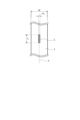
- FIG. 3 is a schematic diagram for explaining the position and dimensions of a measurement surface when performing composition analysis by AES.
- the bonding wire of the present invention (hereinafter, simply referred to as "the wire of the present invention” or “wire”) is A core material made of Cu or a Cu alloy; a coating layer formed on the surface of the core material, the coating layer having a total concentration of Pd and Ni of 90 atomic % or more; In a concentration profile in the depth direction of the wire obtained by measuring 50 or more measurement points in the coating layer by Auger electron spectroscopy (AES), The thickness of the coating layer is 10 nm or more and 130 nm or less, When the average value of the ratio C Pd /C Ni of the Pd concentration C Pd (atomic %) to the Ni concentration C Ni (atomic %) at all measurement points of the coating layer is X, the average value X is 0.1 or more and 35.0 or less, the total number of measurement points in the coating layer having an absolute deviation of 0.3X or less from the average value X is 50% or more of the total number of measurement points in the coating layer; It is characterized in that the
- bonding wires are required to have good bonding reliability in harsh high-temperature environments.
- bonding wires used in in-vehicle devices are required to have bonding reliability in high-temperature environments exceeding 150°C.
- the inventors conducted an evaluation based on the characteristics required in recent years and found that with a conventional Cu bonding wire having a Pd coating layer, galvanic corrosion occurs in high-temperature environments, and bonding reliability at the 2nd joint may not be sufficient.
- an alloy-coated Cu bonding wire includes a core material made of Cu or a Cu alloy, and a coating layer formed on the surface of the core material in which the total concentration of Pd and Ni is 90 atomic % or more, and in a concentration profile in the depth direction of the wire obtained by measuring the depth direction measurement points in the coating layer by AES so that there are 50 or more measurement points in the coating layer, the thickness of the coating layer is 10 nm or more and 130 nm or less, and when the average value of the ratio C Pd /C Ni of the Pd concentration C Pd (atomic %) and the Ni concentration C Ni (atomic %) for all measurement points in the coating layer is X, the average value X is 0.1 to 35.0, and the total number of measurement points in the coating layer that have an absolute deviation of 0.3X or less from the average value X is 50% or more of the total number of measurement points in the coating layer. This results in a good FAB shape, and suppresses galvanic corrosion in a high
- Fig. 1 shows a schematic diagram of the second bonding portion formed on the external terminal (not shown) as viewed from directly above in a direction perpendicular to the main surface of the external terminal.
- the second bonding portion 10 is formed at the tip of the wire 1.
- FIG. 2 shows a schematic cross-sectional view of the 2nd joint when cut in a direction perpendicular to the main surface of the external terminal at the position indicated by the two-dot chain line A-A in FIG. 1.
- the 2nd joint 10 is formed on the external terminal 50, but the inventors have found that the 2nd joint formed using the above alloy-coated Cu bonding wire tends to have areas where the wire and the external terminal are not adhered to each other within a certain width from the ends of the 2nd joint (the left and right ends of the 2nd joint 10 in FIG. 2).
- Such problems with the adhesion of the 2nd joint have not been apparent at least in conventional bonding wires, including bare Cu bonding wires, and are therefore considered to be a specific problem caused by the adoption of the above specific alloy coating.
- the inventors have discovered that by using the specific alloy coating and a bonding wire that satisfies the above condition (A), it is possible to improve the adhesion of the second joint and achieve good initial bonding of the second joint while retaining the excellent effects achieved by using the specific alloy coating.
- the wire of the present invention includes a core material made of Cu or a Cu alloy (hereinafter, also simply referred to as a "Cu core material").
- the Cu core material is not particularly limited as long as it is made of Cu or a Cu alloy, and any known Cu core material that constitutes a conventional Pd-coated Cu wire known as a bonding wire may be used.
- the concentration of Cu in the Cu core material can be, for example, 97 atomic % or more, 97.5 atomic % or more, 98 atomic % or more, 98.5 atomic % or more, 99 atomic % or more, 99.5 atomic % or more, 99.8 atomic % or more, 99.9 atomic % or more, or 99.95 atomic % or more at the center (axial core portion) of the Cu core material.
- the Cu core material contains the first additive element so as to satisfy the above condition (A).
- the Cu core material may also contain one or more dopants selected from, for example, the second, third, fourth, and fifth additive elements described below. The preferred contents of these dopants are as described below.
- the Cu core material is composed of Cu, a first additive element, and inevitable impurities.
- the Cu core material is composed of Cu, a first additive element, and one or more elements selected from a second additive element, a third additive element, a fourth additive element, and a fifth additive element described below, and inevitable impurities.
- the Cu core material may contain elements that constitute the coating layer described below.
- the wire of the present invention includes a coating layer (hereinafter simply referred to as "coating layer”) formed on the surface of a Cu core material, the coating layer having a total concentration of Pd and Ni of 90 atomic % or more.
- the coating layer in the wire of the present invention satisfies all of the following conditions (1) to (3) in the concentration profile in the depth direction of the wire obtained by AES measurement so that the number of measurement points in the depth direction in the coating layer is 50 or more (hereinafter simply referred to as the "concentration profile in the depth direction of the wire").
- the thickness of the coating layer is 10 nm or more and 130 nm or less.
- the average value of the ratio C Pd /C Ni of the Pd concentration C Pd (atomic %) to the Ni concentration C Ni (atomic %) at all measurement points of the coating layer is X
- the average value X is 0.1 or more and 35.0 or less.
- the total number of measurement points in the coating layer that have an absolute deviation of 0.3X or less from the average value X is 50% or more of the total number of measurement points in the coating layer.
- the measurement points in the depth direction are measured so that there are 50 or more points in the coating layer.
- AES can perform depth analysis at a measurement interval of the sub-nano order, it is relatively easy to set the measurement points to 50 or more points in relation to the thickness of the coating layer targeted by the present invention. If the number of measurement points is less than 50 points as a result of the measurement, the sputtering speed is lowered or the sputtering time is shortened so that the number of measurement points is 50 or more points, and the measurement is performed again.
- the measurement points in the depth direction are measured so that there are 50 or more points in the coating layer by AES, and the concentration profile in the depth direction of the wire can be obtained.
- the measurement point interval of AES it is more preferable to determine the measurement point interval of AES so that the total number of measurement points on the coating layer is 70 points (more preferably 100 points). Therefore, in a preferred embodiment, the coating layer of the wire of the present invention satisfies all of the above conditions (1) to (3) in the concentration profile in the depth direction of the wire obtained by measuring 50 or more points in the coating layer using AES.
- Condition (1) relates to the thickness of the coating layer.
- the wire of the present invention can suppress galvanic corrosion in a high-temperature environment, provide good bonding reliability of the second bonded portion, and provide a good FAB shape, and therefore a good crimped shape of the first bonded portion.
- the thickness of the coating layer (a calculation method based on the concentration profile in the depth direction of the wire will be described later) is 10 nm or more from the viewpoint of realizing a good FAB shape, preferably 12 nm or more, 14 nm or more, 15 nm or more, 16 nm or more, 18 nm or more, or 20 nm or more, more preferably 25 nm or more, 30 nm or more, 40 nm or more, or 50 nm or more, and even more preferably 60 nm or more, 70 nm or more, 80 nm or more, or 90 nm or more.
- the thickness of the coating layer is less than 10 nm, eccentricity occurs during FAB formation, the FAB shape deteriorates, and the crimp shape of the 1st joint tends to deteriorate.
- the upper limit of the thickness of the coating layer is 130 nm or less from the viewpoint of realizing a good FAB shape, and is preferably 125 nm or less, 120 nm or less, 115 nm or less, or 110 nm or less. If the coating layer is thicker than 130 nm, deformation or poor melting will occur during FAB formation, causing a deterioration in the FAB shape and a tendency for the compression shape of the first joint to deteriorate.
- the wire of the present invention can suppress galvanic corrosion in a high temperature environment to provide good bonding reliability of the 2nd bonded portion, and can also provide a good FAB shape and, ultimately, a good crimp shape of the 1st bonded portion.
- the average value X is 35.0 or less, preferably 34.0 or less, more preferably 32.0 or less, 30.0 or less, 28.0 or less, 26.0 or less, 25.0 or less, 24.0 or less, 22.0 or less, or 20.0 or less, from the viewpoint of realizing good joint reliability of the 2nd joint. If the ratio C Pd /C Ni is more than 35.0, galvanic corrosion in a high temperature environment cannot be suppressed, and there is a tendency that sufficient high temperature joint reliability cannot be obtained at the 2nd joint.
- the lower limit of the average value X is 0.1 or more, preferably 0.2 or more, 0.4 or more, 0.5 or more, 0.6 or more, 0.8 or more, 1.0 or more, or more than 1.0, more preferably 1.5 or more, 2.0 or more, 2.5 or more, or 3.0 or more, from the viewpoint of increasing the initial joint strength of the 2nd joint and realizing good initial jointability of the 2nd joint. If the average value X is less than 0.1, there is a tendency that sufficient initial bondability of the second bonded portion cannot be obtained.
- -Condition (3)- Condition (3) relates to the total number of measurement points in the coating layer having an absolute deviation of 0.3X or less from the average value X being 50% or more of the total number of measurement points in the coating layer.
- Condition (3) together with condition (2), indicates that the coating layer contains a high concentration of PdNi alloy, which contains Pd and Ni in a predetermined ratio, while suppressing fluctuations in the Pd/Ni ratio in the thickness direction of the coating layer. From the viewpoint of achieving better bonding reliability of the second bonding part in a high-temperature environment and from the viewpoint of achieving a better FAB shape, it is more preferable that the total number of measurement points in the coating layer whose absolute deviation from the average value X is within 0.2X (more preferably within 0.18X, 0.16X, or 0.15X) is 50% or more of the total number of measurement points in the coating layer.
- the total number of measurement points in the coating layer whose absolute deviation from the average value X is within a predetermined range is preferably 55% or more or 60% or more, more preferably 65% or more, 70% or more or 75% or more, and even more preferably 80% or more of the total number of measurement points in the coating layer.
- the difference between the maximum and minimum values of the approximate line in the depth (thickness) range of the coating layer is preferably 20 atomic % or less, more preferably 15 atomic % or less, and even more preferably 10 atomic % or less, 8 atomic % or less, 6 atomic % or less, or 5 atomic % or less.
- the average value X is less than 1, it is preferable that when C Ni (atomic %) is linearly approximated by the least squares method for all measurement points of the coating layer, the difference between the maximum and minimum values of the approximate line in the depth range of the coating layer is in the above range, and when the average value X is 1 or more, it is preferable that when C Pd (atomic %) is linearly approximated by the least squares method for all measurement points of the coating layer, the difference between the maximum and minimum values of the approximate line in the depth range of the coating layer is in the above range.
- the thickness of the coating layer under condition (1), the average value X and the absolute deviation from the average value X under conditions (2) and (3), the total number of measurement points where the absolute deviation is within a predetermined range, and the ratio of the total number of measurement points where the absolute deviation is within a predetermined range to the total number of measurement points of the coating layer can be confirmed and determined by performing composition analysis by AES while digging in the depth direction (direction toward the center of the wire) from the surface of the wire by Ar sputtering.
- the concentration change of each element in the depth (center) direction from the surface of the wire can be obtained, and the concentration profile can be confirmed and determined based on the concentration profile.
- the unit of depth is SiO2 conversion when obtaining the concentration profile in the depth direction.
- FIG. 3 is a schematic plan view of the wire 1, in which the direction of the wire axis (wire length direction) corresponds to the vertical direction (up and down direction) of FIG. 3, and the direction perpendicular to the wire axis (wire thickness direction) corresponds to the horizontal direction (left and right direction) of FIG.
- FIG. 3 shows the measurement surface 2 in relation to the wire 1, where the width of the measurement surface 2 is the dimension w a of the measurement surface in the direction perpendicular to the wire axis, and the length of the measurement surface 2 is the dimension l a of the measurement surface in the direction of the wire axis.
- the center of the wire width in the direction perpendicular to the wire axis is positioned to be the center of the width of the measurement surface, and the measurement surface is determined so that the width of the measurement surface is 5% to 15% of the wire diameter.
- the length of the measurement surface is set to be 5 times the width of the measurement surface.
- the width of the wire is indicated by the symbol W, and the center of the width of the wire is indicated by the dashed line X.
- the measurement surface 2 is positioned so that the center of its width coincides with the dashed line X which is the center of the wire width, and the width w a of the measurement surface is determined to be 5% to 15% of the wire diameter (same value as the width W of the wire), that is, 0.05W to 0.15W.
- the thickness of the coating layer under condition (1) above, the average value X and the absolute deviation from the average value X under conditions (2) and (3), the total number of measurement points where the absolute deviation is within a specified range, and the ratio of the total number of measurement points of the coating layer where the absolute deviation is within a specified range to the total number of measurement points are based on the results of measurements under the conditions described in the [Analysis of coating layer thickness by Auger electron spectroscopy (AES)] section below.
- the concentrations of Pd and Ni tend to decrease and the concentration of Cu tends to increase.
- the thickness of the coating layer and the total number of measurement points of the coating layer can be obtained from the thickness of the region in which the total concentration of Pd and Ni is 90 atomic % or more and the total number of measurement points, focusing on the concentration of Pd C Pd (atomic %) and the concentration of Ni C Ni (atomic %).
- the average value X can be obtained by arithmetically averaging the ratios C Pd /C Ni for all the measurement points of the coating layer, and the total number of measurement points whose absolute deviation from the average value X is within 0.3X can be obtained by checking the absolute deviation from the average value X for all the measurement points of the coating layer.
- the Au concentration tends to decrease and the Pd and Ni concentrations tend to increase from the surface of the wire to a very shallow position in the concentration profile in the depth direction.
- the thickness of the coating layer and the total number of measurement points of the coating layer can be obtained from the thickness of the region where the total is 90 atomic % or more and the total number of measurement points, focusing on the Pd concentration C Pd (atomic %) and the Ni concentration C Ni (atomic %), and the average value X can be obtained by arithmetically averaging the ratios C Pd /C Ni for all the measurement points of the coating layer, and the total number of measurement points whose absolute deviation from the average value X is within 0.3X can be obtained by checking the absolute deviation from the average value X for all the measurement points of the coating layer.
- the coating layer-- In the wire of the present invention, in addition to satisfying all of the above conditions (1) to (3), it is more preferable that the coating layer satisfies one or both of the following conditions (4) and (5) based on the concentration profile in the depth direction of the wire.
- the average value of the Pd concentration C Pd (atomic%) for all measurement points of the coating layer is X Pd
- the total number of measurement points in the coating layer that have an absolute deviation from the average value X Pd of 0.1X Pd or less is 50% or more of the total number of measurement points of the coating layer.
- the wire of the present invention can provide particularly good joint reliability of the 2nd joint in a high temperature environment and achieve a particularly good FAB shape.
- the coating layer may contain, for example, one or more dopants selected from the second, third, fourth, and fifth additional elements described below. The preferred contents of these dopants are as described below.
- the wire of the present invention may further contain Au on its surface.
- the initial bondability of the 2nd bonded portion can be further improved.
- the concentration of Au relative to the entire wire may be usually 0.5 mass% or less, preferably 0.3 mass% or less or 0.2 mass% or less, and the lower limit may be, for example, 0.05 mass% or more, 0.1 mass% or more, etc. Therefore, in one embodiment, the wire of the present invention satisfies the following condition (B).
- the surface of the wire contains Au, and the concentration of Au in the entire wire is 0.5 mass % or less.
- the wire of the present invention further contains Au on its surface, in determining whether the above condition (A) is met, the concentration of Au as the first additive element is the concentration in the core portion, determined by exposing the cross section of the wire and measuring the Cu core portion with an electron probe microanalyzer (EPMA) or secondary ion mass spectrometry (SIMS).
- EPMA electron probe microanalyzer
- SIMS secondary ion mass spectrometry
- the wire of the present invention includes a coating layer that satisfies the above conditions (1) to (3) and also satisfies the following conditions (A) and (B).
- the wire contains one or more elements ("first additive elements") selected from the group consisting of Ti, V, Cr, Mn, Fe, Co, Zn, Zr, Nb, Mo, Ru, Rh, Sn, Ta, W, Os, Ir, Pt, Au, and Bi, and the total concentration of the first additive elements in the entire wire (wherein the concentration of Au is the concentration in the core material portion) is 5 ppm by mass or more and 450 ppm by mass or less.
- the wire contains Au on the surface thereof, and the concentration of Au in the entire wire is 0.5% by mass or less.
- the alloy-coated Cu bonding wire of the present invention which contains the first additive element at the above-mentioned specific concentration, can improve the adhesion of the second joint and achieve good initial bondability of the second joint even when the Au concentration on the wire surface is low, for example, less than 10 atomic %, 8 atomic % or less, 6 atomic % or less, 5 atomic % or less, 4 atomic % or less, or 2 atomic % or less.
- compositional analysis of the wire surface can be performed under the same conditions as 1) the compositional analysis of the wire surface, which was explained in relation to the method for obtaining a concentration profile in the depth direction. That is, when performing compositional analysis of the wire surface by Auger electron spectroscopy (AES), the position and dimensions of the measurement surface are determined as follows.
- AES Auger electron spectroscopy
- the wire is positioned so that the center of the wire width in the direction perpendicular to the wire axis is the center of the width of the measurement surface, and the measurement surface is determined so that the width of the measurement surface is 5% to 15% of the wire diameter.
- the length of the measurement surface is set to be 5 times the width of the measurement surface.
- the boundary between the Cu core material and the coating layer is determined based on the total concentration of Pd and Ni in the concentration profile in the depth direction of the wire.
- the position where the total concentration of Pd and Ni is 90 atomic % is determined to be the boundary, and the region where the total concentration of Pd and Ni is less than 90 atomic % is the Cu core material, and the region where it is 90 atomic % or more is the coating layer.
- the boundary between the Cu core material and the coating layer does not necessarily have to be a grain boundary.
- the thickness of the coating layer can be determined by checking the concentration profile from the wire surface toward the center of the wire, and is the distance from depth position Z1 where the total concentration of Pd and Ni first reaches 90 atomic % or more to depth position Z2 where the total concentration of Pd and Ni first falls below 90 atomic % (where Z2 > Z1).
- the wire of the present invention is characterized in that it includes a coating layer that satisfies the above conditions (1) to (3), but the average value X and absolute deviation from the average value X related to conditions (2) and (3), the total number of measurement points where the absolute deviation is within a predetermined range, and the ratio of the total number of measurement points where the absolute deviation is within a predetermined range to the total number of measurement points in the coating layer are determined with focus on the Pd concentration C Pd (atomic %) and the Ni concentration C Ni (atomic %) for the coating layer determined by the above-mentioned boundary judgment method.
- the coating layer is made of Pd and Ni; unavoidable impurities.
- the coating layer is made of Pd and Ni; one or more elements selected from Au and the first additional element; and unavoidable impurities.
- the coating layer is made of Pd and Ni; one or more elements selected from the second additional element, the third additional element, the fourth additional element, and the fifth additional element described below; and unavoidable impurities.
- the coating layer is made of Pd and Ni; one or more elements selected from Au and the first additional element; one or more elements selected from the second additional element, the third additional element, the fourth additional element, and the fifth additional element described below; and unavoidable impurities.
- the coating layer may contain the elements that make up the Cu core material described above.
- the wire of the present invention is characterized in that it satisfies the following condition (A).
- A Contains one or more elements ("first additive elements") selected from the group consisting of Ti, V, Cr, Mn, Fe, Co, Zn, Zr, Nb, Mo, Ru, Rh, Sn, Ta, W, Os, Ir, Pt, Au, and Bi, and the total concentration of the first additive elements in the entire wire is 5 ppm by mass or more and 450 ppm by mass or less.
- the wire of the present invention provides a good FAB shape and good bonding reliability of the second joint in a high-temperature environment, and can improve the adhesion of the second joint to achieve good initial bonding of the second joint.
- Condition (A) relates to the total concentration of one or more elements selected from the group consisting of Ti, V, Cr, Mn, Fe, Co, Zn, Zr, Nb, Mo, Ru, Rh, Sn, Ta, W, Os, Ir, Pt, Au, and Bi, i.e., the first additive element, in the entire wire.
- the wire of the present invention further contains Au on its surface, the "total concentration of the first additive element in the entire wire” in condition (A) should be read as the “total concentration of the first additive element in the entire wire (however, the concentration of Au is the concentration in the core material).
- the total concentration of the first additive element in the entire wire is 5 mass ppm or more, preferably 10 mass ppm or more, 15 mass ppm or more, 20 mass ppm or more, or 25 mass ppm or more, more preferably 30 mass ppm or more, 40 mass ppm or more, 50 mass ppm or more, 60 mass ppm or more, or 80 mass ppm or more, and even more preferably 100 mass ppm or more, 110 mass ppm or more, 120 mass ppm or more, 130 mass ppm or more, 140 mass ppm or more, or 150 mass ppm or more.
- the total concentration of the first additive element in the entire wire is 100 mass ppm or more, this is preferable because it improves the adhesion of the second joint and makes it easier to realize a bonding wire that provides better initial bonding of the second joint.
- the total concentration of the first additive element is 450 mass ppm or less for the entire wire.
- the upper limit of the total concentration of the first additive element may be 440 mass ppm or less, 420 mass ppm or less, 400 mass ppm or less, etc.
- the first additive element includes one or more elements selected from the group consisting of Ti, V, Cr, Mn, Fe, Co, and Zn (hereinafter also referred to as "1a additive element")
- the upper limit of the total concentration of the 1a additive element may be 200 mass ppm or less, 180 mass ppm or less, 160 mass ppm or less, or 150 mass ppm or less, etc.
- the upper limit of the total concentration of the 1b additional element may be 350 ppm by mass or less, 340 ppm by mass or less, 320 ppm by mass or less, or 300 ppm by mass or less.
- the first additive element is contained in the Cu core material.
- the wire of the present invention may further contain one or more elements ("second additive elements") selected from the group consisting of B, P and Mg.
- second additive elements selected from the group consisting of B, P and Mg.
- the total concentration of the second additive element in the entire wire is preferably 1 mass ppm or more. This makes it possible to realize a bonding wire that provides a better crimp shape of the 1st joint.
- the total concentration of the second additive element in the entire wire is more preferably 2 mass ppm or more, and even more preferably 3 mass ppm or more, 5 mass ppm or more, 8 mass ppm or more, 10 mass ppm or more, 15 mass ppm or more or 20 mass ppm or more.
- the total concentration of the second additive element is preferably 100 mass ppm or less, and more preferably 90 mass ppm or less, 80 mass ppm or less, 70 mass ppm or less, 60 mass ppm or less or 50 mass ppm or less. Therefore, in a preferred embodiment, the wire of the present invention contains a second additive element, and the total concentration of the second additive element in the entire wire is 1 ppm by mass or more and 100 ppm by mass or less.
- the second additive element may be contained in either the Cu core material or the coating layer, or may be contained in both. From the viewpoint of realizing a bonding wire that provides a better crimp shape of the first joint, it is preferable that the second additive element is contained in the Cu core material.
- the wire of the present invention may further contain one or more elements ("third additive elements") selected from the group consisting of Se, Te, As and Sb.
- third additive elements selected from the group consisting of Se, Te, As and Sb.
- the total concentration of the third additive element in the entire wire is preferably 1 mass ppm or more. This can improve the bonding reliability of the 1st joint in a high-temperature and high-humidity environment.
- the total concentration of the third additive element in the entire wire is more preferably 2 mass ppm or more, and even more preferably 3 mass ppm or more, 5 mass ppm or more, 8 mass ppm or more, 10 mass ppm or more, 15 mass ppm or more or 20 mass ppm or more.
- the total concentration of the third additive element is preferably 100 mass ppm or less, and more preferably 90 mass ppm or less, 80 mass ppm or less, 70 mass ppm or less, 60 mass ppm or less or 50 mass ppm or less. Therefore, in a preferred embodiment, the wire of the present invention contains a third additive element, and the total concentration of the third additive element in the entire wire is 1 ppm by mass or more and 100 ppm by mass or less.
- the third additive element may be contained in either the Cu core material or the coating layer, or may be contained in both. From the viewpoint of realizing a bonding wire that provides even better bonding reliability of the first bonding portion in a high-temperature, high-humidity environment, it is preferable that the third additive element is contained in the coating layer.
- the wire of the present invention may further contain one or more elements ("fourth additive element") selected from the group consisting of Ga and Ge.
- fourth additive element selected from the group consisting of Ga and Ge.
- the total concentration of the fourth additive element in the entire wire is preferably 0.011 mass% or more. This can improve the bonding reliability of the 1st bonding portion in a high-temperature environment.
- the total concentration of the fourth additive element in the entire wire is more preferably 0.015 mass% or more, and even more preferably 0.02 mass% or more, 0.025 mass% or more, 0.03 mass% or more, 0.031 mass% or more, 0.035 mass% or more, 0.04 mass% or more, 0.05 mass% or more, 0.07 mass% or more, 0.09 mass% or more, 0.1 mass% or more, 0.12 mass% or more, 0.14 mass% or more, 0.15 mass% or more, or 0.2 mass% or more.
- the total concentration of the fourth additive element is preferably 1.5 mass% or less, and more preferably 1.4 mass% or less, 1.3 mass% or less, or 1.2 mass% or less. Therefore, in a preferred embodiment, the wire of the present invention contains a fourth additive element, and the total concentration of the fourth additive element in the entire wire is 0.011 mass% or more and 1.5 mass% or less.
- the fourth additive element may be contained in either the Cu core material or the coating layer, or in both.
- the wire of the present invention may further contain one or more elements selected from the group consisting of In and Ag ("fifth additive element").
- the wire of the present invention contains the fifth additive element, the total concentration of the fifth additive element in the entire wire is preferably 1 mass ppm or more. This can provide good bonding reliability of the 2nd joint even in a harsher high-temperature environment (e.g., 200°C).
- the total concentration of the fifth additive element in the entire wire is preferably 2 mass ppm or more, 3 mass ppm or more, 4 mass ppm or more, or 5 mass ppm or more, more preferably 6 mass ppm or more, 8 mass ppm or more, or 10 mass ppm or more, even more preferably 20 mass ppm or more, 30 mass ppm or more, or 40 mass ppm or more, and even more preferably 50 mass ppm or more, 60 mass ppm or more, or 70 mass ppm or more.
- the upper limit of the concentration of the fifth additive element in the entire wire may be, for example, 500 mass ppm or less, 480 mass ppm or less, 460 mass ppm or less, 450 mass ppm or less, etc., taking into consideration costs, etc., since the effect of improving the joint reliability of the 2nd joint in a high-temperature environment reaches a plateau even if the fifth additive element is contained in a higher amount. Therefore, in a preferred embodiment, the wire of the present invention contains the fifth additive element, and the total concentration of the fifth additive element in the entire wire is 1 mass ppm or more and 500 mass ppm or less.
- the fifth additive element may be contained in either the Cu core material or the coating layer, or may be contained in both. From the viewpoint of realizing a bonding wire that exhibits good bonding reliability of the second joint in a harsh high-temperature environment, it is preferable that the fifth additive element is contained in the Cu core material.
- the contents of the first, second, third, fourth, and fifth added elements in the wire can be measured by the method described below in [Measurement of element contents].
- the total concentration of Cu, Ni, and Pd can be, for example, 98.5 mass% or more, 98.6 mass% or more, 98.7 mass% or more, or 98.8 mass% or more.
- the diameter of the wire of the present invention is not particularly limited and may be determined appropriately depending on the specific purpose, but is preferably 13 ⁇ m or more, 15 ⁇ m or more, 18 ⁇ m or more, or 20 ⁇ m or more.
- the upper limit of the diameter is not particularly limited and may be, for example, 80 ⁇ m or less, 70 ⁇ m or less, or 50 ⁇ m or less.
- the wire of the present invention not only provides a good FAB shape, but also has good initial bonding properties at the second joint, including adhesion at the second joint, and can suppress galvanic corrosion in high-temperature environments to provide good bonding reliability at the second joint. Therefore, the bonding wire of the present invention can be suitably used to connect between electrodes on a semiconductor chip and external terminals such as electrodes on a lead frame or substrate.
- the raw copper used has a purity of 4N (99.99% by mass or higher) or higher, and ingots containing each dopant are obtained using the method described below.
- Methods of adding dopants such as the above-mentioned first additive element and, if added, the second, third, fourth, and fifth additive elements include, for example, a method of including them in the Cu core material, a method of including them in the coating layer, a method of depositing them on the surface of the Cu core material, a method of depositing them on the surface of the coating layer, and combinations of these methods, and these methods can be selected appropriately.
- the dopant component may be added directly to Cu, or a mother alloy containing about a few percent of the dopant component may be used.
- the dopant may be included in a Pd or Ni plating bath (in the case of wet plating) or in a target material (in the case of dry plating) when forming the coating layer.
- a Pd or Ni plating bath in the case of wet plating
- a target material in the case of dry plating
- the surface of the Cu core material or the surface of the coating layer is used as the deposition surface, and one or more deposition processes selected from (1) application of an aqueous solution ⁇ drying ⁇ heat treatment, (2) plating method (wet type), and (3) vapor deposition method (dry type) are carried out.
- intermediate wire made of Cu or Cu alloy and having a diameter of approximately 0.7 to 2.0 mm.
- the method of forming a coating layer on the surface of the Cu core material can be electrolytic plating, electroless plating, vapor deposition, etc., but electrolytic plating, which can stably control the film thickness, is industrially preferable.
- a coating layer may be formed on the surface of the intermediate wire.
- the coating layer may also be applied at the ingot stage, or the coating layer may be formed on the surface of the Cu core material after the intermediate wire is drawn and further thinned (for example, after drawing to the final wire diameter).
- the coating layer may be formed, for example, by providing a PdNi alloy layer containing Pd and Ni in a predetermined ratio on the surface of the Cu core material, or, from the viewpoint of forming a coating layer with excellent adhesion to the Cu core material, by providing a PdNi alloy layer containing Pd and Ni in a predetermined ratio after strike plating of a conductive metal on the surface of the Cu core material.
- a layer containing one or more of Pd and Ni e.g., a Pd layer, a Ni layer, a PdNi alloy layer
- a layer containing one or more of Pd and Ni may be further provided.
- a wire containing Au When forming a wire containing Au on its surface, it can be formed by providing an Au layer on the surface of the coating layer using a method similar to that described above.
- the wire is drawn to the final wire diameter (approximately 13 to 80 ⁇ m in diameter) using a wire drawing device with diamond dies.
- intermediate heat treatment may also be performed during the wire drawing process.
- a semiconductor device can be manufactured by using the semiconductor device bonding wire of the present invention to connect electrodes on a semiconductor chip to external terminals such as electrodes on a lead frame or a circuit board.
- the semiconductor device of the present invention includes a circuit board, a semiconductor chip, and a bonding wire for electrically connecting the circuit board and the semiconductor chip, the bonding wire being the wire of the present invention.
- the circuit board and semiconductor chip are not particularly limited, and any known circuit board and semiconductor chip that can be used to configure a semiconductor device may be used.
- a lead frame may be used instead of a circuit board.
- the semiconductor device may be configured to include a lead frame and a semiconductor chip mounted on the lead frame, as in the semiconductor device described in JP 2020-150116 A.
- Semiconductor devices include various semiconductor devices used in electrical products (e.g., computers, mobile phones, digital cameras, televisions, air conditioners, solar power generation systems, etc.) and vehicles (e.g., motorcycles, automobiles, trains, ships, aircraft, etc.).
- electrical products e.g., computers, mobile phones, digital cameras, televisions, air conditioners, solar power generation systems, etc.
- vehicles e.g., motorcycles, automobiles, trains, ships, aircraft, etc.
- the raw material Cu used had a purity of 4N (99.99% by mass or more) or higher.
- the first additive element, and the second, third, fourth, and fifth additive elements, if added, had a purity of 3N or higher, or the mother alloy contained a few percent of these additive elements in Cu.
- the Cu alloy core material was first loaded into a graphite crucible, heated to 1090-1800°C in an inert atmosphere of N2 gas or Ar gas, etc., using a high-frequency furnace, and melted, and then an ingot with a diameter of 3-6 mm was produced by continuous casting. Next, the obtained ingot was subjected to wire drawing to produce an intermediate wire with a diameter of 0.7-2.0 mm. In the wire drawing, a commercially available lubricating liquid was used, and the wire drawing speed was set to 20-150 m/min. The coating layer was formed by electrolytic plating. Some of the wires (Example Nos. 5, 9, 15, 27, 33, and 36) had an Au layer on the PdNi alloy layer. As for the plating solution, a Pd-Ni plating solution and an Au plating solution were prepared and appropriately adjusted.
- Test and Evaluation Methods The test and evaluation methods are described below.
- the concentration of Au on the wire surface was determined by measuring the wire surface as the measurement surface by Auger electron spectroscopy (AES) as follows. First, the bonding wire to be measured was fixed linearly to the sample holder. Next, the wire was positioned so that the center of the width of the wire in the direction perpendicular to the wire axis was the center of the width of the measurement surface, and the measurement surface was determined so that the width of the measurement surface was 5% to 15% of the wire diameter. The length of the measurement surface was set to 5 times the width of the measurement surface.
- composition analysis of the wire surface was performed under the condition of an acceleration voltage of 10 kV, and the surface Au concentration (atomic %) was obtained.
- the composition analysis by AES was performed on three measurement surfaces separated by 1 mm or more in the wire axial direction, and the arithmetic average value was used.
- gas components such as carbon (C), sulfur (S), oxygen (O), and nitrogen (N), and nonmetallic elements were not taken into consideration.
- the thickness of the coating layer was analyzed by depth analysis using AES.
- the AES depth analysis is a method for analyzing the change in composition in the depth direction by alternately performing composition analysis and sputtering, and can obtain the concentration change of each element in the depth direction (center) from the wire surface (so-called concentration profile in the depth direction). Specifically, 1) the composition of the wire surface was analyzed by AES, and then 2) sputtering with Ar and 3) the composition of the surface after sputtering were repeated to obtain a concentration profile in the depth direction. The sputtering in 2) was performed with Ar + ions and an acceleration voltage of 2 kV.
- composition analysis of the surface in 1) and 3 the conditions for the dimensions of the measurement surface, the composition analysis by AES, and the calculation of the concentration of each element were the same as those described in the above [Composition analysis of wire surface by Auger electron spectroscopy (AES)] section.
- AES Auger electron spectroscopy
- the concentration profile was confirmed from the wire surface toward the wire center, and the distance from the depth position Z1 where the sum of the Pd concentration C Pd (atomic %) and the Ni concentration C Ni (atomic %) first reached 90 atomic % or more to the depth position Z2 (where Z2>Z1) where the sum of C Pd and C Ni first dropped to less than 90 atomic % was obtained as the measured thickness of the coating layer.
- the total number of measurement points from the depth position Z1 to the depth position Z2 was obtained as the total number of measurement points of the coating layer.
- the thickness of the coating layer was the arithmetic average value of the numerical values obtained for the three measurement surfaces. In addition, it was confirmed that the total number of measurement points of the coating layer was 50 to 100 points for the wire of the embodiment.
- the depth measured by AES analysis is calculated as the product of the sputtering rate and time. Since the sputtering rate is generally measured using a standard sample of SiO2 , the depth analyzed by AES is a SiO2 equivalent value. In other words, the SiO2 equivalent value is used as the unit of the thickness of the coating layer.
- the ratio C Pd /C Ni of the Pd concentration C Pd (atomic%) and the Ni concentration C Ni (atomic%) for all measurement points of the coating layer was arithmetically averaged to obtain the average value X.
- the absolute deviation from the average value X was calculated for the ratio C Pd /C Ni of all measurement points of the coating layer, and the total number of measurement points whose absolute deviation from the average value X was within 0.3X and the total number of measurement points whose absolute deviation from the average value X was within 0.2X were obtained.
- the average value X was the arithmetic average value of the values obtained for the three measurement surfaces.
- the contents of the first, second, third, fourth, and fifth additive elements in the wire were detected as the concentration of the elements contained in the entire wire by analyzing a liquid obtained by dissolving the bonding wire in strong acid using an ICP optical emission spectrometer and an ICP mass spectrometer.
- an ICP-OES PS3520UVDDII
- an ICP-MS ICP-MS
- the concentration of Au as the first additive element was obtained by exposing the cross section of the wire and measuring the Cu core part by an electron beam microanalyzer (EPMA) or secondary ion mass spectrometry (SIMS).
- EPMA electron beam microanalyzer
- SIMS secondary ion mass spectrometry
- the FAB was formed with a current value of 30-75 mA, an EFO gap of 762 ⁇ m, a tail length of 254 ⁇ m, and N 2 +5% H 2 gas flowing at a flow rate of 0.4-0.6 L/min, and the diameter was set to 1.5-1.9 times the wire diameter.
- the FAB shape was judged as good if it was perfectly spherical, and bad if it had eccentricity, irregular shape, or poor melting. Evaluation was performed according to the following criteria.
- the initial bondability of the second bonded portion was evaluated by measuring and observing the bond strength and adhesion of the second bonded portion. In detail, the bond strength of the second bonded portion was measured by a pull test. The adhesion of the second bonded portion was evaluated by observing the cross section of the second bonded portion with a SEM.
- the width of the 2nd joint refers to the dimension in the left-right direction of the 2nd joint 10 in FIG. 1, and the cross section polishing by the ion beam was performed in a direction perpendicular to the straight line passing through the center X of the width of the wire in FIG. 1 (along the two-dot chain line A-A in FIG. 1) at a position where the width of the 2nd joint is approximately maximum.
- the resulting second joint was evaluated according to the following criteria based on its bond strength (pull strength) and adhesion (adhesion rate).
- a sample was prepared for testing the bonding reliability of the 2nd bonding part by wedge bonding using a commercially available wire bonder on the lead part of the lead frame and sealing it with a commercially available thermosetting epoxy resin.
- a Cu alloy lead frame with 1-3 ⁇ m Ag plating was used as the lead frame.
- the prepared sample for evaluating the bonding reliability was exposed to an environment at a temperature of 175°C using a high-temperature thermostat.
- the bonding life of the 2nd bonding part was determined by conducting a pull test on the wedge bonding part every 500 hours and determining the time when the pull strength value became 1/2 of the initial pull strength.
- the arithmetic average value of the measured values of 50 randomly selected points on the wedge bonding part was used for the pull strength value.
- the pull test after the high-temperature storage test was conducted after removing the resin by acid treatment to expose the wedge bonding part. Evaluation was then performed according to the following criteria.
- Bonding life is 3000 hours or more ⁇ : Bonding life is 2000 hours or more and less than 3000 hours ⁇ : Bonding life is 1000 hours or more and less than 2000 hours ⁇ : Bonding life is less than 1000 hours
- -HTSL- A sample was made by forming a 1.5 ⁇ m thick film of an alloy of Al-1.0 mass% Si-0.5 mass% Cu on a silicon substrate on a general metal frame, and ball-bonding the sample to the electrode using a commercially available wire bonder. The sample was sealed with a commercially available thermosetting epoxy resin to prepare a sample for a bonding reliability test of the 1st bonding part. The ball was formed under the conditions described in the above [FAB shape] column. The prepared sample for evaluating bonding reliability was exposed to an environment at a temperature of 175° C. using a high-temperature thermostat.
- the bonding life of the 1st bonding part was determined as the time when the shear strength value became 1/2 of the initial shear strength value by performing a shear test on the ball bonding part every 500 hours.
- the value of the shear strength was the arithmetic average value of the measured values of 50 randomly selected ball bonding parts.
- the shear test after the high-temperature storage test was performed after removing the resin by acid treatment to expose the ball bonding part. Then, it was evaluated according to the following criteria.
- Bonding life is 2000 hours or more.
- Bonding life is 1000 hours or more but less than 2000 hours.
- Bonding life is less than 1000 hours.
- Bonding life is 384 hours or more.
- Bonding life is 240 hours or more but less than 384 hours.
- Bonding life is less than 240 hours.
Landscapes
- Engineering & Computer Science (AREA)
- Mechanical Engineering (AREA)
- Wire Bonding (AREA)
Priority Applications (7)
| Application Number | Priority Date | Filing Date | Title |
|---|---|---|---|
| KR1020257001572A KR20260003646A (ko) | 2023-05-30 | 2023-06-27 | 본딩 와이어 |
| CN202380017072.4A CN119452459A (zh) | 2023-05-30 | 2023-06-27 | 接合线 |
| JP2023539793A JP7494400B1 (ja) | 2023-05-30 | 2023-06-27 | ボンディングワイヤ |
| EP23932298.5A EP4495982A4 (en) | 2023-05-30 | 2023-06-27 | BOND WIRE |
| US18/855,536 US12290883B2 (en) | 2023-05-30 | 2023-06-27 | Bonding wire |
| KR1020247023494A KR102758326B1 (ko) | 2023-05-30 | 2023-06-27 | 본딩 와이어 |
| JP2024083026A JP2024173736A (ja) | 2023-05-30 | 2024-05-22 | ボンディングワイヤ |
Applications Claiming Priority (2)
| Application Number | Priority Date | Filing Date | Title |
|---|---|---|---|
| JP2023-088808 | 2023-05-30 | ||
| JP2023088808 | 2023-05-30 |
Publications (1)
| Publication Number | Publication Date |
|---|---|
| WO2024247286A1 true WO2024247286A1 (ja) | 2024-12-05 |
Family
ID=93258829
Family Applications (1)
| Application Number | Title | Priority Date | Filing Date |
|---|---|---|---|
| PCT/JP2023/023777 Ceased WO2024247286A1 (ja) | 2023-05-30 | 2023-06-27 | ボンディングワイヤ |
Country Status (7)
| Country | Link |
|---|---|
| US (1) | US12290883B2 (cg-RX-API-DMAC7.html) |
| EP (1) | EP4495982A4 (cg-RX-API-DMAC7.html) |
| JP (2) | JP7494400B1 (cg-RX-API-DMAC7.html) |
| KR (1) | KR102758326B1 (cg-RX-API-DMAC7.html) |
| CN (1) | CN119452459A (cg-RX-API-DMAC7.html) |
| TW (2) | TW202523865A (cg-RX-API-DMAC7.html) |
| WO (1) | WO2024247286A1 (cg-RX-API-DMAC7.html) |
Families Citing this family (1)
| Publication number | Priority date | Publication date | Assignee | Title |
|---|---|---|---|---|
| CN120870208A (zh) * | 2025-09-11 | 2025-10-31 | 上海万生合金材料有限公司 | 腐蚀法分析靶覆盖率的方法 |
Citations (9)
| Publication number | Priority date | Publication date | Assignee | Title |
|---|---|---|---|---|
| JPS6148543A (ja) | 1984-08-10 | 1986-03-10 | Sumitomo Electric Ind Ltd | 半導体素子結線用銅合金線 |
| JP2005167020A (ja) | 2003-12-03 | 2005-06-23 | Sumitomo Electric Ind Ltd | ボンディングワイヤーおよびそれを使用した集積回路デバイス |
| WO2011129256A1 (ja) * | 2010-04-14 | 2011-10-20 | タツタ電線株式会社 | ボンディングワイヤ |
| JP2013131654A (ja) * | 2011-12-21 | 2013-07-04 | Tanaka Electronics Ind Co Ltd | Pd被覆銅ボールボンディングワイヤ |
| WO2017013796A1 (ja) | 2015-07-23 | 2017-01-26 | 日鉄住金マイクロメタル株式会社 | 半導体装置用ボンディングワイヤ |
| WO2017221770A1 (ja) | 2016-06-20 | 2017-12-28 | 日鉄住金マイクロメタル株式会社 | 半導体装置用銅合金ボンディングワイヤ |
| JP2018503743A (ja) | 2014-12-22 | 2018-02-08 | ヘレウス マテリアルズ シンガポール ピーティーイー. リミテッド | ニッケルを含む耐食性および耐湿性銅系ボンディングワイヤ |
| JP2020150116A (ja) | 2019-03-13 | 2020-09-17 | ルネサスエレクトロニクス株式会社 | 半導体装置およびその製造方法 |
| JP7157279B1 (ja) * | 2021-06-25 | 2022-10-19 | 日鉄マイクロメタル株式会社 | 半導体装置用ボンディングワイヤ |
Family Cites Families (4)
| Publication number | Priority date | Publication date | Assignee | Title |
|---|---|---|---|---|
| KR20060090700A (ko) | 2003-10-20 | 2006-08-14 | 스미토모덴키고교가부시키가이샤 | 본딩와이어 및 그것을 사용한 집적회로 디바이스 |
| SG11201604432SA (en) * | 2015-06-15 | 2017-01-27 | Nippon Micrometal Corp | Bonding wire for semiconductor device |
| DE112017000346T5 (de) | 2017-12-28 | 2019-08-29 | Nippon Micrometal Corporation | Bonddraht für Halbleiterbauelement |
| CN118712163A (zh) * | 2021-06-25 | 2024-09-27 | 日铁新材料股份有限公司 | 半导体装置用接合线 |
-
2023
- 2023-06-27 JP JP2023539793A patent/JP7494400B1/ja active Active
- 2023-06-27 EP EP23932298.5A patent/EP4495982A4/en active Pending
- 2023-06-27 WO PCT/JP2023/023777 patent/WO2024247286A1/ja not_active Ceased
- 2023-06-27 KR KR1020247023494A patent/KR102758326B1/ko active Active
- 2023-06-27 US US18/855,536 patent/US12290883B2/en active Active
- 2023-06-27 CN CN202380017072.4A patent/CN119452459A/zh active Pending
- 2023-06-30 TW TW114103873A patent/TW202523865A/zh unknown
- 2023-06-30 TW TW112124502A patent/TWI872591B/zh active
-
2024
- 2024-05-22 JP JP2024083026A patent/JP2024173736A/ja active Pending
Patent Citations (9)
| Publication number | Priority date | Publication date | Assignee | Title |
|---|---|---|---|---|
| JPS6148543A (ja) | 1984-08-10 | 1986-03-10 | Sumitomo Electric Ind Ltd | 半導体素子結線用銅合金線 |
| JP2005167020A (ja) | 2003-12-03 | 2005-06-23 | Sumitomo Electric Ind Ltd | ボンディングワイヤーおよびそれを使用した集積回路デバイス |
| WO2011129256A1 (ja) * | 2010-04-14 | 2011-10-20 | タツタ電線株式会社 | ボンディングワイヤ |
| JP2013131654A (ja) * | 2011-12-21 | 2013-07-04 | Tanaka Electronics Ind Co Ltd | Pd被覆銅ボールボンディングワイヤ |
| JP2018503743A (ja) | 2014-12-22 | 2018-02-08 | ヘレウス マテリアルズ シンガポール ピーティーイー. リミテッド | ニッケルを含む耐食性および耐湿性銅系ボンディングワイヤ |
| WO2017013796A1 (ja) | 2015-07-23 | 2017-01-26 | 日鉄住金マイクロメタル株式会社 | 半導体装置用ボンディングワイヤ |
| WO2017221770A1 (ja) | 2016-06-20 | 2017-12-28 | 日鉄住金マイクロメタル株式会社 | 半導体装置用銅合金ボンディングワイヤ |
| JP2020150116A (ja) | 2019-03-13 | 2020-09-17 | ルネサスエレクトロニクス株式会社 | 半導体装置およびその製造方法 |
| JP7157279B1 (ja) * | 2021-06-25 | 2022-10-19 | 日鉄マイクロメタル株式会社 | 半導体装置用ボンディングワイヤ |
Non-Patent Citations (1)
| Title |
|---|
| See also references of EP4495982A4 |
Also Published As
| Publication number | Publication date |
|---|---|
| JP7494400B1 (ja) | 2024-06-03 |
| KR102758326B1 (ko) | 2025-01-23 |
| TW202446970A (zh) | 2024-12-01 |
| US12290883B2 (en) | 2025-05-06 |
| TW202523865A (zh) | 2025-06-16 |
| JPWO2024247286A1 (cg-RX-API-DMAC7.html) | 2024-12-05 |
| TWI872591B (zh) | 2025-02-11 |
| EP4495982A1 (en) | 2025-01-22 |
| JP2024173736A (ja) | 2024-12-12 |
| US20250114877A1 (en) | 2025-04-10 |
| CN119452459A (zh) | 2025-02-14 |
| KR20240172735A (ko) | 2024-12-10 |
| EP4495982A4 (en) | 2025-06-18 |
Similar Documents
| Publication | Publication Date | Title |
|---|---|---|
| KR102497489B1 (ko) | 반도체 장치용 본딩 와이어 | |
| KR102497492B1 (ko) | 반도체 장치용 본딩 와이어 | |
| JP7494400B1 (ja) | ボンディングワイヤ | |
| JP7629468B2 (ja) | 半導体装置用Ag合金ボンディングワイヤ | |
| JP7783886B2 (ja) | 半導体装置用ボンディングワイヤ | |
| JP7783885B2 (ja) | 半導体装置用ボンディングワイヤ | |
| JP7783888B2 (ja) | 半導体装置用ボンディングワイヤ | |
| WO2025135010A1 (ja) | ボンディングワイヤ | |
| KR20260003646A (ko) | 본딩 와이어 | |
| WO2023249037A1 (ja) | 半導体装置用ボンディングワイヤ | |
| WO2023248491A1 (ja) | 半導体装置用ボンディングワイヤ |
Legal Events
| Date | Code | Title | Description |
|---|---|---|---|
| WWE | Wipo information: entry into national phase |
Ref document number: 2023539793 Country of ref document: JP |
|
| WWE | Wipo information: entry into national phase |
Ref document number: 202380017072.4 Country of ref document: CN |
|
| WWE | Wipo information: entry into national phase |
Ref document number: 12024552421 Country of ref document: PH |
|
| WWE | Wipo information: entry into national phase |
Ref document number: 18855536 Country of ref document: US |
|
| ENP | Entry into the national phase |
Ref document number: 2023932298 Country of ref document: EP Effective date: 20241016 |
|
| WWE | Wipo information: entry into national phase |
Ref document number: 11202407157P Country of ref document: SG |
|
| WWP | Wipo information: published in national office |
Ref document number: 202380017072.4 Country of ref document: CN |
|
| WWP | Wipo information: published in national office |
Ref document number: 18855536 Country of ref document: US |
|
| WWG | Wipo information: grant in national office |
Ref document number: 18855536 Country of ref document: US |
|
| NENP | Non-entry into the national phase |
Ref country code: DE |
|
| WWP | Wipo information: published in national office |
Ref document number: 1020257001572 Country of ref document: KR |
|
| WWG | Wipo information: grant in national office |
Ref document number: 11202407157P Country of ref document: SG |
|
| WWP | Wipo information: published in national office |
Ref document number: 11202407157P Country of ref document: SG |