WO2024241533A1 - 電気回路形成方法、および電気回路形成装置 - Google Patents
電気回路形成方法、および電気回路形成装置 Download PDFInfo
- Publication number
- WO2024241533A1 WO2024241533A1 PCT/JP2023/019335 JP2023019335W WO2024241533A1 WO 2024241533 A1 WO2024241533 A1 WO 2024241533A1 JP 2023019335 W JP2023019335 W JP 2023019335W WO 2024241533 A1 WO2024241533 A1 WO 2024241533A1
- Authority
- WO
- WIPO (PCT)
- Prior art keywords
- electronic component
- conductive fluid
- mounting
- forming
- wiring
- Prior art date
- Legal status (The legal status is an assumption and is not a legal conclusion. Google has not performed a legal analysis and makes no representation as to the accuracy of the status listed.)
- Ceased
Links
Images









Classifications
-
- H—ELECTRICITY
- H05—ELECTRIC TECHNIQUES NOT OTHERWISE PROVIDED FOR
- H05K—PRINTED CIRCUITS; CASINGS OR CONSTRUCTIONAL DETAILS OF ELECTRIC APPARATUS; MANUFACTURE OF ASSEMBLAGES OF ELECTRICAL COMPONENTS
- H05K3/00—Apparatus or processes for manufacturing printed circuits
- H05K3/10—Apparatus or processes for manufacturing printed circuits in which conductive material is applied to the insulating support in such a manner as to form the desired conductive pattern
- H05K3/12—Apparatus or processes for manufacturing printed circuits in which conductive material is applied to the insulating support in such a manner as to form the desired conductive pattern using thick film techniques, e.g. printing techniques to apply the conductive material or similar techniques for applying conductive paste or ink patterns
Definitions
- the present invention relates to a circuit formation method and circuit formation device in which electrodes and wiring of electronic components are connected by a conductive fluid.
- Patent Document 1 describes a technology for forming a circuit board in which the electrodes and wiring of electronic components are connected by a conductive fluid.
- the objective of the present invention is to ensure proper connection between the electrodes of electronic components and wiring on a circuit board in which the electrodes of the electronic components and wiring are connected by a conductive fluid.
- this specification discloses a method for forming an electric circuit, including a first application step of applying a conductive fluid to a planned mounting position of an electrode of an electronic component to be connected to wiring on a base, a second application step of applying an amount of conductive fluid according to the dimensions of the upper or lower surface of the electronic component to a planned mounting position of the component body of the electronic component, and a mounting step of mounting the electronic component so that the conductive fluid applied in the first application step comes into contact with the electrode and the conductive fluid applied in the second application step comes into contact with the component body.
- the present specification also discloses an electric circuit forming device that includes an applicator that applies a conductive fluid, a mounting device that mounts an electronic component, and a control device, and the control device executes a first application process in which the applicator applies conductive fluid to a planned mounting position of an electrode of an electronic component that is to be connected to wiring on a base, a second application process in which the applicator applies an amount of conductive fluid according to the dimensions of the upper or lower surface of the electronic component to a planned mounting position of the component body of the electronic component, and a mounting process in which the mounting device mounts the electronic component so that the conductive fluid applied in the first application process comes into contact with the electrode and the conductive fluid applied in the second application process comes into contact with the component body.
- a conductive fluid is applied to the intended mounting position of the electrode of an electronic component to be connected to wiring, and an amount of conductive fluid according to the dimensions of the top or bottom surface of the electronic component is applied to the intended mounting position of the component body of the electronic component. This allows, for example, the pressure applied when mounting the electronic component to be distributed not only to the conductive fluid at the intended mounting position of the electrode, but also to the conductive fluid at the intended mounting position of the component body, thereby ensuring an appropriate connection between the electronic component and the wiring.
- FIG. 1 is a diagram illustrating an example of a circuit forming device.
- FIG. 2 is a block diagram showing an example of a control device.
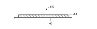
- FIG. 2 is a cross-sectional view showing an example of a circuit board in a state in which a resin laminate is formed.
- FIG. 2 is a cross-sectional view showing an example of a circuit board in which wiring is formed on a resin laminate.
- FIG. 2 is a cross-sectional view showing an example of a circuit board in which a resin laminate is further formed on the resin laminate.
- FIG. 2 is a cross-sectional view showing an example of a circuit board in which a conductive paste is applied onto wiring.
- FIG. 1 is a diagram illustrating an example of a circuit forming device.
- FIG. 2 is a block diagram showing an example of a control device.
- FIG. 2 is a cross-sectional view showing an example of a circuit board in a state in which a resin laminate is formed.
- FIG. 2 is a
- FIG. 2 is a cross-sectional view showing an example of a circuit board in a state in which a thermosetting resin is applied onto a resin laminate.
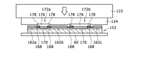
- FIG. 2 is a cross-sectional view showing an example of a circuit board on which electronic components are mounted.
- FIG. 2 is a cross-sectional view showing an example of a circuit board in a state in which an electronic component is pressed against a resin laminate.
- 1 is a cross-sectional view showing an example of a circuit board in which a thermosetting resin is applied around an electronic component.
- 1 is a cross-sectional view showing an example of a circuit board in which a resin laminate covering an upper surface and a side surface of an electronic component is formed.
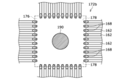
- FIG. 1 is a plan view showing an example of a circuit board on which bale-shaped dummy bumps and bumps are formed;
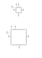
- FIG. 1 is a plan view showing an example of a circuit board on which a plurality of radial dummy bumps are formed.
- FIG. 1 is a plan view showing an example of a circuit board on which one circular dummy bump is formed.
- FIG. 1 is a plan view showing an example of a circuit board on which circular dummy bumps and bumps are formed.
- FIG. 1 shows an example of a circuit forming device 10.
- the circuit forming device 10 includes a conveying device 20, a first modeling unit 22, a second modeling unit 23, a third modeling unit 24, a fourth modeling unit 25, a pressing unit 26, a mounting unit 27, and a control device (see FIG. 2) 28.
- the conveying device 20, the first modeling unit 22, the second modeling unit 23, the third modeling unit 24, the fourth modeling unit 25, the pressing unit 26, and the mounting unit 27 are arranged on a base 29 of the circuit forming device 10.
- the base 29 is generally rectangular in shape, and in the following description, the longitudinal direction of the base 29 is referred to as the X-axis direction, the lateral direction of the base 29 as the Y-axis direction, and the direction perpendicular to both the X-axis direction and the Y-axis direction as the Z-axis direction.
- the transport device 20 includes an X-axis slide mechanism 30 and a Y-axis slide mechanism 32.
- the X-axis slide mechanism 30 includes an X-axis slide rail 34 and an X-axis slider 36.
- the X-axis slide rail 34 is disposed on the base 29 so as to extend in the X-axis direction.
- the X-axis slider 36 is held by the X-axis slide rail 34 so as to be slidable in the X-axis direction.
- the X-axis slide mechanism 30 also includes an electromagnetic motor (see FIG. 2) 38, and the X-axis slider 36 is moved to any position in the X-axis direction by the drive of the electromagnetic motor 38.
- the Y-axis slide mechanism 32 also includes a Y-axis slide rail 50 and a stage 52.
- the Y-axis slide rail 50 is disposed on the base 29 so as to extend in the Y-axis direction and is movable in the X-axis direction.
- One end of the Y-axis slide rail 50 is connected to the X-axis slider 36.
- the stage 52 is held by the Y-axis slide rail 50 so as to be slidable in the Y-axis direction.
- the Y-axis slide mechanism 32 has an electromagnetic motor (see FIG. 2) 56, and the stage 52 moves to any position in the Y-axis direction by driving the electromagnetic motor 56. As a result, the stage 52 moves to any position on the base 29 by driving the X-axis slide mechanism 30 and the Y-axis slide mechanism 32.
- the stage 52 has a base 60, a holding device 62, a lifting device (see FIG. 2) 64, and a heater (see FIG. 2) 66.
- the base 60 is formed in a flat plate shape, and a substrate is placed on the upper surface.
- the holding devices 62 are provided on both sides of the base 60 in the X-axis direction.
- the substrate is fixedly held by clamping both edges in the X-axis direction of the substrate placed on the base 60 between the holding devices 62.
- the lifting device 64 is disposed below the base 60, and raises and lowers the base 60.
- the heater 66 is built into the base 60, and heats the substrate placed on the base 60 to a desired temperature.
- the first modeling unit 22 is a unit that models the wiring of the circuit board, and has a first printing section 72 and a baking section 74.
- the first printing section 72 has an inkjet head (see FIG. 2) 76 that ejects metal ink in lines.
- the metal ink is a dispersion of nanometer-sized metal particles, such as silver particles, in a solvent. The surfaces of the metal particles are coated with a dispersant to prevent aggregation in the solvent.
- the inkjet head 76 ejects the metal ink from multiple nozzles, for example, by a piezo method using piezoelectric elements.
- the baking section 74 has an infrared irradiation device 78 (see Figure 2).
- the infrared irradiation device 78 is a device that irradiates the ejected metal ink with infrared rays.
- the metal ink irradiated with infrared rays is baked, and wiring is formed.
- baking of metal ink is a phenomenon in which, by applying energy, the solvent is evaporated and the protective film for the metal particles, i.e., the dispersant is decomposed, and the metal particles come into contact or fuse together, thereby increasing the conductivity. Then, by baking the metal ink, metal wiring is formed.
- the second modeling unit 23 is a unit that models the resin layer of the circuit board, and has a second printing unit 84 and a curing unit 86.
- the second printing unit 84 has an inkjet head (see FIG. 2) 88 that ejects ultraviolet curable resin.
- the ultraviolet curable resin is a resin that hardens when exposed to ultraviolet light.
- the inkjet head 88 may be, for example, a piezo type that uses a piezoelectric element, or a thermal type that heats the resin to generate bubbles and ejects the resin from multiple nozzles.
- the curing section 86 has a flattening device (see FIG. 2) 90 and an irradiation device (see FIG. 2) 92.
- the flattening device 90 flattens the top surface of the UV-curable resin discharged by the inkjet head 88, for example by leveling the surface of the UV-curable resin while scraping off excess resin with a roller or blade, thereby making the thickness of the UV-curable resin uniform.
- the irradiation device 92 has a mercury lamp or LED as a light source, and irradiates the discharged UV-curable resin with ultraviolet light. This hardens the discharged UV-curable resin, forming a resin layer.
- the third modeling unit 24 is a unit that models the connection parts between the electrodes of electronic components and the wiring on the circuit board, and has a third printing unit 100.
- the third printing unit 100 has a dispenser (see FIG. 2) 106 that dispenses conductive paste.
- the conductive paste is a resin that hardens when heated at a relatively low temperature, with micrometer-sized metal particles dispersed in it. Incidentally, the metal particles are in the form of flakes, and the viscosity of the conductive paste is relatively high compared to metal ink.
- the conductive paste dispensed by the dispenser 106 is then heated by the heater 66 built into the base 60.
- the resin in the heated conductive paste hardens.
- the resin in the conductive paste hardens and shrinks, and the flake-shaped metal particles dispersed in the resin come into contact with each other. This causes the conductive paste to exhibit conductivity.
- the resin in the conductive paste is an organic adhesive, and exerts adhesive power by hardening when heated.
- the fourth modeling unit 25 is a unit that models resin for fixing electronic components to a circuit board, and has a fourth printing unit 110.
- the fourth printing unit 110 has a dispenser 116 (see FIG. 2), which dispenses thermosetting resin.
- Thermosetting resin is resin that hardens when heated.
- the dispenser 116 is, for example, an air pulse type that uses compressed air.
- the thermosetting resin dispensed by the dispenser 116 is heated by a heater 66 built into the base 60 and hardens.
- the pressing unit 26 is a unit for pressing the circuit board, and has a pressing section 120.
- the pressing section 120 has a pressing plate (see FIG. 9) 122, a rubber plate (see FIG. 9) 124, and a cylinder (see FIG. 2).
- the rubber plate 124 is molded, for example, from silicon rubber and has a plate shape.
- the pressing plate 122 is molded, for example, from steel and has a plate shape.
- the rubber plate 124 is attached to the underside of the pressing plate 122, and the pressing plate 122 is pressed against the circuit board by the operation of the cylinder 126. As a result, the circuit board is pressed by the pressing plate 122 via the rubber plate 124.
- the force pressing the board can be controllably changed by controlling the operation of the cylinder 126.
- the mounting unit 27 is a unit that mounts electronic components on a circuit board, and has a supply section 130 and a mounting section 132.
- the supply section 130 has multiple tape feeders (see FIG. 2) 134 that feed taped electronic components one by one, and supplies the electronic components at a supply position.
- the supply section 130 is not limited to tape feeders 134, and may be a tray-type supply device that picks up and supplies electronic components from a tray.
- the supply section 130 may also be configured to include both tape-type and tray-type supply devices, or other types of supply devices.
- the mounting section 132 has a mounting head (see FIG. 2) 136 and a moving device (see FIG. 2) 138.
- the mounting head 136 has a suction nozzle (not shown) for suctioning and holding electronic components.
- the suction nozzle sucks and holds the electronic component by sucking air when negative pressure is supplied from a positive and negative pressure supply device (not shown).
- the positive and negative pressure supply device then supplies a slight positive pressure to release the electronic component.
- the moving device 138 also moves the mounting head 136 between the supply position of electronic components by the tape feeder 134 and the board placed on the base 60. As a result, in the mounting section 132, the electronic component supplied from the tape feeder 134 is held by the suction nozzle, and the electronic component held by the suction nozzle is mounted on the board.
- the control device 28 includes a controller 140 and a plurality of drive circuits 142.
- the plurality of drive circuits 142 are connected to the electromagnetic motors 38, 56, the holding device 62, the lifting device 64, the heater 66, the inkjet head 76, the infrared irradiation device 78, the inkjet head 88, the flattening device 90, the irradiation device 92, the dispenser 106, the dispenser 116, the cylinder 126, the tape feeder 134, the mounting head 136, and the moving device 138.
- the controller 140 includes a CPU, ROM, RAM, etc., and is mainly a computer, and is connected to the plurality of drive circuits 142. As a result, the operation of the transport device 20, the first modeling unit 22, the second modeling unit 23, the third modeling unit 24, the fourth modeling unit 25, the pressing unit 26, and the mounting unit 27 is controlled by the controller 140.
- a resin laminate is formed on the base 60 with the above-mentioned configuration, and wiring is formed on the upper surface of the resin laminate. Then, the electrodes of the electronic components are electrically connected to the wiring via the conductive paste, and the electronic components are fixed with resin to form a circuit board.
- a process for forming a circuit board will now be described. Specifically, first, the stage 52 is moved below the second modeling unit 23. Then, in the second modeling unit 23, as shown in FIG. 3, a resin laminate 152 is formed on the base 60 of the stage 52.
- the resin laminate 152 is formed by repeatedly ejecting ultraviolet curable resin from the inkjet head 88 and irradiating the ejected ultraviolet curable resin with ultraviolet light by the irradiation device 92.
- the inkjet head 88 ejects the ultraviolet curing resin in a thin film on the upper surface of the base 60.
- the ultraviolet curing resin is flattened by the flattening device 90 in the curing section 86 so that the film thickness of the ultraviolet curing resin is uniform.
- the irradiation device 92 irradiates the thin film of ultraviolet curing resin with ultraviolet light. This forms a thin film resin layer 153 on the base 60.
- the inkjet head 88 ejects a thin film of ultraviolet curable resin onto the thin film resin layer 153.
- the thin film of ultraviolet curable resin is then flattened by the flattening device 90, and the irradiation device 92 irradiates the ejected thin film of ultraviolet curable resin with ultraviolet light, thereby laminating a thin film of resin layer 153 on top of the thin film of resin layer 153.
- the ejection of ultraviolet curable resin onto the thin film of resin layer 153 and the irradiation of ultraviolet light are repeated, and multiple resin layers 153 are laminated to form a resin laminate 152.
- the stage 52 is moved below the first modeling unit 22.
- the inkjet head 76 ejects the metal ink 160 in a line shape according to the circuit pattern onto the upper surface of the resin laminate 152, as shown in FIG. 4.
- the infrared irradiation device 78 irradiates the metal ink 160 ejected according to the circuit pattern with infrared rays. As a result, the metal ink 160 is baked, and wiring 162 is formed on the upper surface of the resin laminate 152. Note that in FIG.
- wiring 162a the wiring on the left side in FIG. 4 is described as wiring 162a
- the wiring in the center is described as wiring 162b
- the wiring on the right side is described as wiring 162c.
- the inkjet head 88 ejects the ultraviolet curing resin in a thin film so that the ends of the three wirings 162 are exposed.
- the ultraviolet curing resin is flattened in the curing section 86 so that the film thickness of the ultraviolet curing resin is uniform.
- the irradiation device 92 irradiates the thin film of ultraviolet curing resin with ultraviolet light. As a result, a resin layer 156 is formed on the resin laminate 152, as shown in FIG. 5.
- the inkjet head 88 ejects the ultraviolet curing resin in a thin film only on the resin layer 156. That is, the inkjet head 88 ejects the ultraviolet curing resin in a thin film on the resin layer 156 so that the ends of the three wirings 162 are exposed.
- the thin film of ultraviolet curing resin is then flattened by the flattening device 90, and the irradiation device 92 irradiates the ultraviolet curing resin ejected in a thin film with ultraviolet light, thereby laminating the resin layer 156 on the resin layer 156.
- the ejection of the ultraviolet curing resin on the resin layer 156 and the irradiation of ultraviolet light are repeated, and a plurality of resin layers 156 are laminated to form the resin laminate 157.
- the resin laminate 157 is formed on the resin laminate 152, and the step between the resin laminate 152 and the resin laminate 157 functions as the cavity 154.
- the stage 52 is moved below the third modeling unit 24.
- the dispenser 106 dispenses conductive paste 166 onto both ends of the wiring 162b and onto the ends of the wiring 162a and wiring 162c that face both ends of the wiring 162b, as shown in FIG. 6.
- the conductive paste 166 is dispensed onto the ends of the wiring 162 in this way, the resin laminate 152 is heated by the heater 66 built into the base 60. At this time, the conductive paste 166 is heated through the resin laminate 152 and hardens. As a result, the conductive paste 166 exhibits conductivity.
- the hardened conductive paste 166 functions as a bump, so the hardened conductive paste 166 is described as a bump 168.
- the stage 52 is moved below the fourth modeling unit 25.
- the dispenser 116 dispenses the thermosetting resin 170 onto the upper surface of the resin laminate 152 between the ends of the two opposing wirings 162a, b, as shown in FIG. 7, and dispenses the thermosetting resin 170 onto the upper surface of the resin laminate 152 between the ends of the two opposing wirings 162b, c.
- thermosetting resin 170 is discharged onto the upper surface of the resin laminate 152 between the ends of the two opposing wirings 162
- the stage 52 is moved below the mounting unit 27.
- an electronic component (see FIG. 8) 172 is supplied by the tape feeder 134, and the electronic component 172 is held by the suction nozzle of the mounting head 136.
- the electronic component 172 is composed of a component body 176 and a number of electrodes 178 arranged on the lower surface of the component body 176.
- the mounting head 136 is then moved by the moving device 138, and the electronic component 172 held by the suction nozzle is mounted inside the cavity 154 of the resin laminate 152, as shown in FIG. 8.
- FIG. 8 In FIG.
- two electronic components 172 are mounted inside the cavity 154, and the two electronic components 172 are different in size.
- the small-sized electronic component is referred to as electronic component 172a
- the large-sized electronic component is referred to as electronic component 172b.
- the two electronic components 172a and 172b are mounted inside cavity 154 so that electronic component 172a is electrically connected to the two wirings 162a and 162b, and electronic component 172b is electrically connected to the two wirings 162b and 162c.
- electronic component 172a is mounted so that electrode 178 contacts bump 168 formed on wiring 162a, b.
- component body 176 of electronic component 172a contacts thermosetting resin 170 discharged between wiring 162a, b.
- Electronic component 172b is mounted so that electrode 178 contacts bump 168 formed on wiring 162b, c.
- component body 176 of electronic component 172b contacts thermosetting resin 170 discharged between wiring 162b, c.
- conductive paste 166 is discharged at the intended mounting position of electrode 178 on wiring 162
- thermosetting resin 170 is discharged at the intended mounting position of component body 176.
- thermosetting resin 170 that contacts the component body 176 is sealed between the component body 176 and the resin laminate 152. In other words, the thermosetting resin 170 is sealed between the upper surface of the resin laminate 152 and the lower surface of the component body 176.
- the stage 52 is moved below the pressing unit 26. Then, in the pressing portion 120 of the pressing unit 26, the electronic component 172 is pressed from above downward by the pressing plate 122 via the rubber plate 124, as shown in FIG. 9. Also, while the electronic component 172 is being pressed in the pressing unit 26, the resin laminate 152 is heated by the heater 66 built into the base 60. As a result, the thermosetting resin 170 is heated via the resin laminate 152 and hardens. In this manner, the electronic component 172 is pressed by the pressing plate 122, so that the component body 176 and the thermosetting resin 170 come into close contact with each other, and the electrodes 178 and the bumps 168 come into close contact with each other.
- the adhesive force of the thermosetting resin 170 fixes the electronic component 172 to the upper surface of the resin laminate 152 in the component body 176, and the adhesive force between the electrodes 178 and the bumps 168 ensures electrical connection between the electronic component 172 and the wiring 162.
- the stage 52 is moved below the fourth modeling unit 25.
- the dispenser 116 ejects the thermosetting resin 180 between the side of the component body 176 of the electronic component 172 and the cavity 154, as shown in FIG. 10.
- the resin laminate 152 is heated by the heater 66 built into the base 60.
- the thermosetting resin 180 is heated through the resin laminate 152 and hardened.
- the thermosetting resin 180 hardens while covering the side of the component body 176.
- thermosetting resins 170, 180 are sealed between the upper surface of the resin laminate 152 and the lower surface of the component body 176, and harden while covering the side of the component body 176. This fixes the electronic component 172 mounted inside the cavity 154 with the hardened resin.
- the stage 52 is moved below the second modeling unit 23.
- the inkjet head 88 ejects the ultraviolet curing resin in a thin film form so as to cover the resin laminate 157 and the electronic component 172.
- the ultraviolet curing resin is flattened in the curing section 86 so that the film thickness of the ultraviolet curing resin becomes uniform.
- the irradiation device 92 irradiates the thin film of ultraviolet curing resin with ultraviolet light. As a result, a resin layer 182 is formed on the resin laminate 157 and the electronic component 172, as shown in FIG. 11.
- the inkjet head 88 ejects the ultraviolet curing resin in a thin film on the resin layer 182. That is, the inkjet head 88 ejects the ultraviolet curing resin in a thin film on the resin layer 182 so as to cover the resin laminate 157 and the electronic component 172.
- the thin film of ultraviolet curing resin is then flattened by the flattening device 90, and the irradiation device 92 irradiates the ultraviolet curing resin ejected in a thin film with ultraviolet light, thereby laminating the resin layer 182 on the resin layer 182.
- the resin laminate 186 is formed on the resin laminate 157 and the electronic component 172, and the electronic component 172 is encapsulated inside the resin laminates 152, 157, and 186.
- the electronic component 172 is pressed downward by the pressing unit 26, so that the electrodes 178 and the bumps 168 come into close contact with each other, and electrical connection between the electronic component 172 and the wiring 162 is ensured.
- the circuit board created in this way two electronic components 172a, b of different sizes are attached, and the areas of the top surfaces of the electronic components pressed by the pressing plate 122 are different for the two different sized electronic components 172a, b. For this reason, when pressing the two different sized electronic components 172a, b, the difference in pressure applied to the bumps 168 may make it impossible to properly ensure electrical continuity between the electronic components 172a, b and the wiring 162.
- electronic components 172a and 172b are, for example, QFN (short for Quad Flat Non-leaded package)
- electronic components 172a and 172b are composed of a component body 176 whose upper and lower surfaces are square, and a plurality of electrodes 178 arranged on each of the four sides of the lower surface of component body 176, as shown in FIG. 12.
- Electronic component 172b is larger than electronic component 172a, and the area of the upper surface of electronic component 172b is larger than the area of the upper surface of electronic component 172a, so that when electronic component 172 is pressed, electronic component 172b is subjected to a larger pressure than electronic component 172a.
- the area of the upper surface of an electronic component is proportional to the square of the length of one side, but the total number of all electrodes of an electronic component is proportional to the number of electrodes on one side, so the larger the size of the electronic component, the greater the ratio of the area of the upper surface of electronic component 172 to the total area of all electrodes 178 in the electronic component. That is, the ratio of the area of the top surface of electronic component 172b to the total area of all electrodes 178 in electronic component 172b is greater than the ratio of the area of the top surface of electronic component 172a to the total area of all electrodes 178 in electronic component 172a.
- the pressure applied to one electrode of electronic component 172b when pressing large electronic component 172b is greater than the pressure applied to one electrode of electronic component 172a when pressing small electronic component 172a.
- bumps 168 are pressed with a greater force by the electrodes in electronic component 172b
- bumps 168 are pressed with a smaller force by the electrodes in electronic component 172a. Therefore, the pressure on bumps 168 in large electronic component 172b becomes too large, and bumps 168 are significantly crushed, which may cause adjacent bumps 168 to come into contact with each other and cause a short circuit.
- the pressure on the bump 168 is small, and it may not be possible to properly bond the bump 168 to the electrode, and therefore it may not be possible to properly ensure electrical continuity between the electronic component 172a and the wiring 162.
- the magnitude of the force acting on the bumps 168 is made uniform regardless of the size of the electronic component 172. That is, as shown in FIG. 13, not only the bumps 168 are formed at the intended mounting positions of the electrodes 178, but also the dummy bumps 190 are formed at the intended mounting positions of the component body 176.
- the pressure exerted when the electronic component 172 is pressed is distributed not only to the bumps 168 but also to the dummy bumps 190, so that the magnitude of the force acting on the bumps 168 is made uniform regardless of the size of the electronic component 172.
- the dummy bumps 190 having an area corresponding to the area of the upper surface of the electronic component 172 are formed at the intended mounting positions of the component body 176. That is, the dummy bumps 190 having a large area are formed on the large electronic component 172b, and the dummy bumps 190 having a small area are formed on the small electronic component 172a.
- the area of the dummy bump 190 is calculated so that the ratio of the area of the top surface of the electronic component 172 (hereinafter referred to as the "top surface area”) SJ to the total area SB of the area of the bump 168 in contact with the electrode 178 and the dummy bump 190 in contact with the component body 176 (hereinafter referred to as the "contact area”) is the same regardless of the size of the electronic component 172.
- the area of the dummy bump 190 of each of the electronic components 172a and b is calculated so that the ratio (SJa/SBa) of the top surface area SJa of the electronic component 172a to the contact area SBa of the electronic component 172a and the ratio (SJb/SBb) of the top surface area SJb of the electronic component 172b to the contact area SBb of the electronic component 172b are the same.
- the contact area SB is indicated by diagonal lines.
- the calculated area of the dummy bump 190 is divided by the area of one bump 168 to calculate the number of dummy bumps 190.
- the arrangement positions of the calculated number of dummy bumps 190 aligned at the intended mounting positions of the component body 176 are calculated. Specifically, for example, in the large electronic component 172b, when 12 dummy bumps 190 are calculated, the arrangement positions of the dummy bumps 190 aligned in a 3 ⁇ 4 array at the intended mounting positions of the component body 176 are calculated. On the other hand, for example, in the small electronic component 172a, when one dummy bump 190 is calculated, the arrangement positions of the dummy bumps 190 aligned at the center of the intended mounting positions of the component body 176 are calculated.
- the arrangement position of the aligned dummy bumps 190 is a position on one side of the component body 176 that is parallel and perpendicular to the direction in which the multiple bumps 168 are arranged.
- the arrangement positions of the dummy bumps 190 are calculated so that the shape of the dummy bumps 190 is the same as the shape of the bumps 168.
- the calculated number and positions of the dummy bumps 190 are stored in the control device 28.
- the number and positions of the bumps 168 are calculated in advance based on the number and positions of the electrodes 178 of the electronic component 172, and the calculated number and positions of the bumps 168 are also stored in the control device 28.
- the conductive paste 166 is applied to locations according to the number and positions of the bumps 168 stored in the control device 28, and the conductive paste 166 is applied to locations according to the number and positions of the dummy bumps 190 stored in the control device 28.
- the conductive paste 166 is then heated by the heater 66, whereby the bumps 168 are formed at the intended mounting positions of the electrodes 178, and the dummy bumps 190 are formed at the intended mounting positions of the component body 176.
- the thermosetting resin 170 is then applied to the intended mounting positions of the component body 176, avoiding the dummy bumps 190, and the electronic component 172 is then mounted.
- the electronic component 172 is mounted so that the electrodes 178 come into contact with the bumps 168, and the component body 176 comes into contact with the dummy bumps 190. Then, when the electronic component 172 is pressed by the pressing unit 26, the bump 168 is pressed by the electrode 178, and the bump 168 and the electrode 178 come into close contact with each other. At this time, not only the bump 168 but also the dummy bump 190 with an area corresponding to the area of the upper surface of the electronic component 172 is formed at the mounting position of the electronic component 172, so the magnitude of the force acting on the bump 168 is uniform regardless of the size of the electronic component 172. This makes it possible to uniform the force pressing the bump 168, regardless of whether the electronic component 172a is small or large, 172b, and makes it possible to properly ensure the electrical continuity between the electronic component 172 and the wiring 162.
- the height dimension of the bump 168 and the height dimension of the dummy bump 190 can be made the same. This allows the electronic component 172 mounted on the bump 168 and the dummy bump 190 to be mounted horizontally without being tilted. Furthermore, the multiple dummy bumps 190 are arranged in an aligned state. This makes it possible to apply an even load to each of the multiple dummy bumps 190 when the electronic component 172 is pressed, ensuring proper mounting of the electronic component.
- the controller 140 of the control device 28 has a base forming section 200, a wiring forming section 202, a first application section 204, a second application section 206, and an attachment section 208.
- the base forming section 200 is a functional section for forming the resin laminate 152 with ultraviolet curing resin.
- the wiring forming section 202 is a functional section for forming the wiring 162 on the resin laminate 152 with metal ink 160.
- the first application section 204 is a functional section for applying the conductive paste 166 to a location corresponding to the number and position of the bumps 168 stored in the control device 28.
- the second application section 206 is a functional section for applying the conductive paste 166 to a location corresponding to the number and position of the dummy bumps 190 stored in the control device 28.
- the mounting portion 208 is a functional portion for mounting the electronic component 172 so that the electrode 178 contacts the bump 168 and the component body 176 contacts the dummy bump 190.
- the circuit forming device 10 is an example of an electric circuit forming device.
- the third modeling unit 24 is an example of a coating device.
- the mounting unit 27 is an example of a mounting device.
- the control device 28 is an example of a control device.
- the resin laminate 152 is an example of a base.
- the wiring 162 is an example of a wiring.
- the electronic component 172 is an example of an electronic component.
- the component body 176 is an example of a component body.
- the electrode 178 is an example of an electrode.
- the process performed by the base forming unit 200 is an example of a base forming process.
- the process performed by the wiring forming unit 202 is an example of a wiring forming process.
- the process and processing performed by the first coating unit 204 are an example of a first coating process and a first coating process.
- the process and processing performed by the second coating unit 206 are an example of a second coating process and a second coating process.
- the process and processing performed by the mounting unit 208 are an example of a mounting process and a mounting process.
- 12 dummy bumps 190 are arranged in a 3 ⁇ 4 array at the intended mounting position of the component body 176.
- 12 dummy bumps 190 may be arranged radially at the intended mounting position of the component body 176.
- thermosetting resin 170 can be suitably permeated through the gaps between the dummy bumps 190 onto the underside of the component body 176.
- the shape of the dummy bump 190 is the same as the shape of the bump 168, but it may be a shape different from the shape of the bump 168.
- multiple dummy bumps 190 are formed, but it may be a single dummy bump 190. That is, as shown in FIG. 15, a single circular dummy bump 190 may be formed in the center of the intended mounting position of the component body 176.
- the bump 168 is formed not only at the intended mounting position of the electrode 178, but also protruding from the intended mounting position in the direction in which the wiring 162 extends, but as shown in FIG. 16, the bump 168 may be formed only at the intended mounting position of the electrode 178.
- the bump 168 is circular, it is preferable that the dummy bump 190 also have the same circular shape as the bump 168.
- dummy bumps 190 are also formed on the small electronic components 172a, but dummy bumps 190 do not necessarily have to be formed on the small electronic components 172a.
- a QFN in which electrodes 178 are arranged on the four sides of the underside of the component body 176 is used as the electronic component 172, but a SON (short for Small Outline Non-leaded Package) in which electrodes are arranged on two sides of the underside of the component body 176 may also be used.
- the dummy bump 190 is formed with an area corresponding to the area of the upper surface of the electronic component 172, but the dummy bump 190 may be formed with an area corresponding to the area of the lower surface of the electronic component 172. Also, the dummy bump 190 may be formed with an area corresponding to the dimensions, not the area, of the upper or lower surface of the electronic component 172. In other words, when the upper or lower surface of the electronic component 172 is square, the dummy bump 190 may be formed with an area corresponding to the length dimension of one side of the upper or lower surface of the electronic component 172.
- the dummy bump 190 may be formed with an area corresponding to the aspect ratio of the upper or lower surface of the electronic component 172. Also, the amount of dummy bump 190 may be formed according to the area of the upper or lower surface of the electronic component 172. That is, for example, the amount of dummy bump 190, i.e., the amount of conductive paste dispensed, may be adjusted so that the area of dummy bump 190 as viewed from above corresponds to the area of the upper or lower surface of electronic component 172.
- the electronic component 172 is pressed by the pressing plate 122 after being mounted, but it does not have to be pressed by the pressing plate 122. Even if the electronic component 172 is not pressed by the pressing plate 122 in this way, the electronic component 172 can be properly supported by the bumps 168 and dummy bumps 190 by placing the electronic component 172 on the bumps 168 and dummy bumps 190.
- Circuit forming device (electrical circuit forming device) 24: Third modeling unit (base forming device) 27: Mounting unit (mounting device) 28: Control device 152: Resin laminate (base) 162: Wiring 172: Electronic component 176: Component body 178: Electrode 200: Base forming section (base forming process) 202: Wiring forming section (wiring forming process) 204: First coating section (first coating process) (first coating process) 206: Second coating section (second coating process) (second coating process) 208: Mounting section (mounting process) (mounting process) (mounting process) (mounting process)
Landscapes
- Engineering & Computer Science (AREA)
- Manufacturing & Machinery (AREA)
- Microelectronics & Electronic Packaging (AREA)
- Electric Connection Of Electric Components To Printed Circuits (AREA)
Priority Applications (2)
| Application Number | Priority Date | Filing Date | Title |
|---|---|---|---|
| JP2025521727A JPWO2024241533A1 (https=) | 2023-05-24 | 2023-05-24 | |
| PCT/JP2023/019335 WO2024241533A1 (ja) | 2023-05-24 | 2023-05-24 | 電気回路形成方法、および電気回路形成装置 |
Applications Claiming Priority (1)
| Application Number | Priority Date | Filing Date | Title |
|---|---|---|---|
| PCT/JP2023/019335 WO2024241533A1 (ja) | 2023-05-24 | 2023-05-24 | 電気回路形成方法、および電気回路形成装置 |
Publications (1)
| Publication Number | Publication Date |
|---|---|
| WO2024241533A1 true WO2024241533A1 (ja) | 2024-11-28 |
Family
ID=93589860
Family Applications (1)
| Application Number | Title | Priority Date | Filing Date |
|---|---|---|---|
| PCT/JP2023/019335 Ceased WO2024241533A1 (ja) | 2023-05-24 | 2023-05-24 | 電気回路形成方法、および電気回路形成装置 |
Country Status (2)
| Country | Link |
|---|---|
| JP (1) | JPWO2024241533A1 (https=) |
| WO (1) | WO2024241533A1 (https=) |
Citations (4)
| Publication number | Priority date | Publication date | Assignee | Title |
|---|---|---|---|---|
| JPH05228415A (ja) * | 1992-02-20 | 1993-09-07 | Pfu Ltd | 接着剤塗布機構 |
| JP2007142017A (ja) * | 2005-11-16 | 2007-06-07 | Matsushita Electric Ind Co Ltd | 半導体装置およびその製造方法 |
| WO2022113186A1 (ja) * | 2020-11-25 | 2022-06-02 | 株式会社Fuji | 電気回路形成方法 |
| WO2022195800A1 (ja) * | 2021-03-18 | 2022-09-22 | 株式会社Fuji | 電子部品装着方法、および電子部品装着装置 |
-
2023
- 2023-05-24 WO PCT/JP2023/019335 patent/WO2024241533A1/ja not_active Ceased
- 2023-05-24 JP JP2025521727A patent/JPWO2024241533A1/ja active Pending
Patent Citations (4)
| Publication number | Priority date | Publication date | Assignee | Title |
|---|---|---|---|---|
| JPH05228415A (ja) * | 1992-02-20 | 1993-09-07 | Pfu Ltd | 接着剤塗布機構 |
| JP2007142017A (ja) * | 2005-11-16 | 2007-06-07 | Matsushita Electric Ind Co Ltd | 半導体装置およびその製造方法 |
| WO2022113186A1 (ja) * | 2020-11-25 | 2022-06-02 | 株式会社Fuji | 電気回路形成方法 |
| WO2022195800A1 (ja) * | 2021-03-18 | 2022-09-22 | 株式会社Fuji | 電子部品装着方法、および電子部品装着装置 |
Also Published As
| Publication number | Publication date |
|---|---|
| JPWO2024241533A1 (https=) | 2024-11-28 |
Similar Documents
| Publication | Publication Date | Title |
|---|---|---|
| JP7670731B2 (ja) | 電気回路形成方法、および電気回路形成装置 | |
| JP7316742B2 (ja) | 3次元積層造形による実装基板の製造方法 | |
| JP7624059B2 (ja) | 電子部品装着方法、および電子部品装着装置 | |
| JP6554541B2 (ja) | 配線形成方法および配線形成装置 | |
| JP7549006B2 (ja) | 回路形成方法、および回路形成装置 | |
| WO2020012626A1 (ja) | 回路形成方法、および回路形成装置 | |
| JP7238206B2 (ja) | 造形方法 | |
| JP7826344B2 (ja) | 電気回路形成方法、および電気回路形成装置 | |
| JP7282906B2 (ja) | 部品装着方法、および部品装着装置 | |
| WO2024241533A1 (ja) | 電気回路形成方法、および電気回路形成装置 | |
| US20250142734A1 (en) | Electrical circuit formation method, and electrical circuit formation device | |
| WO2024062605A1 (ja) | 回路形成装置、および回路形成方法 | |
| JP7411452B2 (ja) | 回路形成方法 | |
| JP7455953B2 (ja) | 配線形成方法 | |
| WO2024257216A1 (ja) | 回路形成方法、および回路形成装置 | |
| JP7761585B2 (ja) | 回路形成方法 | |
| JP7811218B2 (ja) | 回路形成方法、および回路形成装置 | |
| WO2023067707A1 (ja) | 3次元造形装置、およびパレット移載方法 | |
| JP7811596B2 (ja) | 電気回路形成方法、および電気回路形成装置 | |
| JP7839605B2 (ja) | 電気回路形成方法 | |
| WO2026033712A1 (ja) | 回路形成方法、および回路形成装置 | |
| JP7783298B2 (ja) | 回路形成方法、および回路形成装置 | |
| WO2024185135A1 (ja) | 電気回路形成方法、および電気回路形成装置 | |
| WO2024246986A1 (ja) | 回路形成方法、および回路形成装置 | |
| WO2025220064A1 (ja) | 回路形成方法、および回路形成装置 |
Legal Events
| Date | Code | Title | Description |
|---|---|---|---|
| 121 | Ep: the epo has been informed by wipo that ep was designated in this application |
Ref document number: 23938496 Country of ref document: EP Kind code of ref document: A1 |
|
| ENP | Entry into the national phase |
Ref document number: 2025521727 Country of ref document: JP Kind code of ref document: A |
|
| WWE | Wipo information: entry into national phase |
Ref document number: 2025521727 Country of ref document: JP |
|
| NENP | Non-entry into the national phase |
Ref country code: DE |