WO2024241134A1 - 駆動回路、表示装置及び電子機器 - Google Patents
駆動回路、表示装置及び電子機器 Download PDFInfo
- Publication number
- WO2024241134A1 WO2024241134A1 PCT/IB2024/054606 IB2024054606W WO2024241134A1 WO 2024241134 A1 WO2024241134 A1 WO 2024241134A1 IB 2024054606 W IB2024054606 W IB 2024054606W WO 2024241134 A1 WO2024241134 A1 WO 2024241134A1
- Authority
- WO
- WIPO (PCT)
- Prior art keywords
- transistor
- terminal
- electrically connected
- drain
- wiring
- Prior art date
- Legal status (The legal status is an assumption and is not a legal conclusion. Google has not performed a legal analysis and makes no representation as to the accuracy of the status listed.)
- Ceased
Links
Images




























Classifications
-
- G—PHYSICS
- G09—EDUCATION; CRYPTOGRAPHY; DISPLAY; ADVERTISING; SEALS
- G09F—DISPLAYING; ADVERTISING; SIGNS; LABELS OR NAME-PLATES; SEALS
- G09F9/00—Indicating arrangements for variable information in which the information is built-up on a support by selection or combination of individual elements
- G09F9/30—Indicating arrangements for variable information in which the information is built-up on a support by selection or combination of individual elements in which the desired character or characters are formed by combining individual elements
-
- G—PHYSICS
- G09—EDUCATION; CRYPTOGRAPHY; DISPLAY; ADVERTISING; SEALS
- G09F—DISPLAYING; ADVERTISING; SIGNS; LABELS OR NAME-PLATES; SEALS
- G09F9/00—Indicating arrangements for variable information in which the information is built-up on a support by selection or combination of individual elements
- G09F9/30—Indicating arrangements for variable information in which the information is built-up on a support by selection or combination of individual elements in which the desired character or characters are formed by combining individual elements
- G09F9/33—Indicating arrangements for variable information in which the information is built-up on a support by selection or combination of individual elements in which the desired character or characters are formed by combining individual elements being semiconductor devices, e.g. diodes
-
- G—PHYSICS
- G09—EDUCATION; CRYPTOGRAPHY; DISPLAY; ADVERTISING; SEALS
- G09G—ARRANGEMENTS OR CIRCUITS FOR CONTROL OF INDICATING DEVICES USING STATIC MEANS TO PRESENT VARIABLE INFORMATION
- G09G3/00—Control arrangements or circuits, of interest only in connection with visual indicators other than cathode-ray tubes
- G09G3/20—Control arrangements or circuits, of interest only in connection with visual indicators other than cathode-ray tubes for presentation of an assembly of a number of characters, e.g. a page, by composing the assembly by combination of individual elements arranged in a matrix no fixed position being assigned to or needed to be assigned to the individual characters or partial characters
-
- G—PHYSICS
- G09—EDUCATION; CRYPTOGRAPHY; DISPLAY; ADVERTISING; SEALS
- G09G—ARRANGEMENTS OR CIRCUITS FOR CONTROL OF INDICATING DEVICES USING STATIC MEANS TO PRESENT VARIABLE INFORMATION
- G09G3/00—Control arrangements or circuits, of interest only in connection with visual indicators other than cathode-ray tubes
- G09G3/20—Control arrangements or circuits, of interest only in connection with visual indicators other than cathode-ray tubes for presentation of an assembly of a number of characters, e.g. a page, by composing the assembly by combination of individual elements arranged in a matrix no fixed position being assigned to or needed to be assigned to the individual characters or partial characters
- G09G3/22—Control arrangements or circuits, of interest only in connection with visual indicators other than cathode-ray tubes for presentation of an assembly of a number of characters, e.g. a page, by composing the assembly by combination of individual elements arranged in a matrix no fixed position being assigned to or needed to be assigned to the individual characters or partial characters using controlled light sources
- G09G3/30—Control arrangements or circuits, of interest only in connection with visual indicators other than cathode-ray tubes for presentation of an assembly of a number of characters, e.g. a page, by composing the assembly by combination of individual elements arranged in a matrix no fixed position being assigned to or needed to be assigned to the individual characters or partial characters using controlled light sources using electroluminescent panels
- G09G3/32—Control arrangements or circuits, of interest only in connection with visual indicators other than cathode-ray tubes for presentation of an assembly of a number of characters, e.g. a page, by composing the assembly by combination of individual elements arranged in a matrix no fixed position being assigned to or needed to be assigned to the individual characters or partial characters using controlled light sources using electroluminescent panels semiconductive, e.g. using light-emitting diodes [LED]
-
- G—PHYSICS
- G09—EDUCATION; CRYPTOGRAPHY; DISPLAY; ADVERTISING; SEALS
- G09G—ARRANGEMENTS OR CIRCUITS FOR CONTROL OF INDICATING DEVICES USING STATIC MEANS TO PRESENT VARIABLE INFORMATION
- G09G3/00—Control arrangements or circuits, of interest only in connection with visual indicators other than cathode-ray tubes
- G09G3/20—Control arrangements or circuits, of interest only in connection with visual indicators other than cathode-ray tubes for presentation of an assembly of a number of characters, e.g. a page, by composing the assembly by combination of individual elements arranged in a matrix no fixed position being assigned to or needed to be assigned to the individual characters or partial characters
- G09G3/22—Control arrangements or circuits, of interest only in connection with visual indicators other than cathode-ray tubes for presentation of an assembly of a number of characters, e.g. a page, by composing the assembly by combination of individual elements arranged in a matrix no fixed position being assigned to or needed to be assigned to the individual characters or partial characters using controlled light sources
- G09G3/30—Control arrangements or circuits, of interest only in connection with visual indicators other than cathode-ray tubes for presentation of an assembly of a number of characters, e.g. a page, by composing the assembly by combination of individual elements arranged in a matrix no fixed position being assigned to or needed to be assigned to the individual characters or partial characters using controlled light sources using electroluminescent panels
- G09G3/32—Control arrangements or circuits, of interest only in connection with visual indicators other than cathode-ray tubes for presentation of an assembly of a number of characters, e.g. a page, by composing the assembly by combination of individual elements arranged in a matrix no fixed position being assigned to or needed to be assigned to the individual characters or partial characters using controlled light sources using electroluminescent panels semiconductive, e.g. using light-emitting diodes [LED]
- G09G3/3208—Control arrangements or circuits, of interest only in connection with visual indicators other than cathode-ray tubes for presentation of an assembly of a number of characters, e.g. a page, by composing the assembly by combination of individual elements arranged in a matrix no fixed position being assigned to or needed to be assigned to the individual characters or partial characters using controlled light sources using electroluminescent panels semiconductive, e.g. using light-emitting diodes [LED] organic, e.g. using organic light-emitting diodes [OLED]
- G09G3/3266—Details of drivers for scan electrodes
-
- G—PHYSICS
- G09—EDUCATION; CRYPTOGRAPHY; DISPLAY; ADVERTISING; SEALS
- G09G—ARRANGEMENTS OR CIRCUITS FOR CONTROL OF INDICATING DEVICES USING STATIC MEANS TO PRESENT VARIABLE INFORMATION
- G09G3/00—Control arrangements or circuits, of interest only in connection with visual indicators other than cathode-ray tubes
- G09G3/20—Control arrangements or circuits, of interest only in connection with visual indicators other than cathode-ray tubes for presentation of an assembly of a number of characters, e.g. a page, by composing the assembly by combination of individual elements arranged in a matrix no fixed position being assigned to or needed to be assigned to the individual characters or partial characters
- G09G3/22—Control arrangements or circuits, of interest only in connection with visual indicators other than cathode-ray tubes for presentation of an assembly of a number of characters, e.g. a page, by composing the assembly by combination of individual elements arranged in a matrix no fixed position being assigned to or needed to be assigned to the individual characters or partial characters using controlled light sources
- G09G3/30—Control arrangements or circuits, of interest only in connection with visual indicators other than cathode-ray tubes for presentation of an assembly of a number of characters, e.g. a page, by composing the assembly by combination of individual elements arranged in a matrix no fixed position being assigned to or needed to be assigned to the individual characters or partial characters using controlled light sources using electroluminescent panels
- G09G3/32—Control arrangements or circuits, of interest only in connection with visual indicators other than cathode-ray tubes for presentation of an assembly of a number of characters, e.g. a page, by composing the assembly by combination of individual elements arranged in a matrix no fixed position being assigned to or needed to be assigned to the individual characters or partial characters using controlled light sources using electroluminescent panels semiconductive, e.g. using light-emitting diodes [LED]
- G09G3/3208—Control arrangements or circuits, of interest only in connection with visual indicators other than cathode-ray tubes for presentation of an assembly of a number of characters, e.g. a page, by composing the assembly by combination of individual elements arranged in a matrix no fixed position being assigned to or needed to be assigned to the individual characters or partial characters using controlled light sources using electroluminescent panels semiconductive, e.g. using light-emitting diodes [LED] organic, e.g. using organic light-emitting diodes [OLED]
- G09G3/3275—Details of drivers for data electrodes
-
- H—ELECTRICITY
- H10—SEMICONDUCTOR DEVICES; ELECTRIC SOLID-STATE DEVICES NOT OTHERWISE PROVIDED FOR
- H10B—ELECTRONIC MEMORY DEVICES
- H10B12/00—Dynamic random access memory [DRAM] devices
-
- H—ELECTRICITY
- H10—SEMICONDUCTOR DEVICES; ELECTRIC SOLID-STATE DEVICES NOT OTHERWISE PROVIDED FOR
- H10B—ELECTRONIC MEMORY DEVICES
- H10B41/00—Electrically erasable-and-programmable ROM [EEPROM] devices comprising floating gates
- H10B41/70—Electrically erasable-and-programmable ROM [EEPROM] devices comprising floating gates the floating gate being an electrode shared by two or more components
-
- H—ELECTRICITY
- H10—SEMICONDUCTOR DEVICES; ELECTRIC SOLID-STATE DEVICES NOT OTHERWISE PROVIDED FOR
- H10D—INORGANIC ELECTRIC SEMICONDUCTOR DEVICES
- H10D30/00—Field-effect transistors [FET]
- H10D30/01—Manufacture or treatment
- H10D30/021—Manufacture or treatment of FETs having insulated gates [IGFET]
-
- H—ELECTRICITY
- H10—SEMICONDUCTOR DEVICES; ELECTRIC SOLID-STATE DEVICES NOT OTHERWISE PROVIDED FOR
- H10D—INORGANIC ELECTRIC SEMICONDUCTOR DEVICES
- H10D30/00—Field-effect transistors [FET]
- H10D30/60—Insulated-gate field-effect transistors [IGFET]
- H10D30/67—Thin-film transistors [TFT]
Definitions
- One aspect of the present invention relates to a drive circuit, a display device, and an electronic device.
- one aspect of the present invention is not limited to the above technical field.
- the technical field of the invention disclosed in this specification relates to an object, an operating method, or a manufacturing method.
- one aspect of the present invention relates to a process, a machine, a manufacture, or a composition of matter. Therefore, more specifically, examples of the technical field of one aspect of the present invention disclosed in this specification include semiconductor devices, display devices (including liquid crystal display devices), light-emitting devices, power storage devices, imaging devices, memory devices, signal processing devices, sensors, processing devices (including processors), electronic devices, systems, their operating methods, their manufacturing methods, and their inspection methods.
- display devices included in wearable devices, monitors, mobile phones (e.g., smartphones), wristwatch-type information terminals, tablet-type information terminals, notebook PCs (personal computers), etc. for XR (Extended Reality or Cross Reality) such as VR (Virtual Reality) and AR (Augmented Reality).
- XR Extended Reality or Cross Reality
- VR Virtual Reality
- AR Advanced Reality
- display devices are being developed to improve screen resolution, color reproducibility (NTSC ratio), size of driving circuits, and power consumption.
- light-emitting devices having micro LEDs Light Emitting Diodes
- have attracted attention because of their long life, fast response speed, and low power consumption compared to light-emitting devices using organic EL materials.
- oxide semiconductors not only are there oxides of single-component metals such as indium oxide and zinc oxide, but also oxides of multi-component metals.
- oxides of multi-component metals in particular, research on In-Ga-Zn oxide (hereinafter also referred to as IGZO) has been actively conducted.
- Non-Patent Document 1 By using In-Ga-Zn oxide as the active layer to fabricate an n-channel transistor, the off-current of the transistor can be made extremely low (see Non-Patent Document 1).
- Non-Patent Documents 2 and 3 report on LSI (Large Scale Integration) and display devices that utilize this characteristic.
- Patent Document 1 discloses an invention for a driver circuit that includes a shift register of a unipolar circuit using n-channel transistors with an oxide semiconductor as an active layer.
- the current and brightness are proportional, so the brightness can be increased by increasing the amount of current.
- a display device that has a light-emitting device that contains organic EL materials can control the gradation of an image displayed on the display device by increasing or decreasing the amount of current.
- the brightness can also be increased by increasing the amount of current, but at the same time, wavelength shifts are more likely to occur, and the color emitted by the light-emitting device may change. For this reason, in display devices that have light-emitting devices that contain micro LEDs, a method of controlling the gradation of an image displayed on the display device by pulse width modulation (PWM) drive may be used.
- PWM pulse width modulation
- PWM driving is a driving method in which, for example, when displaying one frame of an image on a display device, a period in which a constant current flows between the anode and cathode of a light-emitting device including a micro LED and a period in which a constant current does not flow are set within that frame. In this way, by determining the time allocation between the period in which a constant current flows to the light-emitting device and the period in which a constant current does not flow within one frame, it is possible to determine the gradation of the image displayed on the display device.
- the drive circuitry of the display device when allocating time within one frame between periods when current flows and periods when current does not flow, the drive circuitry of the display device must be driven on a subframe basis. In particular, as the frame frequency increases, the time per frame becomes shorter, and control must be performed on a finer subframe basis. In other words, the drive circuitry of the display device must be capable of operating at a drive frequency higher than the desired frame frequency.
- One aspect of the present invention has an object to provide a driver circuit capable of high-speed driving. Another aspect of the present invention has an object to provide a driver circuit capable of stabilizing an output signal. Another aspect of the present invention has an object to provide a driver circuit with a reduced circuit area. Another aspect of the present invention has an object to provide a driver circuit with reduced operational defects. Another aspect of the present invention has an object to provide a display device having the driver circuit. Another aspect of the present invention has an object to provide an electronic device having the display device. Another aspect of the present invention has an object to provide a new driver circuit, a new display device, or a new electronic device.
- the problem of one embodiment of the present invention is not limited to the problem described above.
- the problem described above does not preclude the existence of other problems.
- the other problems are problems not mentioned in this section, which will be described below. Problems not mentioned in this section can be derived by a person skilled in the art from the description in the specification or drawings, etc., and can be appropriately extracted from these descriptions.
- one embodiment of the present invention solves at least one of the problems described above and other problems. Note that one embodiment of the present invention does not need to solve all of the problems described above and other problems.
- a vertical channel transistor is used in the driver circuit of one embodiment of the present invention.
- a vertical channel transistor has a structure in which the source electrode and the drain electrode are located at different heights and the current flowing through the semiconductor layer flows in the height direction, and the channel length can be made shorter than that of a planar transistor. For this reason, a vertical channel transistor can have a large on-current and a high driving frequency.
- a vertical channel transistor can be easily formed.
- One aspect of the present invention is a driver circuit including a shift register, a first holding circuit, and a second holding circuit.
- the shift register includes a first output terminal
- the first holding circuit includes a first input terminal, a second input terminal, a third input terminal, a second output terminal, and a third output terminal
- the second holding circuit includes a fourth input terminal, a fifth input terminal, a sixth input terminal, a seventh input terminal, and a fourth output terminal.
- the second output terminal is electrically connected to the fourth input terminal
- the third output terminal is electrically connected to the fifth input terminal.
- the shift register has a function of transmitting a first pulse signal to the first output terminal.
- the first holding circuit has a function of holding a first potential corresponding to the first image signal by inputting the first pulse signal to the second input terminal and the first image signal transmitted to the first wiring to the first input terminal, a function of outputting a second image signal of the same logic as the first image signal to the second output terminal, and a function of outputting a third image signal having the inverted logic of the first image signal to the third output terminal by inputting the second pulse signal transmitted to the second wiring to the third input terminal.
- the second holding circuit has a function of acquiring a second image signal input to the fourth input terminal by inputting the second pulse signal sent to the second wiring to the sixth input terminal, and holding a second potential corresponding to the second image signal, a function of acquiring a third image signal input to the fifth input terminal by inputting the second pulse signal sent to the second wiring to the seventh input terminal, and holding a third potential corresponding to the third image signal, and a function of outputting a fourth image signal having the same logic as the third image signal to the fourth output terminal using the second potential and the third potential.
- the first holding circuit may include a first transistor, a second transistor, a third transistor, and a first capacitor.
- each of the first to third transistors preferably includes a first oxide semiconductor in a channel formation region.
- the first input terminal is electrically connected to the first wiring
- the third input terminal is electrically connected to the second wiring.
- one of the source and drain of the first transistor is electrically connected to the first input terminal
- the gate of the first transistor is electrically connected to the second input terminal
- the other of the source and drain of the first transistor is electrically connected to the gate of the third transistor, the first terminal of the first capacitance element, and the second output terminal.
- one of the source and drain of the second transistor is electrically connected to the gate of the second transistor and the third input terminal
- the other of the source and drain of the second transistor is electrically connected to one of the source and drain of the third transistor and the third output terminal.
- the second holding circuit may include a fourth transistor, a fifth transistor, a sixth transistor, a seventh transistor, an eighth transistor, a ninth transistor, a second capacitor, and a third capacitor.
- each of the fourth to ninth transistors preferably includes a second oxide semiconductor in a channel formation region.
- the sixth input terminal is electrically connected to the second wiring
- the seventh input terminal is electrically connected to the second wiring.
- one of the source and drain of the fourth transistor is electrically connected to the fifth input terminal
- the gate of the fourth transistor is electrically connected to the seventh input terminal
- the other of the source and drain of the fourth transistor is electrically connected to one of the source and drain of the fifth transistor.
- the other of the source and drain of the fifth transistor is electrically connected to the gate of the sixth transistor and the first terminal of the second capacitance element.
- one of the source and drain of the sixth transistor is electrically connected to one of the source and drain of the seventh transistor, the second terminal of the second capacitance element, and the fourth output terminal.
- one of the source and drain of the eighth transistor is electrically connected to the fourth input terminal, the gate of the eighth transistor is electrically connected to the sixth input terminal, and the other of the source and drain of the eighth transistor is electrically connected to one of the source and drain of the ninth transistor, the gate of the seventh transistor, and the first terminal of the third capacitance element.
- the second holding circuit may include a fifth transistor, a sixth transistor, a seventh transistor, an eighth transistor, a ninth transistor, a second capacitor, and a third capacitor.
- each of the fifth to ninth transistors preferably includes a second oxide semiconductor in a channel formation region.
- the sixth input terminal is electrically connected to the second wiring
- the seventh input terminal is electrically connected to the second wiring.
- one of the source and drain of the fifth transistor is electrically connected to the fifth input terminal
- the gate of the fifth transistor is electrically connected to the seventh input terminal
- the other of the source and drain of the fifth transistor is electrically connected to the gate of the sixth transistor and the first terminal of the second capacitance element.
- one of the source and drain of the sixth transistor is electrically connected to one of the source and drain of the seventh transistor, the second terminal of the second capacitance element, and the fourth output terminal.
- one of the source and drain of the eighth transistor is electrically connected to the fourth input terminal, the gate of the eighth transistor is electrically connected to the sixth input terminal, and the other of the source and drain of the eighth transistor is electrically connected to one of the source and drain of the ninth transistor, the gate of the seventh transistor, and the first terminal of the third capacitance element.
- the second holding circuit may include a fourth transistor, a fifth transistor, a sixth transistor, a seventh transistor, an eighth transistor, a ninth transistor, a tenth transistor, a second capacitor, and a third capacitor.
- each of the fourth to tenth transistors preferably includes a second oxide semiconductor in a channel formation region.
- the sixth input terminal is electrically connected to the second wiring
- the seventh input terminal is electrically connected to the second wiring.
- one of the source and drain of the fourth transistor is electrically connected to the fifth input terminal
- the gate of the fourth transistor is electrically connected to the seventh input terminal
- the other of the source and drain of the fourth transistor is electrically connected to one of the source and drain of the fifth transistor and one of the source and drain of the tenth transistor.
- the other of the source and drain of the fifth transistor is electrically connected to the gate of the sixth transistor and the first terminal of the second capacitance element.
- one of the source and drain of the sixth transistor is electrically connected to one of the source and drain of the seventh transistor, the second terminal of the second capacitance element, and the fourth output terminal.
- one of the source and drain of the eighth transistor is electrically connected to the fourth input terminal
- the gate of the eighth transistor is electrically connected to the sixth input terminal
- the other of the source and drain of the eighth transistor is electrically connected to one of the source and drain of the ninth transistor, the gate of the seventh transistor, the gate of the tenth transistor, and the first terminal of the third capacitance element.
- each of the first oxide semiconductor and the second oxide semiconductor may have one or more elements selected from indium, zinc, and an element M in a channel formation region.
- the element M is one or more selected from aluminum, gallium, silicon, yttrium, tin, copper, vanadium, beryllium, boron, titanium, iron, nickel, germanium, zirconium, molybdenum, lanthanum, cerium, neodymium, hafnium, tantalum, tungsten, cobalt, magnesium, and antimony.
- Another embodiment of the present invention is a display device including the drive circuit described in (6) above and a pixel circuit, wherein the pixel circuit has a light-emitting device including an LED chip, and the pixel circuit controls whether the light-emitting device emits light or not in response to a fourth image signal output from the drive circuit.
- Another embodiment of the present invention is an electronic device including the display device described in (7) above and a housing.
- one embodiment of the present invention is a driver circuit different from the driver circuit of (1) above, which includes a shift register, a first holding circuit, and a second holding circuit.
- the shift register has a first output terminal
- the first holding circuit has a first input terminal, a second input terminal, a third input terminal, a second output terminal, and a third output terminal
- the second holding circuit has a fourth input terminal, a fifth input terminal, a sixth input terminal, and a fourth output terminal.
- the second output terminal is electrically connected to the fourth input terminal
- the third output terminal is electrically connected to the fifth input terminal.
- the shift register has a function of transmitting a first pulse signal to the first output terminal.
- the first holding circuit has a function of holding a first potential corresponding to the first image signal by inputting the first pulse signal to the second input terminal and the first image signal transmitted to the first wiring to the first input terminal, a function of outputting a second image signal having the same logic as the first image signal to the second output terminal, and a function of outputting a third image signal having the inverted logic of the first image signal to the third output terminal by inputting the second pulse signal transmitted to the second wiring to the third input terminal.
- the second holding circuit has a function of acquiring the second image signal input to the fourth input terminal by inputting the second pulse signal transmitted to the second wiring to the sixth input terminal, and holding a second potential corresponding to the second image signal, and a function of outputting a fourth image signal having the same logic as the third image signal to the fourth output terminal using the second potential and the third potential corresponding to the third image signal.
- the first holding circuit may include a first transistor, a second transistor, a third transistor, and a first capacitor.
- each of the first to third transistors preferably includes a first oxide semiconductor in a channel formation region.
- the first input terminal is electrically connected to the first wiring
- the third input terminal is electrically connected to the second wiring.
- one of the source and drain of the first transistor is electrically connected to the first input terminal
- the gate of the first transistor is electrically connected to the second input terminal
- the other of the source and drain of the first transistor is electrically connected to the gate of the third transistor, the first terminal of the first capacitance element, and the second output terminal.
- one of the source and drain of the second transistor is electrically connected to the gate of the second transistor and the third input terminal
- the other of the source and drain of the second transistor is electrically connected to one of the source and drain of the third transistor and the third output terminal.
- the second holding circuit may include a fifth transistor, a sixth transistor, a seventh transistor, an eighth transistor, a ninth transistor, a tenth transistor, a second capacitor, and a third capacitor.
- each of the fifth to tenth transistors preferably includes a second oxide semiconductor in a channel formation region.
- the sixth input terminal is preferably electrically connected to the second wiring.
- the gate of the fifth transistor is preferably electrically connected to the fifth input terminal, and one of the source and drain of the fifth transistor is preferably electrically connected to the gate of the sixth transistor, one of the source and drain of the tenth transistor, and the first terminal of the second capacitance element.
- the source and drain of the sixth transistor is preferably electrically connected to one of the source and drain of the seventh transistor, the second terminal of the second capacitance element, and the fourth output terminal.
- the source and drain of the eighth transistor is preferably electrically connected to the fourth input terminal, the gate of the eighth transistor is preferably electrically connected to the sixth input terminal, and the other of the source and drain of the eighth transistor is preferably electrically connected to one of the source and drain of the ninth transistor, the gate of the seventh transistor, the gate of the tenth transistor, and the first terminal of the third capacitance element.
- the second holding circuit may include a fifth transistor, a sixth transistor, a seventh transistor, an eighth transistor, a ninth transistor, a tenth transistor, a second capacitor, and a third capacitor, and may have a structure different from that of the above-mentioned (5).
- each of the fifth to tenth transistors preferably includes a second oxide semiconductor in a channel formation region.
- the sixth input terminal is preferably electrically connected to the second wiring
- the seventh input terminal is preferably electrically connected to the second wiring.
- one of the source and drain of the fifth transistor is electrically connected to the gate of the fifth transistor and the fifth input terminal
- the other of the source and drain of the fifth transistor is electrically connected to the gate of the sixth transistor, one of the source and drain of the tenth transistor, and the first terminal of the second capacitance element.
- one of the source and drain of the sixth transistor is electrically connected to one of the source and drain of the seventh transistor, the second terminal of the second capacitance element, and the fourth output terminal.
- one of the source and drain of the eighth transistor is electrically connected to the fourth input terminal, the gate of the eighth transistor is electrically connected to the sixth input terminal, and the other of the source and drain of the eighth transistor is electrically connected to one of the source and drain of the ninth transistor, the gate of the seventh transistor, the gate of the tenth transistor, and the first terminal of the third capacitance element.
- each of the first oxide semiconductor and the second oxide semiconductor may include one or more elements selected from indium, zinc, and an element M in a channel formation region.
- the element M is one or more selected from aluminum, gallium, silicon, yttrium, tin, copper, vanadium, beryllium, boron, titanium, iron, nickel, germanium, zirconium, molybdenum, lanthanum, cerium, neodymium, hafnium, tantalum, tungsten, cobalt, magnesium, and antimony.
- Another embodiment of the present invention is a display device including the driver circuit described in (13) above and a pixel circuit, wherein the pixel circuit has a light-emitting device including an LED chip, and the pixel circuit controls whether the light-emitting device emits light or not in response to a fourth image signal output from the driver circuit.
- Another embodiment of the present invention is an electronic device including the display device described in (14) above and a housing.
- one aspect of the present invention is a driver circuit different from the above (1) and (9), which includes a shift register, a first holding circuit, and a second holding circuit.
- the shift register has a first output terminal
- the first holding circuit has a first input terminal, a second input terminal, a third input terminal, a second output terminal, and a third output terminal
- the second holding circuit has a fourth input terminal, a fifth input terminal, a sixth input terminal, a seventh input terminal, and a fourth output terminal.
- the second output terminal is electrically connected to the fourth input terminal
- the third output terminal is electrically connected to the fifth input terminal.
- the shift register has a function of transmitting a first pulse signal to the first output terminal.
- the first holding circuit has a function of holding a first potential corresponding to the first image signal by inputting the first pulse signal to the second input terminal and the first image signal transmitted to the first wiring to the first input terminal, a function of outputting a second image signal of the same logic as the first image signal to the second output terminal, and a function of outputting a third image signal having the inverted logic of the first image signal to the third output terminal by inputting the second pulse signal transmitted to the second wiring to the third input terminal.
- the second holding circuit has a function of acquiring a second image signal input to the fourth input terminal by inputting the second pulse signal sent to the second wiring to the sixth input terminal, and holding a second potential corresponding to the second image signal, a function of acquiring a third image signal input to the fifth input terminal by inputting the second pulse signal sent to the second wiring to the seventh input terminal, and holding a third potential corresponding to the third image signal, and a function of outputting a fourth image signal having the same logic as the third image signal to the fourth output terminal using the second potential and the third potential.
- the first holding circuit and the second holding circuit each have a vertical channel transistor.
- the first holding circuit may include a first transistor, a second transistor, a third transistor, and a first capacitor, wherein each of the first transistor to the third transistor is a vertical channel transistor.
- the first input terminal is electrically connected to the first wiring
- the third input terminal is electrically connected to the second wiring.
- one of the source and drain of the first transistor is electrically connected to the first input terminal
- the gate of the first transistor is electrically connected to the second input terminal
- the other of the source and drain of the first transistor is electrically connected to the gate of the third transistor, the first terminal of the first capacitance element, and the second output terminal.
- one of the source and drain of the second transistor is electrically connected to the gate of the second transistor and the third input terminal
- the other of the source and drain of the second transistor is electrically connected to one of the source and drain of the third transistor and the third output terminal.
- the second holding circuit may include a fourth transistor, a fifth transistor, a sixth transistor, a seventh transistor, an eighth transistor, a ninth transistor, a second capacitor, and a third capacitor, wherein each of the fourth to ninth transistors is a vertical channel transistor.
- the sixth input terminal is electrically connected to the second wiring
- the seventh input terminal is electrically connected to the second wiring.
- one of the source and drain of the fourth transistor is electrically connected to the fifth input terminal
- the gate of the fourth transistor is electrically connected to the seventh input terminal
- the other of the source and drain of the fourth transistor is electrically connected to one of the source and drain of the fifth transistor.
- the other of the source and drain of the fifth transistor is electrically connected to the gate of the sixth transistor and the first terminal of the second capacitance element.
- one of the source and drain of the sixth transistor is electrically connected to one of the source and drain of the seventh transistor, the second terminal of the second capacitance element, and the fourth output terminal.
- one of the source and drain of the eighth transistor is electrically connected to the fourth input terminal, the gate of the eighth transistor is electrically connected to the sixth input terminal, and the other of the source and drain of the eighth transistor is electrically connected to one of the source and drain of the ninth transistor, the gate of the seventh transistor, and the first terminal of the third capacitance element.
- the second holding circuit may include a fifth transistor, a sixth transistor, a seventh transistor, an eighth transistor, a ninth transistor, a second capacitor, and a third capacitor, wherein each of the fifth to ninth transistors is a vertical channel transistor.
- the sixth input terminal is electrically connected to the second wiring
- the seventh input terminal is electrically connected to the second wiring.
- one of the source and drain of the fifth transistor is electrically connected to the fifth input terminal
- the gate of the fifth transistor is electrically connected to the seventh input terminal
- the other of the source and drain of the fifth transistor is electrically connected to the gate of the sixth transistor and the first terminal of the second capacitance element.
- one of the source and drain of the sixth transistor is electrically connected to one of the source and drain of the seventh transistor, the second terminal of the second capacitance element, and the fourth output terminal.
- one of the source and drain of the eighth transistor is electrically connected to the fourth input terminal, the gate of the eighth transistor is electrically connected to the sixth input terminal, and the other of the source and drain of the eighth transistor is electrically connected to one of the source and drain of the ninth transistor, the gate of the seventh transistor, and the first terminal of the third capacitance element.
- the second holding circuit may include a fourth transistor, a fifth transistor, a sixth transistor, a seventh transistor, an eighth transistor, a ninth transistor, a tenth transistor, a second capacitor, and a third capacitor, wherein each of the fourth to tenth transistors is a vertical channel transistor.
- the sixth input terminal is electrically connected to the second wiring
- the seventh input terminal is electrically connected to the second wiring.
- one of the source and drain of the fourth transistor is electrically connected to the fifth input terminal
- the gate of the fourth transistor is electrically connected to the seventh input terminal
- the other of the source and drain of the fourth transistor is electrically connected to one of the source and drain of the fifth transistor and one of the source and drain of the tenth transistor.
- the other of the source and drain of the fifth transistor is electrically connected to the gate of the sixth transistor and the first terminal of the second capacitance element.
- one of the source and drain of the sixth transistor is electrically connected to one of the source and drain of the seventh transistor, the second terminal of the second capacitance element, and the fourth output terminal.
- one of the source and drain of the eighth transistor is electrically connected to the fourth input terminal
- the gate of the eighth transistor is electrically connected to the sixth input terminal
- the other of the source and drain of the eighth transistor is electrically connected to one of the source and drain of the ninth transistor, the gate of the seventh transistor, the gate of the tenth transistor, and the first terminal of the third capacitance element.
- the vertical channel transistor may have a structure including: a first conductive layer located below the first insulating layer and functioning as one of a source and a drain; a second conductive layer located above the first insulating layer and functioning as the other of the source and drain; a semiconductor layer in contact with a side surface of an opening formed in the first insulating layer and in contact with the first conductive layer and the second conductive layer; a gate insulating film located on the semiconductor layer; and a gate electrode located on the gate insulating film.
- the thickness of the first insulating layer is preferably 50 nm to 150 nm.
- the semiconductor layer may have a channel formation region containing one or more elements selected from indium, zinc, and an element M.
- the element M is one or more selected from aluminum, gallium, silicon, yttrium, tin, copper, vanadium, beryllium, boron, titanium, iron, nickel, germanium, zirconium, molybdenum, lanthanum, cerium, neodymium, hafnium, tantalum, tungsten, cobalt, magnesium, and antimony.
- Another embodiment of the present invention is a display device including the driver circuit described in (22) above and a pixel circuit, wherein the pixel circuit has a light-emitting device including an LED chip, and the pixel circuit controls whether the light-emitting device emits light or not in response to a fourth image signal output from the driver circuit.
- Another embodiment of the present invention is an electronic device including the display device described in (23) above and a housing.
- one aspect of the present invention is a driver circuit different from the above (1), (9) and (16), which includes a shift register, a first holding circuit and a second holding circuit.
- the shift register has a first output terminal
- the first holding circuit has a first input terminal, a second input terminal, a third input terminal, a second output terminal and a third output terminal
- the second holding circuit has a fourth input terminal, a fifth input terminal, a sixth input terminal and a fourth output terminal.
- the second output terminal is electrically connected to the fourth input terminal
- the third output terminal is electrically connected to the fifth input terminal.
- the shift register has a function of transmitting a first pulse signal to the first output terminal.
- the first holding circuit has a function of holding a first potential corresponding to the first image signal by inputting the first pulse signal to the second input terminal and the first image signal transmitted to the first wiring to the first input terminal, a function of outputting a second image signal having the same logic as the first image signal to the second output terminal, and a function of outputting a third image signal having the inverted logic of the first image signal to the third output terminal by inputting the second pulse signal transmitted to the second wiring to the third input terminal.
- the second holding circuit has a function of acquiring the second image signal input to the fourth input terminal by inputting the second pulse signal transmitted to the second wiring to the sixth input terminal, and holding a second potential corresponding to the second image signal, and a function of outputting a fourth image signal having the same logic as the third image signal to the fourth output terminal using the second potential and the third potential corresponding to the third image signal.
- the first holding circuit and the second holding circuit each have a vertical channel transistor.
- the first holding circuit may include a first transistor, a second transistor, a third transistor, and a first capacitor, wherein each of the first transistor to the third transistor is a vertical channel transistor.
- the first input terminal is electrically connected to the first wiring
- the third input terminal is electrically connected to the second wiring.
- one of the source and drain of the first transistor is electrically connected to the first input terminal
- the gate of the first transistor is electrically connected to the second input terminal
- the other of the source and drain of the first transistor is electrically connected to the gate of the third transistor, the first terminal of the first capacitance element, and the second output terminal.
- one of the source and drain of the second transistor is electrically connected to the gate of the second transistor and the third input terminal
- the other of the source and drain of the second transistor is electrically connected to one of the source and drain of the third transistor and the third output terminal.
- the second holding circuit may include a fifth transistor, a sixth transistor, a seventh transistor, an eighth transistor, a ninth transistor, a tenth transistor, a second capacitor, and a third capacitor, wherein each of the fifth to tenth transistors is a vertical channel transistor.
- the sixth input terminal is preferably electrically connected to the second wiring, and the seventh input terminal is preferably electrically connected to the second wiring.
- the gate of the fifth transistor is preferably electrically connected to the fifth input terminal, and one of the source and drain of the fifth transistor is preferably electrically connected to the gate of the sixth transistor, one of the source and drain of the tenth transistor, and the first terminal of the second capacitance element.
- the source and drain of the sixth transistor is preferably electrically connected to one of the source and drain of the seventh transistor, the second terminal of the second capacitance element, and the fourth output terminal.
- the source and drain of the eighth transistor is preferably electrically connected to the fourth input terminal, the gate of the eighth transistor is preferably electrically connected to the sixth input terminal, and the other of the source and drain of the eighth transistor is preferably electrically connected to one of the source and drain of the ninth transistor, the gate of the seventh transistor, the gate of the tenth transistor, and the first terminal of the third capacitance element.
- the second holding circuit may include a fifth transistor, a sixth transistor, a seventh transistor, an eighth transistor, a ninth transistor, a tenth transistor, a second capacitor, and a third capacitor, and may have a configuration different from that of the above (15).
- each of the fifth to tenth transistors is a vertical channel transistor.
- the sixth input terminal is preferably electrically connected to the second wiring
- the seventh input terminal is preferably electrically connected to the second wiring.
- one of the source and drain of the fifth transistor is electrically connected to the gate of the fifth transistor and the fifth input terminal
- the other of the source and drain of the fifth transistor is electrically connected to the gate of the sixth transistor, one of the source and drain of the tenth transistor, and the first terminal of the second capacitance element.
- one of the source and drain of the sixth transistor is electrically connected to one of the source and drain of the seventh transistor, the second terminal of the second capacitance element, and the fourth output terminal.
- one of the source and drain of the eighth transistor is electrically connected to the fourth input terminal, the gate of the eighth transistor is electrically connected to the sixth input terminal, and the other of the source and drain of the eighth transistor is electrically connected to one of the source and drain of the ninth transistor, the gate of the seventh transistor, the gate of the tenth transistor, and the first terminal of the third capacitance element.
- the vertical channel transistor may have a structure including: a first conductive layer located below the first insulating layer and functioning as one of a source and a drain; a second conductive layer located above the first insulating layer and functioning as the other of the source and drain; a semiconductor layer in contact with a side surface of an opening formed in the first insulating layer and in contact with the first conductive layer and the second conductive layer; a gate insulating film located on the semiconductor layer; and a gate electrode located on the gate insulating film.
- the thickness of the first insulating layer is preferably 50 nm to 150 nm.
- the semiconductor layer may have a channel formation region containing one or more elements selected from indium, zinc, and an element M.
- the element M is one or more selected from aluminum, gallium, silicon, yttrium, tin, copper, vanadium, beryllium, boron, titanium, iron, nickel, germanium, zirconium, molybdenum, lanthanum, cerium, neodymium, hafnium, tantalum, tungsten, cobalt, magnesium, and antimony.
- one embodiment of the present invention is a display device including the drive circuit described in (30) above and a pixel circuit, wherein the pixel circuit has a light-emitting device including an LED chip, and the pixel circuit controls whether the light-emitting device emits light or not in response to a fourth image signal output from the drive circuit.
- Another embodiment of the present invention is an electronic device including the display device described in (31) above and a housing.
- a drive circuit that can operate at a high drive frequency.
- a display device that includes a micro LED as a light-emitting device in a pixel circuit, it is possible to provide a period in which the light-emitting device emits light and a period in which it does not emit light during the period in which one frame of image is displayed on the display device. This makes it possible to express the gradation of the image displayed on the display device.
- a driver circuit capable of high-speed driving can be provided.
- a driver circuit capable of stabilizing an output signal can be provided.
- a driver circuit with a reduced circuit area can be provided.
- a driver circuit with reduced operational defects can be provided.
- a display device having the driver circuit can be provided.
- an electronic device having the display device can be provided.
- a new driver circuit, a new display device, or a new electronic device can be provided.
- the effects of one embodiment of the present invention are not limited to the above effects.
- the above effects do not preclude the existence of other effects.
- the other effects are described below and are not mentioned in this section. Effects not mentioned in this section can be derived by a person skilled in the art from the description in the specification or drawings, etc., and can be appropriately extracted from these descriptions.
- One embodiment of the present invention has at least one of the above effects and other effects. Therefore, one embodiment of the present invention may not have the above effects in some cases.
- FIG. 1 is a block diagram showing an example of a driving circuit.
- FIG. 2 is a block diagram showing an example of a driving circuit.
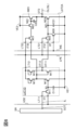
- 3A to 3C are circuit diagrams showing an example of a circuit included in the drive circuit.
- FIG. 4 is a circuit diagram showing an example of a circuit included in the drive circuit.
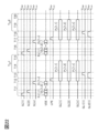
- 5A and 5B are timing charts showing an example of the operation of the circuits included in the drive circuit.
- FIG. 6 is a circuit diagram showing an example of a circuit included in the drive circuit.
- FIG. 7 is a circuit diagram showing an example of a circuit included in the drive circuit.
- FIG. 8 is a circuit diagram showing an example of a circuit included in the drive circuit.
- FIG. 9 is a circuit diagram showing an example of a circuit included in the drive circuit.
- FIG. 1 is a block diagram showing an example of a driving circuit.
- FIG. 2 is a block diagram showing an example of a driving circuit.
- 3A to 3C are circuit diagrams showing an example of
- FIG. 10 is a circuit diagram showing an example of a circuit included in the drive circuit.
- FIG. 11 is a circuit diagram showing an example of a circuit included in the drive circuit.
- FIG. 12 is a circuit diagram showing an example of a circuit included in the drive circuit.
- FIG. 13 is a circuit diagram showing an example of a circuit included in the drive circuit.
- FIG. 14 is a circuit diagram showing an example of a circuit included in the drive circuit.
- FIG. 15 is a circuit diagram showing an example of a circuit included in the drive circuit.
- FIG. 16 is a circuit diagram showing an example of a circuit included in the drive circuit.
- FIG. 17 is a circuit diagram showing an example of a circuit included in the drive circuit.
- FIG. 18 is a block diagram showing an example of a driving circuit.
- FIG. 11 is a circuit diagram showing an example of a circuit included in the drive circuit.
- FIG. 12 is a circuit diagram showing an example of a circuit included in the drive circuit.
- FIG. 13 is
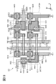
- FIG. 19 is a layout diagram showing an example of a driving circuit.
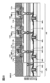
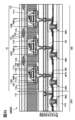
- 20A and 20B are schematic cross-sectional views showing configuration examples of a drive circuit.
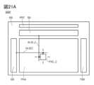
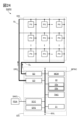
- FIG. 21A is a block diagram showing an example of the configuration of a display device
- FIG. 21B is a circuit diagram showing an example of the configuration of a pixel.
- FIG. 22 is a timing chart showing an example of the operation of the display device.
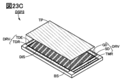
- 23A to 23C are schematic perspective views showing configuration examples of a display device.
- FIG. 24 is a block diagram showing an example of the configuration of a display device.
- FIG. 25 is a schematic cross-sectional view showing a configuration example of a display device.
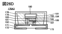
- 26A to 26D are schematic cross-sectional views showing configuration examples of an LED package.
- FIG. 27A and 27B are schematic plan views showing configuration examples of an LED package.
- FIG. 28A is a schematic cross-sectional view showing a configuration example of a display device
- FIG. 28B is a schematic cross-sectional view showing a configuration example of a substrate provided in the display device and a light-emitting diode on the substrate.
- FIG. 29 is a schematic cross-sectional view showing a configuration example of a display device.
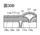
- 30A to 30C are schematic cross-sectional views showing a partial region of a configuration example of a display device.
- FIG. 31 is a schematic cross-sectional view showing a configuration example of a display device.
- FIG. 32 is a schematic cross-sectional view showing a configuration example of a display device.
- FIG. 33 is a schematic cross-sectional view showing a configuration example of a display device.
- 34A and 34B are diagrams showing a configuration example of a display module.
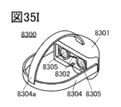
- 35A to 35I are perspective views showing an example of an electronic device.
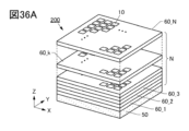
- FIG. 36A is a schematic perspective view illustrating a configuration example of a memory device
- FIG. 36B is a block diagram illustrating a configuration example of a semiconductor device.
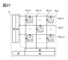
- FIG. 37 is a block diagram illustrating an example of the configuration of a storage device.
- 38A and 38B are diagrams illustrating an example of an electronic component.
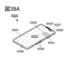
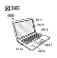
- 39A and 39B are diagrams showing an example of electronic equipment
- FIGS. 39C to 39E are diagrams showing an example of a mainframe computer.
- FIG. 40 is a diagram showing an example of space equipment.
- FIG. 41 is a diagram illustrating an example of a storage system applicable to a data center.
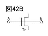
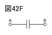
- 42A to 42I are diagrams explaining the "connection between A and B" in this specification.
- a semiconductor device is a device that utilizes semiconductor characteristics, and refers to a circuit including a semiconductor element (for example, a transistor, a diode, and a photodiode), or a device having such a circuit.
- a semiconductor device also refers to any device that can function by utilizing semiconductor characteristics.
- An example of a semiconductor device is an integrated circuit.
- Another example of a semiconductor device is a chip equipped with an integrated circuit, and another example of a semiconductor device is an electronic component that houses a chip in a package.
- a memory device, a display device, a light-emitting device, a lighting device, and an electronic device may themselves be semiconductor devices, or may have a semiconductor device.
- ordinal numbers such as “first”, “second”, and “third” are used to avoid confusion of components. Therefore, they do not limit the number of components. They also do not limit the order of components such as the process order and stacking order. In addition, even if a term does not have an ordinal number in this specification, an ordinal number may be added in the claims to avoid confusion of components. In addition, even if a term has an ordinal number in this specification, a different ordinal number may be added in the claims. In addition, even if a term has an ordinal number in this specification, the auxiliary number may be omitted in the claims.
- a component referred to by the ordinal number "first” in one embodiment of this specification may be a component referred to by a different ordinal number such as “second” or “third” in another embodiment or in the claims.
- a component referred to by the ordinal number "first” in one embodiment of this specification may be omitted in another embodiment or in the claims.
- the words “above” and “below” indicating position may be used for convenience in order to explain the positional relationship between components with reference to the drawings. Furthermore, the positional relationship between components changes as appropriate depending on the direction in which each configuration is depicted. Therefore, it is not limited to the words explained in the specification, but can be rephrased appropriately depending on the situation. For example, the expression “insulator located on the upper surface of a conductor” can be rephrased as "insulator located on the lower surface of a conductor” by rotating the orientation of the drawing shown by 180 degrees.
- the terms “above” and “below” do not limit the positional relationship of components to being directly above or below and in direct contact.
- the expression “electrode B on insulating layer A” does not require that electrode B be formed in direct contact with insulating layer A, and does not exclude other components between insulating layer A and electrode B.
- the expression “electrode B above insulating layer A” does not require that electrode B be formed in direct contact with insulating layer A, and does not exclude other components between insulating layer A and electrode B.
- the expression “electrode B below insulating layer A” does not require that electrode B be formed in direct contact below insulating layer A, and does not exclude other components between insulating layer A and electrode B.
- the terms “row” and “column” may be used to explain components arranged in a matrix and their relative positions. Furthermore, the relative positions of the components change as appropriate depending on the direction in which each configuration is depicted. Therefore, the terms are not limited to those described in the specification, and can be rephrased appropriately depending on the situation. For example, the expression “row direction” can sometimes be rephrased as “column direction” by rotating the orientation of the drawing shown by 90 degrees.
- the terms “film” and “layer” can be interchanged depending on the situation.
- the term “conductive layer” may be changed to the term “conductive film”.
- the term “insulating film” may be changed to the term “insulating layer”.
- the terms such as “film” and “layer” may not be used and may be replaced with other terms.
- the terms “conductive layer” or “conductive film” may be changed to the term “conductor”.
- the terms “insulating layer” or “insulating film” may be changed to the term "insulator”.
- electrode used in this specification and the like do not limit the functions of these components.
- an “electrode” may be used as a part of a “wiring,” and vice versa.
- the terms “electrode” and “wiring” include cases where multiple “electrodes” or “wirings” are formed integrally.
- a “terminal” may be used as a part of a “wiring” or “electrode,” and vice versa.
- terminal includes cases where one or more selected from “electrode,” “wiring,” and “terminal” are formed integrally.
- an “electrode” can be a part of a “wiring” or “terminal,” and, for example, a “terminal” can be a part of a “wiring” or “electrode.”
- the terms “electrode,” “wiring,” and “terminal” may be replaced with the term “region” depending on the circumstances.
- the terms “wiring”, “signal line” and “power line” may be interchangeable depending on the circumstances.
- the term “wiring” may be changed to "signal line”.
- the term “wiring” may be changed to "power line”.
- the opposite is also true, and terms such as “signal line” or “power line” may be changed to “wiring”.
- the term “power line” may be changed to "signal line”.
- the opposite is also true, and terms such as “signal line” may be changed to "power line”.
- the term “potential” applied to the wiring may be changed to "signal” depending on the circumstances. The opposite is also true, and the term “signal” may be changed to “potential”.
- a timing chart may be used to explain the operation method of a semiconductor device.
- the timing chart used in this specification shows an ideal operation example, and the period, the magnitude and timing of a signal (e.g., potential or current) described in the timing chart are not limited unless otherwise specified.
- the magnitude and timing of a signal (e.g., potential or current) input to each wiring (including a node) in the timing chart may be changed depending on the situation. For example, even if two periods are described in a timing chart at equal intervals, the lengths of the two periods may be different from each other.
- the lengths of both periods may be equal, or one period may be short and the other period may be long.
- two or more overlapping signals may be intentionally shifted.
- metal oxide is a metal oxide in a broad sense. Metal oxides are classified into oxide insulators, oxide conductors (including transparent oxide conductors), oxide semiconductors (also referred to as oxide semiconductors or simply OS), and the like. For example, when a metal oxide is included in the channel formation region of a transistor, the metal oxide may be referred to as an oxide semiconductor. In other words, when a metal oxide can constitute the channel formation region of a transistor having at least one of an amplification function, a rectification function, and a switching function, the metal oxide can be referred to as a metal oxide semiconductor. In addition, when an OS transistor is described, it can be rephrased as a transistor having a metal oxide or an oxide semiconductor.
- metal oxides containing nitrogen may also be collectively referred to as metal oxides.
- Metal oxides containing nitrogen may also be referred to as metal oxynitrides.
- impurities in a semiconductor refer to, for example, elements other than the main components constituting the semiconductor layer.
- an element with a concentration of less than 0.1 atomic % is an impurity.
- the inclusion of impurities may cause one or more of the following: an increase in the defect level density of the semiconductor, a decrease in carrier mobility, and a decrease in crystallinity.
- impurities that change the characteristics of the semiconductor include, for example, Group 1 elements, Group 2 elements, Group 13 elements, Group 14 elements, Group 15 elements, and transition metals other than the main components, and in particular, for example, hydrogen (also contained in water), lithium, sodium, silicon, boron, phosphorus, carbon, and nitrogen.
- parallel refers to a state in which two straight lines are arranged at an angle of -10 degrees or more and 10 degrees or less. Therefore, it also includes cases where the angle is -5 degrees or more and 5 degrees or less.
- substantially parallel or “roughly parallel” refers to a state in which two straight lines are arranged at an angle of -30 degrees or more and 30 degrees or less.
- perpendicular refers to a state in which two straight lines are arranged at an angle of 80 degrees or more and 100 degrees or less. Therefore, it also includes cases where the angle is 85 degrees or more and 95 degrees or less.
- substantially perpendicular or “approximately perpendicular” refers to a state in which two straight lines are arranged at an angle of 60 degrees or more and 120 degrees or less.
- the content described in one embodiment can be applied to, combined with, or substituted for at least one of the other content described in that embodiment (e.g., a part of another content) and the content described in one or more other embodiments (a part or all of the content).
- figure (in whole or in part) described in one embodiment can be combined with another portion of that figure, another figure (in whole or in part) described in that embodiment, and/or at least one figure (in whole or in part) described in one or more other embodiments to form even more figures.
- an identification number such as “_1”, “[n]”, “[m,n]” may be added to the reference number. Also, when an identification number such as “_1”, “[n]”, “[m,n]” is added to the reference number in the drawings, etc., when it is not necessary to distinguish between them in this specification, the identification number may not be added.
- ⁇ Driver Circuit Configuration Example 1> 1 is a block diagram illustrating a configuration example of a driver circuit according to one embodiment of the present invention. Note that the driver circuit functions as a source driver circuit in a display device.
- the drive circuit SD shown in FIG. 1 includes, as an example, a shift register SR, a circuit LAT1S, a circuit LAT2S, and a circuit LSHS.
- the shift register SR has, as an example, terminals SOT[1] to SOT[n] (n is an integer equal to or greater than 1) that function as output terminals.
- the circuit LAT1S has, as an example, holding circuits LAT1[1] to LAT1[n].
- Each of the circuits LAT1[1] to LAT1[n] has, for example, a terminal IT1, a terminal LT11, and a terminal LT12 that function as an input terminal.
- Each of the circuits LAT1[1] to LAT1[n] has, for example, a terminal OT11 and a terminal OT12 that function as an output terminal.
- the circuit LAT2S includes, as an example, holding circuits LAT2[1] to LAT2[n].
- Each of the circuits LAT2[1] to LAT2[n] has, as an example, terminals IT21, IT22, LT21, LT22, and RT that function as input terminals.
- Each of the circuits LAT1[1] to LAT1[n] has, as an example, terminal OT2 that functions as an output terminal.
- the circuit LSHS has, as an example, level shifters LSH[1] through LSH[n].
- Each of the level shifters LSH[1] through LSH[n] has, as an example, a terminal AT that functions as an input terminal. Also, each of the level shifters LSH[1] through LSH[n] has, as an example, a terminal ZT that functions as an output terminal.
- the terminal LT11 of the holding circuit LAT1[j] is connected to the terminal SOT[j] of the shift register SR via the wiring IL[j].
- the terminal IT1 of the holding circuit LAT1[j] is connected to the wiring VDE.
- the terminal LT12 of the holding circuit LAT1[j] is connected to the wiring LPE.
- the terminal OT11 of the holding circuit LAT1[j] is connected to the terminal IT21 of the holding circuit LAT2[j].
- the terminal OT12 of the holding circuit LAT1[j] is connected to the terminal IT22 of the holding circuit LAT2[j].
- Each of terminals LT21 and LT22 of the holding circuit LAT2[j] is connected to the wiring LPE.
- the terminal OT2 of the circuit LAT2[j] is connected to the terminal AT of the level shifter LSH[j] via the wiring OL[j].
- the terminal ZT of the level shifter LSH[j] is also connected to the wiring SL[j].
- the wiring VDE functions as a wiring for transmitting a first image signal. It is preferable that the first image signal is treated as a digital signal.
- the wiring LPE functions as a wiring that transmits a signal (sometimes referred to as a second pulse signal in this specification) for controlling the circuits LAT1[1] to LAT1[n] and the circuits LAT2[1] to LAT2[n].
- a signal sometimes referred to as a second pulse signal in this specification
- the second pulse signal functions as a latch pulse signal (sometimes referred to as a strobe signal) for the circuits LAT2[1] to LAT2[n], for example.
- the wiring INE functions as a wiring that transmits a signal to reset the image data stored in each of the circuits LAT2[1] to LAT2[n].
- the shift register SR for example, has holding circuits connected in series, and has the function of holding information corresponding to a signal input to the holding circuit, and the function of sequentially transmitting a signal corresponding to the information to an adjacent holding circuit.
- the shift register also, for example, has the function of outputting a signal (sometimes referred to as a first pulse signal in this specification) corresponding to the information held in the holding circuit to a terminal SOT.
- the signal that the shift register SR outputs to the terminal SOT corresponds to the strobe signal in the holding circuit LAT1.
- Each of the wirings IL[1] to IL[n] functions as a wiring for transmitting a first pulse signal (strobe signal) from the shift register SR to the holding circuit LAT1 as a control signal for capturing the first image signal transmitted to the wiring VDE, as an example.
- Each of the holding circuits LAT1[1] to LAT1[n] functions as a latch circuit, for example.
- a high-level potential is input as a first pulse signal from the terminal SOT of the shift register SR to the terminal LT11 of the holding circuit LAT1, causing the holding circuit LAT1 to hold a first potential corresponding to the first image signal and output a second image signal as the first potential to the terminal OT11 of the holding circuit LAT1.
- the logic of the first image signal and the second image signal are assumed to be equal.
- the holding circuit LAT1 blocks the input of the first image signal from the wiring VDE to the terminal IT1 of the holding circuit LAT1. At this time, the second image signal held at the first potential in the circuit LAT1 is continuously output to the output terminal OT11 of the holding circuit LAT1.
- the holding circuit LAT1 when a second pulse signal is transitioning from a low-level potential to a high-level potential from the line LPE to the terminal LT12 of the holding circuit LAT1, the holding circuit LAT1 outputs to the terminal OT12 a third image signal in which the logic of the first image signal (second image signal) corresponding to the held first potential is inverted.
- Each of the holding circuits LAT2[1] to LAT2[n] functions as a latch circuit, for example.
- a second image signal is transmitted from terminal OT11 of holding circuit LAT1 to terminal IT21 of holding circuit LAT2
- a third image signal in which the logic of the first image signal (second image signal) is inverted is transmitted from terminal OT12 of holding circuit LAT1 to terminal IT22 of holding circuit LAT2
- a second pulse signal is transmitted from line LPE to terminals LT21 and LT22 of holding circuit LAT2, respectively, from a low level potential to a high level potential, whereby holding circuit LAT2 holds a second potential corresponding to the second image signal and a third potential corresponding to the third image signal.
- holding circuit LAT2 generates a fourth image signal having the same logic as the third image signal based on the held second and third potentials, and outputs the fourth image signal to terminal OT2 of holding circuit LAT2.
- the holding circuit LAT2 blocks the input of the second image signal from the terminal OT11 of the holding circuit LAT1 to the terminal IT21 of the holding circuit LAT2, and blocks the input of the third image signal from the terminal OT12 of the holding circuit LAT1 to the terminal IT22 of the holding circuit LAT2.
- Each of the wirings OL[1] to OL[n] functions as a wiring for transmitting a fourth image signal from the holding circuit LAT2 to the level shifter LSH, for example.
- Each of the level shifters LSH[1] to LSH[n] has a function as a level shifter, for example.
- the level shifter LSH has a function of shifting the potential corresponding to the fourth image signal input from the terminal OT2 of the holding circuit LAT2 to the terminal AT of the level shifter LSH to another potential.
- the level shifter LSH when a high-level potential is input from the terminal OT2 of the holding circuit LAT2 to the terminal AT of the level shifter LSH, the level shifter LSH has a function of shifting the potential from the terminal ZT of the level shifter LSH to a potential higher than the high-level potential, or a potential higher than the low-level potential and lower than the high-level potential. Also, when a low-level potential is input from the terminal OT2 of the holding circuit LAT2 to the terminal AT of the level shifter LSH, the level shifter LSH has a function of outputting the low-level potential from the terminal ZT of the level shifter LSH.
- the level shifter LSH may have a function of shifting the potential from the terminal ZT of the level shifter LSH to a potential lower than the low-level potential, or a potential higher than the low-level potential and lower than the high-level potential. Also, when a high-level potential is input from the terminal OT2 of the holding circuit LAT2 to the terminal AT of the level shifter LSH, the level shifter LSH may have a function of outputting the high-level potential from the terminal ZT of the level shifter LSH.
- the level shifter LSH may have a function of shifting the potential from the terminal ZT of the level shifter LSH to a second high-level potential when a first high-level potential is input from the terminal OT2 of the holding circuit LAT2 to the terminal AT of the level shifter LSH, and a function of shifting the potential from the terminal ZT of the level shifter LSH to a second low-level potential when a first low-level potential is input from the terminal OT2 of the holding circuit LAT2 to the terminal AT of the level shifter LSH.
- the driver circuit SD shown in FIG. 2 is a modified example of the driver circuit SD in FIG. 1, and differs in configuration from the driver circuit SD in FIG. 1 in that the circuit LSHS is not provided and that the terminal OT2 of the holding circuit LAT[j] (not shown) is connected to the wiring SL[1]. If there is no need to level-shift the potential output from the terminal OT2 of the circuit LAT2, or if the circuit LAT2 includes a function as a level shifter, the driver circuit SD shown in FIG. 2 may be used in a display device.
- the circuit LAT1A shown in FIG. 3A is an example of a circuit configuration that can be applied to the circuit LAT1 included in the drive circuit SD in FIG. 1 or FIG. 2. Note that FIG. 3A also illustrates a shift register SR to show the peripheral connection configuration of the circuit LAT1A.
- the circuit LAT1A includes a transistor M11, a transistor M12, a transistor M13, and a capacitance element C11.
- an OS transistor for each of the transistors M11 to M13.
- examples of metal oxides contained in the channel formation region of an OS transistor include indium oxide, gallium oxide, and zinc oxide.
- the metal oxide has one or more types selected from indium, element M, and zinc.
- the element M is one or more types selected from gallium, aluminum, silicon, boron, yttrium, tin, copper, vanadium, beryllium, titanium, iron, nickel, germanium, zirconium, molybdenum, lanthanum, cerium, neodymium, hafnium, tantalum, tungsten, cobalt, magnesium, and antimony.
- the element M is one or more types selected from aluminum, gallium, yttrium, and tin.
- an oxide containing indium (In), gallium (Ga) and zinc (Zn) also referred to as IGZO
- it is preferable to use an oxide containing indium (In), aluminum (Al) and zinc (Zn) also referred to as IAZO
- it is preferable to use an oxide containing indium (In), aluminum (Al), gallium (Ga) and zinc (Zn) also referred to as IAGZO.
- the metal oxide used in the semiconductor layer has crystallinity.
- metal oxides having a CAAC (c-axis aligned crystal) structure, a polycrystalline (Poly-crystal) structure, a nanocrystalline (nc: nano-crystal) structure, or the like can be used in the semiconductor layer.
- the CAAC structure is a crystal structure in which multiple microcrystals (typically multiple IGZO microcrystals) have a c-axis orientation, and the multiple microcrystals are connected without being oriented in the a-b plane.
- the CAAC structure has fewer crystal grain boundaries and grains in the a-b plane than the polycrystalline structure, and therefore can realize a highly reliable driving circuit.
- the source electrode and drain electrode of transistors M11 to M13 are located at different heights, and that the current flowing through the semiconductor layer flows in the height direction.
- the channel length direction of transistors M11 to M13 has a component in the height direction (vertical direction).
- Such transistors can also be called VFETs (Vertical Field Effect Transistors), vertical transistors, vertical channel transistors, vertical channel transistors, etc. The structure of a VFET will be described in detail in embodiment 2.
- VFET As the structure of transistors M11 to M13, the area in which the transistors are formed can be reduced. Since a VFET can have a source electrode, semiconductor, and drain electrode that are stacked, the area it occupies can be significantly reduced compared to so-called planar transistors in which semiconductors are arranged in a plane. Therefore, by forming a driver circuit using transistors M11 to M13 to which a VFET structure is applied, the area of the driver circuit can be reduced. As a result, it is possible to reduce the size of a display device that includes the driver circuit.
- the channel length of a VFET can be made shorter than that of a planar transistor. Therefore, a VFET can have a larger on-current and a higher drive frequency than a planar transistor. Therefore, by forming a drive circuit using transistors M11 to M13, to which a VFET structure is applied, the drive speed of the drive circuit can be increased. This also makes it possible to increase the frame frequency of a display device including the drive circuit, and also enables PWM drive.
- Transistors other than OS transistors may be used as transistors M11 to M13.
- transistors having silicon in a channel formation region (hereinafter referred to as Si transistors) may be used as transistors M11 to M13.
- silicon for example, single crystal silicon, amorphous silicon, microcrystalline silicon, or polycrystalline silicon (including low temperature polycrystalline silicon (LTPS)) may be used.
- the transistors M11 to M13 may be, for example, transistors that contain germanium in their channel formation regions.
- a transistor that contains a compound semiconductor such as zinc selenide, cadmium sulfide, gallium arsenide, indium phosphide, gallium nitride, or silicon germanium in its channel formation region may be used.
- a transistor that contains a carbon nanotube in its channel formation region may be used.
- a transistor that contains an organic semiconductor in its channel formation region may be used.
- the gate of transistor M11 is connected to terminal LT11, and the first terminal of transistor M11 is connected to terminal IT1.
- the second terminal of transistor M11 is connected to the gate of transistor M13, the first terminal of capacitance element C11, and terminal OT11.
- the gate of transistor M12 and the first terminal of transistor M12 are each connected to terminal LT12. In this case, it can be said that the gate of transistor M12 and the first terminal of transistor M12 are electrically connected to each other.
- the second terminal of transistor M12 is connected to the first terminal of transistor M13 and terminal OT12.
- the second terminal of capacitance element C11 is connected to wiring VE1.
- the second terminal of transistor M13 is connected to wiring VE1.
- node N1 the connection point between the second terminal of transistor M11, the gate of transistor M13, the first terminal of capacitive element C11, and terminal OT11 is referred to as node N1.
- the wiring VE1 functions as a wiring that provides a fixed potential as a power source.
- the fixed potential can be, for example, a low-level potential, a ground potential, a negative potential, etc. Depending on the situation, the fixed potential may be a high-level potential, a positive potential, etc.
- the wiring VE1, for example, may function as a wiring that provides a variable potential (for example, a pulse voltage, a pulse signal, a clock signal, etc.) instead of a fixed potential.
- the fixed potential applied to the wiring VE1 is VLow . Also, in the initial operation, it is assumed that VLow is applied to the wiring LPE.
- a first pulse signal is provided as a control signal from the shift register SR to the terminal LT11 of the holding circuit LAT1A, that is, when the potential transitions from low-level potential VLow to high-level potential VHigh .
- the transistor M11 is turned on.
- a first image signal transmitted to the wiring VDE is input to the terminal IT1 of the holding circuit LAT1A.
- the potential of the first image signal is set to the high-level potential VHigh or the low-level potential VLow .
- the potential of the first image signal is VLow
- the potential of the node N1 becomes VLow .
- 0V is held between the first terminal and the second terminal of the capacitance element C11.
- VLow is applied to the gate of the transistor M13, and VLow is output to the terminal OT11 of the holding circuit LAT1A.
- the transistor M13 is turned off.
- Vth_M11 is the threshold voltage of the transistor M11.
- VHigh - VLow - Vth_M11 is held between the first terminal and the second terminal of the capacitance element C11.
- VHigh - Vth_M11 is applied to the gate of the transistor M13, and VHigh - Vth_M11 is output to the terminal OT11 of the holding circuit LAT1A.
- the gate-source voltage of the transistor M13 becomes VHigh - VLow - Vth_M11 .
- the gate-source voltage of the transistor M13 is a voltage that satisfies VHigh - VLow - Vth_M11 > Vth_M13 .
- the threshold voltage of the transistor M13 is V th_M13 . That is, the transistor M13 is in an on state.
- the on state of the transistor M13 at this time includes the case where the transistor M13 operates in a linear region and the case where the transistor M13 operates in a saturation region. Therefore, VLow provided by the wiring VE1 is output to the terminal OT12 of the circuit LAT1A.
- VLow the potential of the image signal input to the terminal IT1A of the holding circuit LAT1A is VLow
- VHigh - Vth_M12 is output as the third image signal to the terminal OT12 of the holding circuit LAT1A.
- Vth_M12 is the threshold voltage of the transistor M12.
- VLow is output as the third image signal to the terminal OT12 of the holding circuit LAT1A.
- the holding circuit LAT1A acquires the first image signal from the wiring VDE and holds a potential corresponding to the image signal in the capacitance element C11.
- the holding circuit LAT1A also outputs a second image signal to the terminal OT11 as a potential corresponding to the first image signal.
- the holding circuit LAT1A also outputs a third image signal, in which the logic of the first image signal is inverted, to the terminal OT12 as a second pulse signal when the wiring LPE transitions from a low-level potential VLow to a high-level potential VHigh .
- VLow is output from the terminal OT12.
- the wiring LPE functions as a wiring that supplies a variable potential (particularly, a pulse signal or a pulse potential) as a power supply potential to the circuits LAT1[1] to LAT1[n].
- V High is supplied as the second pulse signal to the wiring LPE
- the circuit configuration of the transistors M12 and M13 can be said to function as an inverter.
- the on-state current of the transistor M13 is preferably larger than the on-state current of the transistor M12.
- the on-state current of the transistor M13 is larger than the on-state current of the transistor M12, the amount of positive charge released from the terminal OT12 becomes larger than the amount of positive charge accumulated in the terminal OT12, and the potential of the terminal OT12 approaches the potential VLow provided by the wiring VE1. Therefore, the circuit configuration of the transistors M12 and M13 as an inverter can output a more accurate inverted signal.
- the circuit LAT1B shown in FIG. 3B is a modified example of the circuit LAT1A in FIG. 3A, and differs from the circuit LAT1A in FIG. 3A in that the gate of the transistor M12 is connected to the terminal OT12 instead of the terminal LT12. In this case, the gate of the transistor M12 can be said to be electrically connected to the first terminal of the transistor M12.
- the circuit LAT1B in FIG. 3B is configured as a holding circuit that operates favorably when the transistor M12 is normally on. For example, consider a case where the potential of the node N1 is a low-level potential VLow and the transistor M13 is in an off state. Also, since the transistor M12 is normally on, it is considered that the threshold voltage Vth_M12 of the transistor M12 is less than 0 V. At this time, a high-level potential VHigh is input to the wiring LPE as a second pulse signal, so that the potential of the terminal OT12 becomes VHigh .
- the threshold voltage Vth_M12 does not decrease between the source and drain of the transistor M12. That is, when the potential of the node N1 is a low-level potential VLow , the circuit configuration of the transistors M12 and M13 can output a high-level potential VHigh as an inverted signal of VLow .
- the potential of the terminal OT12 is the low-level potential VLow provided from the wiring VE1.
- the transistor M12 is normally on and therefore on.
- the potential of the terminal OT12 can be regarded as the low-level potential VLow if the on-current of the transistor M13 is larger than the on-current of the transistor M12.
- normally on refers to a state in which a channel exists and a current flows through the transistor even when the gate-source voltage is 0 V.
- normally off refers to a state in which no current flows through the transistor when the gate-source voltage is 0 V.
- normally off in an OS transistor refers to a state in which a current per 1 ⁇ m of channel width flowing through the transistor when the gate-source voltage is 0 V is 1 ⁇ 10 ⁇ 20 A or less at room temperature, 1 ⁇ 10 ⁇ 18 A or less at 85° C., or 1 ⁇ 10 ⁇ 16 A or less at 125° C.
- the circuit LAT1C shown in FIG. 3C is a modified version of the circuit LAT1A in FIG. 3A, and differs from the circuit LAT1A in FIG. 3A in that the gate of the transistor M12 is connected to the wiring VE2 instead of the terminal LT12, and that a transistor M14 has been newly provided.
- the gate of transistor M12 and the first terminal of transistor M12 are each connected to wiring VE2. Furthermore, the second terminal of transistor M12 and the first terminal of transistor M13 are each connected to the first terminal of transistor M14. Furthermore, the gate of transistor M14 is connected to terminal LT12, and the second terminal of transistor M14 is connected to terminal OT12.
- the wiring VE2 functions as a wiring that provides a fixed potential as a power source.
- the fixed potential can be, for example, a high-level potential, a positive potential, etc. Depending on the situation, the fixed potential may be a low-level potential, a ground potential, a negative potential, etc.
- the wiring VE2 may function as a wiring that provides a variable potential (for example, a pulse voltage, a pulse signal, a clock signal, etc.) instead of a fixed potential.
- the transistor M14 also functions as a switching element that controls whether or not the signal generated by the inverter is output to the terminal OT12. For example, when a high-level potential is input to the wiring LPE, the transistor M14 is turned on and the signal is output to the terminal OT12. On the other hand, when a low-level potential is input to the wiring LPE, the transistor M14 is turned off and the signal is not output to the terminal OT12.
- the holding circuit LAT2A shown in FIG. 4 is an example of a circuit configuration that can be applied to the holding circuit LAT2 included in the drive circuit SD in FIG. 1 or FIG. 2. Note that FIG. 4 also illustrates a shift register SR and a holding circuit LAT1A as an example to show the peripheral connection configuration of the holding circuit LAT2A.
- the holding circuit LAT1A in FIG. 3A is illustrated as the holding circuit LAT1 in FIG. 1 or FIG. 2, but the driving circuit of one embodiment of the present invention is not limited to this.
- the holding circuit LAT1A shown in FIG. 4 may be changed to the holding circuit LAT1B in FIG. 3B, or to the holding circuit LAT1C in FIG. 3C.
- the circuit LAT2A has a transistor M21, a transistor M22, a transistor M23, a transistor M24, a transistor M25, a transistor M26, a capacitance element C21, and a capacitance element C22.
- Each of the transistors M21 to M26 can be, for example, a transistor that can be applied to any one of the transistors M11 to M13.
- each of the transistors M21 to M26 can be an OS transistor having a VFET structure.
- the first terminal of transistor M21 is connected to terminal IT22, the gate of transistor M21 is connected to terminal LT22, and the second terminal of transistor M21 is connected to the first terminal of transistor M22.
- the second terminal of transistor M22 is connected to the gate of transistor M23 and the first terminal of capacitive element C22, and the gate of transistor M22 is connected to wiring VE2.
- the first terminal of transistor M23 is connected to wiring VE2.
- the first terminal of transistor M25 is connected to terminal IT21, the gate of transistor M25 is connected to terminal LT21, and the second terminal of transistor M25 is connected to the gate of transistor M24, the first terminal of transistor M26, and the first terminal of capacitance element C21.
- the first terminal of transistor M24 is connected to the second terminal of transistor M23, the first terminal of capacitance element C22, and terminal OT2.
- the gate of transistor M26 is connected to terminal RT, and the second terminal of transistor M26 is connected to wiring VE1.
- the second terminal of capacitance element C21 is connected to wiring VE1.
- the second terminal of transistor M24 is connected to wiring VE1.
- the region where the second terminal of transistor M25, the gate of transistor M24, the first terminal of transistor M26, and the first terminal of capacitance element C21 are connected is illustrated as node N21. Also, the region where the second terminal of transistor M22, the gate of transistor M23, and the first terminal of capacitance element C22 are connected is illustrated as node N22.
- wiring VE1 please refer to the explanation of wiring VE1 in FIG. 3A.
- wiring VE2 please refer to the explanation of wiring VE2 in FIG. 3C.
- FIG. 5A and 5B are timing charts showing examples of the operation of the holding circuits LAT1A and LAT2A, respectively.
- the timing chart of Fig. 5A shows an example of the operation when a high-level potential VHigh is input as an image signal from the wiring VDE to the holding circuit LAT1A
- the timing chart of Fig. 5B shows an example of the operation when a high-level potential VLow is input as an image signal from the wiring VDE to the holding circuit LAT2A.
- FIG. 5A and 5B shows the fluctuations in the potential of the wiring IL, wiring VDE, wiring LPE, wiring INE, wiring OL, node N1, node N21, and node N22 during the periods T1 to T3. Also, in each of Figures 5A and 5B, the period in which the potential is undefined or an arbitrary potential is input to a specific wiring or node is hatched.
- the potential applied by the wiring VE1 is VLow
- the potential applied by the wiring VE2 is VHigh
- VLow is applied to the wiring LPE as a low-level potential
- the transistors M21 and M25 are both off.
- an initialization operation is performed to set the potential of the node N21 to a low-level potential VLow .
- a high-level potential VHigh is applied to the wiring INE to turn on the transistor M26, thereby establishing electrical continuity between the node N21 and the wiring VE1, and the potential of the node N21 becomes the low-level potential VLow applied by the wiring VE1.
- a low-level potential VLow is applied to the wiring INE to turn off the transistor M26.
- a high-level potential VHigh is input as a first image signal from the wiring VDE to the terminal IT1 of the holding circuit LAT1A. Also, while the first image signal is being transmitted to the wiring VDE, a high-level potential VHigh is supplied as a first pulse signal (which may correspond to a strobe signal in the holding circuit LAT1A) to the terminal LT11 of the holding circuit LAT1A from the terminal SOT of the shift register SR via the wiring IL. This turns on the transistor M11, and the first image signal is transmitted to the holding circuit LAT1A.
- the holding circuit LAT1A outputs VHigh - Vth_M11 to the terminal OT11, and as a result, the potential of the first terminal of the transistor M25 becomes VHigh - Vth_M11 .
- the potential of the wiring LPE transitions from VLow to VHigh as the second pulse signal.
- the holding circuit LAT1A outputs VLow as the third image signal to the terminal OT12.
- the potential of the first terminal of the transistor M21 becomes VLow .
- the potential of the second pulse signal provided by the wiring LPE transitions from VLow to VHigh , turning the transistor M21 on.
- the potential of the second terminal of the transistor M21 becomes VLow .
- the transistor M22 Since the potential of the gate of the transistor M22 is VHigh , the transistor M22 is also in the on state, and thus VLow corresponding to the third image signal output from the terminal OT12 of the holding circuit LAT1A is written to the first terminal of the capacitance element C22.
- the potential of the second pulse signal provided by the wiring LPE transitions from VLow to VHigh , causing the potential of the gate of the transistor M25 to become VHigh .
- the potential of the first terminal of the transistor M25 is VHigh - Vth_M11
- the potential of the second terminal is VLow , so that the gate-source voltage of the transistor M25 becomes VHigh - VLow , and the transistor M25 is turned on.
- a second image signal corresponding to the potential of the node N1 is transmitted from the terminal OT11 of the holding circuit LAT1A to the terminal IT21 of the holding circuit LAT2A. Strictly speaking, charge is redistributed between the nodes N1 and N21.
- the potentials of the nodes N1 and N21 are set to V High -V th_M11 - ⁇ V due to the redistribution of charges.
- ⁇ V is a voltage higher than 0.
- ⁇ V is preferably as close to 0 as possible.
- the second pulse signal VHigh provided by the wiring LPE transitions to VLow , whereby the transistors M21 and M25 are each turned off, the potential VLow of the node N22 (potential corresponding to the third image signal) is held by the capacitance element C22, and the potential VHigh - Vth_M11 - ⁇ V of the node N21 (potential corresponding to the second image signal) is held by the capacitance element C21.
- the potential of the gate (node N22) of the transistor M24 is VHigh - Vth_M11 - ⁇ V. Furthermore, since the potential of the second terminal of the transistor M24 is VLow , the gate-source voltage of the transistor M24 can be expressed as VHigh - Vth_M11 - ⁇ V- VLow . Furthermore, VHigh - Vth_M11 - ⁇ V- VLow is higher than the threshold voltage of the transistor M24. Therefore, the transistor M24 is turned on, and the potential of the second terminal of the transistor M24 is VLow .
- the potential of the gate (node N21) of the transistor M23 is VLow . Since the potential of the second terminal of the transistor M23 is VLow , the gate-source voltage of the transistor M23 is 0 V, and the transistor M23 is turned off.
- the potential of the second terminal of the transistor M23 becomes VLow , and the holding circuit LAT2A outputs VLow to the terminal OT2 as a fourth image signal having the same logic as the third image signal.
- a low-level potential VLow is input as the first image signal from the wiring VDE to the terminal IT1 of the holding circuit LAT1A.
- a high-level potential VHigh is supplied as a first pulse signal (which may correspond to a strobe signal in the holding circuit LAT1A) to the terminal LT11 of the holding circuit LAT1A from the terminal SOT of the shift register SR via the wiring IL to the terminal LT11 of the holding circuit LAT1A. This turns on the transistor M11, and the first image signal is transmitted to the holding circuit LAT1A.
- the potential of the wiring LPE transitions from VLow to VHigh as the second pulse signal.
- the holding circuit LAT1A outputs VHigh - Vth_M12 as the third image signal to the terminal OT12.
- the potential of the first terminal of the transistor M21 becomes VHigh - Vth_M12 .
- the potential of the gate of the transistor M21 becomes VHigh as a result of the potential transition from VLow to VHigh as the second pulse signal provided by the wiring LPE. Furthermore, since VHigh - Vth_M12 is supplied to the first terminal of the transistor M21, the potential of the second terminal of the transistor M21 changes to a specific potential.
- the threshold voltage of the transistor M21 is Vth_M21 .
- VHigh - Vth_M12 is higher than VHigh - Vth_M21 , the potential of the second terminal of the transistor M21 becomes VHigh - Vth_M21 , and at this timing the transistor M21 is turned off.
- VHigh - Vth_M12 when VHigh - Vth_M12 is lower than VHigh - Vth_M21 , the potential of the second terminal of the transistor M21 becomes VHigh - Vth_M21 , and the transistor M21 continues to be on. In either case, in the following description, the potential of the second terminal of the transistor M21 is described as V2nd_M21 as a potential corresponding to the third image signal.
- the potential of the second terminal of the transistor M22 fluctuates to a specific potential.
- the threshold voltage of the transistor M22 is Vth_M22 .
- V2nd_M21 is higher than VHigh - Vth_M22
- the potential of the second terminal of the transistor M22 becomes VHigh - Vth_M21
- the transistor M22 is turned off at this timing.
- V2nd_M21 is lower than VHigh - Vth_M22
- the potential of the second terminal of the transistor M21 becomes V2nd_M21 , and the transistor M22 continues to be turned on.
- V 2nd_M22 the potential of the second terminal of the transistor M22
- the potential of the second pulse signal provided by the wiring LPE transitions from VLow to VHigh , causing the potential of the gate of the transistor M25 to become VHigh .
- the potential of the first terminal of the transistor M25 is VLow and the potential of the second terminal is VLow , so that the gate-source voltage of the transistor M25 becomes VHigh and the transistor M25 is turned on.
- a second image signal corresponding to the potential of the node N1 is transmitted from the terminal OT11 of the holding circuit LAT1A to the node N21. Strictly speaking, the potential of the node N21 remains at VLow and does not change from the initialization operation performed in the period T1.
- the potential of the gate (node N22) of the transistor M24 is VLow .
- the potential of the second terminal of the transistor M24 is VLow , the gate-source voltage of the transistor M24 is 0 V, and the transistor M24 is turned off.
- the transistor M23 since the potential of the gate (node N21) of the transistor M23 is V2nd_M22 , the transistor M23 is turned on, and a current flows from the wiring VE2 to the terminal OT2 through the transistor M23, and the potential of the terminal OT2 rises. At this time, since the node N21 is in a floating state, the potential of the node N21 also rises with the rise in the potential of the terminal OT2 due to the capacitive coupling of the capacitive element C21.
- the gate-source voltage of the transistor M23 is maintained by the capacitive element C21, so that the potential of the second terminal of the transistor M23 can be increased to the high-level potential VHigh provided by the wiring VE2.
- the operation of increasing the output voltage of a transistor while maintaining the gate-source voltage of the transistor constant using a capacitive element is called bootstrap.
- the voltage increased at the node N22 by the bootstrap is set to V BS , so the voltage at the node N22 becomes V 2nd_M22 +V BS .
- the potential of the second terminal of the transistor M23 becomes V High , and the holding circuit LAT2A outputs V High to the terminal OT2 as a fourth image signal having the same logic as the third image signal.
- a potential corresponding to the first image signal can be held in the holding circuit LAT1A and the holding circuit LAT1B, and a low-level potential can be output from the holding circuit LAT1B to the wiring OL (wiring SL) as a fourth image signal in which the logic of the first image signal is inverted.
- wiring SL wiring SL
- the holding circuits included in the driver circuit of one embodiment of the present invention are not limited to the configurations of the holding circuits LAT1A and LAT1B shown in FIG. 4.
- the holding circuit LAT1A shown in FIG. 4 can be changed to the configuration of the holding circuit LAT1D shown in FIG. 6.
- the holding circuit LAT1D in FIG. 6 is a modified example of the holding circuit LAT1A shown in FIG. 3A and FIG. 4, and differs from the holding circuit LAT1A in that it is provided with transistors M16 and M17.
- Each of the transistors M16 and M17 can be, for example, a transistor that can be applied to any one of the transistors M11 to M13.
- each of the transistors M16 and M17 can be an OS transistor having a VFET structure.
- the first terminal and the gate of transistor M16 are connected to the first terminal of transistor M12, the gate of transistor M12, and the terminal LT12. In this case, it can be said that the gate of transistor M16 is electrically connected to the first terminal of transistor M16.
- the second terminal of transistor M16 is connected to the first terminal of transistor M17 and the terminal OT11.
- the gate of transistor M17 is connected to the second terminal of transistor M12, the first terminal of transistor M13, and the terminal OT12.
- the second terminal of transistor M17 is connected to the wiring VE1.
- the holding circuits LAT1D and LAT2A in FIG. 6 apply a power supply voltage to the node N21 from the wiring LPE or the wiring VE1, so that it is possible to prevent fluctuations in the potential of the node N21 due to redistribution of charge that occurs in the holding circuits LAT1A and LAT2A in FIG. 4.
- the wiring VE21 functions as a wiring that supplies a high-level potential VHigh as a fixed potential
- the wiring VE22 preferably functions as a wiring that supplies a fixed potential that is higher or lower than the high-level potential VHigh .
- the potential supplied by the wiring VE22 rather than VHigh , can be output to the terminal OT2 of the holding circuit LAT1B.
- the circuit configuration of the transistors M12p and M13 can be an inverter of a CMOS circuit.
- the circuit configuration of the transistors M12p and M13 as an inverter of a CMOS circuit, in the holding circuit LAT1A of FIG. 4, when the potential of the node N1 is a low level potential, it is possible to prevent a decrease in the threshold voltage of the transistor M12 with respect to the high level potential output to the terminal OT12.
- n-channel transistors were changed to p-channel transistors in the holding circuits LAT1A and LAT1B shown in FIG. 4, but n-channel transistors may also be changed to p-channel transistors in other circuits described in this specification.
- the holding circuit LAT2B shown in FIG. 12 is an example of a circuit configuration that can be applied to the holding circuit LAT2 included in the drive circuit SD in FIG. 1 or FIG. 2. Note that FIG. 12 also illustrates a shift register SR and a holding circuit LAT1A as an example to show the peripheral connection configuration of the holding circuit LAT2B.
- the holding circuit LAT2B shown in FIG. 12 is a modified example of the holding circuit LAT2A shown in FIG. 4, and differs from the holding circuit LAT2A shown in FIG. 4 in that it does not include transistor M21 and that the gate of transistor M22 is connected to wiring LPE instead of wiring VE2.
- FIG. 12 an example of the operation of the holding circuits LAT1A and LAT2B shown in FIG. 12 will be described. Note that in this example, the operation of parts that differ from the holding circuits LAT1A and LAT2A in FIG. 4 will be described, and for other operations, refer to the operation in the timing charts of FIG. 5A and FIG. 5B.
- the gate of the transistor M22 When the low-level potential VLow is applied to the line LPE, the gate of the transistor M22 is supplied with VLow , and the transistor M22 is turned off.
- the gate of the transistor M22 When the high-level potential VHigh is applied to the line LPE as the second pulse signal, the gate of the transistor M22 is supplied with VHigh , and the transistor M22 is turned on.
- the third image signal output from the terminal OT12 of the holding circuit LAT1A is input to the first terminal of the transistor M22.
- VLow When the potential of the third image signal is VLow , VLow is written to the first terminal of the capacitance element C22.
- the potential written to the first terminal of the capacitance element C22 is determined according to the threshold voltage of the transistor M22. For example, when VHigh - Vth_M12 is higher than VHigh - Vth_M22 , VHigh - Vth_M22 is written to the first terminal of the capacitance element C22, and when VHigh - Vth_M12 is lower than VHigh - Vth_M22 , VHigh - Vth_M12 is written to the first terminal of the capacitance element C22.
- the potential of the wiring LPE is changed from the high-level potential VHigh to the low-level potential VLow , and the transistor M22 is turned off.
- VHigh - Vth_M12 when the potential corresponding to the third image signal output from the terminal OT12 of the holding circuit LAT1A is VHigh - Vth_M12 (when VLow is input to the terminal IT1 of the holding circuit LAT1A from the wiring VDE), VHigh - Vth_M22 or VHigh - Vth_M12 written to the first terminal of the capacitance element C22 corresponds to V2nd_M22 in the operation example of FIG. 5B.
- the holding circuit LAT2A in FIG. 4 is changed to the holding circuit LAT2B in FIG. 12, it is possible to hold a potential corresponding to the first image signal and output a fourth image signal in which the logic of the first image signal is inverted, just like the holding circuit LAT1A and holding circuit LAT2A in FIG. 4. Furthermore, since the holding circuit LAT2B in FIG. 12 does not have transistor M21, it has a smaller circuit area than the holding circuit LAT2A in FIG. 4. In other words, by applying the holding circuit LAT2B in FIG. 12 to the holding circuit LAT2 included in the drive circuit SD, the circuit area of the drive circuit SD can be reduced.
- the holding circuit LAT2C shown in Fig. 13 is an example of a circuit configuration that can be applied to the holding circuit LAT2 included in the drive circuit SD of Fig. 1 or 2, and is also a modified example of the holding circuit LAT2A shown in Fig. 4. Note that in order to show the peripheral connection configuration of the holding circuit LAT2C, a shift register SR and a holding circuit LAT1A are also shown in Fig. 13 as an example.
- the holding circuit LAT2C in FIG. 13 differs from the holding circuit LAT2A in FIG. 4 in that the gate of transistor M22 is connected to terminal IT22 instead of wiring VE2, the first terminal of transistor M22 is connected to wiring VE2, a transistor M27 is provided, and transistor M21 is not provided.
- Transistor M27 can be, for example, a transistor that can be applied to any one of transistors M11 to M13 and transistors M21 to M26 shown in FIG. 4.
- the gate of transistor M22 is connected to terminal IT22, and the first terminal of transistor M22 is connected to wiring VE2.
- the first terminal of transistor M27 is connected to the second terminal of transistor M22, the gate of transistor M23, and the first terminal of capacitance element C22.
- the second terminal of transistor M27 is connected to wiring VE1.
- the gate of transistor M27 is connected to the gate of transistor M24, the second terminal of transistor M25, the first terminal of transistor M26, and the first terminal of capacitance element C21.
- VHigh - Vth_M11 - ⁇ V is supplied to the gate of the transistor M27, turning on the transistor M27 and writing the low-level potential VLow from the wiring VE1 to the first terminal of the capacitance element C22.
- the transistor M23 is turned off and the transistor M24 is turned on, so that the holding circuit LAT2C outputs the low-level potential VLow to the terminal OT2 as the fourth image signal.
- the potential of the second pulse signal applied to the wiring LPE transitions from VLow to VHigh , turning on the transistor M25 and writing VLow to the first terminal of the capacitive element C21.
- VLow is applied to the gate of the transistor M27, turning off the transistor M27.
- the transistor M23 is turned on and the transistor M24 is turned off, so that the holding circuit LAT2C outputs a high-level potential V High as the fourth image signal to the terminal OT2.
- the holding circuit LAT2D shown in Fig. 14 is an example of a circuit configuration that can be applied to the holding circuit LAT2 included in the drive circuit SD in Fig. 1 or 2, and is also a modified example of the holding circuit LAT2C shown in Fig. 13. Note that Fig. 14 also illustrates a shift register SR and a holding circuit LAT1A as an example to show the peripheral connection configuration of the holding circuit LAT2D.
- the holding circuit LAT2D in FIG. 14 differs from the holding circuit LAT2C in FIG. 13 in that the first terminal of the transistor M22 is connected to the terminal IT22, not to the wiring VE2.
- the transistor M22 is configured as a diode connection.
- the transistor M23 is turned on and the transistor M24 is turned off, so that the holding circuit LAT2C outputs the high-level potential V High to the terminal OT2 as the fourth image signal.
- transistor M24 is turned on, and thus holding circuit LAT2E outputs a low-level potential to line OL as the fourth image signal. At this time, the low-level potential is input to the gate of transistor M28. As a result, transistor M28 is turned off. Therefore, in the example of operation in FIG. 5A, there is no change due to the provision of transistor M28.
- Transistor M29 can be, for example, a transistor that can be applied to any one of transistors M11 to M13 and transistors M21 to M26 shown in FIG. 4.
- the first terminal of transistor M29 is connected to the second terminal of transistor M21 and the first terminal of transistor M22.
- the second terminal of transistor M29 is connected to wiring VE1.
- the gate of transistor M29 is connected to the gate of transistor M24, the second terminal of transistor M25, the first terminal of transistor M26, and the first terminal of capacitance element C21.
- the potential of the node N22 is ideally preferably set to the low-level potential VLow .
- the transistor M12 since the transistor M12 is also turned on, the potential of the node N22 may become higher than the low-level potential VLow .
- a transistor M29 is provided as in the holding circuit LAT2G of Fig. 17.
- the transistor M25 is turned on, and VHigh - Vth_M11 - ⁇ V is applied to the node N21.
- the transistor M29 is turned on, and electrical continuity is established between the second terminal of the transistor M21 and the first terminal of the transistor M22 and the wiring VE1.
- the potentials of the second terminal of the transistor M21 and the first terminal of the transistor M22 become VLow , and the potential of the node N22 can be set to VLow .
- FIG. 18 is a block diagram showing a configuration example of a driver circuit according to one embodiment of the present invention that is different from that shown in FIG. 1. Note that the driver circuit has a function as a source driver circuit in a display device.
- the circuit LATS includes holding circuits LATX[1] through LATX[n], holding circuits LATY[1] through LATY[n], switches SW0[1] through SW0[n], switches SW1X[1] through SW1X[n], and switches SW1Y[1] through SW1Y[n].
- Each of the switches SW0[1] to SW0[n], the switches SW1X[1] to SW1X[n], and the switches SW1Y[1] to SW1Y[n] may be, for example, an electrical switch (e.g., a transistor, an analog switch, etc.) or a mechanical switch.
- one of the electrical switches may be a transistor that can be any one of the transistors M11 to M13 and the transistors M21 to M26 shown in FIG. 4.
- the transistor is, for example, an OS transistor.
- each of the holding circuits LAT Y[1] to LAT Y[n] has, as an example, a terminal IT1, a terminal LT11, and a terminal LT12 that function as an input terminal. Also, each of the holding circuits LAT Y[1] to LAT Y[n] has, as an example, a terminal OT12 that functions as an output terminal.
- holding circuits LATX[1] through LATX[n] and the holding circuits LATTY[1] through LATTY[n] can each have the same circuit configuration.
- the second terminal of the switch SW1X[j] and the second terminal of the switch SW1Y[j] are each connected to the terminal AT of the level shifter LSH[j].
- the terminal ZT of the level shifter LSH[j] is connected to the line SL[j].
- the wiring VDE has a function as a wiring for transmitting a first image signal, similar to the wiring VDE shown in FIG. 1, as an example. Note that it is preferable that the first image signal is treated as a digital signal.
- the wirings LPE1 and LPE2 function as wirings that transmit signals for controlling the holding circuits LATX[1] to LATX[n], the holding circuits LATY[1] to LATY[n], the switches SW1X[1] to SW1X[n], and the switches SW1Y[1] to SW1Y[n]. Note that while the circuit LATS is operating, it is preferable that a signal with the logic of the signal transmitted to the wiring LPE1 be inverted is transmitted to the wiring LPE2.
- the signal has a function as a strobe signal (sometimes called a latch pulse signal) for the holding circuits LATX[1] through LATX[n], and a function as a wiring that transmits a control signal for switching between the on and off states of the switches SW1Y[1] through SW1Y[n].
- the strobe signal and the control signal are treated as the same signal.
- the signal has a function as a strobe signal (sometimes called a latch pulse signal) for the holding circuits LAT Y[1] to LAT Y[n], and a function as a wiring that transmits a control signal for switching between the on and off states of the switches SW1X[1] to SW1X[n].
- the strobe signal and the control signal are treated as the same signal.
- Each of the holding circuits LATX[1] to LATX[n] and the holding circuits LATTY[1] to LATTY[n] functions as a latch circuit, as with the holding circuit LAT1, for example.
- each of the holding circuits LATX[1] to LATX[n] and the holding circuits LATTY[1] to LATTY[n] can be any one of the holding circuits LAT1A to LAT1C shown in Figures 3A to 3C.
- the holding circuit LAT1C of FIG. 3C when the holding circuit LAT1C of FIG. 3C is applied to each of the holding circuits LATX[1] to LATX[n] and the holding circuits LATTY[1] to LATTY[n], the switches SW1X[1] to SW1X[n] and the switches SW1Y[1] to SW1Y[n] do not need to be provided in the circuit LATS.
- the terminal OT12 of the holding circuit LATX[j] and the terminal OT12 of the holding circuit LATTY[j] may each be directly connected to the level shifter LSH[1].
- a first image signal is sent from the wiring VDE to the terminal IT1 via the switch SW0 and a high-level potential is applied as a strobe signal to the terminal LT11 from one of the wiring LPE1 and wiring LPE2, a potential corresponding to the first image signal is acquired in one of the holding circuits LATX and LATY. Also, at this time, while a low-level potential is applied to the terminal LT12 from the other of the wiring LPE1 and wiring LPE2, the terminal OT12 does not output a potential corresponding to the first image signal.
- one of the holding circuits LATX and LATY holds a potential corresponding to the first image signal captured at terminal IT1. Therefore, even if the potential of another first image signal is input to terminal IT1 of one of the holding circuits LATX and LATY, one of the holding circuits LATX and LATY does not capture the other first image signal.
- a third image signal in which the logic of the first image signal held in one of the holding circuits LATX and LATY is inverted is output from terminal OT12 of one of the holding circuits LATX and LATY.
- a high-level potential is input from the other of the wirings LPE1 and LPE2 to one of the control terminals of the switches SW1X and SW1Y, so one of the switches SW1X and SW1Y is in the on state. Therefore, the third image signal output from one of the terminals OT12 of the holding circuits LATX and LATEY is input to the level shifter LSH.
- holding circuit LATX[j] does not capture the first image signal transmitted from wiring VDE to terminal LT11 via switch SW0[1].
- holding circuit LATX[j] outputs a third image signal, which is the inverted logic of the first image signal held by holding circuit LATX[j], to terminal OT12.
- switch SW1Y[j] since switch SW1Y[j] is in the on state, the third image signal is transmitted to terminal AT of level shifter LSH[j].
- the driver circuit SD in FIG. 1 and FIG. 2 the holding circuits LAT1 and LAT2 functioning as latch circuits are connected in series, but the driver circuit of one embodiment of the present invention may be configured as shown in FIG. 18, in which the holding circuits LATX and LATY functioning as latch circuits are connected in parallel.
- the number of transistors, the number of capacitors, and the number of wirings may be reduced compared to the driver circuit SD in FIG. 1 and FIG. 2. Therefore, by applying the configuration shown in FIG. 18 as one embodiment of the present invention, the area of the driver circuit may be reduced.
- FIG. 19 is a layout diagram (plan view) of the holding circuit LAT1A and the holding circuit LAT2A shown in FIG. 4.
- each of the transistors M11 to M13 and the transistors M21 to M26 is configured as a VFET (vertical channel transistor).
- the left-right direction of the drawing is the X direction
- the up-down direction of the drawing is the Y direction.
- the direction perpendicular to the X and Y directions is the Z direction.
- the X and Y directions can be perpendicular to each other.
- the definitions of the X, Y, and Z directions may be the same or different in subsequent drawings.
- the right side may be referred to as the X direction, the left side as the -X direction, the upper side as the Y direction, and the lower side as the -Y direction.
- the right side may be referred to as the X direction, the left side as the -X direction, the upper side as the Z direction, and the lower side as the -Z direction.
- the semiconductor layer SC1 is located below the conductive layer ME3.
- the conductive layer ME2 is located below the semiconductor layer SC1.
- the conductive layer ME1 is located below the conductive layer ME2.
- the holding circuit LAT1A and the holding circuit LAT2A are respectively formed in the order of conductive layer ME1, conductive layer ME2, semiconductor layer SC1, and conductive layer ME3 from the bottom.
- the conductive layer ME2 has regions that function as the source or drain of each of the transistors M11 to M13 and the transistors M21 to M26.
- the conductive layer ME2 also has regions that function as wiring.
- the conductive layer ME2 has a region that functions as wiring VE1 and a region that functions as wiring VE2.
- the insulating layer IS3 functions as a barrier insulating film to prevent the diffusion of impurities into the transistors M13, M24, and M25.
- the insulating layer IS3 functions as a base film or an interlayer film for providing the circuit element.
- transistors M13, M24, and M25 can be either p-channel or n-channel.
- the channel length of each of transistors M13, M24, and M25 can be, for example, 5 nm or more, 7 nm or more, 10 nm or more, 20 nm or more, 30 nm or more, or 50 nm or more, and 3 ⁇ m or less, 2.5 ⁇ m or less, 2 ⁇ m or less, 1.5 ⁇ m or less, 1.2 ⁇ m or less, 1 ⁇ m or less, 500 nm or less, 300 nm or less, 200 nm or less, 100 nm or less, 50 nm or less, 30 nm or less, or 20 nm or less.
- the channel length can be 5 nm or more and 3 ⁇ m or less, or 50 nm or more and 150 nm or less.
- the pixel array PXA has, as an example, a plurality of pixel circuits PX.
- the plurality of pixel circuits PX are arranged in an array in the pixel array PXA.
- the plurality of pixel circuits PX are arranged in any one of a matrix arrangement, a stripe arrangement, an S-stripe arrangement, a delta arrangement, a Bayer arrangement, a Pentile arrangement, etc.
- the pixel circuit PX located in the i-th row and j-th column (i is an integer of 1 or more, and j is an integer of 1 or more) is represented as pixel circuit PX[i, j].
- the drive circuit GD functions, for example, as a gate driver circuit for selecting a pixel circuit PX included in the pixel array PXA to which an image signal is to be written.
- the pixel circuit PX[i,j] is, for example, electrically connected to the drive circuit GD via the wiring GLS[i]. Also, the pixel circuit PX[i,j] is, for example, electrically connected to the drive circuit SD via the wiring SLS[j].
- the wiring SLS[i] functions as a wiring for transmitting an image signal from the drive circuit SD to the pixel circuit PX[i,j] to display an image in the pixel circuit PX[i,j].
- the wiring GLS[i] may be a single wiring or a wiring group consisting of multiple wirings.
- the wiring SLS[j] may be a single wiring or a wiring group consisting of multiple wirings.
- the drive circuit TSD functions as a circuit for driving a touch sensor provided in an area overlapping the pixel array PXA in a planar view. Note that if a touch sensor is not provided in that area, the display device DSP does not need to be provided with a drive circuit TSD.
- the protection circuit PRT is electrically connected to the wiring GLS[i] and another wiring.
- the protection circuit PRT has a function of bringing the wiring GLS[i] and the other wiring into a conductive state, thereby keeping the potential of the wiring GLS[i] within a predetermined range.
- the protection circuit PRT may be electrically connected to the wiring SLS[j] and another wiring.
- the protection circuit PRT has a function of, for example, when a potential outside a predetermined range is applied to the wiring SLS[j], bringing the wiring SLS[j] and the other wiring into a conductive state, thereby keeping the potential of the wiring SLS[j] within a predetermined range.
- the pixel circuit PX shown in FIG. 21B is an example of a circuit configuration that can be applied to the pixel circuit PX[i,j] shown in FIG. 21A.
- the pixel circuit PX in FIG. 21B has a transistor M01, a transistor M02, a transistor M03, a capacitive element C01, and a light-emitting device ED.
- Each of the transistors M01 to M03 can be, for example, a transistor that can be applied to any one of the transistors M11 to M13 and the transistors M21 to M26 shown in FIG. 4.
- the transistor M02 corresponds to the driving transistor of the pixel circuit PX. Since light-emitting devices that include micro LEDs are extremely resistant to degradation compared to light-emitting devices that include organic EL materials, the transistor M02 can be operated not only in the saturation region but also in the linear region when in the on state.
- the light emitting device ED has an anode terminal and a cathode terminal, for example.
- the light emitting device ED can be a light emitting diode such as a micro LED.
- the light emitting device ED can be a light emitting device using an organic electroluminescent material (sometimes called an OLED) other than a light emitting diode such as a micro LED.
- OLED organic electroluminescent material
- the light emitting device ED will be described as a light emitting diode such as a micro LED, for example.
- the first terminal of the transistor M01 is connected to the wiring SL, the second terminal of the transistor M01 is connected to the gate of the transistor M02 and the first terminal of the capacitance element C01, and the gate of the transistor M01 is connected to the wiring GL1.
- the first terminal of the transistor M02 is connected to the wiring VA, and the second terminal of the transistor M02 is connected to the first terminal of the transistor M03 and the anode of the light-emitting device ED.
- the second terminal of the transistor M03 is connected to the wiring VRS, and the gate of the transistor M03 is connected to the wiring GL2.
- the cathode of the light-emitting device ED is connected to the wiring VC.
- the second terminal of the capacitance element C01 is connected to the wiring VE0.
- the wiring SL shown in FIG. 21B corresponds to the wiring SLS[j] shown in FIG. 21A.
- the wiring SL functions as a wiring for transmitting an image signal from the driving circuit SD to the pixel circuit PX.
- the wiring GL1 and wiring GL2 shown in FIG. 21B correspond to the wiring GLS[i] shown in FIG. 21A.
- the wiring GL1 and wiring GL2 function as wirings for transmitting a selection signal for driving the pixel circuit PX.
- the wiring VE0 has a function as a wiring that provides a fixed potential.
- the fixed potential can be, for example, a low-level potential, a ground potential, a negative potential, etc. Furthermore, depending on the situation, the fixed potential may be a high-level potential, a positive potential, etc.
- the wiring VE0 for example, may have a function as a wiring that provides a variable potential (for example, a pulse voltage, a pulse signal, a clock signal, etc.) instead of a fixed potential.
- Each of the wiring VA, wiring VRS, and wiring VC functions as a wiring that provides a fixed potential as a power source.
- the wiring VA is preferably a wiring that supplies an anode potential to be applied to the anode of the light-emitting device ED.
- the wiring VC is preferably a wiring that supplies a cathode potential to be applied to the cathode of the light-emitting device ED.
- the wiring VRS functions as a wiring that provides a fixed potential to the second terminal of the transistor M02, the first terminal of the transistor M03, and the anode of the light-emitting device ED.
- the fixed potential may be called a reset potential.
- the image signal written to the pixel circuit PX can be, for example, the fourth image signal output from terminal OT2 of the holding circuit LAT2 of the drive circuit SD, as described in the above embodiment.
- a high-level potential is applied to the wiring GL2 to turn on the transistor M03.
- the potentials of the second terminal of the transistor M02, the first terminal of the transistor M03, and the anode of the light-emitting device ED are set to the reset potential. This makes it possible to write a potential corresponding to an image signal to the gate of the transistor M02 while stabilizing the source potential of the transistor M02.
- a fourth image signal is sent to the wiring SL to be written to the gate of the transistor M02 of the pixel circuit PX.
- a high-level potential is applied to the wiring GL1 to turn on the transistor M01.
- the potentials of the gate of the transistor M02 and the first terminal of the capacitance element C01 become a potential corresponding to the fourth image signal.
- a current flows from the wiring VA through the anode and cathode of the light-emitting device ED to the wiring VC.
- the amount of current flowing between the anode and cathode of the light-emitting device ED is determined by the respective potentials of the gate of the transistor M02 and the wiring VA.
- the pixel circuit according to one embodiment of the present invention is not limited to the pixel circuit PX shown in FIG. 21B.
- a pixel circuit capable of correcting the threshold voltage of the transistor M02 may be used (not shown).
- a method of controlling the gradation by defining periods of subframes that emit light and subframes that do not emit light within one frame is preferable.
- FIG. 22 is a timing chart showing an example of the operation of the display device DSP of FIG. 21A. Note that the display device DSP of FIG. 21A uses the drive circuit SD of FIG. 1 or FIG. 2 as the drive circuit SD.
- the timing chart in FIG. 22 shows changes in the potentials of the wirings IL[1], IL[2], IL[n], LPE, GL1[1], and GL2[1] during the operation of writing image data to the display device DSP.
- the timing chart in FIG. 22 also shows signals transmitted to the wirings VDE, SL[1], SL[2], and SL[n].
- periods T11 to T15 and periods T16 to T16 are each a subframe period.
- the shift register SR illustrated in FIG. 1 or 2 sequentially outputs a high-level potential V High as a first pulse signal from each of the terminals SOT[1] to SOT[n].
- digital data D1[1,1] to D1[1,n] are sequentially transmitted to the wiring VDE as the first image signal at the timing when the high-level potential VHigh is sequentially output from each of the terminals SOT[1] to SOT[n] as the first pulse signal.
- D1 [1,1], D1 [1,2], and D1 [1,n] are selectively illustrated in FIG. 22.
- the digital data D1 [1,1] to D1 [1 , n] are written and retained in each of the holding circuits LAT1 [1] to LAT1[n] illustrated in FIG. 1 or FIG. 2.
- the digital data is data for putting the light emitting device ED included in the pixel circuit PX into one of a light emitting state and a non-light emitting state. Therefore, as an example, the potential according to the digital data can be V High or V Low .
- the pixel circuit PX performs an initialization operation and writes digital data as the fourth image signal. Specifically, first, a high-level potential is input to the wiring GL2[1], and the pixel circuit PX is initialized. Next, a high-level potential is input to the wiring GL1[1], and digital data corresponding to the fourth image signal transmitted to the wiring SL is written to the pixel circuit PX.
- digital data P1 [1,1] transmitted to the line SL[1] is written to the pixel circuit PX[1,1].
- digital data P1 [1,2] transmitted to the line SL[2] is written to the pixel circuit PX[1,2].
- digital data P1[1,n] corresponding to a fourth image signal transmitted to the line SL[n] is written to the pixel circuit PX [1,n].
- a predetermined first image signal is written to each of the holding circuits LAT1[1] to LAT1[n] in the same manner as the operation in the period T11 (not shown in FIG. 22).
- the holding circuits LAT2[1] to LAT2[n] output the digital data P 1 [1,1] to P 1 [1,n] as the fourth image signal from their respective terminals OT2.
- period T15 digital data corresponding to image data is written to pixel circuits PX from the second row to the mth row of the pixel array PXA by the same operation as that from period T12 to period T14.
- digital data corresponding to image data can be written to all pixel circuits PX arranged in the pixel array PXA of the display device DSP. This makes it possible to display an image in the pixel array PXA of the display device DSP.
- a write operation of digital data corresponding to image data is performed to pixel circuits PX from the 1st row to the mth row of the pixel array PXA.
- a write operation of digital data corresponding to image data is performed to pixel circuits PX from the 1st row to the mth row of the pixel array PXA.
- period T16 an operation similar to that of period T11 is performed, in period T17, an operation similar to that of period T12 is performed, in period T18, an operation similar to that of period T13 is performed, in period T19, an operation similar to that of period T14 is performed, and in period T20, an operation similar to that of period T15 is performed.
- digital data D2 [1,1] to D2 [1,n] are transmitted as image data to the wiring VDE as a first image signal, and as a result, during period T18, digital data P2[1,1] to P2[1,n], which is obtained by inverting the logic of D2 [1,1] to D2 [1,n], are written to the pixel circuits PX [1,1] to PX [1,n].
- digital data corresponding to the image data is written to the pixel circuits PX from the second row to the m-th row of the pixel array PXA, thereby enabling an image to be displayed on the pixel array PXA of the display device DSP.
- a method of controlling the gradation by determining the period of a subframe in which light is emitted and a subframe in which light is not emitted within one frame is preferable. Therefore, when controlling the gradation in the operation example shown in the timing chart of FIG. 22, it is preferable to adjust, for example, the time of the period T ED 1, which is a combination of the period T14 and the period T15 in which an image is displayed, and the time of the period T ED 2, which is a combination of the period T19 and the period T20 in which an image is displayed. For example, by making the time of the period T ED 1 and the time of the period T ED 2 1:2, the gradation in the image display can be expressed in four stages: 0, 1, 2, and 3.
- the widths of the pulse signals transmitted to the wirings IL[1] to IL[n], the wiring LPE, the wiring GL1[1], and the wiring GL2[1] may be adjusted.
- the gray scale of the image display can be expressed in four levels, 0, 1, 2, and 3.
- the degree of gradation can be determined for the image displayed on the display device DSP.
- the drive circuit SD provided in the display device DSP requires a holding circuit capable of operating at a high drive frequency.
- FIG. 23A is a schematic perspective view showing a display device according to one embodiment of the present invention.
- the display device DSP1 has a display region DIS, a drive circuit region DRV, and a terminal region TMR.
- the display device DSP1 also has a substrate BS, and the display region DIS, the drive circuit region DRV, and the terminal region TMR are each located on the substrate BS.
- the display region DIS can include, for example, the pixel array PXA of FIG. 21A described in embodiment 3.
- the drive circuit region DRV also includes, as an example, drive circuits GD1, GD2, and SD. Note that drive circuits GD1 and GD2 correspond to the drive circuit GD in FIG. 21A described in embodiment 3, for example, and drive circuit SD corresponds to the drive circuit SD in FIG. 21A described in embodiment 3, for example.
- the substrate BS may be, for example, a semiconductor substrate (e.g., a single crystal substrate made of silicon or germanium).
- the substrate BS may be, for example, an SOI substrate, a glass substrate, a quartz substrate, a plastic substrate, a sapphire glass substrate, a metal substrate, a stainless steel substrate, a substrate having stainless steel foil, a tungsten substrate, a substrate having tungsten foil, a flexible substrate, a laminated film, or a paper or base film containing a fibrous material.
- glass substrates include, for example, barium borosilicate glass, aluminoborosilicate glass, or soda lime glass.
- Examples of flexible substrates, laminated films, base films, and the like include plastics such as polyethylene terephthalate (PET), polyethylene naphthalate (PEN), polyethersulfone (PES), and polytetrafluoroethylene (PTFE).
- PET polyethylene terephthalate
- PEN polyethylene naphthalate
- PES polyethersulfone
- PTFE polytetrafluoroethylene
- Another example is a synthetic resin such as an acrylic resin.
- Another example is polypropylene, polyester, polyvinyl fluoride, or polyvinyl chloride.
- Other examples include polyamide, polyimide, aramid, epoxy resin, inorganic vapor deposition film, and paper. If the manufacturing process of the display device DSP1 includes a heat treatment, it is preferable to use a material with high heat resistance for the substrate BS.
- the transistors included in the display area DIS and the drive circuit area DRV can be formed as Si transistors on the substrate BS.
- the transistors included in the display region DIS and the drive circuit region DRV can be formed on the substrate BS as OS transistors.
- Each of the drive circuits GD1 and GD2 functions, for example, as a drive circuit for displaying an image in the display area DIS. Specifically, for example, each of the drive circuits GD1 and GD2 functions as a gate driver circuit for the display area DIS. Also, for example, the drive circuit SD functions as a source driver circuit for the display area DIS.
- the display area DIS has, as an example, a plurality of pixels. Furthermore, the plurality of pixels may be arranged in a matrix in the display area DIS.
- the multiple pixels may be pixel circuits that use one or more of a liquid crystal display device, a light-emitting device including an organic EL material, a light-emitting device including an inorganic EL material, and a light-emitting device including a light-emitting diode such as a micro LED.
- the display device of one embodiment of the present invention is not limited to the configuration of the display device DSP1 illustrated in FIG. 23A.
- the display device of one embodiment of the present invention may have the configuration of the display device DSP2 illustrated in FIG. 23B.
- the display device DSP2 shown in FIG. 23B has, as an example, a display area DIS, a circuit area SIC, and a terminal area TMR.
- the display device DSP2 also has a substrate BS, similar to the display device DSP1.
- the display device DSP2 differs from the display area DSP1 in that the circuit area SIC and the terminal area TMR are provided on the substrate BS, and the display area DIS is provided on the circuit area SIC.
- the EL correction circuit monitors the amount of current flowing through the light-emitting device, and when the amount of current is smaller than the desired amount of current, increases the amount of current flowing through the light-emitting device, thereby increasing the brightness of the light emitted by the light-emitting device. Conversely, when the amount of current is larger than the desired amount of current, the amount of current flowing through the light-emitting device may be adjusted to be smaller.
- the functional circuit area MFNC may also include a gamma correction circuit.
- FIG. 24 is a block diagram showing an example of the configuration of the display device DSP2 shown in FIG. 23B.
- the display device DSP2 shown in FIG. 24 has, as an example, a display area DIS and a circuit area SIC. Also, while FIG. 24 shows a sensor PDA, the sensor PDA may be disposed inside or outside the display device DSP2.
- the display device DSP1 in FIG. 23A may also be connected to a functional circuit region MFNC located outside the display device DSP1 via a terminal region TMR.
- the configuration of the display device DSP1 in this case can be considered to be the same as the configuration of the display device DSP2 shown in FIG. 24.
- a plurality of pixel circuits PX are arranged in a matrix in the display area DIS.
- the pixel circuits PX arranged in a matrix can be considered to be included in the pixel array PXA shown in FIG. 21A described in the third embodiment above.
- the circuit region SIC has a drive circuit region DRV and a functional circuit region MFNC, as described above.
- the functional circuit area MFNC may be provided with circuits such as a memory device in which image data to be displayed in the display area DIS is stored, a decoder for restoring encoded image data, a GPU for processing image data, a power supply circuit, a correction circuit, or a CPU (Central Processing Unit).
- the functional circuit area MFNC has, as an example, a memory device MEM, a GPU 22, a timing controller TMC, a CPU (NoffCPU (registered trademark)) 21, a sensor controller SCC, and a power supply circuit EPS.
- the drive circuit SD has a function of transmitting image data to the pixel circuits PX included in the display area DIS. For this reason, the drive circuit SD is connected to the pixel circuits PX via wiring SL. Note that the arrow near the wiring SL indicates the direction in which the image data is transmitted.
- the drive circuit region DRV includes a digital-analog conversion circuit.
- the digital-analog conversion circuit has a function of converting image data digitally processed by the GPU or correction circuit described below into analog data.
- the image data converted into analog data is transmitted to the display region DIS via the drive circuit SD.
- the digital-analog conversion circuit may be included in the drive circuit SD, or the image data may be transmitted in the order of the drive circuit SD, the digital-analog conversion circuit, and the display region DIS. Note that when the light-emitting device included in the pixel circuit includes a micro LED and is PWM driven, the drive circuit region DRV does not need to be provided with a digital-analog conversion circuit.
- the driving circuit GD has a function of transmitting a selection signal for selecting the pixel circuit PX to which image data is to be sent in the display area DIS. For this reason, the driving circuit GD is connected to the pixel circuit PX via a wiring GL. Note that the arrow near the wiring GL indicates the direction in which the selection signal is sent.
- the memory device MEM has a function of storing image data to be displayed in the display area DIS.
- the memory device MEM can be configured to store image data as digital data or analog data.
- the memory device MEM When storing image data in the memory device MEM, it is preferable that the memory device MEM is a non-volatile memory. In this case, for example, a NAND type memory can be used as the memory device MEM.
- the memory device MEM is a volatile memory.
- SRAM Static Random Access Memory
- DRAM Dynamic Random Access Memory
- the GPU 22 has a function of performing processing to draw image data read from the memory device MEM in the display area DIS.
- the GPU 22 is configured to perform pipeline processing in parallel, so that the image data to be displayed in the display area DIS can be processed at high speed.
- the GPU 22 can also function as a decoder to restore encoded images.
- the functional circuit region MFNC may include a plurality of circuits capable of improving the display quality of the display region DIS.
- a circuit may be a correction circuit (a circuit for correcting color or dimming) that detects color unevenness in the image displayed in the display region DIS and corrects the color unevenness to produce an optimal image.
- an EL correction circuit may be provided in the functional circuit region MFNC.
- artificial intelligence may be used for the image correction described above.
- the current flowing through the display device (or the voltage applied to the display device) provided in the pixel may be monitored and acquired, and the image displayed in the display area DIS may be acquired by an image sensor or the like, and the current (or voltage) and the image may be treated as input data for an artificial intelligence calculation (e.g., an artificial neural network, etc.), and the output result may be used to determine whether or not the image needs to be corrected.
- an artificial intelligence calculation e.g., an artificial neural network, etc.
- artificial intelligence calculations can be applied not only to image correction, but also to upconversion processing of image data. This makes it possible to display high-quality images in the display area DIS by upconverting image data with low screen resolution to match the screen resolution of the display area DIS. In addition, artificial intelligence calculations can also be applied to downconversion processing of image data.
- the above-mentioned artificial intelligence calculations can be performed using the GPU 22 included in the functional circuit area MFNC.
- various correction calculations can be performed using the GPU 22.
- the GPU 22 may also include a circuit 22a that corrects color unevenness and a circuit 22b that performs up-conversion processing.
- the GPU that performs the calculations for artificial intelligence is called an AI accelerator.
- the GPU provided in the functional circuit area MFNC may be described as an AI accelerator.
- the timing controller TMC has a function of varying the frame rate at which an image is displayed in the display area DIS. For example, when a still image is displayed in the display area DIS, the display device DSP2 can be driven by the timing controller TMC at a lower frame rate, and when a moving image is displayed in the display area DIS, the display device DSP2 can be driven by the timing controller TMC at an increased frame rate. In other words, by providing the timing controller TMC in the display device DSP2, the frame rate can be changed according to a still image or a moving image. In particular, when a still image is displayed in the display area DIS, the display device DSP2 can be operated at a lower frame rate, thereby reducing the power consumption of the display device DSP2.
- the CPU 21 has a function for performing general-purpose processing, such as, for example, executing an operating system, controlling data, and executing various calculations and programs.
- the CPU 21 has a role for issuing commands such as, for example, writing or reading image data in the memory device MEM, correcting image data, or operating a sensor, which will be described later.
- the CPU 21 may have a function for transmitting a control signal to one or more circuits selected from those included in the functional circuit area MFNC, such as the memory device, GPU, correction circuit, timing controller, and high-frequency circuit.
- the CPU 21 may also have a circuit (hereinafter referred to as a backup circuit) that temporarily backs up data. It is preferable that the backup circuit can retain the data even if, for example, the supply of power supply voltage is stopped. For example, when a still image is displayed in the display area DIS, the CPU 21 can stop functioning until an image different from the current still image is displayed. Therefore, the data being processed by the CPU 21 can be temporarily saved in the backup circuit, and then the supply of power supply voltage to the CPU 21 is stopped to stop the CPU 21, thereby reducing the dynamic power consumption of the CPU 21. Furthermore, in this specification, a CPU having a backup circuit is referred to as a Noff CPU.
- the sensor controller SCC has a function of controlling the sensor PDA. Also, in FIG. 24, wiring SNCL is illustrated as wiring for connecting the sensor PDA and the sensor controller SCC.
- the sensor PDA can be, for example, an illuminance sensor.
- the brightness (luminance) of the image displayed in the display area DIS can be changed according to the external light. For example, when the external light is bright, the luminance of the image displayed in the display area DIS can be increased to improve the visibility of the image. Conversely, when the external light is dark, the luminance of the image displayed in the display area DIS can be decreased to reduce power consumption.
- the sensor PDA can be, for example, an image sensor.
- the image sensor can acquire an image, etc., and display the image in the display area DIS.
- the power supply circuit EPS has a function of generating voltages to be supplied to the circuits included in the drive circuit region DRV, the circuits included in the functional circuit region MFNC, the pixels included in the display region DIS, and the like, as an example.
- the power supply circuit EPS may also have a function of selecting the circuit to which the voltage is to be supplied. For example, during the period when a still image is displayed in the display region DIS, the power supply circuit EPS can reduce the power consumption of the entire display device DSP by stopping the supply of voltage to each circuit included in the drive circuit region DRV (e.g., the drive circuit SD, etc.) and each circuit included in the functional circuit region MFNC (e.g., the CPU 21, the GPU 22, etc.).
- the display device according to one embodiment of the present invention may be a display device DSP3 shown in FIG. 23C by modifying the configuration of the display device DSP1 shown in FIG. 23A.
- the display device DSP3 is a modified example of the display device DSP1, and is configured such that a sensor area TP is provided in an area overlapping the display area DIS.
- the display device DSP3 also has a drive circuit TDE and a drive circuit TDR, and the drive circuits TDE and TDR are each provided on a substrate BS. As shown in FIG. 23C, the drive circuits TDE and TDR are each included in a drive circuit region DRV. The drive circuits TDE and TDR correspond to the drive circuit TSD in FIG. 21, which was described in the third embodiment.
- the driving circuit TDR has a function of sequentially transmitting pulse signals to the multiple sensors included in the sensor area TP.
- the driving circuit TDE has a function of detecting changes in the amount of current flowing from the multiple sensors included in the sensor area TP.
- the display device DSP3 is configured with a touch panel as a user interface.
- a sensor region TP may also be provided above the display region DIS of the display device DSP2.
- the drive circuit TDR and the drive circuit TDE are provided in the circuit region SIC.
- the display device DSP1C shown in FIG. 25 is a cross-sectional configuration example of the display device DSP1 shown in FIG. 23A.
- the display device DSP1C has a configuration in which pixel circuits, drive circuits, etc. are provided on a substrate 310.
- the drive circuit region DRV and display region DIS shown in FIG. 23A are illustrated.
- the substrate 310 in FIG. 25 corresponds to the substrate BS shown in FIG. 23A.
- the diagonal size of the display device DSP1C can be determined, for example, by the type and size of the substrate 310. For example, when manufacturing a display device with a diagonal size of 30 inches or more, 50 inches or more, 70 inches or more, or 100 inches or more for a television device or an electronic device for digital signage, a glass substrate can be used as the substrate 310. For example, when manufacturing a display device with a diagonal size of 1.5 inches or less, 1 inch or less, or 0.5 inches or less for an XR device or a wearable information terminal, a semiconductor substrate can be used as the substrate 310.
- a transistor MNy and a transistor MNx are formed on a substrate.
- the transistors MNy and MNx are collectively referred to as the transistor MN.
- an LED package 170 LED package 170R, LED package 170G, and LED package 170B in FIG. 25 is provided above the transistors MNy and MNx.
- the LED package 170 can be a light-emitting device ED included in the pixel circuit PX shown in FIG. 21B and described in embodiment 3.
- the insulating layer 574 preferably has a function of suppressing the diffusion of impurities such as water and hydrogen (e.g., hydrogen atoms and/or hydrogen molecules). In other words, the insulating layer 574 preferably functions as a barrier insulating film that suppresses the impurities from being mixed into the transistor MN.
- the insulating layer 574 also preferably has a function of suppressing the diffusion of oxygen (e.g., oxygen atoms and/or oxygen molecules).
- the insulating layer 574 preferably has lower oxygen permeability than the insulating layer IS3 and the insulating layer 581. In other words, the insulating layer 574 preferably has a function of suppressing oxygen from being desorbed from the semiconductor layer SC1 and diffusing above the insulating layer IS3.
- An example of a film that has barrier properties against hydrogen is silicon nitride formed by the CVD method.
- the insulating layer 574 may be formed of a single layer or a multilayer of insulators containing one or more of boron, carbon, nitrogen, oxygen, fluorine, magnesium, aluminum, silicon, phosphorus, chlorine, argon, gallium, germanium, yttrium, zirconium, lanthanum, neodymium, hafnium, and tantalum, as insulators having the function of suppressing the permeation of impurities such as water and hydrogen and oxygen.
- Examples of insulators that have the function of suppressing the permeation of impurities such as water and hydrogen, and oxygen include metal nitrides such as aluminum nitride, aluminum titanium nitride, titanium nitride, silicon oxynitride, and silicon nitride.
- the insulating layer 574 it is preferable to use aluminum oxide or silicon nitride for the insulating layer 574. This can prevent impurities such as water and hydrogen from diffusing from above the insulating layer 574 to the transistor MN. In addition, it can prevent oxygen from diffusing from above the insulating layer 574 to the transistor MN.
- the insulating layer 581 preferably has a lower dielectric constant than the insulating layer 574.
- the parasitic capacitance that occurs between wirings can be reduced.
- the insulating layer 581 preferably has a reduced concentration of impurities such as water and hydrogen in the film.
- the insulating layer 581 can be made of a material that can be used for any one of the insulating layers IS1 to IS3, for example.
- each plug and wiring e.g., conductive layer MPG
- one or more conductive materials selected from metal materials, alloy materials, metal nitride materials, and metal oxide materials can be used in a single layer or in a laminated form. It is preferable to use a high melting point material such as tungsten or molybdenum that has both heat resistance and conductivity, and tungsten is preferably used. In addition, it is preferable to use a low resistance conductive material such as aluminum or copper as the material. By using a low resistance conductive material, the wiring resistance can be reduced.
- Insulating layer 592 and insulating layer 594 are laminated in this order on insulating layer 581 and conductive layer MPG.
- the insulating layer 592 it is preferable to use an insulating film (referred to as a barrier insulating film) that has barrier properties that prevent impurities such as water and hydrogen from diffusing from the substrate 310 or the transistor MN to the region above the insulating layer 592 (for example, the region where the LED package 170R, the LED package 170G, and the LED package 170B are provided).
- a material that can be applied to any one of the insulating layers IS1 to IS3 can be used.
- the insulating layer 594 preferably has a lower dielectric constant than the insulating layer 592.
- the insulating layer 594 preferably has a reduced concentration of impurities such as water and hydrogen in the film. For this reason, for example, a material that can be used for the insulating layer 574 can be used for the insulating layer 594.
- a conductive layer 596 is embedded in the insulating layer 592 and the insulating layer 594, and connects to a light-emitting device or the like provided above the insulating layer 594.
- the conductive layer 596 functions as a plug or wiring.
- a plurality of structures of a conductor that functions as a plug or wiring may be collectively given the same symbol.
- the wiring and the plug that connects to the wiring may be integrated. That is, there are cases where a part of the conductor functions as the wiring, and cases where a part of the conductor functions as the plug.
- the conductive layer 596 can be made of, for example, a material that can be used for the conductive layer MPG.
- insulating layer 598 is preferably an insulating layer having barrier properties against one or more selected from hydrogen, oxygen, and water, similar to insulating layer 581 and insulating layer 592.
- insulating layer 599 is preferably an insulator having a relatively low dielectric constant, similar to insulating layer 594, in order to reduce parasitic capacitance occurring between wirings. For this reason, insulating layer 598 can be made of a material that can be used for insulating layer 581 or insulating layer 592.
- the insulating layer 599 functions as an interlayer insulating film and a planarizing film.
- the insulating layer 599 preferably has a lower dielectric constant than the insulating layer 598.
- the insulating layer 599 preferably has a reduced concentration of impurities such as water and hydrogen in the film.
- the insulating layer 599 can be made of a material that can be used for any one of the insulating layers IS1 to IS3, for example.
- conductive layers 111a to 111c and conductive layers 112a to 112c are provided on an insulating layer 599.
- a protective layer 116 is provided on the conductive layers 111a to 111c, on the conductive layers 112a to 112c, and on the insulating layer 599.
- the protective layer 116 is formed so as to fill an opening in the insulating layer 599, the bottom of which is the top surface of the conductive layer 596.
- the protective layer 116 is preferably provided so as to cover the respective ends of the conductive layers 111a to 111c and the conductive layers 112a to 112c.
- Protective layer 116 is preferably made of a resin such as acrylic resin, polyimide resin, epoxy resin, or silicone resin. By providing protective layer 116, it is possible to prevent conductive layer 117a and conductive layer 117b, which will be described later, from coming into contact with each other and shorting out. Note that, depending on the situation, protective layer 116 does not have to be provided on insulating layer 599, conductive layers 111a to 111c, and conductive layers 112a to 112c.
- Openings are provided in the regions of the protective layer 116 that overlap with parts of the conductive layers 111a to 111c and with parts of the conductive layers 112a to 112c.
- Conductive layers 117a and 117b are provided on the protective layer 116.
- the conductive layer 117a is provided to fill the openings provided in the regions of the protective layer 116 that overlap with parts of the conductive layers 112a to 112c
- the conductive layer 117b is provided to fill the openings provided in the regions of the protective layer 116 that overlap with parts of the conductive layers 111a to 111c.
- a conductive paste containing a material such as silver, carbon, or copper, or a bump containing a material such as gold or solder can be suitably used.
- the contact resistance with the conductive layer 117a can be reduced by using aluminum, titanium, or copper as a conductive material applicable to each of the conductive layers 112a to 112c (conductive layers 111a to 111c) and the electrode 172 (electrode 173) described later.
- the contact resistance with the conductive layer 117a (conductive layer 117b) can also be reduced by using an alloy of silver, palladium, and copper (Ag-Pd-Cu (APC)) as the conductive material.
- LED packages 170R, 170G, and 170B are mounted on conductive layers 117a and 117b.
- a specific configuration example of LED package 170R, LED package 170G, and LED package 170B included in the display device DSP1C in FIG. 25 is shown in FIG. 26A.
- the LED package 170 in FIG. 26A has a substrate 171, an electrode 172, an electrode 173, a heat sink 174, an adhesive layer 175, a case 176, a wire 177, a wire 179, a sealing layer 178, a ball 189, and an LED chip 180.
- an LED chip is a light-emitting diode having an electrode that functions as a cathode, an electrode that functions as an anode, a p-type semiconductor, an n-type semiconductor, and a light-emitting layer provided on a substrate. Note that in this specification, the term LED chip may sometimes be explained as being interchangeable with the term light-emitting diode.
- a light-emitting diode having an LED chip area of 10000 ⁇ m 2 or less may be referred to as a micro light-emitting diode
- a light-emitting diode having an LED chip area of more than 10000 ⁇ m 2 but not more than 1 mm 2 may be referred to as a mini light-emitting diode
- a light-emitting diode having an LED chip area of more than 1 mm 2 may be referred to as a macro light-emitting diode.
- the area of the LED chip here may be, for example, the area of the upper or lower surface of the substrate 181 in FIG. 26A.
- a light emitting diode having an area of 100 ⁇ m2 or less can be called a micro light emitting diode (micro LED chip).
- a micro LED chip or a mini LED chip can be used as a light emitting diode applicable to an LED package having an area of 1 mm2 .
- the LED package may use any one of a micro light-emitting diode, a mini light-emitting diode, and a macro light-emitting diode.
- the display device of one embodiment of the present invention preferably has a micro light-emitting diode or a mini light-emitting diode, and more preferably has a micro light-emitting diode.
- the area of the LED chip of the light-emitting diode is preferably 1 mm2 or less , more preferably 10,000 ⁇ m2 or less , even more preferably 3,000 ⁇ m2 or less, and even more preferably 700 ⁇ m2 or less.
- the area of the region from which the light of the light emitting diode is emitted is preferably 1 mm2 or less , more preferably 10000 ⁇ m2 or less, more preferably 3000 ⁇ m2 or less, and even more preferably 700 ⁇ m2 or less. Note that the area of the region from which the light of the light emitting diode is emitted here may be, for example, the area of the upper or lower surface of the light emitting layer 184 in FIG. 26A.
- a micro light-emitting diode is used as the light-emitting diode.
- a micro light-emitting diode having a double heterojunction will be described.
- the light-emitting diode there is no particular limitation on the light-emitting diode, and for example, a micro light-emitting diode having a quantum well junction, a light-emitting diode using nanocolumns, etc. may also be used.
- the LED chip 180 shown in FIG. 26A has a substrate 181, a semiconductor layer 182, an electrode 183, a light-emitting layer 184, a semiconductor layer 185, an electrode 186, and an electrode 187.
- the substrate 171 can be, for example, a glass epoxy resin substrate, a polyimide substrate, a ceramic substrate, an alumina substrate, or an aluminum nitride substrate.
- Electrodes 172 and 173 are formed on the upper, side and lower surfaces of substrate 171.
- electrode 172 formed on the upper, side and lower surfaces of substrate 171 functions as one wiring
- electrode 173 formed on the upper, side and lower surfaces of substrate 171 functions as another wiring. Note that there is no electrical continuity between electrodes 172 and 173.
- the substrate 171 is also provided with a heat sink 174.
- the heat sink 174 has the function of dissipating heat generated by the LED chip 180.
- the electrodes 172, 173, and heat sink 174 can be made of the same material.
- the same material can be an element selected from nickel, copper, silver, platinum, or gold, or an alloy material containing 50% or more of the element.
- the electrodes 172, 173, and the heat sink 174 can be formed in the same process.
- the LED chip 180 is attached to the substrate 171 by an adhesive layer 175.
- the substrate 181 of the LED chip 180 is provided so as to overlap the heat sink 174 provided on the substrate 171 via the adhesive layer 175.
- the material of the adhesive layer 175. the heat dissipation properties of the LED chip 180 can be improved by using a conductive adhesive as the material of the adhesive layer 175.
- the substrate 181 may be, for example, a single crystal substrate such as a sapphire substrate, a silicon carbide substrate, a silicon substrate, or a gallium nitride substrate.
- a semiconductor layer 182 is formed on a substrate 181.
- An electrode 183 is formed on a portion of the semiconductor layer 182, and a light-emitting layer 184 is formed on another portion of the semiconductor layer 182.
- a semiconductor layer 185 is formed on the light-emitting layer 184, an electrode 186 is formed on the semiconductor layer 185, and an electrode 187 is formed on a portion of the electrode 186.
- the light-emitting layer 184 is sandwiched between the semiconductor layers 182 and 185. In the light-emitting layer 184, electrons and holes combine to emit light.
- One of the semiconductor layers 182 and 185 is an n-type semiconductor layer, and the other of the semiconductor layers 182 and 185 is a p-type semiconductor layer.
- a stacked structure having a pair of semiconductor layers and a light-emitting layer between the pair of semiconductor layers is formed to emit light of red, green, or blue. Therefore, the color of light emitted by the light-emitting diode can be freely determined for each of the LED chips of the LED packages 170R, 170G, and 170B.
- a gallium phosphorus compound, a gallium arsenide compound, a gallium aluminum arsenide compound, an aluminum gallium indium phosphorus compound, a gallium nitride, an indium gallium nitride compound, or a selenium zinc compound can be used for the stacked structure.
- the color emitted by the light-emitting diode included in the LED chip 180 of the LED package 170 can be cyan, magenta, yellow, or white, in addition to red, green, and blue.
- Electrode 183 is electrically connected to electrode 172 via wire 177. That is, electrode 183 functions as a pixel electrode of the light-emitting diode. Electrode 187 is electrically connected to electrode 173 via wire 179. That is, electrode 187 functions as a common electrode of the light-emitting diode.
- the electrodes 183, 186, and 187 are preferably made of a material that can be applied to the conductive layers 111a to 111c or the conductive layers 112a to 112c.
- the electrode 186 is preferably made of a conductive material having translucency among the materials that can be applied to the conductive layers 111a to 111c and the conductive layers 112a to 112c.
- the electrode 187 is preferably made of a conductive material having translucency among the materials that can be applied to the conductive layers 111a to 111c or the conductive layers 112a to 112c.
- Wire 177 and wire 179 can be made of thin metal wires such as gold, an alloy containing gold, copper, or an alloy containing copper.
- the case 176 may be made of a resin.
- the case 176 only needs to cover the side of the sealing layer 178, and does not need to cover the top surface of the LED chip 180. That is, for example, the sealing layer 178 may be exposed on the top surface of the LED chip 180.
- the inside of the case 176 is filled with a sealing layer 178.
- a resin that is transparent to visible light for the sealing layer 178.
- an ultraviolet-curable resin such as an epoxy resin or a silicone resin, or a visible-light-curable resin can be used for the sealing layer 178.
- various optical members can be arranged on the respective surfaces of the resin layer 148, the LED package 170R, the LED package 170G, and the LED package 170B of the display device DSP1C.
- the optical members include a polarizing plate, a retardation plate, a light diffusion layer (such as a diffusion film), an anti-reflection layer, and a light collecting film.
- a surface protection layer such as an antistatic film that suppresses adhesion of dust, a water-repellent film that makes it difficult for dirt to adhere, a hard coat film that suppresses the occurrence of scratches due to use, and an impact absorbing layer may be arranged.
- a glass layer or a silica layer (SiO x layer) as the surface protection layer, it is possible to suppress the occurrence of surface contamination and scratches, which is preferable.
- DLC diamond-like carbon
- AlO x aluminum oxide
- polyester-based material a polyester-based material
- polycarbonate-based material a polycarbonate-based material, or the like
- the surface protective layer is preferably made of a material having a high transmittance for visible light and a high hardness.
- the LED package 170A1 shown in FIG. 26B differs from the LED package 170 in FIG. 26A in that an LED chip 180A is provided on a substrate 171.
- the pixel electrode of the LED chip 180A is adhered to the electrode 172 by an adhesive layer 175, not a wire 177.
- the LED package 170A1 in FIG. 26B has a substrate 171, an electrode 172, an electrode 173, an adhesive layer 175, a case 176, a wire 179, a sealing layer 178, a ball 189, and an LED chip 180A.
- the LED chip 180A has an electrode 183A and a light-emitting diode provided on the electrode 183A.
- the light-emitting diode has a semiconductor layer 182, a light-emitting layer 184, a semiconductor layer 185, an electrode 186, and an electrode 187.
- a conductive substrate can be used for electrode 183A.
- One type of conductive substrate is, for example, a metal substrate.
- semiconductor layer 182 light-emitting layer 184, semiconductor layer 185, electrode 186, and electrode 187 are formed in this order on electrode 183A.
- the semiconductor layer 182 the light-emitting layer 184, the semiconductor layer 185, the electrode 186, and the electrode 187, please refer to the description of the LED package 170 in FIG. 26A.
- electrodes 172 and 173 are formed on the upper surface, side surface, and lower surface of the substrate 171.
- electrode 172 is also formed in the area of the substrate 171 where the LED chip 180A is provided.
- electrode 172 formed on the upper surface, side surface, and lower surface of the substrate 171 functions as one wiring, and similarly, electrode 173 formed on the upper surface, side surface, and lower surface of the substrate 171 functions as another wiring. Note that there is no electrical continuity between electrodes 172 and 173.
- the LED chip 180A is attached to the substrate 171 by the adhesive layer 175.
- the electrode 183A of the LED chip 180A is provided so as to overlap a partial area of the electrode 172 provided on the substrate 171 via the adhesive layer 175.
- the adhesive layer 175 is an adhesive having electrical conductivity.
- an LED package 170A2 can be constructed by joining the pixel electrode of the LED chip 180A and the electrode 172 of the substrate 171 using an adhesive layer 175 instead of a wire 177.
- the LED package 170A2 shown in FIG. 26C differs from the LED package in FIG. 26A in that a color conversion layer 190 is provided on the inside of the case 176.
- FIG. 26C shows a configuration in which the color conversion layer 190 is provided above the sealing layer 178
- the arrangement of the color conversion layer 190 is not limited to this.
- the color conversion layer 190 may be dispersed inside the sealing layer 178.
- the color conversion layer 190 is preferably made of a phosphor or quantum dots (QD). Quantum dots in particular have a narrow peak width in the emission spectrum, and can emit light with good color purity. By using quantum dots in the color conversion layer 190, the display quality of the display device DSP1C can be improved.
- QD quantum dots
- the color conversion layer 190 has the function of converting the light emitted from the light-emitting layer 184 contained in the LED chip 180 of the LED package 170A2 into light of a different color.
- the color conversion layer 190 may be, for example, a color conversion layer that converts blue light to green light, or a color conversion layer that converts blue light to red light. For example, when a blue light-emitting diode is provided in a red subpixel, the blue light emitted from the blue light-emitting diode is converted to red light through the color conversion layer 190 and emitted above the case 176, i.e., outside the display device DSP1C.
- the blue light emitted from the blue light-emitting diode is converted to green light through the color conversion layer 190 and emitted above the case 176, i.e., outside the display device DSP1C.
- the color conversion layer 190 can be formed using a droplet ejection method (e.g., an inkjet method), a coating method, an imprint method, or various printing methods (e.g., screen printing, offset printing).
- a color conversion film such as a quantum dot film can be used for the color conversion layer 190.
- the phosphor can be an organic resin layer with a phosphor printed or painted on the surface, or an organic resin layer with a phosphor mixed in.
- the materials constituting the quantum dots are not particularly limited, and examples include Group 14 elements, Group 15 elements, Group 16 elements, compounds consisting of multiple Group 14 elements, compounds of elements belonging to Groups 4 to 14 and Group 16 elements, compounds of Group 2 elements and Group 16 elements, compounds of Group 13 elements and Group 15 elements, compounds of Group 13 elements and Group 17 elements, compounds of Group 14 elements and Group 15 elements, compounds of Group 11 elements and Group 17 elements, iron oxides, titanium oxides, chalcogenide spinels, and semiconductor clusters.
- Specific examples include cadmium selenide, cadmium sulfide, cadmium telluride, zinc selenide, zinc oxide, zinc sulfide, zinc telluride, mercury sulfide, mercury selenide, mercury telluride, indium arsenide, indium phosphide, gallium arsenide, gallium phosphide, indium nitride, gallium nitride, indium antimonide, gallium antimonide, aluminum phosphide, aluminum arsenide, aluminum antimonide, lead selenide, lead telluride, lead sulfide, indium selenide, Indium telluride, Indium sulfide, Gallium selenide, Arsenic sulfide, Arsenic selenide, Arsenic telluride, Antimony sulfide, Antimony selenide, Antimony telluride, Bismuth sulfide, Bismuth selenide, Bismuth telluride,
- Quantum dot structures include core type, core-shell type, and core-multishell type. Quantum dots also have a high proportion of surface atoms, making them highly reactive and prone to aggregation. For this reason, it is preferable that a protective agent is attached to the surface of the quantum dots or that protective groups are provided. By attaching the protective agent or providing the protective groups, it is possible to prevent aggregation and increase solubility in a solvent. It is also possible to reduce reactivity and improve electrical stability.
- the emission of the quantum dot shifts to the blue side, that is, to the high energy side, so by changing the size of the quantum dot, the emission wavelength can be adjusted over the ultraviolet, visible, and infrared wavelength ranges in the spectrum (intensity distribution).
- the size (diameter) of the quantum dot is preferably, for example, 0.5 nm or more and 20 nm or less, and more preferably 1 nm or more and 10 nm or less.
- the narrower the size distribution of the quantum dots the narrower the peak of the emission spectrum becomes, and light emission with good color purity can be obtained.
- the shape of the quantum dot is not particularly limited, and may be spherical, rod-shaped, disk-shaped, or other shapes.
- a quantum rod, which is a rod-shaped quantum dot, has the function of exhibiting directional light.
- the LED package 170A2 may have a laminated structure of a color conversion layer 190 and a colored layer inside or above it. This allows the light converted by the color conversion layer 190 to pass through the colored layer, thereby increasing the color purity of the light.
- a colored layer of the same color as the color of the light emitted by the light emitting layer 184 may be provided at a position overlapping the LED chip 180 (substrate 181, semiconductor layer 182, electrode 183, light emitting layer 184, semiconductor layer 185, electrode 186, and electrode 187). Providing a colored layer of the same color can increase the color purity of the light emitted by the light emitting layer 184. Also, if no colored layer is provided in the LED package 170A2, the manufacturing process can be simplified.
- the colored layer is a colored layer that transmits light in a specific wavelength range.
- a color filter that transmits light in the red, green, blue, or yellow wavelength range can be used.
- Materials that can be used for the colored layer include metal materials, resin materials, and resin materials containing pigments or dyes.
- the color conversion layer described above may be provided not only in the display device DSP1C, but also in other display devices described later in this embodiment.
- LED package configurations that are different from the LED package 170 in FIG. 26A, the LED package 170A1 in FIG. 26B, and the LED package 170A2 in FIG. 26C and that can be applied to the LED package 170R, the LED package 170G, and the LED package 170B of the display device DSP1C.
- the LED package 170A3 shown in FIG. 26D differs from the LED package 170 in FIG. 26A in that the substrate 181 of the LED chip 180 provided on the substrate 171 is located above the electrodes 183 and 187.
- the substrate 181 be translucent so that light from the light-emitting layer 184 is emitted above the LED package 170A3.
- the top surface of electrode 183 and the top surface of electrode 187 of LED chip 180 face the substrate 171, so electrodes 183 and 172, and electrodes 187 and 173 are joined by conductors that function as bumps, rather than by wires.
- electrodes 183 and 172 are joined by conductive layer 191
- electrodes 187 and 173 are joined by conductive layer 192.
- the conductive layer 191 and the conductive layer 192 can be made of a material that can be used for the conductive layer 117a or the conductive layer 117b.
- FIG. 27A is an example of a plan view of the LED package 170 in FIG. 26A. Note that FIG. 27A shows the substrate 181, which is a component of the LED chip 180. In the above, as shown in FIG. 27A, an example configuration in which the LED package 170 has one LED chip 180 on the substrate 171 has been described, but one aspect of the present invention is not limited to this. For example, the LED package 170 may have a configuration in which multiple LED chips, rather than one, are provided on the substrate 171.
- FIG. 27B shows, as an example, the configuration of LED package 170S in which three LED chips, 180R, 180G, and 180B, are provided on substrate 171.
- substrate 181R which is a component of LED chip 180R
- substrate 181G which is a component of LED chip 180G
- substrate 181B which is a component of LED chip 180B.
- Each of the light-emitting diodes included in LED chip 180R, LED chip 180G, and LED chip 180B provided in LED package 170S may have light-emitting layers that emit different colors.
- LED package 170S can emit three colors of light, red, green, and blue.
- the light-emitting diodes may be driven by transistors of the same configuration, or may be driven by transistors of different configurations.
- the transistor driving the LED chip 180R included in the LED package 170R, the transistor driving the LED chip 180G included in the LED package 170G, and the transistor driving the LED chip 180B included in the LED package 170B may differ from each other in one or more selected from the transistor size, channel length, channel width, and structure. Specifically, one or both of the channel length and channel width of the transistor may be changed for each color depending on the amount of current required to emit light at the desired brightness.
- the upper surface of the protective layer 116, the upper and side surfaces of the conductive layer 117a, the upper and side surfaces of the conductive layer 117b, the side surfaces of the LED package 170R, the side surfaces of the LED package 170G, and the side surfaces of the LED package 170B may be covered with a resin layer 148. If a black resin is used for the resin layer 148, the contrast of the display of the display device DSP1C can be increased. In addition, one or both of a surface protective layer and an impact absorbing layer may be provided on one or more selected from the upper surface of the resin layer 148 and the upper surfaces of the LED package 170R, the LED package 170G, and the LED package 170B.
- each of the LED package 170R, the LED package 170G, and the LED package 170B is configured to emit light upward, it is preferable that the layer provided on the upper surfaces of the LED package 170R, the LED package 170G, and the LED package 170B has transparency to visible light.
- LED package 170R, LED package 170G, and LED package 170B all of conductive layers 112a to 112c, conductive layer 117a, and electrode 172 may be called pixel electrodes. Also, a part of the conductor selected from conductive layers 112a to 112c, conductive layer 117a, and electrode 172 may be called pixel electrodes.
- the display device according to one embodiment of the present invention is not limited to the configuration of the display device DSP1C shown in FIG. 25.
- the display device according to one embodiment of the present invention may have the configuration of the display device DSP1C shown in FIG. 25 with appropriate modifications.
- the display device DSP1C shown in FIG. 25 is configured with LED packages that exhibit multiple colors, but the entire display unit may be configured with LED packages of a single color.
- a display device may be configured such that a substrate on which a plurality of light-emitting diodes are formed is attached to the upper side of the substrate 310, rather than a substrate having a plurality of LED packages 170 mounted above the substrate 310.
- Figure 28A shows, as an example, a display device DSP1D in which a substrate 410 on which multiple light-emitting diodes are formed is attached to the configuration of the display device DSP1C in Figure 25, up to the protective layer 116 (hereinafter, this configuration is referred to as the laminate ST), using a sealant 412.
- Figure 28B also shows a substrate 410 on which multiple light-emitting diodes are formed.
- light-emitting diode 420R, light-emitting diode 420G, and light-emitting diode 420B are illustrated as multiple light-emitting diodes. Also, light-emitting diode 420R, light-emitting diode 420G, and light-emitting diode 420B may be collectively referred to as light-emitting diode 420.
- the light-emitting diode 420R for example, has an electrode 183a, a semiconductor layer 182a, a light-emitting layer 184a, a semiconductor layer 185a, and an electrode 186a.
- the light-emitting diode 420G for example, has an electrode 183b, a semiconductor layer 182b, a light-emitting layer 184b, a semiconductor layer 185b, and an electrode 186b.
- the light-emitting diode 420B for example, has an electrode 183c, a semiconductor layer 182c, a light-emitting layer 184c, a semiconductor layer 185c, and an electrode 186c.
- semiconductor layers 185a to 185c are formed on the substrate 410. Furthermore, light-emitting layers 184a to 184c are formed on the semiconductor layers 185a to 185c, respectively. Furthermore, semiconductor layer 182a is formed on the light-emitting layer 184a, semiconductor layer 182b is formed on the light-emitting layer 184b, and semiconductor layer 182c is formed on the light-emitting layer 184c.
- a protective layer 411 is formed so as to cover the upper surface of the substrate 410, the upper surfaces and side surfaces of the semiconductor layers 185a to 185c, the side surfaces of the light-emitting layers 184a to 184c, and the upper surfaces and side surfaces of the semiconductor layers 182a to 182c.
- an opening is provided in the protective layer 411 in an area overlapping with a portion of the semiconductor layer 182a, and an electrode 183a is formed to cover a portion of the protective layer 411 and the upper surface of the semiconductor layer 182a, which is the bottom of the opening.
- an opening is provided in the protective layer 411 in an area overlapping with a portion of the semiconductor layer 182b, and an electrode 183b is formed to cover a portion of the protective layer 411 and the upper surface of the semiconductor layer 182b, which is the bottom of the opening.
- an opening is provided in the protective layer 411 in an area overlapping with a portion of the semiconductor layer 182c, and an electrode 183c is formed to cover a portion of the protective layer 411 and the upper surface of the semiconductor layer 182c, which is the bottom of the opening.
- the protective layer 411 has an opening in an area that does not overlap the semiconductor layer 182a and the light-emitting layer 184a and overlaps with a part of the semiconductor layer 185a, and an electrode 186a is formed to cover a part of the protective layer 411 and the upper surface of the semiconductor layer 185a, which is the bottom of the opening.
- the protective layer 411 has an opening in an area that does not overlap the semiconductor layer 182b and the light-emitting layer 184b and overlaps with a part of the semiconductor layer 185b, and an electrode 186b is formed to cover a part of the protective layer 411 and the upper surface of the semiconductor layer 185b, which is the bottom of the opening.
- the protective layer 411 has an opening in an area that does not overlap the semiconductor layer 182c and the light-emitting layer 184c and overlaps with a part of the semiconductor layer 185c, and an electrode 186c is formed to cover a part of the protective layer 411 and the upper surface of the semiconductor layer 185c, which is the bottom of the opening.
- the sealant 412 that bonds the substrate 310 and the substrate 410 is provided so as to surround the light-emitting diodes 420R, 420G, and 420B provided on the substrate 410, so that the light-emitting diodes 420R, 420G, and 420B can be sealed by the substrates 310, 410, and the sealant 412.
- the intrusion of dust approximately 1 ⁇ m or more and 5 ⁇ m or less
- an insulating resin that is transparent to visible light may be filled inside the substrate 310, the substrate 410, and the sealant 412.
- a resin that can be used for the sealing layer 178 may be used as the resin.
- the sealant 412 may be provided in an amount necessary to bond the substrate 310 and the substrate 410, without completely surrounding the light-emitting diode 420R, the light-emitting diode 420G, and the light-emitting diode 420B.
- the display device DSP1D is a top emission type. Light emitted by light emitting diode 420R, light emitting diode 420G, and light emitting diode 420B is emitted to the substrate 410 side. For this reason, it is preferable to use a material that is highly transparent to visible light for the substrate 410. For example, it is preferable to select a substrate that is highly transparent to visible light for the substrate 410 from among substrates that can be used for the substrate BS.
- the display device may be a bottom emission type in which light emitted by the light emitting device is emitted to the substrate 310 side, rather than a top emission type.
- the light-emitting layer 184a is sandwiched between the semiconductor layers 182a and 185a. In the light-emitting layer 184a, electrons and holes combine to emit light.
- One of the semiconductor layers 182a and 185a is an n-type semiconductor layer, and the other of the semiconductor layers 182a and 185a is a p-type semiconductor layer.
- the light-emitting layer 184b is sandwiched between the semiconductor layers 182b and 185b. In the light-emitting layer 184b, electrons and holes combine to emit light.
- One of the semiconductor layers 182b and 185b is an n-type semiconductor layer, and the other of the semiconductor layers 182b and 185b is a p-type semiconductor layer.
- the light-emitting layer 184c is sandwiched between the semiconductor layers 182c and 185c. In the light-emitting layer 184c, electrons and holes combine to emit light.
- One of the semiconductor layers 182c and 185c is an n-type semiconductor layer, and the other of the semiconductor layers 182c and 185c is a p-type semiconductor layer.
- each of the light emitting diodes 420R, 420G, and 420B mounted on the display device DSP1D in FIG. 28A a stacked structure having a pair of semiconductor layers and a light emitting layer between the pair of semiconductor layers is formed to emit light such as red, green, or blue. Therefore, the color of light emitted by each of the light emitting diodes 420R, 420G, and 420B can be freely determined.
- the light emitting diode 420R can be a light emitting diode that emits red light
- the light emitting diode 420G can be a light emitting diode that emits green light
- the light emitting diode 420B can be a light emitting diode that emits blue light
- the stacked structure can be a stacked structure that can be applied to the light emitting diode included in the LED package 170 in FIG. 26A.
- the color of light emitted by the light-emitting diode 420 can be, for example, cyan, magenta, yellow, or white, other than red, green, and blue.
- the protective layer 411 may be an inorganic insulating film or an organic insulating film that can be used for the insulating layer 105.
- the protective layer 411 may be a material that can be used for the sealing layer 178 of the LED package 170 in FIG. 26A.
- the substrate 410 is attached to the laminate ST using conductive layers 193a to 193c and conductive layers 194a to 194c, which function as bumps, respectively.
- the conductive layer 112a of the laminate ST and the electrode 183a of the light-emitting diode 420R are joined via the conductive layer 194a
- the conductive layer 111a of the laminate ST and the electrode 186a of the light-emitting diode 420R are joined via the conductive layer 193a
- the conductive layer 112b of the laminate ST and the electrode 183b of the light-emitting diode 420G are joined via the conductive layer 194b
- the conductive layer 111b of the laminate ST and the electrode 186b of the light-emitting diode 420G are joined via the conductive layer 193b
- the conductive layer 112c of the laminate ST and the electrode 183c of the light-emitting diode 420B are joined via the conductive layer 194c
- the conductive layers 193a to 193c and the conductive layers 194a to 194c can be formed using materials that can be used for the conductive layer 117a or the conductive layer 117b.
- the display device DSP1D may also use the color conversion layer 190 used in the LED package 170A2 in FIG. 26C. Specifically, by providing the color conversion layer 190 on the path of the light emitted by the light emitting diode 420R, the light emitting diode 420G, and the light emitting diode 420B, and between the substrate 410 and one or more selected from the semiconductor layers 185a to 185c, the color of the light emitted from the light emitting layer can be converted to another color by the color conversion layer 190.
- the display device DSP1A shown in FIG. 29 is a cross-sectional configuration example of the display device DSP1 shown in FIG. 23A, and is a display device having a light-emitting device (sometimes called an OLED) that includes an organic electroluminescent material.
- a light-emitting device sometimes called an OLED
- the light-emitting device 130 and the connection portion 140 are formed on the insulating layer 599.
- connection portion 140 may be called a cathode contact portion, and is connected to the cathode electrodes of the light-emitting devices 130R, 130G, and 130B.
- the connection portion 140 has one or more conductive layers selected from the conductive layers 112a to 112c, one or more conductive layers selected from the conductive layers 126a to 126c described below, one or more conductive layers selected from the conductive layers 129a to 129c described below, a common layer 114 described below, and a common electrode 115 described below.
- connection portion 140 may be provided so as to surround the four sides of the display portion in a plan view, or may be provided within the display portion (for example, between adjacent light-emitting devices 130).
- Light-emitting device 130R has conductive layer 112a, conductive layer 126a on conductive layer 112a, and conductive layer 129a on conductive layer 126a. All of conductive layer 112a, conductive layer 126a, and conductive layer 129a can be called pixel electrodes, or some of them can be called pixel electrodes.
- Light-emitting device 130G has conductive layer 112b, conductive layer 126b on conductive layer 112b, and conductive layer 129b on conductive layer 126b. As with light-emitting device 130R, all of conductive layer 112b, conductive layer 126b, and conductive layer 129b can be called pixel electrodes, or some of them can be called pixel electrodes.
- Light-emitting device 130B has conductive layer 112c, conductive layer 126c on conductive layer 112c, and conductive layer 129c on conductive layer 126c.
- conductive layer 112c, conductive layer 126c, and conductive layer 129c may all be referred to as pixel electrodes, or only some of them may be referred to as pixel electrodes.
- the conductive layers 112a to 112c and the conductive layers 126a to 126c may be, for example, conductive layers that function as reflective electrodes.
- conductive layers that function as reflective electrodes conductors with high reflectivity to visible light, such as silver, aluminum, and an alloy film of silver (Ag), palladium (Pd), and copper (Cu) (Ag-Pd-Cu (APC) film), may be used.
- the conductive layers 112a to 112c and the conductive layers 126a to 126c may be, for example, a laminated film of aluminum sandwiched between a pair of titanium films (a laminated film in the order of Ti, Al, and Ti), or a laminated film of silver sandwiched between a pair of indium tin oxide films (a laminated film in the order of ITO, Ag, and ITO).
- a conductive layer that functions as a reflective electrode may be used for the conductive layers 112a to 112c, and a conductor with high light-transmitting properties may be used for the conductive layers 126a to 126c.
- a conductor with high light-transmitting properties is indium tin oxide (sometimes called ITO).
- ITO indium tin oxide
- an alloy of silver and magnesium may be used as long as it is a thin film that transmits light.
- the conductive layers 129a to 129c can be, for example, a conductive layer that functions as a transparent electrode.
- the conductive layer that functions as a transparent electrode can be, for example, the above-mentioned conductor with high light-transmitting properties.
- the conductive layer 112a is connected to the conductive layer 596 embedded in the insulating layer 594 through an opening provided in the insulating layer 599.
- the end of the conductive layer 126a is located outside the end of the conductive layer 112a.
- the end of the conductive layer 126a and the end of the conductive layer 129a are aligned or approximately aligned.
- the conductive layers 112b, 126b, and 129b in light-emitting device 130G, and the conductive layers 112c, 126c, and 129c in light-emitting device 130B are similar to the conductive layers 112a, 126a, and 129a in light-emitting device 130R, and therefore will not be described in detail.
- Conductive layers 112a, 112b, and 112c have recesses formed therein so as to cover the openings provided in insulating layer 599.
- Layer 128 is embedded in the recesses.
- the layer 128 has a function of planarizing the recesses of the conductive layers 112a to 112c.
- Conductive layers 126a to 126c are provided on the conductive layers 112a to 112c and on the layer 128, in contact with the conductive layers 112a to 112c, respectively. Therefore, the regions overlapping with the recesses of the conductive layers 112a to 112c can also be used as light-emitting regions, and the aperture ratio of the pixel can be increased.
- Layer 128 may be an insulating layer or a conductive layer.
- Various inorganic insulating materials, organic insulating materials, and conductive materials can be used as appropriate for layer 128.
- layer 128 is preferably formed using an insulating material.
- an insulating layer containing an organic material can be suitably used.
- acrylic resin, polyimide resin, epoxy resin, polyamide resin, polyimideamide resin, siloxane resin, benzocyclobutene resin, phenolic resin, or precursors of these resins can be applied to layer 128.
- a photosensitive resin can be used for layer 128. Examples of photosensitive resins include positive-type materials and negative-type materials.
- layer 128 By using a photosensitive resin, layer 128 can be manufactured only through the steps of exposure and development, and the influence of dry etching or wet etching on the surfaces of conductive layers 112a, 112b, and 112c can be reduced. In addition, by forming layer 128 using a negative photosensitive resin, layer 128 can be formed using the same photomask (exposure mask) as that used to form the opening in insulating layer 599.
- FIG. 29 shows an example in which the top surface of layer 128 has a flat portion
- the shape of layer 128 is not particularly limited.
- the top surface of layer 128 may have a shape that has a concave curved surface at the center and its vicinity in a cross-sectional view.
- layer 128 may have a shape that has a convex curved surface at the center and its vicinity in a cross-sectional view.
- layer 128 may have a shape that has a concave curved surface and a convex curved surface at the center and its vicinity.
- Light-emitting device 130R has a first layer 113a, a common layer 114 on the first layer 113a, and a common electrode 115 on the common layer 114.
- Light-emitting device 130G has a second layer 113b, a common layer 114 on the second layer 113b, and a common electrode 115 on the common layer 114.
- Light-emitting device 130B has a third layer 113c, a common layer 114 on the third layer 113c, and a common electrode 115 on the common layer 114.
- the first layer 113a is formed so as to cover the upper and side surfaces of the conductive layer 126a and the conductive layer 129a.
- the second layer 113b is formed so as to cover the upper and side surfaces of the conductive layer 126b and the conductive layer 129b.
- the third layer 113c is formed so as to cover the upper and side surfaces of the conductive layer 126c and the conductive layer 129c. Therefore, the entire area in which the conductive layers 126a, 126b, and 126c are provided can be used as the light-emitting area of the light-emitting device 130R, the light-emitting device 130G, and the light-emitting device 130B, thereby increasing the aperture ratio of the pixel.
- first layer 113a and common layer 114 can be collectively referred to as the EL layer.
- second layer 113b and common layer 114 can be collectively referred to as the EL layer.
- third layer 113c and common layer 114 can be collectively referred to as the EL layer.
- the configuration of the light-emitting device of this embodiment may be a single structure or a tandem structure.
- Light-emitting devices can be broadly divided into single-structure and tandem-structure devices.
- a single-structure device has one light-emitting unit between a pair of electrodes, and the light-emitting unit preferably includes one or more light-emitting layers.
- the light-emitting unit preferably includes one or more light-emitting layers.
- two light-emitting layers are used to obtain white light emission, it is preferable to select light-emitting layers whose respective light-emitting colors are complementary to each other. For example, by making the light-emitting color of the first light-emitting layer and the light-emitting color of the second light-emitting layer complementary to each other, a configuration that emits white light as a whole light-emitting device can be obtained.
- a device with a tandem structure has two or more light-emitting units between a pair of electrodes, and each light-emitting unit preferably includes one or more light-emitting layers.
- each light-emitting unit preferably includes one or more light-emitting layers.
- the configuration for obtaining white light emission is the same as that of the single structure.
- the light-emitting device with an SBS structure can reduce power consumption compared to the white light-emitting device. If you want to keep power consumption low, it is preferable to use a light-emitting device with an SBS structure.
- the manufacturing process of a white light-emitting device is simpler than that of a light-emitting device with an SBS structure, so it is preferable because the manufacturing cost can be reduced or the manufacturing yield can be increased.
- the first layer 113a, the second layer 113b, and the third layer 113c are processed into an island shape by lithography. Therefore, the angle between the top surface and the side surface of each of the first layer 113a, the second layer 113b, and the third layer 113c is close to 90 degrees at each end.
- an organic film formed using an FMM fine metal mask, a high-definition metal mask
- the top surface is formed in a slope shape over a range of, for example, 1 ⁇ m to 10 ⁇ m, making it difficult to distinguish between the top surface and the side surface.
- a device fabricated using a metal mask or FMM may be referred to as a device with an MM (metal mask) structure.
- a device fabricated without using a metal mask or FMM may be referred to as a device with an MML (metal maskless) structure.
- the display device DSP1A of FIG. 29 the light-emitting device 130 is formed using a lithography method without using an FMM, and therefore the display device DSP1A can be said to be a device with an MML structure.
- a structure in which different light-emitting layers are made for each color light-emitting device (here, blue (B), green (G), and red (R)) or the light-emitting layers are painted differently may be referred to as an SBS (Side By Side) structure.
- SBS Side By Side
- a light-emitting device that can emit white light may be referred to as a white light-emitting device.
- a white light-emitting device can be combined with a colored layer (e.g., a color filter) to form a full-color display device.
- the first layer 113a, the second layer 113b, and the third layer 113c each have a clear distinction between the top and side surfaces.
- one side surface of the first layer 113a and one side surface of the second layer 113b are arranged opposite each other. This is the same for any combination of the first layer 113a, the second layer 113b, and the third layer 113c.
- the first layer 113a, the second layer 113b, and the third layer 113c each have at least a light-emitting layer.
- the first layer 113a has a light-emitting layer that emits red light
- the second layer 113b has a light-emitting layer that emits green light
- the third layer 113c has a light-emitting layer that emits blue light.
- each light-emitting layer may have a color such as cyan, magenta, yellow, or white.
- the first layer 113a, the second layer 113b, and the third layer 113c each preferably have a light-emitting layer and a carrier transport layer (electron transport layer or hole transport layer) on the light-emitting layer. Since the surfaces of the first layer 113a, the second layer 113b, and the third layer 113c may be exposed during the manufacturing process of the display device, providing a carrier transport layer on the light-emitting layer can prevent the light-emitting layer from being exposed to the outermost surface and reduce damage to the light-emitting layer. This can improve the reliability of the light-emitting device.
- a carrier transport layer electron transport layer or hole transport layer
- the common layer 114 has, for example, an electron injection layer or a hole injection layer. Alternatively, the common layer 114 may have an electron transport layer and an electron injection layer stacked together, or may have a hole transport layer and a hole injection layer stacked together. The common layer 114 is shared by the light-emitting devices 130R, 130G, and 130B.
- the common electrode 115 is shared by the light-emitting devices 130R, 130G, and 130B. As shown in FIG. 29, the common electrode 115 shared by the multiple light-emitting devices is in contact with a conductor included in the connection portion 140.
- the insulating layer 125 preferably has a function as a barrier insulating layer against water and/or oxygen.
- the insulating layer 125 preferably has a function of suppressing the diffusion of water and/or oxygen.
- the insulating layer 125 preferably has a function of capturing or fixing (also called gettering) water and/or oxygen.
- the insulating layer 125 can suppress the intrusion of impurities (typically, water and/or oxygen) that may diffuse from the outside into each light-emitting device. This configuration can provide a highly reliable light-emitting device and further a highly reliable display panel.
- the insulating layer 125 has a low impurity concentration. This can prevent impurities from entering the EL layer from the insulating layer 125 and causing deterioration of the EL layer. In addition, by lowering the impurity concentration in the insulating layer 125, it is possible to improve the barrier properties against water and/or oxygen. For example, it is preferable that the insulating layer 125 has a sufficiently low hydrogen concentration and/or carbon concentration.
- an insulating layer containing an organic material can be suitably used.
- the organic material it is preferable to use a photosensitive organic resin, for example, a photosensitive resin composition containing an acrylic resin.
- the viscosity of the material of the insulating layer 127 is preferably 1 cP or more and 1500 cP or less, and more preferably 1 cP or more and 12 cP or less. By setting the viscosity of the material of the insulating layer 127 in the above range, the insulating layer 127 having a tapered shape described later can be formed relatively easily.
- acrylic resin does not only refer to polymethacrylic acid ester or methacrylic resin, but may refer to all acrylic polymers in a broad sense.
- a tapered shape refers to a shape in which at least a portion of the side of the structure is inclined with respect to the substrate surface.
- the structure it is preferable for the structure to have a region in which the angle between the inclined side and the substrate surface (also called the taper angle) is less than 90 degrees.
- the organic material that can be used for the insulating layer 127 is not limited to the above.
- the insulating layer 127 may be made of acrylic resin, polyimide resin, epoxy resin, imide resin, polyamide resin, polyimideamide resin, silicone resin, siloxane resin, benzocyclobutene resin, phenol resin, or precursors of these resins.
- organic materials such as polyvinyl alcohol (PVA), polyvinyl butyral (PVB), polyvinylpyrrolidone, polyethylene glycol, polyglycerin, pullulan, water-soluble cellulose, or alcohol-soluble polyamide resin may be used for the insulating layer 127.
- the insulating layer 127 may be made of, for example, a photoresist as a photosensitive resin.
- the photosensitive resin may be a positive material or a negative material.
- the insulating layer 127 may be made of a material that absorbs visible light. By having the insulating layer 127 absorb the light emitted from the light-emitting device, it is possible to suppress leakage of light from the light-emitting device to an adjacent light-emitting device through the insulating layer 127 (stray light). This makes it possible to improve the display quality of the display panel. In addition, since the display quality can be improved without using a polarizing plate in the display panel, it is possible to make the display panel lighter and thinner.
- Materials that absorb visible light include materials containing pigments such as black, materials containing dyes, resin materials with light absorbing properties (such as polyimide), and resin materials that can be used in color filters (sometimes called color filter materials).
- resin materials that can be used in color filters sometimes called color filter materials.
- by mixing color filter materials of three or more colors it is possible to create a resin layer that is black or close to black.
- the insulating layer 127 can be formed using a wet film formation method such as spin coating, dipping, spray coating, inkjet, dispensing, screen printing, offset printing, doctor knife method, slit coating, roll coating, curtain coating, or knife coating.
- a wet film formation method such as spin coating, dipping, spray coating, inkjet, dispensing, screen printing, offset printing, doctor knife method, slit coating, roll coating, curtain coating, or knife coating.
- the insulating layer 127 is formed at a temperature lower than the heat resistance temperature of the EL layer.
- the substrate temperature when forming the insulating layer 127 is typically preferably 200°C or lower, more preferably 180°C or lower, even more preferably 160°C or lower, even more preferably 150°C or lower, and even more preferably 140°C or lower.
- the structure of the insulating layer 127 and other components will be described using the structure of the insulating layer 127 between the light-emitting device 130R and the light-emitting device 130G as an example. The same can be said about the insulating layer 127 between the light-emitting device 130G and the light-emitting device 130B, and the insulating layer 127 between the light-emitting device 130B and the light-emitting device 130R.
- the end of the insulating layer 127 on the second layer 113b may be used as an example below, but the same can be said about the end of the insulating layer 127 on the first layer 113a and the end of the insulating layer 127 on the third layer 113c.
- the insulating layer 127 preferably has a tapered shape with a taper angle ⁇ 1 on the side.
- the taper angle ⁇ 1 is the angle between the side of the insulating layer 127 and the substrate surface.
- it is not limited to the substrate surface, and may be the angle between the top surface of the flat portion of the insulating layer 125 or the top surface of the flat portion of the second layer 113b and the side of the insulating layer 127.
- the side of the insulating layer 125 and the side of the mask layer 118a may also be tapered.
- the taper angle ⁇ 1 of the insulating layer 127 is less than 90 degrees, preferably 60 degrees or less, and more preferably 45 degrees or less.
- the upper surface of the insulating layer 127 preferably has a convex curved shape.
- the convex curved shape of the upper surface of the insulating layer 127 is preferably a shape that bulges gently toward the center.
- it is preferable that the convex surface portion at the center of the upper surface of the insulating layer 127 is smoothly connected to the tapered portion at the side end.
- Insulating layer 127 is also formed in the region between the two EL layers (e.g., the region between first layer 113a and second layer 113b). At this time, a portion of insulating layer 127 is disposed in a position sandwiched between a side edge of one EL layer (e.g., first layer 113a) and a side edge of the other EL layer (e.g., second layer 113b).
- one end of the insulating layer 127 overlaps with the conductive layer 126a that functions as a pixel electrode, and the other end of the insulating layer 127 overlaps with the conductive layer 126b that functions as a pixel electrode.
- the end of the insulating layer 127 can be formed on a roughly flat region of the first layer 113a (second layer 113b). Therefore, it becomes relatively easy to process the tapered shape of the insulating layer 127 as described above.
- the insulating layer 127 As described above, by providing the insulating layer 127, etc., it is possible to prevent the formation of discontinuities and locally thin areas in the common layer 114 and common electrode 115 from the roughly flat area of the first layer 113a to the roughly flat area of the second layer 113b. This makes it possible to prevent connection failures caused by discontinuities and increases in electrical resistance caused by locally thin areas in the common layer 114 and common electrode 115 between the light-emitting devices.
- the display device of this embodiment can narrow the distance between light-emitting devices.
- the distance between light-emitting devices, between EL layers, or between pixel electrodes can be less than 10 ⁇ m, 8 ⁇ m or less, 5 ⁇ m or less, 3 ⁇ m or less, 2 ⁇ m or less, 1 ⁇ m or less, 500 nm or less, 200 nm or less, 100 nm or less, 90 nm or less, 70 nm or less, 50 nm or less, 30 nm or less, 20 nm or less, 15 nm or less, or 10 nm or less.
- the display device of this embodiment has an area where the distance between two adjacent island-shaped EL layers is 1 ⁇ m or less, preferably an area where the distance is 0.5 ⁇ m (500 nm) or less, and more preferably an area where the distance is 100 nm or less. In this way, by narrowing the distance between each light-emitting device, a display device with high definition and large aperture ratio can be provided.
- a protective layer 131 is provided on the light-emitting device 130.
- the protective layer 131 is a film that functions as a passivation film that protects the light-emitting device 130.
- impurities such as water and oxygen
- aluminum oxide, silicon nitride, or silicon oxynitride can be used for the protective layer 131.
- the protective layer 131 and the substrate 110 are bonded via an adhesive layer 107.
- a solid sealing structure or a hollow sealing structure can be applied to seal the light-emitting device.
- the space between the substrate 310 and the substrate 110 is filled with an adhesive layer 107, and a solid sealing structure is applied.
- the space may be filled with an inert gas (such as nitrogen or argon), and a hollow sealing structure may be applied.
- the adhesive layer 107 may be provided so as not to overlap with the light-emitting device.
- the space may also be filled with a resin different from the adhesive layer 107 provided in a frame shape.
- various types of curing adhesives can be used, such as an ultraviolet-curing photocuring adhesive, a reaction-curing adhesive, a heat-curing adhesive, or an anaerobic adhesive.
- these adhesives include epoxy resin, acrylic resin, silicone resin, phenolic resin, polyimide resin, imide resin, PVC (polyvinyl chloride) resin, PVB (polyvinyl butyral) resin, and EVA (ethylene vinyl acetate) resin.
- epoxy resins with low moisture permeability are preferred.
- Two-part mixed resins may also be used.
- An adhesive sheet may also be used.
- the display device DSP1A is a top emission type. Light emitted by the light emitting device is emitted towards the substrate 110. For this reason, it is preferable to use a material that is highly transparent to visible light for the substrate 110. For example, it is preferable to select for the substrate 110 a substrate that is highly transparent to visible light from among the substrates that can be used for the substrate 310 and the substrate BS.
- the pixel electrode contains a material that reflects visible light
- the opposing electrode (common electrode 115) contains a material that transmits visible light.
- the display device of one embodiment of the present invention may be a bottom emission type in which light emitted from the light-emitting device is emitted toward the substrate 310, rather than a top emission type. In this case, it is preferable to select a substrate that has high transparency to visible light as the substrate 310.
- a pixel circuit having a light-emitting device containing an organic EL material may be driven using a driver circuit according to one embodiment of the present invention.
- the pixel circuit may be driven by PWM driving.
- PWM driving there are periods during one frame in which the light-emitting device emits light and periods in which it does not emit light; in other words, there are periods in which a current flows through the light-emitting device containing an organic EL material and periods in which it does not flow.
- the display device DSP1B shown in FIG. 31 is a cross-sectional configuration example of the display device DSP1 shown in FIG. 23A, and is a display device including a transmissive liquid crystal element (sometimes called a liquid crystal display device).
- a transmissive liquid crystal element sometimes called a liquid crystal display device
- Display device DSP1B has substrate 310 and substrate 610, and pixel circuits including liquid crystal elements and driving circuits are sandwiched between substrate 310 and substrate 610.
- the display device DSP1B can display an image by illuminating light from a backlight (not shown) as a light source through liquid crystal elements 613a to 613c (described later). For this reason, it is preferable to use, for the substrate 310 and the substrate 610, a substrate that has a high transmittance to visible light among the substrates that can be used for the substrate 310 of the display device DSP1A described in FIG. 29.
- liquid crystal element 613a which is a display element, has conductive layer 112a that functions as a first electrode, conductive layer 631 that functions as a second electrode, and liquid crystal layer 608.
- liquid crystal element 613b has conductive layer 112b that functions as a first electrode, conductive layer 631 that functions as a second electrode, and liquid crystal layer 608, and liquid crystal element 613c has conductive layer 112c that functions as a first electrode, conductive layer 631 that functions as a second electrode, and liquid crystal layer 608.
- liquid crystal elements 613a to 613c will be collectively referred to as liquid crystal element 613.
- the display device DSP1B is provided with insulating layers 632 and 633 that function as alignment films so as to sandwich the liquid crystal layer 608.
- the conductive layer 631 is provided on the substrate 610 side, and the conductive layers 112a to 112c and the conductive layer 631 overlap with the liquid crystal layer 608 interposed therebetween.
- the liquid crystal layer 608 is sealed with a sealant 605 that functions to bond the substrate 310 side and the substrate 610 side.
- the transistor MNx provided in the display region DIS is connected to the liquid crystal element 613.
- the conductive layers 112a to 112c and the conductive layer 631 are preferably made of a conductive material that transmits visible light.
- a material containing one or more selected from indium (In), zinc (Zn), and tin (Sn) can be used as the conductive material.
- Specific examples include indium oxide, indium tin oxide (ITO), indium zinc oxide, indium oxide containing tungsten oxide, indium zinc oxide containing tungsten oxide, indium oxide containing titanium oxide, indium tin oxide containing titanium oxide, indium tin oxide containing silicon oxide (ITSO), zinc oxide, and zinc oxide containing gallium.
- a film containing graphene can be used for the conductive layers 112a to 112c and the conductive layer 631.
- the film containing graphene can be formed by reducing a film containing graphene oxide formed on a film of an insulator, a conductor, or the like.
- a highly light-transmitting material for each of the insulating layers IS1 to IS3, insulating layer GI1, conductive layers ME1 to ME3, semiconductor layer SC1, insulating layer 574, insulating layer 581, insulating layer 592, insulating layer 594, insulating layer 598, insulating layer 599, conductive layer 596, and conductive layer MPG in order to transmit light from a backlight (not shown), which is a light source.
- the liquid crystal element 613 may be, for example, a liquid crystal element to which the FFS (Fringe Field Switching) mode is applied.
- liquid crystal materials are classified into positive type liquid crystal materials in which the anisotropy ( ⁇ ) of the dielectric constant is positive, and negative type liquid crystal materials in which the anisotropy is negative.
- the liquid crystal element 613 shown in this embodiment may be applied with both types of materials, and the most suitable liquid crystal material may be used depending on the applied mode and design.
- a negative type liquid crystal material In the display device shown in this embodiment, it is preferable to use a negative type liquid crystal material.
- a negative type liquid crystal In a negative type liquid crystal, the influence of the flexoelectric effect resulting from the polarization of the liquid crystal molecules can be suppressed, and there is almost no difference in transmittance due to polarity. Therefore, it is possible to suppress flicker being visible to the user of the display device.
- the flexoelectric effect is a phenomenon that is mainly caused by the molecular shape, and polarization occurs due to orientation distortion. Negative type liquid crystal materials are less likely to cause orientation distortion due to spreading deformation and bending deformation.
- liquid crystal element 613 an element to which the FFS mode is applied is used as the liquid crystal element 613, but this is not limited to this and liquid crystal elements to which various modes are applied can be used.
- liquid crystal elements that use VA (Vertical Alignment) mode, TN (Twisted Nematic) mode, IPS (In-Plane-Switching) mode, ASM (Axially Symmetrically Aligned Micro-cell) mode, OCB (Opticaly Compensated Birefringence) mode, FLC (Ferroelectric Liquid Crystal) mode, AFLC (Anti-Ferroelectric Liquid Crystal) mode, ECB (Electrically Controlled Birefringence) mode, VA-IPS mode, guest-host mode, etc. can be used.
- VA Vertical Alignment
- TN Transmission Nematic
- IPS In-Plane-Switching
- ASM Addressially Symmetrically Aligned Micro-cell
- OCB Opticaly Compensated Biref
- the display device shown in this embodiment may be a normally black type liquid crystal display device, for example, a transmissive type liquid crystal display device that employs a vertical alignment (VA) mode.
- VA vertical alignment
- MVA Multi-Domain Vertical Alignment
- PVA Pulned Vertical Alignment
- ASV Advanced Super View
- a liquid crystal element is an element that controls the transmission or non-transmission of light by the optical modulation action of the liquid crystal.
- the optical modulation action of the liquid crystal is controlled by the electric field (including the horizontal electric field, the vertical electric field, or the diagonal electric field) applied to the liquid crystal.
- the liquid crystal used in the liquid crystal element can be thermotropic liquid crystal, low molecular weight liquid crystal, polymer liquid crystal, polymer dispersed liquid crystal (PDLC: Polymer Dispersed Liquid Crystal), ferroelectric liquid crystal, antiferroelectric liquid crystal, etc.
- PDLC Polymer Dispersed Liquid Crystal
- ferroelectric liquid crystal antiferroelectric liquid crystal, etc.
- These liquid crystal materials can exhibit cholesteric phase, smectic phase, cubic phase, chiral nematic phase, isotropic phase, etc. depending on the conditions.
- a display device having a vertical electric field type liquid crystal element shows an example of a display device having a vertical electric field type liquid crystal element, but a display device having a horizontal electric field type liquid crystal element can be applied to one embodiment of the present invention.
- a liquid crystal exhibiting a blue phase without using an alignment film may be used.
- the blue phase is one of the liquid crystal phases, and is a phase that appears immediately before the cholesteric phase transitions to an isotropic phase when the temperature of the cholesteric liquid crystal is increased. Since the blue phase appears only in a narrow temperature range, a liquid crystal composition containing 5% by weight or more of a chiral agent is used for the liquid crystal layer 608 in order to improve the temperature range.
- a liquid crystal composition containing a liquid crystal exhibiting a blue phase and a chiral agent has a short response speed and exhibits optical isotropy.
- a liquid crystal composition containing a liquid crystal exhibiting a blue phase and a chiral agent does not require an alignment process and has a small viewing angle dependency.
- a rubbing process is also not required, so that electrostatic damage caused by the rubbing process can be prevented, and defects or damage to the liquid crystal display device during the manufacturing process can be reduced.
- the spacers 635 are columnar spacers obtained by selectively etching an insulating layer, and are provided to control the distance (cell gap) between the conductive layers 112a to 112c and the conductive layer 631. Note that spherical spacers may also be used.
- optical members such as a black matrix (light-shielding layer), a colored layer (color filter), a polarizing member, a phase difference member, and an anti-reflection member may be appropriately provided.
- optical members optical substrates
- a black matrix light-shielding layer
- a colored layer color filter
- a polarizing member a phase difference member
- an anti-reflection member may be appropriately provided.
- circular polarization by a polarizing substrate and a phase difference substrate may be used.
- a backlight unit, a side light unit, etc. may be used as a light source (not shown).
- a micro LED may be used as the backlight unit and the side light unit.
- a polarizing substrate is provided on the front side of the substrate 610 (the side opposite to the surface on which the colored layer 666R, the colored layer 666G, the colored layer 666B, and the light-shielding layer 642 are provided) and on the back side of the substrate 310 (the side opposite to the surface on which the transistors MNx and MNy are provided), and a backlight unit is provided on the back side of the substrate 310 via the polarizing substrate (not shown).
- a light-shielding layer 642 colored layers 666R, 666G, and 666B, and an insulating layer 641 are provided between the substrate 610 and the conductive layer 631.
- the light-shielding layer 642 may be a film including a resin material, or a thin film of an inorganic material such as a metal.
- the light-shielding layer 642 may also be a laminated film of films including any one of the materials of the colored layers 666R and 666B. For example, a laminated structure of a film including a material used for the colored layer 666R that transmits light of a certain color and a film including a material used for the colored layer 666G that transmits light of another color may be used.
- a common material for the colored layers 666R and 666B and the light-shielding layer 642 it is possible to standardize the equipment and simplify the process, which is preferable.
- Materials that can be used for the colored layers 666R to 666B include metal materials, resin materials, and resin materials containing pigments or dyes.
- the light-shielding layer and the colored layers can be formed in the same manner as the methods for forming each layer described above. For example, they may be formed by an inkjet method or the like.
- the insulating layer 641 is preferably an overcoat having a planarizing function.
- a flat insulating film can be formed on the surface on which the colored layers 666R to 666B and the light-shielding layer 642, each of which has a different thickness, are formed.
- planarizing the insulating layer 641 the conductive layer 631 can be formed flat, thereby reducing the variation in thickness of the liquid crystal layer 608.
- An example of such an insulating layer 641 is an acrylic resin.
- the display device DSP2C shown in FIG. 32 is a configuration example in a cross-sectional view of the display device DSP2 shown in FIG. 23B.
- the display device DSP2C is configured such that pixel circuits, drive circuits, etc. are provided on a substrate 310. Note that in addition to the circuit area SIC and display area DIS shown in FIG. 23B, the display device DSP2C in FIG. 32 also illustrates a wiring area LIN.
- the circuit area SIC has, as an example, a substrate 310, on which a transistor 300d is formed.
- a wiring area LIN is provided above the transistor 300d, and wiring is provided in the wiring area LIN to connect the transistor 300d, a transistor 500x described below, and an LED package 170R, an LED package 170G, or an LED package 170B.
- a display area DIS is provided above the wiring area LIN, and the display area DIS has, as an example, a transistor 500x and an LED package 170 (LED package 170R, LED package 170G, and LED package 170 in FIG. 32).
- transistor 300d can be a transistor included in circuit region SIC.
- transistor 500x can be a transistor included in pixel circuit PX.
- light-emitting device 130 can be a light-emitting device included in pixel circuit PX.
- LED package 170 (LED package 170R, LED package 170G, and LED package 170 in FIG. 32) located above the transistor 500x, please refer to the description of the LED package 170 in FIG. 25.
- a substrate that can be used for the substrate BS can be used for the substrate 310.
- the substrate 310 is described as a semiconductor substrate having silicon as a material. Therefore, the transistors included in the circuit region SIC can be Si transistors.
- Si transistors include transistors that include single crystal silicon in the channel formation region, or transistors that include low temperature polysilicon (LTPS) in the channel formation region.
- LTPS low temperature polysilicon
- the transistor 300d formed on the substrate 310 has a structure different from the transistors MNx and MNy shown in FIG. 25.
- the transistors included in the circuit region SIC may be the transistors MNx and MNy shown in FIG. 25.
- the substrate 310 is a glass substrate.
- the screen ratio (aspect ratio) of the display device DSP2C please refer to the explanation of the screen ratio of the display device DSP1C.
- the diagonal size of the display device DSP2C please refer to the explanation of the diagonal size of the display device DSP1C.
- the transistor 300d has an element isolation layer 312, a conductive layer 316, an insulating layer 315, an insulating layer 317, a semiconductor region 313 formed of a part of the substrate 310, and a low-resistance region 314a and a low-resistance region 314b that function as a source region or a drain region. Therefore, the transistor 300d is a Si transistor. Note that, although FIG. 32 shows a configuration in which one of the source and drain of the transistor 300d is connected to a conductive layer 330 and a conductive layer 356, which will be described later, via a conductive layer 328, which will be described later, the electrical connection configuration of the display device of one embodiment of the present invention is not limited to this.
- the display device of one embodiment of the present invention may have a configuration in which, for example, the gate of the transistor 300d is connected to the conductive layer 328.
- the transistor 300d can be made into a Fin type by, for example, configuring the upper surface and the side surface in the channel width direction of the semiconductor region 313 to be covered by the conductive layer 316 via the insulating layer 315 that functions as a gate insulator.
- the effective channel width can be increased, and the on characteristics of the transistor 300d can be improved.
- the contribution of the electric field of the gate electrode can be increased, and therefore the off characteristics of the transistor 300d can be improved.
- the transistor 300d may be a planar type instead of a Fin type.
- the transistor 300d can be either a p-channel type or an n-channel type. Alternatively, multiple transistors 300d can be provided and both p-channel and n-channel types can be used.
- the region in which the channel of the semiconductor region 313 is formed, the region nearby, and the low resistance region 314a and low resistance region 314b that become the source region or drain region preferably contain a silicon-based semiconductor, specifically, single crystal silicon.
- each of the above-mentioned regions may be formed using, for example, germanium, silicon germanium, gallium arsenide, aluminum gallium arsenide, or gallium nitride.
- a configuration using silicon in which the effective mass is controlled by applying stress to the crystal lattice and changing the lattice spacing may also be used.
- the transistor 300d may be, for example, a HEMT (High Electron Mobility Transistor) using gallium arsenide and aluminum gallium arsenide.
- HEMT High Electron Mobility Transistor
- the conductive layer 316 which functions as a gate electrode, can be made of a semiconductor material such as silicon containing an element that imparts n-type conductivity, such as arsenic or phosphorus, or an element that imparts p-type conductivity, such as boron or aluminum.
- the conductive layer 316 can be made of a conductive material such as a metal material, an alloy material, or a metal oxide material.
- the work function is determined by the material of the conductor, so the threshold voltage of the transistor can be adjusted by selecting the material of the conductor. Specifically, it is preferable to use one or both of titanium nitride and tantalum nitride as the conductor. Furthermore, in order to achieve both conductivity and embeddability, it is preferable to use one or both of tungsten and aluminum as a laminated material for the conductor, and in particular, it is preferable to use tungsten in terms of heat resistance.
- the element isolation layer 312 is provided to isolate multiple transistors formed on the substrate 310.
- the element isolation layer can be formed, for example, by using a LOCOS (Local Oxidation of Silicon) method, a STI (Shallow Trench Isolation) method, or a mesa isolation method.
- LOCOS Local Oxidation of Silicon
- STI Shallow Trench Isolation
- an insulating layer 320 and an insulating layer 322 are stacked in this order from the substrate 310 side.
- Insulating layer 320 and insulating layer 322 may be made of, for example, one or more selected from silicon oxide, silicon oxynitride, silicon nitride oxide, silicon nitride, aluminum oxide, aluminum oxynitride, aluminum nitride oxide, and aluminum nitride.
- the insulating layer 322 may function as a planarizing film that flattens steps caused by the insulating layer 320 and the transistor 300d covered by the insulating layer 322.
- the top surface of the insulating layer 322 may be planarized by a planarization process using a chemical mechanical polishing (CMP) method to improve flatness.
- CMP chemical mechanical polishing
- a conductive layer 328 is embedded in the insulating layer 320 and the insulating layer 322, and connects to the transistor 500x and the like that are provided above the insulating layer 322.
- the conductive layer 328 functions as a plug or wiring.
- the conductive layer 328 can be made of a material that can be used for the conductive layer MPG described above.
- a wiring region LIN is provided on the transistor 300d.
- the wiring region LIN has, for example, an insulating layer 324, an insulating layer 326, and a conductive layer 330.
- Insulating layer 324 and insulating layer 326 are laminated in this order on insulating layer 322 and conductive layer 328.
- an opening is formed in insulating layer 324 and insulating layer 326 in the area overlapping conductive layer 328.
- conductive layer 330 is embedded in the opening.
- the insulating layer 324 is made of an insulator having a barrier property against one or more selected from hydrogen, oxygen, and water, similar to the insulating layer 592. It is also preferable that the insulating layer 326 is made of an insulator having a relatively low dielectric constant, similar to the insulating layer 594, in order to reduce the parasitic capacitance that occurs between wirings.
- the insulating layer 326 also functions as an interlayer insulating film and a planarizing film. It is also preferable that the insulating layer 326 includes an insulating layer having a barrier property against one or more selected from hydrogen, oxygen, and water.
- an insulating layer 512 is stacked above the insulating layer 326 and the conductive layer 330.
- a transistor 500x is provided on the insulating layer 512.
- Transistor 500x is a transistor in which an island-shaped semiconductor layer formed on an insulating layer 512 as a base film is used as an active layer.
- the gate of transistor 500x is provided so as to surround the upper surface and side surface of a portion of the island-shaped semiconductor layer.
- a conductive layer that functions as the gate is provided on the upper surface of a portion of the island-shaped semiconductor layer.
- a conductive layer that functions as one of the source and drain, and a conductive layer that functions as the other of the source and drain are provided on another upper surface of the island-shaped semiconductor layer. Note that the conductive layer that functions as one of the source and drain, and the conductive layer that functions as the other of the source and drain are provided so as to sandwich the gate.
- the transistor 500x shown in FIG. 32 has an island-shaped semiconductor layer, an interlayer film covering the semiconductor layer, and an opening for embedding a conductive layer having a gate function in the interlayer film. After the opening is formed, the conductive layer is formed so that the conductive layer is formed in a self-aligned manner within the opening.
- the transistor 500x in which the gate is formed in a self-aligned manner within the opening may be referred to as a TGSA (Top Gate Self Align) structure transistor or a GL (Gate Last) structure transistor.
- an insulating layer that functions as a gate insulating film is formed in the opening, and then a conductive layer that functions as a gate is formed. That is, the insulating layer is located between the semiconductor layer and the conductive layer.
- the insulating layer that functions as a gate insulating film contributes greatly to the electrical characteristics of the transistor 500x. For example, when the insulating layer is made thicker (when the gate insulating film of the transistor MN is made thicker), the voltage gradient between the gate of the transistor 500x and the channel formation region of the semiconductor layer can be made gentler, so that the tolerance to the gate potential (sometimes called the gate-source voltage or gate-drain voltage) can be increased.
- the gate insulating film of the transistor is made thinner, the change in the electric field applied from the gate to the channel formation region of the semiconductor when the gate potential is changed becomes faster, so that the driving frequency of the transistor can be increased.
- the transistor 500x included in the display area DIS may be the transistor MNx and the transistor MNy shown in FIG. 25.
- the channel length of each of the transistors MNx and MNy is shorter than the channel length of the transistor 500x, the area of the pixel circuit included in the display area DIS can be reduced.
- an insulating layer 574, an insulating layer 581, an insulating layer 592, an insulating layer 594, an insulating layer 598, and an insulating layer 599 are formed in this order.
- a conductive layer MPG is embedded in the insulating layer 574 and the insulating layer 581, and a conductive layer 596 is embedded in the insulating layer 592 and the insulating layer 594.
- the display device DSP3C shown in FIG. 33 is a configuration example in a cross-sectional view of the display device DSP3 shown in FIG. 23C.
- the display device DSP3C is configured by providing a touch sensor function to the display device DSP1C shown in FIG. 25. For this reason, the sensor region TP of FIG. 23C is illustrated on the display device DSP3C in FIG. 33.
- an insulating layer 103, a conductive layer 104, an insulating layer 105, and a conductive layer 106 are formed in this order on the resin layer 148, the LED package 170R, the LED package 170G, and the LED package 170B.
- the insulating layer 103 preferably contains an inorganic insulating material.
- inorganic insulating materials include oxides or nitrides such as silicon oxide, silicon oxynitride, silicon nitride oxide, silicon nitride, aluminum oxide, aluminum oxynitride, and hafnium oxide.
- the conductive layers 104 and 106 function as electrodes of the touch sensor.
- a pulse potential may be applied to one of the conductive layers 104 and 106, and a detection circuit such as an analog-to-digital converter (ADC) or a sense amplifier may be connected to the other.
- ADC analog-to-digital converter
- a capacitance is formed between the conductive layers 104 and 106.
- the capacitance changes (specifically, the capacitance becomes smaller). This change in capacitance appears as a change in the amplitude of the signal generated in the other of the conductive layers 104 and 106 when a pulse potential is applied to one of the conductive layers 104 and 106. This makes it possible to detect contact and proximity of a finger or the like.
- the touch sensor may be of a self-capacitance type.
- one or both of the conductive layers 104 and 106 may be provided as the electrodes of the touch sensor in the sensor region TP of the display device DSP3C.
- an inorganic insulating film or an organic insulating film can be used for the insulating layer 105.
- a resin such as an acrylic resin or an epoxy resin can be used for the insulating layer 105.
- an inorganic insulating material such as silicon oxide, silicon oxynitride, silicon nitride oxide, silicon nitride, or aluminum oxide can be used for the insulating layer 105.
- the insulating layer 105 may have a single layer structure or a laminated structure.
- a display device having high screen resolution and high definition may be realized as each of the display devices described above.
- a display device with a screen resolution of HD (1280 ⁇ 720 pixels), FHD (1920 ⁇ 1080 pixels), WQHD (2560 ⁇ 1440 pixels), WQXGA (2560 ⁇ 1600 pixels), 4K2K (3840 ⁇ 2160 pixels), or 8K4K (7680 ⁇ 4320 pixels) may be realized.
- a display device with a resolution of 100 ppi or more, 300 ppi or more, 500 ppi or more, 1000 ppi or more, 2000 ppi or more, 3000 ppi or more, 5000 ppi or more, or 6000 ppi or more may be realized.
- the display module 1280 has a substrate 1291 and a substrate 1292.
- the display module 1280 has a display portion 1281.
- the display portion 1281 is an area that displays an image in the display module 1280, and is an area in which light from each pixel provided in a pixel portion 1284 described later can be viewed.
- FIG. 34B shows a perspective view that shows a schematic configuration on the substrate 1291 side.
- a circuit portion 1282, a pixel circuit portion 1283 on the circuit portion 1282, and a pixel portion 1284 on the pixel circuit portion 1283 are stacked.
- a terminal portion 1285 for connecting to the FPC 1290 is provided in a portion of the substrate 1291 that does not overlap with the pixel portion 1284.
- the terminal portion 1285 and the circuit portion 1282 are connected by a wiring portion 1286 that is composed of multiple wirings.
- the pixel section 1284 and the pixel circuit section 1283 correspond, for example, to the display area DIS described above. Also, the circuit section 1282 corresponds, for example, to the circuit area SIC described above.
- One pixel circuit 1283a is a circuit that controls the light emission of three light emitting devices in one pixel 1284a.
- One pixel circuit 1283a may be configured to have three circuits that control the light emission of one light emitting device.
- the pixel circuit 1283a may be configured to have at least one selection transistor, one current control transistor (drive transistor), and a capacitance for each light emitting device. At this time, a gate signal is input to the gate of the selection transistor, and a source signal is input to one of the source and drain. This realizes an active matrix display device.
- the FPC 1290 functions as wiring for supplying a video signal or power supply potential from the outside to the circuit section 1282.
- An IC may also be mounted on the FPC 1290.
- the pixels 1284a are arranged in the display unit 1281 at a resolution of 100 ppi or more, 300 ppi or more, 500 ppi or more, 1000 ppi or more, 2000 ppi or more, 3000 ppi or more, 5000 ppi or more, or 6000 ppi or more, and 20000 ppi or less or 30000 ppi or less.
- a display module including a display device according to one aspect of the present invention described in this embodiment can be provided in, for example, an electronic device described in a later embodiment.
- the electronic device of one embodiment of the present invention may have a secondary battery, and it is preferable that the secondary battery can be charged using non-contact power transmission.
- the electronic device of one embodiment of the present invention may have an antenna. By receiving a signal through the antenna, images, information, and the like can be displayed on the display portion.
- the antenna may be used for contactless power transmission.
- the display unit of an electronic device can display images having a screen resolution of, for example, full high definition, 4K2K, 8K4K, 16K8K or higher.
- An electronic device to which one aspect of the present invention is applied can be incorporated along the flat or curved surfaces of the interior or exterior walls of a building such as a house or a building.
- the electronic device can also be incorporated along the flat or curved surfaces of the interior or exterior of an automobile or the like.
- [Wearable devices] 35B is a diagram showing the appearance of an information terminal 5900, which is an example of a wearable terminal.
- the information terminal 5900 includes a housing 5901, a display portion 5902, operation buttons 5903, a crown 5904, and a band 5905.
- FIG. 35C also illustrates a notebook type information terminal 5300.
- a display unit 5331 is provided in a housing 5330a
- a keyboard unit 5350 is provided in a housing 5330b, for example.
- [camera] 35D is a diagram showing the appearance of the camera 8000 with the viewfinder 8100 attached.
- the camera 8000 has a housing 8001, a display unit 8002, operation buttons 8003, and a shutter button 8004.
- a detachable lens 8006 is attached to the camera 8000.
- the viewfinder 8100 has a housing 8101, a display unit 8102, and a button 8103.
- the camera 8000 may have the lens 8006 and the housing integrated together.
- the camera 8000 can capture an image by pressing the shutter button 8004 or by touching the display unit 8002, which functions as a touch panel.
- the housing 8001 has a mount with electrodes, and in addition to the viewfinder 8100, for example, a strobe device can be connected.
- the housing 8101 is attached to the camera 8000 by a mount that engages with the mount of the camera 8000.
- the viewfinder 8100 can display an image received from the camera 8000 on the display unit 8102.
- Button 8103 functions as a power button.
- the display device of one embodiment of the present invention can be applied to the display portion 8002 of the camera 8000 and the display portion 8102 of the viewfinder 8100.
- the camera 8000 may have a built-in viewfinder.
- [Gaming consoles] 35E is a diagram showing the appearance of a portable game machine 5200, which is an example of a game machine.
- the portable game machine 5200 includes a housing 5201, a display portion 5202, and buttons 5203.
- the images from the portable game console 5200 can be output by a display device provided on a television device, a personal computer display, a game display, and a head-mounted display.
- the display device described in the above embodiment By applying the display device described in the above embodiment to the portable game console 5200, it is possible to realize a portable game console 5200 with low power consumption.
- the low power consumption can reduce heat generation from the circuit, so that the influence of heat generation on the circuit itself, peripheral circuits, and modules can be reduced.
- the television device 9000 includes a housing 9002, a display unit 9001, a speaker 9003, operation keys 9005 (including a power switch or an operation switch), a connection terminal 9006, and a sensor 9007 (for example, a sensor having a function of measuring force, displacement, position, speed, acceleration, angular velocity, rotation speed, distance, light (including infrared rays), liquid, magnetism, temperature, chemical substance, sound, time, hardness, electric field, current, voltage, power, radiation, flow rate, humidity, gradient, vibration, or odor. Or, for example, a sensor having a function of sensing or detecting odor or light (including infrared rays).).
- the storage device of one embodiment of the present invention can be provided in the television device.
- the television device can incorporate a display unit 9001 of, for example, 50 inches or more or 100 inches or more.
- the display device can also be applied to the vicinity of the driver's seat of an automobile, which is a moving body.
- Figure 35G is a diagram showing the area around the windshield inside the vehicle. In addition to display panel 5701, display panel 5702, and display panel 5703 attached to the dashboard, Figure 35G also shows display panel 5704 attached to the pillar.
- Display panels 5701 to 5703 can display various information such as navigation information, speedometer, tachometer, mileage, fuel gauge, gear status, or air conditioning settings. In addition, the display items and layout displayed on the display panels can be changed as appropriate to suit the user's preferences, making it possible to improve design. Display panels 5701 to 5703 can also be used as lighting devices.
- the display panel 5704 can display images from an imaging means installed on the vehicle body to complement the field of view (blind spots) blocked by pillars. In other words, by displaying images from an imaging means installed on the outside of the vehicle, blind spots can be complemented and safety can be increased. Furthermore, by displaying images that complement the invisible parts, safety can be confirmed more naturally and without any sense of discomfort.
- the display panel 5704 can also be used as a lighting device.
- the display device of one embodiment of the present invention can be applied to, for example, display panels 5701 to 5704.
- moving bodies can also include trains, monorails, ships, and flying bodies (e.g., helicopters, unmanned aerial vehicles (drones), airplanes, and rockets), and the display device of one embodiment of the present invention can be applied to these moving bodies.
- flying bodies e.g., helicopters, unmanned aerial vehicles (drones), airplanes, and rockets
- FIG. 35H illustrates an example of an electronic signage (digital signage) that can be attached to a wall.
- Fig. 35H illustrates a state in which an electronic signage 6200 is attached to a wall 6201.
- the display device of one embodiment of the present invention can be applied to, for example, a display portion of the electronic signage 6200.
- the electronic signage 6200 may be provided with an interface such as a touch panel.
- electronic signs can be of a type that is mounted on a pole, a stand type that is placed on the ground, or a type that is installed on the roof or side wall of a building.
- FIG. 35I is a diagram showing the appearance of an electronic device 8300 that is, for example, a head mounted display for VR.
- the electronic device 8300 includes a housing 8301, a display portion 8302, a band-shaped fixture 8304, a fixture 8304a to be attached to the head, and a pair of lenses 8305.
- the electronic device 8300 may also be equipped with an interface such as an operation button or a power button.
- the user can view the display on the display unit 8302 through the lens 8305.
- the display unit 8302 it is preferable to arrange the display unit 8302 in a curved manner, since this allows the user to feel a high sense of realism.
- by viewing another image displayed in a different area of the display unit 8302 through the lens 8305 it is possible to perform three-dimensional display using parallax.
- the configuration is not limited to one display unit 8302, and two display units 8302 may be provided, with one display unit arranged for each eye of the user.
- a display device with extremely high resolution for the display unit 8302. By using a display device with high resolution for the display unit 8302, even if the image is enlarged using the lens 8305, the user cannot see the pixels, and a more realistic image can be displayed.
- the head mounted display which is an electronic device according to one embodiment of the present invention, may have a configuration of an electronic device that is a glasses-type head mounted display, instead of the electronic device 8300 that is a goggle-type head mounted display as shown in FIG. 35I.
- a glasses-type head mounted display is suitable as an electronic device for AR.
- the driver circuit SD described in the first embodiment can be provided in a row decoder, a row driver, a column decoder, a column driver, or the like provided in the memory device.
- the transistors described in the above embodiments can be applied to the transistors provided in the memory device 200.
- the drive circuit SD described in the first embodiment is capable of operating at a high drive frequency. Therefore, when this drive circuit is applied to a memory device, it may be possible to perform write or read operations of the memory device at high speed.
- FIG. 36A shows a schematic perspective view of a configuration example of the memory device 200.
- FIG. 36B shows a block diagram of a configuration example of the memory device 200.
- the memory device 200 has a drive circuit layer 50 and N memory layers 60 (N is an integer of 1 or more).
- Each memory layer 60 has a plurality of memory cells 10 arranged in a matrix of m rows and n columns.
- FIG. 1 shows a schematic perspective view of a configuration example of the memory device 200.
- FIG. 36B shows a block diagram of a configuration example of the memory device 200.
- the memory device 200 has a drive circuit layer 50 and N memory layers 60 (N is an integer of 1 or more).
- Each memory layer 60 has a plurality of memory cells 10 arranged in a matrix of m rows and n columns.
- 36B shows an example in which memory layer 60_k has memory cell 10[1,1], memory cell 10[m,1] (where m is an integer of 1 or more), memory cell 10[1,n] (where n is an integer of 1 or more), memory cell 10[m,n], and memory cell 10[i,j] (where i is an integer of 1 or more and m or less, and j is an integer of 1 or more and n or less).
- the N memory layers 60 are provided on the drive circuit layer 50. By providing the N memory layers 60 on the drive circuit layer 50, the area occupied by the memory device 200 can be reduced. In addition, the memory capacity per unit area can be increased.
- the first memory layer 60 is indicated as memory layer 60_1
- the second memory layer 60 is indicated as memory layer 60_2
- the third memory layer 60 is indicated as memory layer 60_3.
- the kth memory layer 60 (k is an integer between 1 and N) is indicated as memory layer 60_k
- the Nth memory layer 60 is indicated as memory layer 60_N. Note that in this embodiment and other cases, when explaining matters related to all N memory layers 60, or when indicating matters common to each layer of the N memory layers 60, it may be written simply as "memory layer 60".
- the drive circuit layer 50 includes a PSW 23A (power switch), a PSW 23B, and a peripheral circuit 31.
- the peripheral circuit 31 includes a peripheral circuit 41, a control circuit 32, and a voltage generating circuit 33.
- each circuit, signal, and voltage can be selected or removed as needed. Alternatively, other circuits or signals may be added.
- Signals BW, CE, GW, CLCK, WAKE, ADDR, WDA, PON1, and PON2 are input signals from the outside, and signal RDA is an output signal to the outside.
- Signal CLCK is a clock signal.
- signals BW, CE, and GW are control signals.
- Signal CE is a chip enable signal
- signal GW is a global write enable signal
- signal BW is a byte write enable signal.
- Signal ADDR is an address signal.
- Signal WDA is write data
- signal RDA is read data.
- Signals PON1 and PON2 are power gating control signals. Signals PON1 and PON2 may be generated by the control circuit 32.
- the control circuit 32 is a logic circuit that has the function of controlling the overall operation of the memory device 200. For example, the control circuit performs a logical operation on the signals CE, GW, and BW to determine the operation mode of the memory device 200 (e.g., write operation and read operation). Alternatively, the control circuit 32 generates a control signal for the peripheral circuit 41 so that this operation mode is executed.
- the peripheral circuit 41 is a circuit for writing and reading data to the memory cells 10.
- the peripheral circuit 41 includes a row decoder 42, a column decoder 44, a row driver 43, a column driver 45, an input circuit 47, an output circuit 48, and a sense amplifier 46.
- the row decoder 42 and column decoder 44 have the function of decoding the signal ADDR.
- the row decoder 42 is a circuit for specifying the row to be accessed
- the column decoder 44 is a circuit for specifying the column to be accessed.
- the row driver 43 has the function of selecting a write word line or a read word line specified by the row decoder 42 (for example, any one of the wirings WL[1] to WL[m] shown in FIG. 37 described later).
- the column driver 45 has a function of writing data to the memory cell 10, a function of reading data from the memory cell 10, and a function of retaining the read data.
- the column driver 45 has a function of selecting a write bit line or a read bit line (for example, any one of the wirings BL[1] to BL[n] shown in FIG. 37 described later) specified by the column decoder 44.
- the input circuit 47 has a function of holding a signal WDA.
- the data held by the input circuit 47 is output to the column driver 45.
- the output data of the input circuit 47 is the data (Din) to be written to the memory cell 10.
- the data (Dout) read from the memory cell 10 by the column driver 45 is output to the output circuit 48.
- the output circuit 48 has a function of holding Dout.
- the output circuit 48 has a function of outputting Dout to the outside of the memory device 200.
- the data output from the output circuit 48 is the signal RDA.
- PSW23A has a function of controlling the supply of VDD to the peripheral circuit 31.
- PSW23B has a function of controlling the supply of VHM to the row driver 43.
- the high power supply voltage of the memory device 200 is VDD
- the low power supply voltage is GND (ground potential).
- VHM is a high power supply voltage used to set the word line to a high level, and is higher than VDD.
- Signal PON1 switches PSW23A between the on and off states
- signal PON2 switches PSW23B between the on and off states.
- the number of power domains to which VDD is supplied in the peripheral circuit 31 is one, but it is also possible to have multiple power domains. In this case, a power switch can be provided for each power domain.
- FIG. 37 is a block diagram showing an example of the configuration of the peripheral circuit 41 and the memory layer 60_k.
- the row decoder 42 and the row driver 43 are connected to the wirings WL[1] to WL[m], respectively, and the column decoder 44, the column driver 45, and the sense amplifier 46 are connected to the wirings BL[1] to BL[n], respectively.
- each of the wirings WL[1] to WL[m] function as word lines. Note that each of the wirings WL[1] to WL[m] may be a wiring group consisting of multiple wirings.
- the wirings BL[1] to BL[n] also function as bit lines.
- Each of the wirings BL[1] to BL[n] may be a wiring group in which multiple wirings are grouped together.
- Memory cell 10[i,j] arranged in row i and column j is connected to wiring WL[i] and wiring BL[j].
- Examples of electronic products The following describes electronic components, electronic devices, large computers, space equipment, and data centers (also referred to as Data Centers (DCs)) that can use the storage devices described above.
- Electronic components, electronic devices, large computers, space equipment, and data centers that use the storage devices are effective in achieving high performance, such as low power consumption.
- electronic components, electronic devices, large computers, space equipment, and data centers may be collectively referred to as electronic products.
- FIG. 38A shows a perspective view of a substrate (mounting substrate 704) on which electronic component 700 is mounted.
- Electronic component 700 shown in FIG. 38A has semiconductor device 710 in mold 711. In FIG. 38A, some parts are omitted in order to show the inside of electronic component 700.
- Electronic component 700 has lands 712 on the outside of mold 711. Lands 712 are connected to electrode pads 713, and electrode pads 713 are connected to semiconductor device 710 via wires 714.
- Electronic component 700 is mounted on, for example, a printed circuit board 702. A plurality of such electronic components are combined and connected onto printed circuit board 702 to complete mounting substrate 704.
- the memory as an on-chip memory, it is possible to reduce the size of the connection wiring, etc., compared to technologies that use through electrodes such as TSVs, and it is also possible to increase the number of connection pins. Increasing the number of connection pins enables parallel operation, making it possible to improve the memory bandwidth (also called memory bandwidth).
- the semiconductor device 710 may also be referred to as a die.
- a die refers to a chip piece obtained during the manufacturing process of a semiconductor chip by forming a circuit pattern on, for example, a disk-shaped substrate (also called a wafer) and cutting it into a dice shape.
- Semiconductor materials that can be used for the die include, for example, silicon (Si), silicon carbide (SiC), and gallium nitride (GaN).
- Si silicon
- SiC silicon carbide
- GaN gallium nitride
- a die obtained from a silicon substrate also called a silicon wafer
- a silicon die obtained from a silicon substrate (also called a silicon wafer) may be called a silicon die.
- Electronic component 730 is an example of a SiP (System in Package) or MCM (Multi Chip Module).
- Electronic component 730 has an interposer 731 provided on a package substrate 732 (printed circuit board), and a semiconductor device 735 and multiple semiconductor devices 710 provided on interposer 731.
- semiconductor device 710 is used as a high bandwidth memory (HBM).
- semiconductor device 735 can be used in integrated circuits such as a CPU, a GPU, or an FPGA (Field Programmable Gate Array).
- the package substrate 732 may be, for example, a ceramic substrate, a plastic substrate, or a glass epoxy substrate.
- the interposer 731 may be, for example, a silicon interposer or a resin interposer.
- the interposer 731 has multiple wirings and functions to connect multiple integrated circuits with different terminal pitches to the multiple wirings.
- the multiple wirings are provided in a single layer or multiple layers.
- the interposer 731 also functions to connect the integrated circuits provided on the interposer 731 to electrodes provided on the package substrate 732.
- the interposer may be called a "rewiring substrate” or "intermediate substrate.”
- a through electrode may be provided in the interposer 731, and the integrated circuits and the package substrate 732 may be connected to each other using the through electrode.
- a TSV may be used as the through electrode.
- the interposer that implements the HBM requires fine, high-density wiring. Therefore, it is preferable to use a silicon interposer for the interposer that implements the HBM.
- silicon interposers In addition, in SiP and MCM using silicon interposers, deterioration in reliability due to differences in the expansion coefficient between the integrated circuit and the interposer is unlikely to occur. In addition, since the surface of the silicon interposer is highly flat, poor connections between the integrated circuit mounted on the silicon interposer and the silicon interposer are unlikely to occur. In particular, it is preferable to use silicon interposers in 2.5D packages (2.5-dimensional mounting) in which multiple integrated circuits are arranged horizontally on the interposer.
- a composite structure may be used that combines a memory cell array stacked using TSVs and a monolithic stacking memory cell array.
- a heat sink may be provided overlapping the electronic component 730.
- electrodes 733 may be provided on the bottom of the package substrate 732.
- FIG. 38B shows an example in which the electrodes 733 are formed from solder balls. By providing solder balls in a matrix on the bottom of the package substrate 732, BGA (Ball Grid Array) mounting can be achieved.
- the electrodes 733 may also be formed from conductive pins. By providing conductive pins in a matrix on the bottom of the package substrate 732, PGA (Pin Grid Array) mounting can be achieved.
- the electronic component 730 can be mounted on other substrates using various mounting methods, including but not limited to BGA and PGA.
- mounting methods include SPGA (Staggered Pin Grid Array), LGA (Land Grid Array), QFP (Quad Flat Package), QFJ (Quad Flat J-leaded package), and QFN (Quad Flat Non-leaded package).
- FIG. 39A a perspective view of an electronic device 6500 is shown in FIG. 39A.
- the electronic device 6500 shown in FIG. 39A is a portable information terminal that can be used as a smartphone.
- the electronic device 6500 includes a housing 6501, a display portion 6502, a power button 6503, a button 6504, a speaker 6505, a microphone 6506, a camera 6507, a light source 6508, a control device 6509, and the like.
- the control device 6509 includes, for example, one or more selected from a CPU, a GPU, and a memory device.
- the semiconductor device of one embodiment of the present invention can be applied to the display portion 6502, the control device 6509, and the like. Since the semiconductor device can be driven at a low speed, the application of the semiconductor device to the display portion 6502, the control device 6509, and the like can reduce power consumption of the electronic device 6500.
- the electronic device 6600 shown in FIG. 39B is an information terminal that can be used as a notebook personal computer.
- the electronic device 6600 includes a housing 6611, a keyboard 6612, a pointing device 6613, an external connection port 6614, a display portion 6615, a control device 6616, and the like.
- the control device 6616 includes, for example, one or more selected from a CPU, a GPU, and a storage device.
- the semiconductor device of one embodiment of the present invention can be applied to the display portion 6615, the control device 6616, and the like. Note that power consumption can be reduced by using the semiconductor device of one embodiment of the present invention for the control device 6509 and the control device 6616 described above.
- Fig. 39C shows a perspective view of the large scale computer 5600.
- the large scale computer 5600 shown in Fig. 39C has a rack 5610 housing a plurality of rack-mounted computers 5620.
- the large scale computer 5600 may also be called a supercomputer.
- Computer 5620 can be configured, for example, as shown in the perspective view of FIG. 39D.
- computer 5620 has motherboard 5630, which has multiple slots 5631 and multiple connection terminals.
- PC card 5621 is inserted into slot 5631.
- PC card 5621 has connection terminals 5623, 5624, and 5625, which are each connected to motherboard 5630.
- the PC card 5621 shown in FIG. 39E is an example of a processing board equipped with a CPU, a GPU, a storage device, and the like.
- the PC card 5621 has a board 5622.
- the board 5622 also has a connection terminal 5623, a connection terminal 5624, a connection terminal 5625, a semiconductor device 5626, a semiconductor device 5627, a semiconductor device 5628, and a connection terminal 5629.
- FIG. 39E illustrates semiconductor devices other than the semiconductor devices 5626, 5627, and 5628, but for these semiconductor devices, the explanations of the semiconductor devices 5626, 5627, and 5628 described below can be referred to.
- connection terminal 5629 has a shape that allows it to be inserted into the slot 5631 of the motherboard 5630, and the connection terminal 5629 functions as an interface for connecting the PC card 5621 and the motherboard 5630.
- An example of the standard for the connection terminal 5629 is PCI express (registered trademark).
- connection terminals 5623, 5624, and 5625 can be, for example, an interface for supplying power to the PC card 5621, inputting signals, etc. Also, for example, they can be an interface for outputting signals calculated by the PC card 5621.
- Examples of the standards of the connection terminals 5623, 5624, and 5625 include USB (Universal Serial Bus), SATA (Serial ATA), and SCSI (Small Computer System Interface). Also, when a video signal is output from the connection terminals 5623, 5624, and 5625, examples of the standards of each include HDMI (registered trademark).
- the semiconductor device 5628 has a plurality of terminals, and the semiconductor device 5628 and the board 5622 can be electrically connected by, for example, soldering the terminals to wiring provided on the board 5622 using a reflow method.
- An example of the semiconductor device 5628 is a memory device.
- the electronic component 700 can be used as the semiconductor device 5628.
- the mainframe computer 5600 can also function as a parallel computer. By using the mainframe computer 5600 as a parallel computer, it is possible to perform large-scale calculations, such as those required for learning and inference in artificial intelligence.
- the power consumption of the mainframe computer 5600 can be reduced.
- the semiconductor device of one embodiment of the present invention can include an OS transistor.
- the OS transistor has small fluctuations in electrical characteristics due to radiation exposure.
- the OS transistor has high resistance to radiation and can be preferably used in an environment where radiation may be incident.
- the OS transistor can be preferably used in outer space.
- a holding circuit with high resistance to radiation can be formed.
- the resistance of the space equipment to radiation can be increased.
- an artificial satellite 6800 is shown as an example of space equipment.
- the artificial satellite 6800 has a body 6801, a solar panel 6802, an antenna 6803, a secondary battery 6805, and a control device 6807.
- a planet 6804 is shown as an example of outer space.
- outer space refers to an altitude of 100 km or more, for example, but the outer space described in this specification may include the thermosphere, mesosphere, and stratosphere.
- the secondary battery 6805 may be provided with a battery management system (also called BMS) or a battery control circuit.
- BMS battery management system
- the use of OS transistors in the above-mentioned battery management system or battery control circuit is preferable because it has low power consumption and high reliability even in outer space.
- outer space is an environment with radiation levels 100 times higher than on Earth.
- radiation include electromagnetic waves (electromagnetic radiation) such as X-rays and gamma rays, as well as particle radiation such as alpha rays, beta rays, neutron rays, proton rays, heavy ion rays, and meson rays.
- the power required for the operation of the satellite 6800 is generated.
- the amount of power generated is small. Therefore, there is a possibility that the power required for the operation of the satellite 6800 will not be generated.
- the solar panel may be called a solar cell module.
- Satellite 6800 can generate a signal.
- the signal is transmitted via antenna 6803, and can be received, for example, by a receiver installed on the ground or by another satellite.
- the position of the receiver that received the signal can be measured.
- satellite 6800 can constitute a satellite positioning system.
- the control device 6807 has a function of controlling the artificial satellite 6800.
- the control device 6807 is configured using, for example, one or more of a CPU, a GPU, and a storage device.
- the semiconductor device according to one embodiment of the present invention is preferably used for the control device 6807.
- an OS transistor Compared to a Si transistor, an OS transistor has smaller fluctuations in electrical characteristics due to radiation exposure. In other words, an OS transistor has high reliability even in an environment where radiation may be incident, and can be preferably used.
- the artificial satellite 6800 can also be configured to have a sensor. For example, by configuring it to have a visible light sensor, the artificial satellite 6800 can have the function of detecting sunlight reflected off an object on the ground. Or, by configuring it to have a thermal infrared sensor, the artificial satellite 6800 can have the function of detecting thermal infrared rays emitted from the earth's surface. From the above, the artificial satellite 6800 can have the function of, for example, an earth observation satellite.
- an artificial satellite is given as an example of space equipment, but the invention is not limited thereto.
- a semiconductor device according to one embodiment of the present invention can be suitably used in space equipment such as a spaceship, a space capsule, or a space probe.
- OS transistors have the advantages of being able to achieve a wider memory bandwidth and having higher radiation resistance than Si transistors.
- the semiconductor device can be suitably used in a storage system applied to a data center or the like.
- the data center is required to perform long-term data management, such as ensuring data immutability.
- long-term data management such as ensuring data immutability.
- a semiconductor device By using a semiconductor device according to one embodiment of the present invention in a storage system applied to a data center, it is possible to reduce the power required to store data and to miniaturize the semiconductor device that stores the data. This makes it possible to miniaturize the storage system, miniaturize the power source for storing data, and reduce the scale of cooling equipment. This makes it possible to save space in the data center.
- FIG. 41 shows a storage system that can be applied to a data center.
- the storage system 7000 shown in FIG. 41 has multiple servers 7001sb as hosts 7001. It also has multiple storage devices 7003md as storage 7003.
- the host 7001 and storage 7003 are shown connected via a storage area network 7004 and a storage control circuit 7002.
- the host 7001 corresponds to a computer that accesses data stored in the storage 7003.
- the hosts 7001 may be connected to each other via a network.
- Storage 7003 uses flash memory to reduce data access speed, i.e. the time required to store and output data, but this time is significantly longer than the time required by DRAM, which can be used as cache memory within the storage.
- cache memory is usually provided within the storage to reduce the time required to store and output data.
- the above-mentioned cache memory is used in the storage control circuit 7002 and the storage 7003. Data exchanged between the host 7001 and the storage 7003 is stored in the cache memory in the storage control circuit 7002 and the storage 7003, and then output to the host 7001 or the storage 7003.
- OS transistors as transistors for storing data in the above-mentioned cache memory and configuring it to hold a potential according to the data, it is possible to reduce the frequency of refreshing and lower power consumption.
- configuring the memory cell array in a stacked manner it is possible to reduce the size.
- the application of the semiconductor device of one embodiment of the present invention to any one or more selected from electronic components, electronic devices, mainframe computers, space equipment, and data centers is expected to have an effect of reducing power consumption. Therefore, while energy demand is expected to increase with the improvement in performance or high integration of semiconductor devices, the use of the semiconductor device of one embodiment of the present invention can also reduce emissions of greenhouse gases such as carbon dioxide (CO 2 ). In addition, the semiconductor device of one embodiment of the present invention is effective as a measure against global warming because of its low power consumption.
- CO 2 greenhouse gases
- a and B are directly connected means that in a circuit diagram or a configuration converted into a circuit diagram (hereinafter also referred to as "in a circuit diagram"), A and B are connected without going through a circuit element (transistor, diode, resistor element, etc.). Therefore, for example, if A and B are connected through one or more conductive layers, this is included in “A and B are directly connected.”
- a and B are indirectly connected means that in the circuit diagram, A and B are connected via one or more circuit elements.
- a and B are electrically connected includes cases where A and B are directly connected, and cases where A and B are indirectly connected and a state in which charge can move between A and B (this is referred to as a conductive state in this specification).
- a and B can be in a conductive state refers to those in which A and B are connected via a circuit element in a circuit diagram, and charge can move between A and B.
- a and B are connected via the source and drain (or the channel formation region of a transistor) of one or more transistors, charge can move between A and B, so this is included in "among those indirectly connected A and B, A and B can be in a conductive state.”
- the operating state of the circuit element e.g., the on or off state of a transistor
- a and B are connected via the source and drain of a transistor, and the transistor is turned off, making it impossible for charge to move from A to B, this is also included in "A and B can be in a conductive state.”
- an example of something that is not included in "A and B are indirectly connected and can be conductive" is when, in a circuit diagram, there is an insulator of a circuit element between A and B (for example, the dielectric of a capacitive element, or the gate insulating film of a transistor).
- an insulator of a circuit element between A and B for example, the dielectric of a capacitive element, or the gate insulating film of a transistor.
- a circuit element and a power supply line are between A and B.
- a and B are functionally connected includes cases where A and B are directly connected, and cases where A and B are indirectly connected and a signal corresponding to a signal supplied from A can be transmitted to B. Therefore, “A and B are functionally connected” may or may not involve the transfer of electric charge between A and B.
- a and B are functionally connected means that in a circuit diagram, one or more circuits having some function (for example, a logic circuit (inverter circuit, NAND circuit, etc.), signal conversion circuit (DA conversion circuit, gamma correction circuit, etc.), potential conversion circuit (booster circuit, level shifter circuit, etc.), amplifier circuit (op-amp, source follower circuit, etc.), filter circuit (high-pass filter circuit, low-pass filter circuit, etc.), switching circuit, signal generation circuit, memory circuit, control circuit, etc.) are connected between A and B.
- a logic circuit inverter circuit, NAND circuit, etc.
- signal conversion circuit DA conversion circuit, gamma correction circuit, etc.
- potential conversion circuit boost circuit, level shifter circuit, etc.
- amplifier circuit op-amp, source follower circuit, etc.
- filter circuit high-pass filter circuit, low-pass filter circuit, etc.
- switching circuit signal generation circuit, memory circuit, control circuit, etc.
- a and B are functionally connected. Also, for example, if A and B are connected via a filter circuit and the signal transmission to B is blocked depending on the frequency of the signal supplied from A, it can also be said that "A and B are functionally connected.”
- Each of Figs. 42A to 42D shows an example of a circuit diagram showing that "A and B are electrically connected".
- Each of Figs. 42A and 42B shows an example where A and B are directly connected. As in Fig. 42B, even if part of the wiring connecting A and B includes an area that functions as a transistor gate, A and B are always at the same potential.
- Each of Figs. 42C and 42D shows an example where A and B are indirectly connected and A and B can be in a conductive state.
- Fig. 42C shows an example where A and B are connected via the source and drain of transistor Tr.
- Fig. 42D shows an example where A and B are connected via the source and drain of transistor Tr1 and the source and drain of transistor Tr2.
- Figures 42E to 42G Examples of circuit diagrams that do not fall under "A and B are electrically connected" are shown in Figures 42E to 42G.
- Figure 42E shows an example where A is connected to either the source or drain of a transistor Tr, and B is connected to the gate of the transistor Tr.
- Figure 42F shows an example where A is connected to one terminal of a capacitance element, and B is connected to the other terminal of the capacitance element.
- a and B can be in a conductive state. Therefore, in Figures 42E and 42F, it cannot be said that A and B are electrically connected.
- FIG. 42G shows an example in which A is connected to a wiring via transistor Tr1, B is connected to the wiring via transistor Tr2, and a power supply potential V is supplied to the wiring.
- a power supply potential V is supplied to A.
- transistor Tr2 is turned on, a power supply potential V is supplied to B.
- both transistors Tr1 and Tr2 are turned on, a power supply potential V is supplied to both A and B. Therefore, in the case of FIG. 42G, charge can move between A and the wiring, and charge can move between B and the wiring.
- a and B cannot be said to be electrically connected.
- the signal components of the signal supplied from A that are lower than the cutoff frequency are supplied to B almost without attenuation, and the circuit has the function of attenuating the frequency components higher than the cutoff frequency.
- the circuit shown in FIG. 42I not only the signal transmission between A and B but also the transfer of charge can occur. Note that in the case of FIG. 42G, it cannot be said that a signal corresponding to the signal supplied from A can be transmitted to B, so it cannot be said that A and B are functionally connected.
- the term “resistance element” may be, for example, a circuit element having a resistance value higher than 0 ⁇ , or a wiring having a resistance value higher than 0 ⁇ . Therefore, in this specification, the term “resistance element” includes a wiring having a resistance value, a transistor in which a current flows between a source and a drain, a diode, or a coil. Therefore, the term “resistance element” may be rephrased as “resistance”, “load”, or “region having a resistance value”. Conversely, the term “resistance”, “load”, or “region having a resistance value” may be rephrased as “resistance element”.
- a “capacitive element” can be, for example, a circuit element having a capacitance value higher than 0 F.
- a “capacitive element” (including a “capacitive element” with three or more terminals) includes an insulator and a pair of conductors sandwiching the insulator. Therefore, the term “pair of conductors" in a “capacitive element” can be rephrased as a “pair of electrodes," a “pair of conductive regions,” a “pair of regions,” or a “pair of terminals.”
- the terms “one of the pair of terminals” and “the other of the pair of terminals” may be referred to as a first terminal and a second terminal, respectively.
- the capacitance value can be, for example, 0.05 fF or more and 10 pF or less. It may also be, for example, 1 pF or more and 10 ⁇ F or less.
- parasitic capacitance examples include areas that contain different wirings with an insulator between them, and gate capacitance that occurs in transistors.
- capacitor element is explained as not including “parasitic capacitance.”
- a transistor has three terminals called a gate, a source, and a drain.
- the gate is a control terminal that controls the conductive state of the transistor.
- the two terminals that function as a source or a drain are input/output terminals of the transistor.
- One of the two input/output terminals becomes a source and the other becomes a drain depending on the conductivity type of the transistor (n-channel type or p-channel type) and the level of the potential applied to the three terminals of the transistor.
- the terms source and drain may be interchangeable.
- the terms “one of the source and drain” and “the other of the source and drain” are used.
- “one of the source and drain” may be referred to as "first terminal of the transistor” or “first electrode of the transistor”
- the other of the source and drain may be referred to as "second terminal of the transistor” or “second electrode of the transistor”.
- the transistor may have a backgate in addition to the three terminals described above.
- one of the gate or backgate of the transistor may be referred to as the first gate
- the other of the gate or backgate of the transistor may be referred to as the second gate.
- the terms "gate” and “backgate” may be interchangeable.
- the respective gates may be referred to as the first gate, second gate, third gate, etc.
- a transistor having a multi-gate structure with two or more gate electrodes can be used as an example of a transistor.
- the channel formation regions are connected in series, resulting in a structure in which multiple transistors are connected in series. Therefore, the multi-gate structure can reduce the off-current and improve the withstand voltage of the transistor (improve reliability).
- the multi-gate structure even if the voltage between the drain and source changes when operating in the saturation region, the current between the drain and source does not change much, and a voltage-current characteristic with a flat slope can be obtained. For example, by using a voltage-current characteristic with a flat slope, an ideal current source circuit, an active load with a very high resistance value, and the like can be realized. As a result, a differential circuit or a current mirror circuit with good characteristics can be realized.
- the circuit element may have multiple circuit elements.
- two or more resistors directly connected in series can be represented as one resistor (see FIG. 43A).
- one capacitance element is shown on a circuit diagram, this includes the case where two or more capacitance elements are directly connected in parallel.
- two or more capacitance elements directly connected in parallel can be represented as one capacitance element (see FIG. 43B).
- a configuration in which two or more transistors are directly connected in series with their sources and drains connected together, and the gates of the respective transistors are directly connected together can be represented as one transistor (see FIG. 43C).
- a configuration in which the first terminals of two or more transistors are directly connected to each other, the second terminals of each transistor are directly connected to each other, and the gates of each transistor are directly connected to each other can be represented as one transistor (see FIG. 43D).
- transistors shown in Figures 43C and 43D are n-channel transistors as an example, but the same explanation can be applied even if they are replaced with p-channel transistors.
- a switch refers to a device that can be in a conductive state (on state) or a non-conductive state (off state) and has the function of controlling whether or not a current flows.
- a switch refers to a device that has the function of selecting and switching the path through which a current flows. For this reason, a switch may have two or more terminals through which a current flows, in addition to a control terminal.
- an electrical switch, a mechanical switch, etc. can be used.
- a switch is something that can control a current, and is not limited to a specific one.
- the "non-conductive state" of the transistor refers to a state in which the source electrode and drain electrode of the transistor can be regarded as being electrically cut off. Note that when a transistor is operated simply as a switch, the polarity (conductivity type) of the transistor is not particularly limited.
- the switch when one switch is shown on the circuit diagram, if the switch is an electrical switch, it can have one or more transistors (see FIG. 43E). Note that, although an n-channel transistor is shown as an example in FIG. 43E, a p-channel transistor may be used. In particular, when the switch has two or more transistors, they can be connected in series or in parallel as shown in FIG. 43C or FIG. 43D. In addition, when the switch includes an analog switch, the analog switch can be expressed as a configuration in which the first terminal of the n-channel transistor and the first terminal of the p-channel transistor are directly connected to each other, and the second terminal of the n-channel transistor and the second terminal of the p-channel transistor are directly connected to each other (see FIG. 43F). Note that signals with mutually inverted logic are input to the gates of the n-channel transistor and the p-channel transistor.
- a mechanical switch is a switch that uses MEMS (microelectromechanical systems) technology.
- MEMS microelectromechanical systems
- This switch has an electrode that can be moved mechanically, and the movement of the electrode controls whether the switch is conductive or non-conductive.
- Voltage refers to the potential difference from a reference potential, and if the reference potential is the ground potential, for example, then “voltage” can be interchanged with “potential.” Note that ground potential does not necessarily mean 0V. Potential is relative, and as the reference potential changes, the potential applied to wiring, the potential applied to circuits, etc., and the potential output from circuits, etc. also change.
- current refers to the phenomenon of charge transfer (electrical conduction), and for example, the statement “electrical conduction of positively charged bodies is occurring” can be rephrased as “electrical conduction of negatively charged bodies is occurring in the opposite direction.” Therefore, in this specification, unless otherwise specified, “current” refers to the phenomenon of charge transfer (electrical conduction) accompanying the movement of carriers. Examples of carriers here include electrons, holes, anions, cations, and complex ions, and the carriers differ depending on the system through which the current flows (for example, semiconductors, metals, electrolytes, and vacuums). Furthermore, the "direction of current” in wiring, etc. is the direction in which positively charged carriers move, and is expressed as a positive current amount.
- DSP display device
- DSP1 display device
- DSP1A display device
- DSP1B display device
- DSP1C display device
- DSP1D display device
- DSP2 display device
- DSP2C display device
- DSP3 display device
- DSP3C display device
- DIS display area
- DRV drive circuit area
- MFNC functional circuit area
- TMR terminal area
- TP sensor area
- BS substrate
- PXA pixel array
- SD drive circuit
- GD drive circuit
- GD1 drive circuit
- GD2 drive circuit
- TSD drive circuit
- TDE drive circuit
- TDR drive circuit
- PRT protection circuit
- SR shift register
- MEM memory device
- TMC timing controller
- EPS power supply circuit
- SCC sensor controller
- PDA sensor
- LAT1S circuit
- LAT1 holding circuit
- LAT1A holding circuit
- LAT1B holding circuit
- LAT1C holding circuit
- LAT1D holding circuit
Landscapes
- Engineering & Computer Science (AREA)
- Physics & Mathematics (AREA)
- General Physics & Mathematics (AREA)
- Theoretical Computer Science (AREA)
- Computer Hardware Design (AREA)
- Control Of Indicators Other Than Cathode Ray Tubes (AREA)
Priority Applications (1)
| Application Number | Priority Date | Filing Date | Title |
|---|---|---|---|
| JP2025521567A JPWO2024241134A1 (https=) | 2023-05-19 | 2024-05-13 |
Applications Claiming Priority (2)
| Application Number | Priority Date | Filing Date | Title |
|---|---|---|---|
| JP2023-082886 | 2023-05-19 | ||
| JP2023082886 | 2023-05-19 |
Publications (1)
| Publication Number | Publication Date |
|---|---|
| WO2024241134A1 true WO2024241134A1 (ja) | 2024-11-28 |
Family
ID=93589551
Family Applications (1)
| Application Number | Title | Priority Date | Filing Date |
|---|---|---|---|
| PCT/IB2024/054606 Ceased WO2024241134A1 (ja) | 2023-05-19 | 2024-05-13 | 駆動回路、表示装置及び電子機器 |
Country Status (2)
| Country | Link |
|---|---|
| JP (1) | JPWO2024241134A1 (https=) |
| WO (1) | WO2024241134A1 (https=) |
Citations (12)
| Publication number | Priority date | Publication date | Assignee | Title |
|---|---|---|---|---|
| JPH03237887A (ja) * | 1990-02-14 | 1991-10-23 | Matsushita Electric Ind Co Ltd | Dct処理装置 |
| JPH0858132A (ja) * | 1994-08-26 | 1996-03-05 | Sanyo Electric Co Ltd | 記録素子の駆動回路及び記録ヘッド |
| JP2002132233A (ja) * | 2000-07-25 | 2002-05-09 | Semiconductor Energy Lab Co Ltd | 表示装置の駆動回路 |
| JP2006120843A (ja) * | 2004-10-21 | 2006-05-11 | Renesas Technology Corp | 半導体記憶装置およびその製造方法 |
| JP2006267999A (ja) * | 2005-02-28 | 2006-10-05 | Nec Electronics Corp | 駆動回路チップ及び表示装置 |
| WO2007083744A1 (ja) * | 2006-01-20 | 2007-07-26 | Sony Corporation | 表示装置および電子機器 |
| JP2008089954A (ja) * | 2006-10-02 | 2008-04-17 | Epson Imaging Devices Corp | データ線駆動回路、液晶表示装置およびこれを搭載した電子機器 |
| JP2010033038A (ja) * | 2008-06-30 | 2010-02-12 | Nec Electronics Corp | 表示パネル駆動方法及び表示装置 |
| US20140062995A1 (en) * | 2012-09-03 | 2014-03-06 | Samsung Electronics Co., Ltd | Source driver, method thereof, and apparatuses having the same |
| WO2016084735A1 (ja) * | 2014-11-28 | 2016-06-02 | シャープ株式会社 | データ信号線駆動回路、それを備えた表示装置、およびその駆動方法 |
| JP2021182167A (ja) * | 2015-09-25 | 2021-11-25 | 株式会社半導体エネルギー研究所 | ドライバic |
| US20230071031A1 (en) * | 2021-05-24 | 2023-03-09 | Chengdu Boe Optoelectronics Technology Co., Ltd. | Shift register and method of driving the same, scan driving circuit and display device |
-
2024
- 2024-05-13 JP JP2025521567A patent/JPWO2024241134A1/ja active Pending
- 2024-05-13 WO PCT/IB2024/054606 patent/WO2024241134A1/ja not_active Ceased
Patent Citations (12)
| Publication number | Priority date | Publication date | Assignee | Title |
|---|---|---|---|---|
| JPH03237887A (ja) * | 1990-02-14 | 1991-10-23 | Matsushita Electric Ind Co Ltd | Dct処理装置 |
| JPH0858132A (ja) * | 1994-08-26 | 1996-03-05 | Sanyo Electric Co Ltd | 記録素子の駆動回路及び記録ヘッド |
| JP2002132233A (ja) * | 2000-07-25 | 2002-05-09 | Semiconductor Energy Lab Co Ltd | 表示装置の駆動回路 |
| JP2006120843A (ja) * | 2004-10-21 | 2006-05-11 | Renesas Technology Corp | 半導体記憶装置およびその製造方法 |
| JP2006267999A (ja) * | 2005-02-28 | 2006-10-05 | Nec Electronics Corp | 駆動回路チップ及び表示装置 |
| WO2007083744A1 (ja) * | 2006-01-20 | 2007-07-26 | Sony Corporation | 表示装置および電子機器 |
| JP2008089954A (ja) * | 2006-10-02 | 2008-04-17 | Epson Imaging Devices Corp | データ線駆動回路、液晶表示装置およびこれを搭載した電子機器 |
| JP2010033038A (ja) * | 2008-06-30 | 2010-02-12 | Nec Electronics Corp | 表示パネル駆動方法及び表示装置 |
| US20140062995A1 (en) * | 2012-09-03 | 2014-03-06 | Samsung Electronics Co., Ltd | Source driver, method thereof, and apparatuses having the same |
| WO2016084735A1 (ja) * | 2014-11-28 | 2016-06-02 | シャープ株式会社 | データ信号線駆動回路、それを備えた表示装置、およびその駆動方法 |
| JP2021182167A (ja) * | 2015-09-25 | 2021-11-25 | 株式会社半導体エネルギー研究所 | ドライバic |
| US20230071031A1 (en) * | 2021-05-24 | 2023-03-09 | Chengdu Boe Optoelectronics Technology Co., Ltd. | Shift register and method of driving the same, scan driving circuit and display device |
Also Published As
| Publication number | Publication date |
|---|---|
| JPWO2024241134A1 (https=) | 2024-11-28 |
Similar Documents
| Publication | Publication Date | Title |
|---|---|---|
| US20240379869A1 (en) | Semiconductor Device | |
| US20240395940A1 (en) | Semiconductor device, memory device, and method for manufacturing semiconductor device | |
| US20240030905A1 (en) | Semiconductor device, display apparatus, and electronic device | |
| WO2025215499A1 (ja) | 半導体装置 | |
| WO2024201259A1 (ja) | 半導体装置、及び、半導体装置の作製方法 | |
| WO2024110830A1 (ja) | 半導体装置、表示装置、及び電子機器 | |
| WO2024241134A1 (ja) | 駆動回路、表示装置及び電子機器 | |
| WO2024028682A1 (ja) | 半導体装置及び電子機器 | |
| WO2024228083A1 (ja) | 半導体装置、駆動回路及び表示装置 | |
| US20250336672A1 (en) | Method for forming metal oxide layer and method for manufacturing semiconductor device | |
| US20250301707A1 (en) | Oxide semiconductor film and semiconductor device | |
| WO2024241136A1 (ja) | 半導体装置 | |
| WO2024201207A1 (ja) | 半導体装置、及び、半導体装置の作製方法 | |
| WO2024201267A1 (ja) | 半導体装置、及び、半導体装置の作製方法 | |
| WO2024231787A1 (ja) | 半導体装置、及び、半導体装置の作製方法 | |
| WO2025022270A1 (ja) | 半導体装置 | |
| JP2025010064A (ja) | 半導体装置 | |
| WO2024236396A1 (ja) | 半導体装置、記憶装置、半導体装置の作製方法 | |
| WO2024201264A1 (ja) | 半導体装置、及び半導体装置の作製方法 | |
| WO2025057023A1 (ja) | 駆動回路、表示装置及び電子機器 | |
| WO2024194729A1 (ja) | 半導体装置、及び、半導体装置の作製方法 | |
| WO2024224246A1 (ja) | 半導体装置、及び、半導体装置の作製方法 | |
| WO2024252248A1 (ja) | 半導体装置 | |
| WO2025017438A1 (ja) | 半導体装置、及び半導体装置の作製方法 | |
| WO2025022295A1 (ja) | 半導体装置、及び半導体装置の作製方法 |
Legal Events
| Date | Code | Title | Description |
|---|---|---|---|
| 121 | Ep: the epo has been informed by wipo that ep was designated in this application |
Ref document number: 24810534 Country of ref document: EP Kind code of ref document: A1 |
|
| WWE | Wipo information: entry into national phase |
Ref document number: 2025521567 Country of ref document: JP |
|
| NENP | Non-entry into the national phase |
Ref country code: DE |