WO2024237110A1 - パワーモジュール、パワーモジュールの製造方法、および電力変換装置 - Google Patents
パワーモジュール、パワーモジュールの製造方法、および電力変換装置 Download PDFInfo
- Publication number
- WO2024237110A1 WO2024237110A1 PCT/JP2024/016811 JP2024016811W WO2024237110A1 WO 2024237110 A1 WO2024237110 A1 WO 2024237110A1 JP 2024016811 W JP2024016811 W JP 2024016811W WO 2024237110 A1 WO2024237110 A1 WO 2024237110A1
- Authority
- WO
- WIPO (PCT)
- Prior art keywords
- base
- heat sink
- module
- power module
- section
- Prior art date
- Legal status (The legal status is an assumption and is not a legal conclusion. Google has not performed a legal analysis and makes no representation as to the accuracy of the status listed.)
- Ceased
Links
Images







Classifications
-
- H—ELECTRICITY
- H02—GENERATION; CONVERSION OR DISTRIBUTION OF ELECTRIC POWER
- H02M—APPARATUS FOR CONVERSION BETWEEN AC AND AC, BETWEEN AC AND DC, OR BETWEEN DC AND DC, AND FOR USE WITH MAINS OR SIMILAR POWER SUPPLY SYSTEMS; CONVERSION OF DC OR AC INPUT POWER INTO SURGE OUTPUT POWER; CONTROL OR REGULATION THEREOF
- H02M7/00—Conversion of AC power input into DC power output; Conversion of DC power input into AC power output
- H02M7/42—Conversion of DC power input into AC power output without possibility of reversal
- H02M7/44—Conversion of DC power input into AC power output without possibility of reversal by static converters
- H02M7/48—Conversion of DC power input into AC power output without possibility of reversal by static converters using discharge tubes with control electrode or semiconductor devices with control electrode
-
- H—ELECTRICITY
- H05—ELECTRIC TECHNIQUES NOT OTHERWISE PROVIDED FOR
- H05K—PRINTED CIRCUITS; CASINGS OR CONSTRUCTIONAL DETAILS OF ELECTRIC APPARATUS; MANUFACTURE OF ASSEMBLAGES OF ELECTRICAL COMPONENTS
- H05K7/00—Constructional details common to different types of electric apparatus
- H05K7/20—Modifications to facilitate cooling, ventilating, or heating
-
- H—ELECTRICITY
- H10—SEMICONDUCTOR DEVICES; ELECTRIC SOLID-STATE DEVICES NOT OTHERWISE PROVIDED FOR
- H10W—GENERIC PACKAGES, INTERCONNECTIONS, CONNECTORS OR OTHER CONSTRUCTIONAL DETAILS OF DEVICES COVERED BY CLASS H10
- H10W40/00—Arrangements for thermal protection or thermal control
- H10W40/10—Arrangements for heating
-
- H—ELECTRICITY
- H10—SEMICONDUCTOR DEVICES; ELECTRIC SOLID-STATE DEVICES NOT OTHERWISE PROVIDED FOR
- H10W—GENERIC PACKAGES, INTERCONNECTIONS, CONNECTORS OR OTHER CONSTRUCTIONAL DETAILS OF DEVICES COVERED BY CLASS H10
- H10W40/00—Arrangements for thermal protection or thermal control
- H10W40/60—Securing means for detachable heating or cooling arrangements, e.g. clamps
-
- H—ELECTRICITY
- H10—SEMICONDUCTOR DEVICES; ELECTRIC SOLID-STATE DEVICES NOT OTHERWISE PROVIDED FOR
- H10W—GENERIC PACKAGES, INTERCONNECTIONS, CONNECTORS OR OTHER CONSTRUCTIONAL DETAILS OF DEVICES COVERED BY CLASS H10
- H10W90/00—Package configurations
Definitions
- FIG. 11 is a cross-sectional view showing a power module according to a modified example of the first embodiment before integration.
- 4A to 4C are cross-sectional views showing a manufacturing method of the power module according to the first embodiment.
- 4A to 4C are cross-sectional views showing a manufacturing method of the power module according to the first embodiment.
- 4A to 4C are cross-sectional views showing a manufacturing method of the power module according to the first embodiment.
- 4 is a bottom view of a heat sink included in the power module according to the first embodiment.
- FIG. 5A to 5C are cross-sectional views showing another manufacturing method of the power module according to the first embodiment.
- FIG. 11 is a cross-sectional view showing a power module according to a second embodiment before integration.
- Multiple semiconductor chips 5 are mounted on the top surface (one side) of the lead frame 3 via solder 6.
- the lead frame 3 is placed via an insulating sheet 8 attached to the top surface (one side) of the module base 9.
- a first uneven portion 7 is provided on the underside (other side) of the module base 9.
- the first uneven portion 7 is made up of a number of recesses and is provided across the width of the module base 9 (the left-right direction in FIG. 1).
- the module base 9 is made of aluminum or an aluminum alloy and is manufactured by machining, die casting, forging, extrusion, or the like.
- the heat sink base 13 is made of aluminum or an aluminum alloy and is manufactured by machining, die casting, forging, extrusion, or the like.
- the heat dissipation fins 14 by using a plate material (rolled material) such as aluminum or an aluminum alloy as the heat dissipation fins 14, it is possible to achieve both ease of processing and heat dissipation. Furthermore, by embossing the surface of the heat dissipation fins 14 with tiny indentations, the heat dissipation area of the heat dissipation fins 14 is increased, improving the heat dissipation performance. Note that by using a die used to press the heat dissipation fins 14 to a specified dimension, it is possible to emboss the surface of the heat dissipation fins 14 without increasing costs.
- the contact area between adjacent heat dissipation fins 14 is reduced when the heat dissipation fins 14 are stacked, and surface friction is reduced.
- the production equipment for the fin crimping process that integrates the heat sink base 13 and the heat dissipation fins 14 can be simplified and the production tact time can be shortened, improving productivity.
- the embossed part of the surface of the heat dissipation fins 14 penetrates deeper into the heat dissipation fins 14 at the part between adjacent heat dissipation fins 14 on the heat sink base 13 (hereinafter also referred to as the "crimped part of the heat sink base 13") than the part not embossed. As a result, an anchor effect is exerted.
- the first point is to apply an embossing process with minute indentations to the surface of the heat dissipation fins 14.
- the second point is to use different materials for the heat sink base 13 and the heat dissipation fins 14, and to make the hardness of the heat sink base 13 greater than the hardness of the heat dissipation fins 14.
- the materials of the module base 9, heat sink base 13, and heat dissipation fins 14 are not limited to aluminum, and may be a combination of different materials.
- the heat dissipation capacity is further improved compared to aluminum-based plate materials.
- the size of the module base 9 is determined for one power module section 1, when the heat generation density increases, in other words, when the amount of heat generated from the semiconductor chip 5 increases, the size of the heat sink base 13 other than in the thickness direction (width direction and depth direction), the number of heat dissipation fins 14, and the size of the heat dissipation fins 14 can be changed according to the heat generation density to ensure heat dissipation capacity according to the respective heat generation density.
- the power module section 1 can be standardized, thereby improving the productivity of the power module section 1.
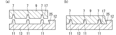
- Figures 5(a) and 5(b) are cross-sectional views showing the process of performing heat sink crimping in the first embodiment.
- Figures 20(a) and 20(b) are cross-sectional views showing the process of performing heat sink crimping in the related technology.
- the wall portion 12 is not provided (related technology)
- the outer peripheral end 17 of the first uneven portion 7 of the module base 9 (hereinafter also referred to as "end 17 of the module base 9") is not fixed even after crimping, so it is plastically deformed by the applied load, and the surface pressure on the contact portion between the end 17 of the module base 9 and the second uneven portion 11 of the heat sink base 13 is smaller than the surface pressure on other points.
- the portion adjacent to the end 17 of the module base 9 is in a state where surface pressure is applied only on one side, or is in a state where surface pressure is small on both sides, which may increase the contact thermal resistance, deteriorate the heat dissipation performance, and reduce the retention strength (vertical tensile strength).
- the wall portion 12 is provided to suppress deformation of the end portion 17 of the module base 9.
- the wall portion 12 in two places on the heat sink 2, it is possible to ensure thermal resistance and holding strength that meet the specifications without increasing the press load required to perform the heat sink crimping process.
- the relationship between the hardness of the module base 9 and the heat sink base 13 is such that the module base 9 is lower than the heat sink base 13, the above effect is even greater.
- the same effect is achieved in both cases, such as when the wall portion 12 is provided continuously so as to extend in one direction (width direction or depth direction) of the module base 9, or when a discontinuous portion is provided.
- FIGS. 6 to 8 are cross-sectional views showing the power module 202 according to a modified example of the first embodiment before integration.
- the first uneven portion 7 is composed of a plurality of recesses
- the second uneven portion 11 is composed of a plurality of protrusions.
- the second uneven part 11 of the heat sink base 13 comes into contact with the tapered part of the first uneven part 7 of the module base 9, and then slides along the tapered part to perform the heat sink crimping process.
- the heat sink crimping jig used in the heat sink crimping process can be simplified, which also improves the productivity of the heat sink crimping process.
- the height positions of the two recesses at both ends in the width direction among the multiple recesses of the first uneven portion 7 are formed to be greater than the height positions of the recesses at locations other than both ends in the width direction
- the height positions of the two protrusions at both ends in the width direction among the multiple protrusions of the second uneven portion 11 are formed to be greater than the height positions of the protrusions at locations other than both ends in the width direction.
- the provision of the wall portion 12 increases the press load required to perform the heat sink crimping process. If the required specifications are not met, it is possible to adjust the press load required to perform the heat sink crimping process by adjusting the dimensions of the wall portion 12 and the second uneven portion 11.
- a wall portion 12 is provided on the heat sink base 13, but this is not limited to this.
- the first uneven portion 7 may be composed of a plurality of convex portions
- the second uneven portion 11 may be composed of a plurality of concave portions
- the wall portion 12 protruding toward the heat sink base 13 may be provided at a position on the outer periphery side of the portion facing the second uneven portion 11 on the underside of the module base 9.
- the reference numeral 17 denotes the outer periphery end portion of the second uneven portion 11 of the heat sink base 13.
- the hardness relationship between the module base 9 and the heat sink base 13 is module base 9 > heat sink base 13.
- the width of the wall portion 12 can be increased as shown in Figure 8 to prevent the wall portion 12 from deforming.
- the same effect can be achieved whether the first uneven portion 7, the second uneven portion 11, and the wall portion 12 are provided continuously so as to extend in the depth direction, or whether discontinuous portions are provided.
- Figures 9 to 11 are cross-sectional views showing a method for manufacturing the power module 202 according to the first embodiment.
- the semiconductor chip 5 is mounted on the module base 9, and the power module section 1 is formed in which the semiconductor chip 5 is sealed by the mold section 4 while the part of the module base 9 opposite the side on which the semiconductor chip 5 is mounted is exposed.
- the heat sink 2 is prepared in which multiple heat dissipation fin insertion grooves 23a are formed.
- the power module section 1 and the heat sink base 13 are positioned so that the portion of the module base 9 exposed from the mold section 4 faces the heat sink base 13, and multiple heat dissipation fins 14 are placed in multiple heat dissipation fin insertion grooves 23a.
- the power module portion 1 is pressed toward the heat sink base 13 by a press load.
- the portion of the module base 9 exposed from the molded portion 4 is joined to the heat sink base 13, and the crimped portion of the heat sink base 13 is crimped to attach the multiple heat dissipation fins 14 to the heat sink base 13, thereby integrating the power module portion 1, the heat sink base 13, and the multiple heat dissipation fins 14.
- a crimped heat sink in which the heat dissipation fins 14 and the heat sink base 13 are integrated in advance by fin crimping.
- a heat sink 2 in which the heat sink base 13 and heat dissipation fins 14 are integrated and produced by die casting or extrusion is used instead of a crimped heat sink, it is possible to integrate the power module section 1 and the heat sink 2 by heat sink crimping using the same process and tools as in Figures 9 to 11 by using a fin crimping tool 15 with a flat tip.
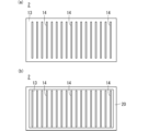
- FIGS. 12(a) and (b) are views of the heat sink 2 included in the power module 202 according to the first embodiment, viewed from below.
- FIG. 13 is a cross-sectional view showing another manufacturing method for the power module 202 according to the first embodiment.
- the press load is received by the fin crimping tool 15, but as shown in Figure 12(a), if the heat dissipation fins 14 do not extend across the depth direction of the heat sink base 13, that is, if the heat dissipation fins 14 are not arranged on the peripheral portion of the heat sink base 13, then as shown in Figure 12(b), a press load receiving portion 20 may be provided on the surface of the heat sink base 13 opposite the surface on which the second uneven portion 11 is provided, that is, on the surface on which the heat dissipation fins 14 are arranged. Specifically, the press load receiving portion 20 is provided on the peripheral portion of the lower surface of the heat sink base 13.
- the heat sink 2 is set so that the heat sink setting jig 21 abuts against the press load receiving portion 20, and then the power module portion 1 is set, making it possible to crimp the heat sink.
- the other steps are the same as those in the manufacturing method shown in Figures 9 to 11, so a description thereof will be omitted.
- the manufacturing method shown in Figure 13 is simpler and more productive than the manufacturing method shown in Figures 9 to 11.
- the power module 202 includes the module base 9, the power module section 1 having the semiconductor chip 5 mounted on one side of the module base 9 and the molded section 4 sealing the semiconductor chip 5, the heat sink base 13 integrated with the other side of the module base 9 exposed from the molded section 4, and a plurality of heat dissipation fins 14 protruding from the heat sink base 13 on the side opposite to the module base 9 and fixed to a crimping section of the heat sink base 13.
- the other side of the module base 9 is provided with a first uneven section 7, and the surface of the heat sink base 13 facing the module base 9 is provided with a second uneven section 11 that fits with the first uneven section 7 and a wall section 12 that protrudes toward the module base 9 at a position on the outer periphery side of a section facing the first uneven section 7.
- the wall portion 12 can reduce the amount of deformation of the outer peripheral end portion 17 of the first uneven portion 7, thereby suppressing an increase in contact thermal resistance and a decrease in holding strength.
- the wall portion 12 is provided not on the heat sink base 13 but on the outer periphery of the portion facing the second uneven portion 11 on the other side of the module base 9 so as to protrude toward the heat sink base 13.
- the wall portion 12 can reduce the amount of deformation at the outer peripheral end of the second uneven portion 11, thereby suppressing an increase in contact thermal resistance and a decrease in holding strength.
- first uneven portion 7, the second uneven portion 11, and the wall portion 12 may be formed to extend in the same direction, or discontinuous portions may be provided in any of the first uneven portion 7, the second uneven portion 11, and the wall portion 12. In this case as well, it is possible to suppress an increase in contact thermal resistance and a decrease in holding strength.
- a power module 202 according to a second embodiment will be described.
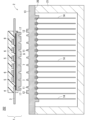
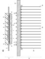
- Fig. 14 is a cross-sectional view showing the power module 202 according to the second embodiment before integration.
- Fig. 15 is a cross-sectional view of the power module 202 according to the second embodiment. Note that in the second embodiment, the same components as those described in the first embodiment are denoted by the same reference numerals, and the description thereof will be omitted.
- the heat sink base 13 has a crimping portion 22 that faces the module base 9, and a heat dissipation diffusion portion 23 on which a plurality of heat dissipation fins 14 are provided.
- the heat sink base 13 is composed of the crimping portion 22 and the heat dissipation diffusion portion 23, and by changing the thickness of the crimping portion 22, it is possible to freely design the insulation distance 28 between the lead frame 3 and the heat sink 2, specifically, between the lead frame 3 and the heat dissipation diffusion portion 23.
- the heat sink base 13 is manufactured by cutting, forging, extrusion, or die casting, so that the required insulation distance 28 can be ensured without reducing productivity.
- the heat sink base 13 is not composed of the crimped portion 22 and the heat dissipation diffusion portion 23, it is necessary to increase the thickness of the module base 9 of the power module portion 1 in order to ensure the necessary insulation distance. Increasing the thickness of the module base 9 increases the heat capacity and reduces the rate of temperature rise, which may reduce the productivity of the molding process for forming the power module portion 1.
- the first uneven portion 7 may be composed of a plurality of convex portions
- the second uneven portion 11 may be composed of a plurality of concave portions
- a wall portion 12 protruding toward the heat sink base 13 may be provided at a position on the outer periphery side of the portion of the underside of the module base 9 facing the second uneven portion 11.
- the heat sink base 13 has a crimping portion 22 that faces the module base 9 and a heat dissipation diffusion portion 23 that has a plurality of heat dissipation fins 14, and the crimping portion 22 has a second uneven portion 11 and a wall portion 12.
- the heat sink base 13 has a crimping portion 22 that faces the module base 9 and a heat dissipation diffusion portion 23 on which multiple heat dissipation fins 14 are provided, and the crimping portion 22 is provided with a second uneven portion 11.
- the heat dissipation and diffusion section 23 can diffuse heat, further improving the cooling effect and ensuring the necessary insulation distance 28 between the lead frame 3 and the heat dissipation and diffusion section 23. Furthermore, the heat dissipation and diffusion section 23 can suppress deformation of the entire heat sink base 13 that occurs during the heat sink crimping process.
- a power module 202 according to a third embodiment will be described.
- Fig. 16 is a cross-sectional view showing the power module 202 according to the third embodiment before integration.
- Fig. 17 is a cross-sectional view of the power module 202 according to the third embodiment.
- Fig. 18 is a cross-sectional view showing a process of performing heat sink caulking in the third embodiment.
- the same components as those described in the first and second embodiments are given the same reference numerals and the description thereof will be omitted.
- the wall portion 12 is formed so that its width becomes smaller as it approaches the heat sink base 13.
- the surface of the wall portion 12 that comes into contact with the end portion 17 of the module base 9 is formed in a tapered shape so that the width of the wall portion 12 becomes smaller as it approaches the heat sink base 13.
- the end portion 17 of the module base 9 will catch on the wall portion 12, making it possible to prevent a decrease in the surface pressure at the joint between the first uneven portion 7 and the second uneven portion 11 and to prevent the two from separating.
- the end 17 of the module base 9 can be crimped without increasing the press load.
- the wall portion 12 may be formed so that its width becomes smaller as it approaches the module base 9 side, as compared to FIG. 7.
- the surface of the wall portion 12 that comes into contact with the outer peripheral end of the second uneven portion 11 in the heat sink base 13 may be formed in a tapered shape so that the width of the wall portion 12 becomes smaller as it approaches the module base 9 side. This provides the same effect as in the above case.
- the same effect as in the above case can be obtained by reducing the thickness of the ends of the first uneven portion 7 and the second uneven portion 11 on the outer periphery of the recess and by increasing the width of the wall portion 12.
- the wall portion 12 is formed so that its width becomes smaller as it approaches the heat sink base 13 side. Also, the wall portion 12 is formed so that its width becomes smaller as it approaches the module base 9 side.
- the anchor effect can prevent a decrease in the surface pressure at the joint between the first uneven portion 7 and the second uneven portion 11, and prevent the two from separating.
- the power module 202 according to the above-mentioned embodiments 1 to 3 is applied to a power conversion device.
- the application of the power module 202 according to the embodiments 1 to 3 is not limited to a specific power conversion device, a case where the power module 202 according to the embodiments 1 to 3 is applied to a three-phase inverter will be described below as embodiment 4.
- FIG. 19 is a block diagram showing the configuration of a power conversion system to which the power conversion device according to this embodiment is applied.
- the power conversion system shown in FIG. 19 is composed of a power source 100, a power conversion device 200, and a load 300.
- the power source 100 is a DC power source and supplies DC power to the power conversion device 200.
- the power source 100 can be composed of various things, for example, a DC system, a solar cell, or a storage battery, or it may be composed of a rectifier circuit connected to an AC system or an AC/DC converter.
- the power source 100 may also be composed of a DC/DC converter that converts the DC power output from the DC system into a specified power.
- the power conversion device 200 is a three-phase inverter connected between the power source 100 and the load 300, converts the DC power supplied from the power source 100 into AC power, and supplies the AC power to the load 300. As shown in FIG. 19, the power conversion device 200 includes a main conversion circuit 201 that converts the DC power into AC power and outputs it, and a control circuit 203 that outputs a control signal to the main conversion circuit 201 to control the main conversion circuit 201.
- the load 300 is a three-phase motor that is driven by AC power supplied from the power conversion device 200.
- the load 300 is not limited to a specific use, but is a motor mounted on various electrical devices, and is used, for example, as a motor for hybrid cars, electric cars, railroad cars, elevators, or air conditioning equipment.
- the power conversion device 200 will be described in detail below.
- the main conversion circuit 201 includes a switching element (not shown) and a freewheeling diode (not shown), and the switching element switches to convert the DC power supplied from the power source 100 into AC power, which is then supplied to the load 300.
- the main conversion circuit 201 is a two-level three-phase full bridge circuit that can be configured with six switching elements and six freewheeling diodes connected in reverse parallel to each switching element.
- the power module 202 according to any of the above-mentioned embodiments 1 to 3 is applied to at least one of the switching elements and freewheeling diodes of the main conversion circuit 201.
- the six switching elements are connected in series with two switching elements to form upper and lower arms, and each upper and lower arm forms each phase (U phase, V phase, W phase) of the full bridge circuit.
- the output terminals of each upper and lower arm i.e., the three output terminals of the main conversion circuit 201, are connected to the load 300.
- the main conversion circuit 201 also includes a drive circuit (not shown) that drives each switching element, but the drive circuit may be built into the power module 202, or the drive circuit may be provided separately from the power module 202.
- the drive circuit generates drive signals that drive the switching elements of the main conversion circuit 201 and supplies them to the control electrodes of the switching elements of the main conversion circuit 201. Specifically, in accordance with a control signal from the control circuit 203 (described later), the drive signal that turns the switching element on and the drive signal that turns the switching element off are output to the control electrodes of each switching element.
- the drive signal When the switching element is maintained in the on state, the drive signal is a voltage signal (on signal) that is equal to or higher than the threshold voltage of the switching element, and when the switching element is maintained in the off state, the drive signal is a voltage signal (off signal) that is equal to or lower than the threshold voltage of the switching element.
- the control circuit 203 controls the switching elements of the main conversion circuit 201 so that the desired power is supplied to the load 300. Specifically, it calculates the time (on time) that each switching element of the main conversion circuit 201 should be in the on state based on the power to be supplied to the load 300.
- the main conversion circuit 201 can be controlled by PWM control, which modulates the on time of the switching elements according to the voltage to be output. Then, it outputs a control command (control signal) to a drive circuit provided in the main conversion circuit 201 so that an on signal is output to the switching element that should be in the on state at each point in time, and an off signal is output to the switching element that should be in the off state.
- the drive circuit outputs an on signal or an off signal as a drive signal to the control electrode of each switching element according to this control signal.
- the power modules 202 according to embodiments 1 to 3 are used as the switching elements and free wheel diodes of the main conversion circuit 201, thereby improving reliability.
- the power modules 202 according to the first to third embodiments are applied to a two-level three-phase inverter, but the application of the power modules 202 according to the first to third embodiments is not limited to this, and they can be applied to various power conversion devices.
- a two-level power conversion device is used, but a three-level or multi-level power conversion device may also be used, and when supplying power to a single-phase load, the power modules 202 according to the first to third embodiments may be applied to a single-phase inverter.
- the power modules 202 according to the first to third embodiments can also be applied to a DC/DC converter or an AC/DC converter.
- the power conversion device to which the power module 202 according to the first to third embodiments is applied is not limited to the case where the load described above is an electric motor, but can also be used, for example, as a power supply device for an electric discharge machine, a laser processing machine, an induction heating cooker, or a non-contact power supply system, and can also be used as a power conditioner for a solar power generation system, a power storage system, etc.
- each embodiment can be freely combined, modified, or omitted as appropriate.
- a power module section including a module base, a semiconductor element mounted on one surface side of the module base, and a mold section that seals the semiconductor element; a heat sink base integrated with the other surface of the module base exposed from the molded portion; a plurality of heat dissipation fins protruding from the heat sink base on a side opposite to the module base and fixed to a crimping portion of the heat sink base; a first concave-convex portion is provided on the other surface of the module base, a second uneven portion that fits with the first uneven portion, and a wall portion that protrudes toward the module base at a position closer to the outer periphery than a portion facing the first uneven portion.
- a power module section including a module base, a semiconductor element mounted on one surface side of the module base, and a mold section that seals the semiconductor element; a heat sink base integrated with the other surface of the module base exposed from the molded portion; a plurality of heat dissipation fins protruding from the heat sink base on a side opposite to the module base and fixed to a crimping portion of the heat sink base; a first concave-convex portion is provided on the other surface of the module base, a second concave-convex portion that fits into the first concave-convex portion is provided on a surface of the heat sink base facing the module base, a wall portion protruding toward the heat sink base at a position on the outer periphery of a portion of the other surface of the module base that faces the second uneven portion.
- the heat sink base has the crimping portion which faces the module base, and a heat dissipation diffusion portion on which a plurality of the heat dissipation fins are provided, 2.
- the crimping portion is provided with the second uneven portion and the wall portion.
- the heat sink base has the crimping portion which faces the module base, and a heat dissipation diffusion portion on which a plurality of the heat dissipation fins are provided, 3.
- (Appendix 9) a step of mounting a semiconductor element on a module base and forming a power module section in which the semiconductor element is sealed in a mold section while exposing a portion of the module base opposite to the side on which the semiconductor element is mounted; preparing a heat sink base having a plurality of heat dissipation fin insertion grooves; a step of disposing the power module unit and the heat sink base so that a portion of the module base exposed from the mold unit faces the heat sink base, and disposing a plurality of heat dissipation fins in a plurality of the heat dissipation fin insertion grooves; a step of pressing the power module section toward the heat sink base with a fin crimping tool in contact with the heat sink base to join a portion of the module base exposed from the mold section to the heat sink base, crimping the heat sink base to attach the plurality of heat dissipation fins to the heat sink base, and integrating the power module section, the heat sink base, and the plurality of heat
- (Appendix 11) a step of mounting a semiconductor element on a module base and forming a power module section in which the semiconductor element is sealed in a mold section while exposing a portion of the module base opposite to the side on which the semiconductor element is mounted; preparing a heat sink having a heat sink base and heat dissipation fins integrated therein; setting the heat sink in a heat sink setting jig; a step of positioning the power module section and the heat sink base so that a portion of the module base exposed from the molded section faces the heat sink base, and pressing the power module section toward the heat sink base to join the portion of the module base exposed from the molded section to the heat sink base;
- a method for manufacturing a power module comprising the steps of:
- a power conversion device comprising:
Landscapes
- Engineering & Computer Science (AREA)
- Power Engineering (AREA)
- Physics & Mathematics (AREA)
- Thermal Sciences (AREA)
- Microelectronics & Electronic Packaging (AREA)
- Cooling Or The Like Of Semiconductors Or Solid State Devices (AREA)
Priority Applications (1)
| Application Number | Priority Date | Filing Date | Title |
|---|---|---|---|
| JP2025520513A JPWO2024237110A1 (https=) | 2023-05-16 | 2024-05-01 |
Applications Claiming Priority (2)
| Application Number | Priority Date | Filing Date | Title |
|---|---|---|---|
| JP2023080518 | 2023-05-16 | ||
| JP2023-080518 | 2023-05-16 |
Publications (1)
| Publication Number | Publication Date |
|---|---|
| WO2024237110A1 true WO2024237110A1 (ja) | 2024-11-21 |
Family
ID=93519108
Family Applications (1)
| Application Number | Title | Priority Date | Filing Date |
|---|---|---|---|
| PCT/JP2024/016811 Ceased WO2024237110A1 (ja) | 2023-05-16 | 2024-05-01 | パワーモジュール、パワーモジュールの製造方法、および電力変換装置 |
Country Status (2)
| Country | Link |
|---|---|
| JP (1) | JPWO2024237110A1 (https=) |
| WO (1) | WO2024237110A1 (https=) |
Cited By (1)
| Publication number | Priority date | Publication date | Assignee | Title |
|---|---|---|---|---|
| CN119601549A (zh) * | 2024-11-25 | 2025-03-11 | 黑龙江汇芯半导体有限公司 | 一种半导体电路 |
Citations (5)
| Publication number | Priority date | Publication date | Assignee | Title |
|---|---|---|---|---|
| JP2014179394A (ja) * | 2013-03-14 | 2014-09-25 | Mitsubishi Electric Corp | 半導体装置 |
| JP2016086134A (ja) * | 2014-10-29 | 2016-05-19 | 三菱電機株式会社 | ヒートシンク、ヒートシンク一体型パワーモジュールおよびそれらの製造方法 |
| WO2018079396A1 (ja) * | 2016-10-31 | 2018-05-03 | 三菱電機株式会社 | 半導体装置およびその製造方法 |
| WO2018097027A1 (ja) * | 2016-11-24 | 2018-05-31 | 三菱電機株式会社 | 半導体装置およびその製造方法 |
| WO2024014410A1 (ja) * | 2022-07-14 | 2024-01-18 | 三菱電機株式会社 | パワー半導体装置および電力変換装置 |
-
2024
- 2024-05-01 JP JP2025520513A patent/JPWO2024237110A1/ja active Pending
- 2024-05-01 WO PCT/JP2024/016811 patent/WO2024237110A1/ja not_active Ceased
Patent Citations (5)
| Publication number | Priority date | Publication date | Assignee | Title |
|---|---|---|---|---|
| JP2014179394A (ja) * | 2013-03-14 | 2014-09-25 | Mitsubishi Electric Corp | 半導体装置 |
| JP2016086134A (ja) * | 2014-10-29 | 2016-05-19 | 三菱電機株式会社 | ヒートシンク、ヒートシンク一体型パワーモジュールおよびそれらの製造方法 |
| WO2018079396A1 (ja) * | 2016-10-31 | 2018-05-03 | 三菱電機株式会社 | 半導体装置およびその製造方法 |
| WO2018097027A1 (ja) * | 2016-11-24 | 2018-05-31 | 三菱電機株式会社 | 半導体装置およびその製造方法 |
| WO2024014410A1 (ja) * | 2022-07-14 | 2024-01-18 | 三菱電機株式会社 | パワー半導体装置および電力変換装置 |
Cited By (1)
| Publication number | Priority date | Publication date | Assignee | Title |
|---|---|---|---|---|
| CN119601549A (zh) * | 2024-11-25 | 2025-03-11 | 黑龙江汇芯半导体有限公司 | 一种半导体电路 |
Also Published As
| Publication number | Publication date |
|---|---|
| JPWO2024237110A1 (https=) | 2024-11-21 |
Similar Documents
| Publication | Publication Date | Title |
|---|---|---|
| US12308304B2 (en) | Semiconductor device and method of manufacturing the same, and power conversion device | |
| JP6752381B1 (ja) | 半導体モジュールおよび電力変換装置 | |
| US10971424B2 (en) | Power module and power convertor | |
| JP2021068803A (ja) | 半導体モジュール及び電力変換装置 | |
| US12477704B2 (en) | Power semiconductor device and method of manufacturing the same, and power conversion device | |
| WO2021181831A1 (ja) | 電気回路体、電力変換装置、および電気回路体の製造方法 | |
| WO2024237110A1 (ja) | パワーモジュール、パワーモジュールの製造方法、および電力変換装置 | |
| CN111211060B (zh) | 半导体装置、电力变换装置及半导体装置的制造方法 | |
| CN116171490B (zh) | 半导体装置、电力变换装置、移动体以及半导体装置的制造方法 | |
| JP7573748B2 (ja) | パワー半導体装置およびその製造方法ならびに電力変換装置 | |
| JP7766804B2 (ja) | パワー半導体装置および電力変換装置 | |
| WO2024004026A1 (ja) | 半導体装置及び電力変換装置 | |
| JP7678937B2 (ja) | パワーモジュール、パワーモジュールの製造方法、および電力変換装置 | |
| WO2022239112A1 (ja) | 半導体装置及び電力変換装置 | |
| JP2024077117A (ja) | 半導体装置、半導体装置の製造方法および電力変換装置 | |
| JP7173157B2 (ja) | 半導体装置の製造方法、半導体装置、電力変換装置、及び移動体 | |
| WO2022185545A1 (ja) | 半導体装置の製造方法、半導体装置、電力変換装置及び移動体 | |
| JP7493605B2 (ja) | 半導体モジュール、その製造方法及び電力変換装置 | |
| JP7721017B2 (ja) | 半導体装置、電力変換装置、および、半導体装置の製造方法 | |
| WO2024171848A1 (ja) | パワーモジュール、パワーモジュールの製造方法、および電力変換装置 | |
| JP2024153980A (ja) | 半導体装置及びその製造方法 | |
| JP2024106812A (ja) | 半導体装置及びその製造方法 | |
| CN119137717A (zh) | 用于制造具有翅片和外围侧壁的散热器的方法 | |
| WO2023175854A1 (ja) | 半導体装置、電力変換装置および半導体装置の製造方法 | |
| JP2022070483A (ja) | パワー半導体モジュール及びその製造方法並びに電力変換装置 |
Legal Events
| Date | Code | Title | Description |
|---|---|---|---|
| 121 | Ep: the epo has been informed by wipo that ep was designated in this application |
Ref document number: 24807064 Country of ref document: EP Kind code of ref document: A1 |
|
| WWE | Wipo information: entry into national phase |
Ref document number: 2025520513 Country of ref document: JP |
|
| NENP | Non-entry into the national phase |
Ref country code: DE |