WO2024236980A1 - 電力変換装置 - Google Patents
電力変換装置 Download PDFInfo
- Publication number
- WO2024236980A1 WO2024236980A1 PCT/JP2024/015024 JP2024015024W WO2024236980A1 WO 2024236980 A1 WO2024236980 A1 WO 2024236980A1 JP 2024015024 W JP2024015024 W JP 2024015024W WO 2024236980 A1 WO2024236980 A1 WO 2024236980A1
- Authority
- WO
- WIPO (PCT)
- Prior art keywords
- switching element
- switching
- voltage
- circuit
- gate driver
- Prior art date
- Legal status (The legal status is an assumption and is not a legal conclusion. Google has not performed a legal analysis and makes no representation as to the accuracy of the status listed.)
- Ceased
Links
Images









Classifications
-
- H—ELECTRICITY
- H02—GENERATION; CONVERSION OR DISTRIBUTION OF ELECTRIC POWER
- H02M—APPARATUS FOR CONVERSION BETWEEN AC AND AC, BETWEEN AC AND DC, OR BETWEEN DC AND DC, AND FOR USE WITH MAINS OR SIMILAR POWER SUPPLY SYSTEMS; CONVERSION OF DC OR AC INPUT POWER INTO SURGE OUTPUT POWER; CONTROL OR REGULATION THEREOF
- H02M7/00—Conversion of AC power input into DC power output; Conversion of DC power input into AC power output
- H02M7/42—Conversion of DC power input into AC power output without possibility of reversal
- H02M7/44—Conversion of DC power input into AC power output without possibility of reversal by static converters
- H02M7/48—Conversion of DC power input into AC power output without possibility of reversal by static converters using discharge tubes with control electrode or semiconductor devices with control electrode
- H02M7/483—Converters with outputs that each can have more than two voltages levels
- H02M7/487—Neutral point clamped inverters
-
- H—ELECTRICITY
- H02—GENERATION; CONVERSION OR DISTRIBUTION OF ELECTRIC POWER
- H02M—APPARATUS FOR CONVERSION BETWEEN AC AND AC, BETWEEN AC AND DC, OR BETWEEN DC AND DC, AND FOR USE WITH MAINS OR SIMILAR POWER SUPPLY SYSTEMS; CONVERSION OF DC OR AC INPUT POWER INTO SURGE OUTPUT POWER; CONTROL OR REGULATION THEREOF
- H02M1/00—Details of apparatus for conversion
- H02M1/0003—Details of control, feedback or regulation circuits
- H02M1/0006—Arrangements for supplying an adequate voltage to the control circuit of converters
-
- H—ELECTRICITY
- H03—ELECTRONIC CIRCUITRY
- H03K—PULSE TECHNIQUE
- H03K17/00—Electronic switching or gating, i.e. not by contact-making and –breaking
- H03K17/06—Modifications for ensuring a fully conducting state
- H03K17/063—Modifications for ensuring a fully conducting state in field-effect transistor switches
-
- H—ELECTRICITY
- H03—ELECTRONIC CIRCUITRY
- H03K—PULSE TECHNIQUE
- H03K2217/00—Indexing scheme related to electronic switching or gating, i.e. not by contact-making or -breaking covered by H03K17/00
- H03K2217/0081—Power supply means, e.g. to the switch driver
Definitions
- the present disclosure relates to a power conversion device, and more specifically, to a power conversion device having a bootstrap circuit.
- Patent document 1 discloses a switching element drive circuit for a three-level neutral point clamped inverter.
- the neutral point clamped inverter disclosed in Patent Document 1 includes a series circuit (switching circuit) of a first switching element, a second switching element, a third switching element, and a fourth switching element, a first clamp diode (first diode), a second clamp diode (second diode), and a series circuit (DC power supply section) of two smoothing capacitors that smooth the DC voltage and generate its neutral point potential.
- the switching element drive circuit also includes a first gate drive circuit (first gate driver) for driving the first switching element, a second gate drive circuit (second gate driver) for driving the second switching element, a third gate drive circuit (third gate driver) for driving the third switching element, and a fourth gate drive circuit (fourth gate driver) for driving the fourth switching element.
- a switching signal is input to the first gate drive circuit, the second gate drive circuit, the third gate drive circuit, and the fourth gate drive circuit by a control circuit (control unit).
- the switching element drive circuit also includes a gate power supply (power supply section).
- the negative terminal of the gate power supply is connected to the negative power supply line together with the negative terminal of the fourth gate drive circuit.
- the positive terminal of the gate power supply is connected to the positive terminal of the third gate drive circuit via a forward diode together with the positive terminal of the fourth gate drive circuit.
- the negative terminal of the third gate drive circuit is connected to the common connection point of the third switching element and the fourth switching element.
- a capacitor is connected in parallel to the third gate drive circuit.
- a voltage drop in a bootstrap circuit including a capacitor and a diode connected in parallel to the third gate drive circuit can be a problem.
- the objective of this disclosure is to provide a power conversion device that can suppress voltage drops in the bootstrap circuit.
- a power conversion device includes a DC power supply unit, a switching circuit, a first diode, a second diode, an output terminal, a first gate driver, a second gate driver, a third gate driver, a fourth gate driver, a bootstrap circuit, a power supply unit, and a control unit.
- the DC power supply unit has a positive electrode, a negative electrode, and an intermediate potential point.
- the switching circuit has a first switching element, a second switching element, a third switching element, and a fourth switching element.
- the first switching element, the second switching element, the third switching element, and the fourth switching element are connected in series between the positive electrode and the negative electrode in the order of the first switching element, the second switching element, the third switching element, and the fourth switching element from the positive electrode side.
- the cathode of the first diode is connected to a first connection point between the first switching element and the second switching element, and the anode is connected to the intermediate potential point.
- the second diode has an anode connected to a second connection point between the third switching element and the fourth switching element, and a cathode connected to the intermediate potential point.
- the output terminal is connected to a third connection point between the second switching element and the third switching element, and is connected to an AC load.
- the first gate driver drives the first switching element.
- the second gate driver drives the second switching element.
- the third gate driver drives the third switching element.
- the fourth gate driver drives the fourth switching element.
- the bootstrap circuit supplies a voltage to the third gate driver.
- the power supply unit supplies a voltage to the bootstrap circuit and the fourth gate driver.
- the control unit controls the first gate driver, the second gate driver, the third gate driver, and the fourth gate driver.
- the control unit has a first control mode, a second control mode, and a third control mode. In the first control mode, the control unit turns on the first switching element, turns on the second switching element, turns off the third switching element, and turns off the fourth switching element. In the second control mode, the control unit turns off the first switching element, turns on the second switching element, turns on the third switching element, and turns off the fourth switching element.
- the control unit turns off the first switching element, turns on the second switching element, turns off the third switching element, and turns on the fourth switching element.
- the control unit transitions to the first control mode after passing through the second control mode immediately after the third control mode.
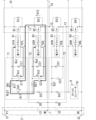
- FIG. 1 is a circuit diagram of a system including a power conversion device according to an embodiment.
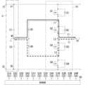
- FIG. 2 is an explanatory diagram of a current path when the switching circuit is in a first switching state (when the control unit operates in a first control mode) in the power conversion device.
- FIG. 3 is an explanatory diagram of a discharge path and a charge path when a switching circuit in the power conversion device is in a first switching state.
- FIG. 4 is an explanatory diagram of a current path when the switching circuit in the power conversion device is in a second switching state.
- FIG. 5 is an explanatory diagram of a discharge path and a charge path when a switching circuit in the power conversion device is in a second switching state.
- FIG. 6 is an explanatory diagram of a current path when the switching circuit in the power conversion device is in a third switching state.
- FIG. 7 is an explanatory diagram of a discharge path and a charge path when the switching circuit in the power conversion device is in a third switching state.
- FIG. 8 is an explanatory diagram of a current path when the switching circuit in the power conversion device is in a fourth switching state.
- FIG. 9 is an explanatory diagram of a discharge path and a charge path when a switching circuit in the power conversion device is in a fourth switching state.
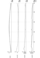
- FIG. 10 is a waveform diagram of an output current in the power conversion device of the above embodiment.
- FIG. 11 is a diagram illustrating the operation of the power conversion device.
- FIG. 12 is an operational waveform diagram of the power conversion device.
- FIG. 13 is an operational waveform diagram of the power conversion device.
- FIG. 14 is an operational waveform diagram of the power conversion device.
- FIG. 15 is an explanatory diagram of voltage command values for each phase in the power conversion device of the above embodiment.
- FIG. 16 is an explanatory diagram of a group of voltage vectors relating to the power conversion device of the above embodiment.
- FIG. 17 is a more detailed illustration of a group of voltage vectors for the power converter.
- FIG. 18 is a vector diagram for explaining the operation of the control unit in the power conversion device.
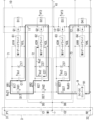
- FIG. 19 is a circuit diagram of a system including a power conversion device according to a modified example.
- a power conversion device 100 includes, for example, a DC power supply unit 3, a plurality of (for example, three) inverter circuits 1, and a control device 6, as shown in Fig. 1.
- the DC power supply unit 3 has a positive electrode P1, a negative electrode N1, and an intermediate potential point M1.
- the plurality of inverter circuits 1 are connected between the positive electrode P1 and the negative electrode N1 of the DC power supply unit 3.
- the control device 6 controls the plurality of inverter circuits 1.
- the "intermediate potential point M1" is a point that is an intermediate potential between the potential of the positive electrode P1 and the potential of the negative electrode N1 of the DC power supply unit 3.
- the power conversion device 100 is a three-level, three-phase inverter of a diode clamp type.
- each of the multiple inverter circuits 1 has an output terminal 41.
- an AC load RA1 is connected to the multiple output terminals 41.
- the AC load RA1 is, for example, a three-phase motor.
- one of the multiple inverter circuits 1 is an inverter circuit 1U that outputs a U-phase voltage
- another is an inverter circuit 1V that outputs a V-phase voltage
- the remaining one is an inverter circuit 1W that outputs a W-phase voltage.
- Each of the multiple inverter circuits 1 has a switching circuit 10, and a diode D1, a diode D2, a diode D3, and a diode D4.
- Each of the multiple inverter circuits 1 also has a diode (first diode) D5 (hereinafter also referred to as the first diode D5) and a diode D6 (hereinafter also referred to as the second diode D6).
- first diode diode
- D6 diode D6
- the potential of the intermediate potential point M1 is clamped by the first diode D5 and the second diode D6 of each inverter circuit 1.
- Each switching circuit 10 has a first switching element Q1, a second switching element Q2, a third switching element Q3, and a fourth switching element Q4.
- the first switching element Q1, the second switching element Q2, the third switching element Q3, and the fourth switching element Q4 are connected in series from the positive pole P1 side to the negative pole N1 side of the DC power supply unit 3 in the order of the first switching element Q1, the second switching element Q2, the third switching element Q3, and the fourth switching element Q4.
- the diode D1 is connected in anti-parallel to the first switching element Q1.
- the diode D2 is connected in anti-parallel to the second switching element Q2.
- the diode D3 is connected in anti-parallel to the third switching element Q3.
- the diode D4 is connected in anti-parallel to the fourth switching element Q4.
- the first diode D5 has a cathode connected to the first connection point 11 between the first switching element Q1 and the second switching element Q2, and an anode connected to the intermediate potential point M1.
- the second diode D6 has an anode connected to the second connection point 12 between the third switching element Q3 and the fourth switching element Q4, and a cathode connected to the intermediate potential point M1.
- the control device 6 has a plurality of (e.g., three) first gate drivers 61, a plurality of (e.g., three) second gate drivers 62, a plurality of (e.g., three) third gate drivers 63, and a plurality of (e.g., three) fourth gate drivers 64.
- the control device 6 also has a plurality of (e.g., three) first bootstrap circuits 71, a plurality of (e.g., three) second bootstrap circuits 72, a plurality of (e.g., three) third bootstrap circuits 73, a power supply unit 9, and a control unit 60.
- the multiple first gate drivers 61 drive the first switching element Q1 of each of the multiple inverter circuits 1.
- the multiple second gate drivers 62 drive the second switching element Q2 of each of the multiple inverter circuits 1.
- the multiple third gate drivers 63 drive the third switching element Q3 of each of the multiple inverter circuits 1.
- the multiple fourth gate drivers 64 drive the fourth switching element Q4 of each of the multiple inverter circuits 1.
- the multiple first bootstrap circuits 71 correspond one-to-one to the multiple first gate drivers 61. Each of the multiple first bootstrap circuits 71 supplies a voltage to the corresponding first gate driver 61.
- the multiple second bootstrap circuits 72 correspond one-to-one to the multiple second gate drivers 62. Each of the multiple second bootstrap circuits 72 supplies a voltage to the corresponding second gate driver 62.
- the multiple third bootstrap circuits 73 correspond one-to-one to the multiple third gate drivers 63. Each of the multiple third bootstrap circuits 73 supplies a voltage to the corresponding third gate driver 63.
- the power supply unit 9 supplies a voltage to the multiple fourth gate drivers 64.
- the control unit 60 controls a plurality of first gate drivers 61, a plurality of second gate drivers 62, a plurality of third gate drivers 63, and a plurality of fourth gate drivers 64.
- the DC power supply unit 3 has a first capacitor C1 and a second capacitor C2. In the DC power supply unit 3, the first capacitor C1 and the second capacitor C2 are connected in series. The DC power supply unit 3 further has a first DC terminal 31 connected to the positive pole P1 and a second DC terminal 32 connected to the negative pole N1. In the DC power supply unit 3, a first end of the first capacitor C1 is connected to the first DC terminal 31, a second end of the first capacitor C1 is connected to the first end of the second capacitor C2, and a second end of the second capacitor C2 is connected to the second DC terminal 32. In the DC power supply unit 3, a connection point between the first capacitor C1 and the second capacitor C2 is an intermediate potential point M1.
- a DC voltage source E1 is connected between the first DC terminal 31 and the second DC terminal 32.
- the output voltage Vdc of the DC voltage source E1 is applied between the positive electrode P1 and the negative electrode N1 of the DC power supply unit 3.
- the capacitance of the second capacitor C2 is the same as the capacitance of the first capacitor C1.
- the capacitance of the second capacitor C2 is the same as the capacitance of the first capacitor C1
- the switching circuit 10 included in inverter circuit 1U may be referred to as switching circuit 10U
- the switching circuit 10 included in inverter circuit 1V may be referred to as switching circuit 10V
- the switching circuit 10 included in inverter circuit 1W may be referred to as switching circuit 10W
- the output terminal 41 included in inverter circuit 1U may be referred to as output terminal 41U
- the output terminal 41 included in inverter circuit 1V may be referred to as output terminal 41V
- the output terminal 41 included in inverter circuit 1W may be referred to as output terminal 41W.
- the first switching element Q1, the second switching element Q2, the third switching element Q3, and the fourth switching element Q4 of each switching circuit 10 have a control terminal, a first main terminal, and a second main terminal.
- the first switching element Q1, the second switching element Q2, the third switching element Q3, and the fourth switching element Q4 of each switching circuit 10 are, for example, MOSFETs. Therefore, the control terminal, the first main terminal, and the second main terminal of each of the first switching element Q1, the second switching element Q2, the third switching element Q3, and the fourth switching element Q4 of each switching circuit 10 are the gate terminal, the drain terminal, and the source terminal, respectively.
- the MOSFETs constituting each of the first switching element Q1, the second switching element Q2, the third switching element Q3, and the fourth switching element Q4 are, for example, normally-off type n-channel MOSFETs.
- the MOSFETs are Si-based MOSFETs, but are not limited to Si-based MOSFETs and may be, for example, SiC-based MOSFETs.
- the control terminal of the first switching element Q1 of each switching circuit 10 is connected to a corresponding first gate driver 61 of the multiple first gate drivers 61.
- the control terminal of the second switching element Q2 of each switching circuit 10 is connected to a corresponding second gate driver 62 of the multiple second gate drivers 62.
- the control terminal of the third switching element Q3 of each switching circuit 10 is connected to a corresponding third gate driver 63 of the multiple third gate drivers 63.
- the control terminal of the fourth switching element Q4 of each switching circuit 10 is connected to a corresponding fourth gate driver 64 of the multiple fourth gate drivers 64.
- the first main terminal of the first switching element Q1 is connected to the positive pole P1 of the DC power supply unit 3, and the second main terminal of the first switching element Q1 is connected to the first main terminal of the second switching element Q2. Also, in each switching circuit 10, the second main terminal of the second switching element Q2 is connected to the first main terminal of the third switching element Q3. Also, in each switching circuit 10, the second main terminal of the third switching element Q3 is connected to the first main terminal of the fourth switching element Q4, and the second main terminal of the fourth switching element Q4 is connected to the negative pole N1 of the DC power supply unit 3.
- the third connection point 13 between the second switching element Q2 and the third switching element Q3 in the switching circuit 10U is connected to the output terminal 41U.
- the third connection point 13 between the second switching element Q2 and the third switching element Q3 in the switching circuit 10V is connected to the output terminal 41V.
- the third connection point 13 between the second switching element Q2 and the third switching element Q3 in the switching circuit 10W is connected to the output terminal 41W.
- the third connection point 13 of the inverter circuit 1U is connected to, for example, the U phase of the AC load RA1 via the output terminal 41U.
- the third connection point 13 of the inverter circuit 1V is connected to, for example, the V phase of the AC load RA1 via the output terminal 41V.
- the third connection point 13 of the inverter circuit 1W is connected to, for example, the W phase of the AC load RA1 via the output terminal 41W.
- the anode of the diode D1 is connected to the second main terminal (source terminal) of the first switching element Q1, and the cathode of the diode D1 is connected to the first main terminal (drain terminal) of the first switching element Q1.
- the anode of the diode D2 is connected to the second main terminal (source terminal) of the second switching element Q2, and the cathode of the diode D2 is connected to the first main terminal (drain terminal) of the second switching element Q2.
- the anode of the diode D3 is connected to the second main terminal (source terminal) of the third switching element Q3, and the cathode of the diode D3 is connected to the first main terminal (drain terminal) of the third switching element Q3.
- the anode of the diode D4 is connected to the second main terminal (source terminal) of the fourth switching element Q4, and the cathode of the diode D4 is connected to the first main terminal (drain terminal) of the fourth switching element Q4.
- the diode D1 may be replaced by a parasitic diode of the MOSFET that constitutes the first switching element Q1.
- the diode D2 may be replaced by a parasitic diode of the MOSFET that constitutes the second switching element Q2.
- the diode D3 may be replaced by a parasitic diode of the MOSFET that constitutes the third switching element Q3.
- the diode D4 may be replaced by a parasitic diode of the MOSFET that constitutes the fourth switching element Q4.
- the cathode of the first diode D5 is connected to the first connection point 11 between the first switching element Q1 and the second switching element Q2.
- the anode of the first diode D5 is connected to the intermediate potential point M1 of the DC power supply unit 3.
- the intermediate potential point M1 is connected to ground, the potential of the intermediate potential point M1 is 0V.
- the potential of the positive electrode P1 is Vdc/2
- the potential of the negative electrode N1 is -Vdc/2.
- the cathode of the second diode D6 is connected to the intermediate potential point M1.
- the anode of the second diode D6 is connected to the second connection point 12 between the third switching element Q3 and the fourth switching element Q4.
- the multiple first gate drivers 61 correspond one-to-one to the multiple first switching elements Q1. Each of the multiple first gate drivers 61 is connected to a control terminal of the corresponding first switching element Q1. Each of the multiple first gate drivers 61 drives the corresponding first switching element Q1.
- the multiple first gate drivers 61 are connected to the control unit 60.
- the control unit 60 outputs multiple first control signals S1 (see FIG. 2) that correspond one-to-one to the multiple first gate drivers 61.
- Each of the multiple first gate drivers 61 controls the on/off of the first switching element Q1 based on the given first control signal S1.
- the second gate drivers 62 correspond one-to-one to the second switching elements Q2. Each of the second gate drivers 62 is connected to a control terminal of the corresponding second switching element Q2. Each of the second gate drivers 62 drives the corresponding second switching element Q2.
- the second gate drivers 62 are connected to the control unit 60.
- the control unit 60 outputs second control signals S2 (see FIG. 2) that correspond one-to-one to the second gate drivers 62.
- Each of the second gate drivers 62 controls the on/off of the second switching element Q2 based on the second control signal S2 provided.
- the multiple third gate drivers 63 correspond one-to-one to the multiple third switching elements Q3. Each of the multiple third gate drivers 63 is connected to the control terminal of the corresponding third switching element Q3. Each of the multiple third gate drivers 63 drives the corresponding third switching element Q3.
- the multiple third gate drivers 63 are connected to the control unit 60.
- the control unit 60 outputs multiple third control signals S3 (see FIG. 2) that correspond one-to-one to the multiple third gate drivers 63.
- Each of the multiple third gate drivers 63 controls the on/off of the third switching element Q3 based on the provided third control signal S3.
- the multiple fourth gate drivers 64 correspond one-to-one to the multiple fourth switching elements Q4. Each of the multiple fourth gate drivers 64 is connected to the control terminal of the corresponding fourth switching element Q4. Each of the multiple fourth gate drivers 64 drives the corresponding fourth switching element Q4.
- the multiple fourth gate drivers 64 are connected to the control unit 60.
- the control unit 60 outputs multiple fourth control signals S4 (see FIG. 2) that correspond one-to-one to the multiple fourth gate drivers 64.
- Each of the multiple fourth gate drivers 64 controls the on/off of the fourth switching element Q4 based on the provided fourth control signal S4.
- the first bootstrap circuits 71 correspond one-to-one to the first gate drivers 61.
- the first bootstrap circuits 71 supply voltages to the corresponding first gate drivers 61.
- Each of the first bootstrap circuits 71 has a diode D17, a resistor R17, and a capacitor C17 (also called a boost capacitor C17).
- the anode of the diode D17 is connected to the positive terminal of the power supply unit 9 via the diode D27 and the diode D37, and the cathode of the diode D17 is connected to the first end of the capacitor C17 via the resistor R17.
- the first end of the capacitor C17 is connected to the high-potential power supply terminal 61H (see FIG.
- the first bootstrap circuit 71 supplies the first gate driver 61 with a voltage required to turn on the first switching element Q1 in the first gate driver 61.
- Each of the first bootstrap circuits 71 further includes a Zener diode Z17 connected in parallel to the capacitor C17.
- the second bootstrap circuits 72 correspond one-to-one to the second gate drivers 62.
- the second bootstrap circuits 72 supply voltages to the corresponding second gate drivers 62.
- Each of the second bootstrap circuits 72 has a diode D27, a resistor R27, and a capacitor C27 (also called a boost capacitor C27).
- the anode of the diode D27 is connected to the positive terminal of the power supply unit 9 via a diode D37, and the cathode of the diode D27 is connected to a first end of the capacitor C27 via a resistor R27.
- the first end of the capacitor C27 is connected to the high potential side power supply terminal 62H (see FIG.
- the second bootstrap circuit 72 supplies the second gate driver 62 with a voltage required to turn on the second switching element Q2 in the second gate driver 62.
- Each of the second bootstrap circuits 72 further includes a Zener diode Z27 connected in parallel to the capacitor C27.
- the third bootstrap circuits 73 correspond one-to-one to the third gate drivers 63.
- the third bootstrap circuits 73 supply voltages to the corresponding third gate drivers 63.
- Each of the third bootstrap circuits 73 includes a diode D37, a resistor R37, and a capacitor C37 (also called a boost capacitor C37).
- the anode of the diode D37 is connected to the positive terminal of the power supply unit 9, and the cathode of the diode D37 is connected to a first end of the capacitor C37 via the resistor R37.
- the first end of the capacitor C37 is connected to the high-potential power supply terminal 63H (see FIG.
- the third bootstrap circuit 73 supplies the third gate driver 63 with a voltage required to turn on the third switching element Q3 in the third gate driver 63.
- Each of the multiple third bootstrap circuits 73 further includes a Zener diode Z37 connected in parallel to the capacitor C37.
- the power supply unit 9 supplies voltage to the multiple (three) first bootstrap circuits 71, the multiple (three) second bootstrap circuits 72, the multiple (three) third bootstrap circuits 73, and the multiple (three) fourth gate drivers 64.
- the power supply unit 9 is, for example, a DC power supply including an isolated DC-DC converter 91.
- the positive terminal of the power supply unit 9 is connected to the high potential power supply terminal 64H (see FIG. 3) of each of the multiple fourth gate drivers 64, and the negative terminal of the power supply unit 9 is connected to the low potential power supply terminal 64L (see FIG. 3) of each of the multiple fourth gate drivers 64.
- the control unit 60 controls a plurality of first gate drivers 61, a plurality of second gate drivers 62, a plurality of third gate drivers 63, and a plurality of fourth gate drivers 64.
- the control unit 60 controls a plurality of first switching elements Q1, a plurality of second switching elements Q2, a plurality of third switching elements Q3, and a plurality of fourth switching elements Q4.
- the execution subject of the control unit 60 includes a computer system.
- the computer system has one or more computers.
- the computer system is mainly composed of a processor and a memory as hardware.
- the processor executes a program recorded in the memory of the computer system, thereby realizing the function of the control unit 60 as the execution subject in this disclosure.
- the program may be pre-recorded in the memory of the computer system, or may be provided through an electric communication line, or may be recorded and provided on a non-transitory recording medium such as a memory card, an optical disk, or a hard disk drive (magnetic disk) that can be read by the computer system.
- the processor of the computer system is composed of one or more electronic circuits including a semiconductor integrated circuit (IC) or a large-scale integrated circuit (LSI).
- the multiple electronic circuits may be integrated into one chip, or may be distributed across multiple chips.
- the multiple chips may be integrated into one device, or may be distributed across multiple devices.
- the control unit 60 outputs a plurality (three) of first control signals S1 (see FIG. 2) for controlling a plurality (three) of first switching elements Q1, a plurality (three) of second control signals S2 (see FIG. 2) for controlling a plurality (three) of second switching elements Q2, a plurality (three) of third control signals S3 (see FIG. 2) for controlling a plurality of third switching elements Q3, and a plurality (three) of fourth control signals S4 for controlling a plurality (three) of fourth switching elements Q4.
- FIG. 2 shows only one inverter circuit 1 of the three inverter circuits 1 (see FIG. 1), and the remaining two inverter circuits 1 are not shown.
- the first gate drivers 61, the second gate drivers 62, the third gate drivers 63, the fourth gate drivers 64, the first bootstrap circuits 71, the second bootstrap circuits 72, the third bootstrap circuits 73, and the power supply unit 9 shown in FIG. 1 are omitted.
- FIG. 3 only one inverter circuit 1 of the three inverter circuits 1 (see FIG. 1) is shown, and the remaining two inverter circuits 1 are omitted.
- the two first gate drivers 61, the two second gate drivers 62, the two third gate drivers 63, the two fourth gate drivers 64, the two first bootstrap circuits 71, the two second bootstrap circuits 72, and the two third bootstrap circuits 73 shown in FIG. 1 are omitted.
- the three first control signals S1 include a first control signal S1U that controls the first switching element Q1 of the switching circuit 10U, a first control signal S1V that controls the first switching element Q1 of the switching circuit 10V, and a first control signal S1W that controls the first switching element Q1 of the switching circuit 10W.
- the three second control signals S2 include a second control signal S2U that controls the second switching element Q2 of the switching circuit 10U, a second control signal S2V that controls the second switching element Q2 of the switching circuit 10V, and a second control signal S2W that controls the second switching element Q2 of the switching circuit 10W.
- the three third control signals S3 include a third control signal S3U that controls the third switching element Q3 of the switching circuit 10U, a third control signal S3V that controls the third switching element Q3 of the switching circuit 10V, and a third control signal S3W that controls the third switching element Q3 of the switching circuit 10W.
- the three fourth control signals S4 include a fourth control signal S4U that controls the fourth switching element Q4 of the switching circuit 10U, a fourth control signal S4V that controls the fourth switching element Q4 of the switching circuit 10V, and a fourth control signal S4W that controls the fourth switching element Q4 of the switching circuit 10W.
- Each of the multiple first control signals S1, multiple second control signals S2, multiple third control signals S3, and multiple fourth control signals S4 is, for example, a signal whose potential level changes between a first potential level (hereinafter also referred to as a low level) and a second potential level (hereinafter also referred to as a high level) that is higher than the first potential level.
- the first potential level is, for example, 0V
- the second potential level is a potential level greater than the gate threshold voltage of the MOSFET. That is, for each of the multiple control signals (multiple first control signals S1, multiple second control signals S2, multiple third control signals S3, and multiple fourth control signals S4), the first potential level is a potential level for turning off the switching element corresponding to that control signal, and the second potential level is a potential level for turning on the switching element corresponding to that control signal.
- Each of the multiple first switching elements Q1 is turned on when the corresponding first control signal S1 is at a high level, and turned off when it is at a low level.
- Each of the multiple second switching elements Q2 is turned on when the corresponding second control signal S2 is at a high level, and turned off when it is at a low level.
- Each of the multiple third switching elements Q3 is turned on when the corresponding third control signal S3 is at a high level, and turned off when it is at a low level.
- Each of the multiple fourth switching elements Q4 is turned on when the corresponding fourth control signal S4 is at a high level, and turned off when it is at a low level.
- each of the multiple inverter circuits 1 is controlled to a first switching state or a second switching state, a third switching state or a fourth switching state. That is, in the power conversion device 100, the switching state of the switching circuit 10 in each of the three inverter circuits 1U, 1V, 1W is controlled to any one of a first switching state, a second switching state, a third switching state, and a fourth switching state.
- the first switching state, the second switching state, the third switching state, and the fourth switching state have different combinations of on/off states of the first to fourth switching elements Q1 to Q4.
- the output voltage in the first switching state, the output voltage in the second switching state, and the output voltage in the third switching state are different from one another. That is, in each of the multiple inverter circuits 1, the potential level of the output voltage changes in three levels depending on the states of the first to fourth switching elements Q1 to Q4. Regarding the output voltages of the multiple inverter circuits 1, the output voltage of the U-phase inverter circuit 1U, the output voltage of the V-phase inverter circuit 1V, and the output voltage of the W-phase inverter circuit 1W are out of phase with each other.
- the first switching state is a combination in which both the first switching element Q1 and the second switching element Q2 are in the on state, and both the third switching element Q3 and the fourth switching element Q4 are in the off state.
- each of the multiple inverter circuits 1 can output an output voltage at the potential level of the positive electrode P1 of the DC power supply unit 3.
- each of the multiple inverter circuits 1 has the potential of the third connection point 13 at the potential level of the positive electrode P1 of the DC power supply unit 3 (e.g., Vdc/2).
- the second switching state is a combination in which both the first switching element Q1 and the fourth switching element Q4 are in the off state, and both the second switching element Q2 and the third switching element Q3 are in the on state.
- each of the multiple inverter circuits 1 can output an output voltage at the potential level of the intermediate potential point M1 of the DC power supply unit 3.
- the potential of the third connection point 13 becomes the potential level of the intermediate potential point M1 (e.g., 0).
- the third switching state is a combination in which both the first switching element Q1 and the second switching element Q2 are in the off state, and both the third switching element Q3 and the fourth switching element Q4 are in the on state.
- each of the multiple inverter circuits 1 can output an output voltage at the potential level of the negative electrode N1 of the DC power supply unit 3.
- each of the multiple inverter circuits 1 has the potential of the third connection point 13 at the potential level of the negative electrode N1 of the DC power supply unit 3 (for example, -Vdc/2).
- the fourth switching state is a combination in which both the second switching element Q2 and the fourth switching element Q4 are in the on state, and both the first switching element Q1 and the third switching element Q3 are in the off state.
- each of the multiple inverter circuits 1 can output an output voltage at the potential level of the intermediate potential point M1 of the DC power supply unit 3.
- each of the multiple inverter circuits 1 has the potential of the third connection point 13 at the potential level of the intermediate potential point M1 (e.g., 0).
- the switching circuit 10 of the inverter circuit 1 when the switching circuit 10 of the inverter circuit 1 is in the first switching state, the voltage required for the first gate driver 61 to turn on the first switching element Q1 is supplied from the capacitor C17 of the first bootstrap circuit 71 to the first gate driver 61. Therefore, as shown in FIG. 3, the charge in the capacitor C17 of the first bootstrap circuit 71 is discharged through a discharge path Ru1 that is capacitor C17-high potential side power supply terminal 61H of the first gate driver 61-low potential side power supply terminal 61L of the first gate driver 61-capacitor C17. As a result, in the first bootstrap circuit 71, the voltage across the capacitor C17 decreases over time.
- the switching circuit 10 of the inverter circuit 1 when the switching circuit 10 of the inverter circuit 1 is in the first switching state, the voltage required for the second gate driver 62 to turn on the second switching element Q2 is supplied from the capacitor C27 of the second bootstrap circuit 72 to the second gate driver 62. Therefore, the charge in the capacitor C27 of the second bootstrap circuit 72 is discharged via the discharge path Ru2 from the capacitor C27 to the high potential side power supply terminal 62H of the second gate driver 62 to the low potential side power supply terminal 62L of the second gate driver 62 to the capacitor C27. As a result, in the second bootstrap circuit 72, the voltage across the capacitor C27 decreases over time.
- the capacitor C17 is charged by the capacitor C27 if the first condition is satisfied. As shown in FIG. 3, if the voltage across the capacitor C17 is Vo1, the voltage across the capacitor C27 is Vo2, the voltage across the diode D17 is Vd1, the voltage across the resistor R17 is VR1, and the voltage across the second switching element Q2 is Vf2, the first condition is Vo2>(Vo1+Vd1+VR1+Vf2).
- the charging path Ru21 that charges the capacitor C17 by the capacitor C27 is the path of the capacitor C27-resistor R27-diode D17-resistor R17-capacitor C17-first connection point 11-second switching element Q2-capacitor C27.
- the current I1 flows through the path of the intermediate potential point M1 of the DC power supply unit 3 - the first diode D5 of the inverter circuit 1U - the second switching element Q2 of the switching circuit 10U - the third connection point 13 - the output terminal 41.
- the switching circuit 10 of the inverter circuit 1 when the switching circuit 10 of the inverter circuit 1 is in the second switching state and the polarity of the output current is negative, as shown in FIG. 4, the current I1 flows through the path of the output terminal 41-the third connection point 13-the third switching element Q3-the second connection point 12-the second diode D6 (path indicated by the thick dashed arrow), and the voltage value of the output voltage to the AC load RA1 becomes 0.
- the switching circuits 10U, 10V, and 10W are in the second switching state, the second switching state, and the first switching state, respectively, in the inverter circuit 1U, the current I1 flows through the path of the output terminal 41-the third connection point 13-the third switching element Q3-the second connection point 12-the second diode D6 (path indicated by the thick dashed arrow), and the voltage value of the output voltage to the AC load RA1 becomes 0.
- the switching circuit 10 of the inverter circuit 1 When the switching circuit 10 of the inverter circuit 1 is in the second switching state, the voltage required to turn on the second switching element Q2 is supplied from the capacitor C27 of the second bootstrap circuit 72 to the second gate driver 62 by the second gate driver 62. Therefore, the charge of the capacitor C27 of the second bootstrap circuit 72 is discharged through a discharge path Ru2 of the capacitor C27-the high potential side power supply terminal 62H of the second gate driver 62-the low potential side power supply terminal 62L of the second gate driver 62-the capacitor C27, as shown in FIG. 5.
- the switching circuit 10 of the inverter circuit 1 When the switching circuit 10 of the inverter circuit 1 is in the second switching state, the voltage required to turn on the third switching element Q3 is supplied from the capacitor C37 of the third bootstrap circuit 73 to the third gate driver 63 by the third gate driver 63. Therefore, the charge in the capacitor C37 of the third bootstrap circuit 73 is discharged through the discharge path Ru3 from the capacitor C37 to the high potential side power supply terminal 63H of the third gate driver 63 to the low potential side power supply terminal 63L of the third gate driver 63 to the capacitor C37.
- the capacitor C27 is charged by the capacitor C37 if the second condition is met, and the capacitor C17 is charged by the capacitor C27 if the third condition is met.
- the voltages across the capacitors C17, C27, and C37 are Vo1, Vo2, and Vo3, respectively, the voltages across the diodes D17 and D27 are Vd1 and Vd2, respectively, the voltages across the resistors R17 and R27 are VR1 and VR2, respectively, and the voltages across the second switching element Q2 and the third switching element Q3 are Vf2 and Vf3, respectively, the second condition is Vo3>(Vo2+Vd2+VR2+Vf3).
- the third condition is Vo2>(Vo1+Vd1+VR1+Vf2).
- the charging path Ru32 that charges the capacitor C27 with the capacitor C37 is the path of the capacitor C37-resistor R37-diode D27-resistor R27-capacitor C27-third connection point 13-third switching element Q3-capacitor C37.
- the charging path Ru21 that charges the capacitor C17 with the capacitor C27 is the path of the capacitor C27-resistor R27-diode D17-resistor R17-capacitor C17-first connection point 11-second switching element Q2-capacitor C27.
- the capacitor C37 of the third bootstrap circuit 73 supplies the third gate driver 63 with the voltage required to turn on the third switching element Q3 by the third gate driver 63. 7, the charge of capacitor C37 of the third bootstrap circuit 73 is discharged through a discharge path Ru3 that is capacitor C37-high potential side power supply terminal 63H of the third gate driver 63-low potential side power supply terminal 63L of the third gate driver 63-capacitor C37. Furthermore, when the switching circuit 10 of the inverter circuit 1 is in the third switching state, capacitor C37 is charged by the power supply unit 9 if a fourth condition is satisfied, and capacitor C27 is charged by capacitor C37 if a fifth condition is satisfied.
- the voltage across the power supply unit 9 is Voo
- the voltage across the capacitors C27 and C37 is Vo2 and Vo3
- the voltage across the diodes D27 and D37 is Vd2 and Vd3
- the voltage across the resistors R27 and R37 is VR2 and VR3
- the voltage across the third switching element Q3 and the fourth switching element Q4 is Vf3 and Vf4.
- the fourth condition is Voo>(Vo3+Vd3+VR3+Vf4).
- the fifth condition is Vo3>(Vo2+Vd2+VR2+Vf3).
- the charging path Ru93 for charging the capacitor C37 by the power supply unit 9 is a path from the positive terminal of the power supply unit 9 to the diode D37, the resistor R37, the capacitor C37, the second connection point 12, the fourth switching element Q4, and the negative terminal of the power supply unit 9.
- the charging path Ru32, which charges the capacitor C27 using the capacitor C37, is the path of the capacitor C37 - resistor R37 - diode D27 - resistor R27 - capacitor C27 - third connection point 13 - third switching element Q3 - capacitor C37.
- the capacitor C27 of the second bootstrap circuit 72 supplies the second gate driver 62 with a voltage required to turn on the second switching element Q2 by the second gate driver 62. Therefore, as shown in FIG. 9, the charge of the capacitor C27 of the second bootstrap circuit 72 is discharged through a discharge path Ru2 of the capacitor C27-the high potential side power supply terminal 62H of the second gate driver 62-the low potential side power supply terminal 62L of the second gate driver 62-the capacitor C27.
- the power supply unit 9 supplies the fourth gate driver 64 with a voltage required to turn on the fourth switching element Q4 by the fourth gate driver 64.
- the capacitor C37 is charged by the power supply unit 9.
- the charging path Ru93 through which the power supply unit 9 charges the capacitor C37 is a path from the positive terminal of the power supply unit 9 to the diode D37 to the resistor R37 to the capacitor C37 to the second connection point 12 to the fourth switching element Q4 to the negative terminal of the power supply unit 9.
- the control unit 60 has a first control mode, a second control mode, and a third control mode.
- the control unit 60 turns on the first switching element Q1, turns on the second switching element Q2, turns off the third switching element Q3, and turns off the fourth switching element Q4. More specifically, in the first control mode, the control unit 60 controls the first switching element Q1, the second switching element Q2, the third switching element Q3, and the fourth switching element Q4 so that the switching circuit 10 is in the first switching state.
- the control unit 60 turns off the first switching element Q1, turns on the second switching element Q2, turns on the third switching element Q3, and turns off the fourth switching element Q4. More specifically, in the second control mode, the control unit 60 controls the first switching element Q1, the second switching element Q2, the third switching element Q3, and the fourth switching element Q4 so that the switching circuit 10 is in the second switching state.
- the control unit 60 turns off the first switching element Q1, turns on the second switching element Q2, turns off the third switching element Q3, and turns on the fourth switching element Q4. More specifically, in the third control mode, the control unit 60 controls the first switching element Q1, the second switching element Q2, the third switching element Q3, and the fourth switching element Q4 so that the switching circuit 10 is in the fourth switching state.
- the waveform of the output current will be sinusoidal, for example, as shown in FIG. 10.
- the output current of the U phase, the output current of the V phase, and the output current of the W phase are sinusoidal currents that are, for example, 120° out of phase with each other.
- the control unit 60 When the polarity of the current flowing through the output terminal 41 is positive, the control unit 60 alternates between the first control mode and the second control mode.
- the control unit 60 when transitioning from the first control mode to the second control mode, the control unit 60 performs control in the third control mode between the first control mode and the second control mode. Therefore, immediately after the third control mode, the control unit 60 transitions through the second control mode and then to the first control mode.
- a low level is indicated as "L” and a high level is indicated as "H”.
- the control unit 60 also sets a dead time period Td between the period when the potential level of the control signal S4 is high and the period when the potential level of the control signal S3 is high, so that the on period of the fourth switching element Q4 and the on period of the third switching element Q3 do not overlap.
- the control unit 60 also sets a dead time period Td between the period when the potential level of the control signal S1 is high and the period when the potential level of the control signal S4 is high, so that the on period of the first switching element Q1 and the on period of the fourth switching element Q4 do not overlap.
- the control unit 60 also sets a dead time period Td between the period when the potential level of the control signal S3 is high and the period when the potential level of the control signal S1 is high, so that the on period of the third switching element Q3 and the on period of the first switching element Q1 do not overlap.
- the length of the dead time period Td may be 0.
- the control unit 60 sets the length T4 of the on-period of the fourth switching element Q4 in the third control mode to be 90% or more and 110% or less of the CR time constant of the third bootstrap circuit 73 that supplies a voltage to the third gate driver 63.
- the CR time constant of the third bootstrap circuit 73 is determined by the capacitance of the capacitor C37 and the resistance value of the resistor R37 of the third bootstrap circuit 73.
- the control unit 60 also has a fourth control mode.
- the control unit 60 turns off the first switching element Q1, turns off the second switching element Q2, turns on the third switching element Q3, and turns on the fourth switching element Q4. More specifically, in the fourth control mode, the control unit 60 controls the first switching element Q1, the second switching element Q2, the third switching element Q3, and the fourth switching element Q4 so that the switching circuit 10 is in the third switching state.
- control unit 60 When the polarity of the output current (current I1) flowing through the output terminal 41 is negative, the control unit 60 alternates between the second control mode and the fourth control mode.
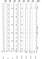
- Figure 12 shows the waveforms of current I1, voltage Vo1 across capacitor C17, voltage Vo2 across capacitor C27, and voltage Vo3 across capacitor C37 during the period when the polarity of the output current flowing through output terminal 41 is positive in the embodiment.
- Figure 12 shows an example in which the switching frequency is set to 20 kHz and the frequency of the output current (current I1) is set to 50 Hz.
- Figure 12 also shows an example in which the length of the dead time period Td is set to 0.
- FIG. 13 shows the waveforms of current I1, control signal S3, control signal S4, voltage VQ3 across third switching element Q3, voltage VQ4 across fourth switching element Q4, voltage Vo1 across capacitor C17, voltage Vo2 across capacitor C27, and voltage Vo3 across capacitor C37 for a portion of the period during which the polarity of the output current flowing through output terminal 41 is positive in the above embodiment.
- the period between time t1 and time t2 is the period during which the control mode of the control unit 60 is the second control mode.
- the period between time t2 and time t3 is the period during which the control mode of the control unit 60 is the first control mode.
- the period between time t3 and time t4 is the period during which the control mode of the control unit 60 is the third control mode.
- the period between time t4 and time t5 is the period during which the control mode of the control unit 60 is the second control mode.
- the control unit 60 does not have the third control mode, and alternates between the first control mode and the second control mode described above during the period when the output current is positive.
- "A0" is the waveform of the current I1 in the above embodiment.
- the current I1 in the comparative example is not shown because it does not decrease from the current I1 in the above embodiment and overlaps with "A0".
- the control unit 60 employs voltage vector control as its control method.
- the voltage vector control performed by the control unit 60 will be explained below with reference to Figures 15 to 18.
- the control unit 60 generates the first to fourth control signals S1U to S4U, the first to fourth control signals S1V to S4V, and the first to fourth control signals S1W to S4W based on the voltage commands Vu, Vv, and Vw (see FIG. 15) related to the output voltages of the inverter circuits 1U, 1V, and 1W, respectively.
- the first to fourth control signals S1U to S4U are the first to fourth control signals S1 to S4 for the first to fourth switching elements Q1 to Q4 of the inverter circuit 1U.
- the first to fourth control signals S1V to S4V are the first to fourth control signals S1 to S4 for the first to fourth switching elements Q1 to Q4 of the inverter circuit 1V.
- the first to fourth control signals S1W to S4W are the first to fourth control signals S1 to S4 for the first to fourth switching elements Q1 to Q4 of the inverter circuit 1W.
- the voltage command Vu, the voltage command Vv, and the voltage command Vw are sinusoidal signals, for example, with a phase difference of 120°, and each of the voltage commands changes in value (voltage command value) over time.
- the length of one period of each of the voltage command Vu, the voltage command Vv, and the voltage command Vw is the same.
- the control unit 60 may perform PI (Proportional Integral) control of the voltage commands Vu, Vv, and Vw based on information output from a detection unit 8 (see FIG. 1) that detects the state of the AC load RA1.
- PI Proportional Integral
- the information output from the detection unit 8 includes, for example, at least one of the following: information on the detection results of a plurality of current sensors that detect the output currents flowing through the U-phase, V-phase, and W-phase of the AC load RA1; and information on the detection results of an encoder that detects the rotation speed, rotation angle, etc. of the three-phase motor.
- one of the three inverter circuits 1 (for example, the U-phase inverter circuit 1U) will be described.
- the operation of the V-phase inverter circuit 1V and the W-phase inverter circuit 1W is similar to that of the U-phase inverter circuit 1U.
- the output voltages of the U-phase inverter circuit 1U, the V-phase inverter circuit 1V, and the W-phase inverter circuit 1W are out of phase with each other.
- the control unit 60 controls a plurality of first gate drivers 61, a plurality of second gate drivers 62, a plurality of third gate drivers 63, and a plurality of fourth gate drivers 64 by performing voltage vector control.
- the voltage vector control by the control unit 60 is explained in more detail below.
- the control unit 60 stores a group of voltage vectors in advance.
- Each of the group of voltage vectors is determined by a combination of potential levels at a connection point (third connection point 13) between the second switching element Q2 and the third switching element Q3 of the multiple inverter circuits 1.
- the group of voltage vectors is determined by the switching state of the switching circuit 10U corresponding to the U phase, the switching state of the switching circuit 10V corresponding to the V phase, and the switching state of the switching circuit 10W corresponding to the W phase.
- the group of voltage vectors includes three zero vectors V0p, V0n, and V0o, each of which has a magnitude of zero.
- the group of voltage vectors also includes six voltage vectors V1, V2, V3, V4, V5, and V6, each of which has a magnitude of (2/3) 1/ 2 ⁇ 2 Vdc and different directions.
- the group of voltage vectors also includes twelve voltage vectors V7p, V7n, V8p, V8n, V9p, V9n, V10p, V10n, V11p, V11n, V12p, and V12n, each of which has a magnitude of (2/3) 1/2 ⁇ 3 1/2 ⁇ Vdc.
- the group of voltage vectors also includes six voltage vectors V13, V14, V15, V16, V17, and V18, each of which has a magnitude of (2/3) 1/2 ⁇ 3 1/2 ⁇ Vdc and different directions.
- the angle between two adjacent voltage vectors among the six voltage vectors V1, V2, V3, V4, V5, and V6 is 60 degrees.
- the angle between two adjacent voltage vectors among the six voltage vectors V13, V14, V15, V16, V17, and V18 is 60 degrees.
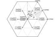
- Fig. 16 is a vector diagram illustrating a group of voltage vectors on an orthogonal d-q coordinate system.
- the group of voltage vectors can be expressed as shown in Figure 17 by expressing the first switching state, the second switching state, and the third switching state with the symbols "P", "0", and "N", respectively, and listing them in the order of U phase, V phase, and W phase.
- V0p[PPP] expresses that, with respect to the zero vector V0p, the switching state of the U-phase switching circuit 10U is "P", the switching state of the V-phase switching circuit 10V is "P”, and the switching state of the W-phase switching circuit 10W is "P".
- a voltage vector with "p” appended, such as V10p includes “P” and does not include "N”. This point applies hereinafter.
- a voltage vector with "n” appended, such as V10n includes "N" and does not include "P".
- a voltage vector with “o” appended such as V0o, includes “0” and does not include “P” or “N".
- the switching state of the switching circuit 10 is "P”
- the potential of the third connection point 13 in the switching circuit 10 is the potential of the positive pole P1 of the DC power supply unit 3.
- the switching state of the switching circuit 10 is "N”
- the potential of the third connection point 13 in the switching circuit 10 is the potential of the negative pole N1 of the DC power supply unit 3.
- the switching state of the switching circuit 10 is "0"
- the potential of the third connection point 13 in the switching circuit 10 is the potential of the intermediate potential point M1 of the DC power supply unit 3.
- V1, V2, V3, V4, V5, and V6 can be expressed as V1[PNN], V2[PPN], V3[NPN], V4[NPP], V5[NNP], and V6[PNP], respectively.
- Voltage vectors that do not have "p,” "n,” or "o” added after the number added to "V,” such as V1[PNN], V2[PPN], V3[NPN], V4[NPP], V5[NNP], and V6[PNP] include "P" and "N” as the switching states of the three phases.
- the 12 voltage vectors V7p, V7n, V8p, V8n, V9p, V9n, V10p, V10n, V11p, V11n, V12p, and V12n can be expressed as V7p[P00], V7n[0NN], V8p[PP0], V8n[00N], V9p[0P0], V9n[N0N], V10p[0PP], V10n[N00], V11p[00P], V11n[NN0], V12p[P0P], and V12n[0N0], respectively.
- V13, V14, V15, V16, V17, and V18 can be expressed as V13[P0N], V14[0PN], V15[NP0], V16[N0P], V17[0NP], and V18[PN0], respectively.
- the control unit 60 converts the instantaneous value of the command voltage related to the output voltage of each of the multiple inverter circuits 1 into a command voltage vector V * (see FIG. 18). If the d-axis component of the command voltage vector V * on the orthogonal d-q coordinate system is Vd and the q-axis component of the command voltage vector V * on the orthogonal d-q coordinate system is Vq, the command voltage vector V * can be calculated using the following formula (1).
- the control unit 60 selects a plurality of (e.g., five) voltage vectors that are adjacent to the command voltage vector V * from the group of voltage vectors.
- the plurality of voltage vectors are V8p[PP0], V8n[00N], V13[P0N], V7p[P00], and V7n[0NN].
- the angle between the command voltage vector V * and a voltage vector (hereinafter also referred to as a voltage vector VV1) closest to the command voltage vector V * is smaller than 30 degrees.
- the control unit 60 makes the composite vector of the vectors of the vertices of the equilateral triangle surrounding the command voltage vector V * coincide with the command voltage vector V * within a predetermined control period Ts. That is, the control unit 60 makes the composite vector of the voltage vector VV1 (V8p[PP0] and V8n[00N] in the example of FIG. 18), the voltage vector V13[P0N], and the voltage vector V7p[P00] and V7n[0NN] coincide with the command voltage vector V * .
- the control period Ts is one period of the carrier signal.
- the switching state of only one of the U phase, V phase, and W phase changes between "P" and "0” or between "0” and “N", and the same voltage vector is output twice.
- the distribution time of the voltage vectors V8p and V8n for the control period Ts is T0
- the distribution time of the voltage vector V13 is T1
- the distribution time of the voltage vectors V7p and V7n is T2
- the voltage vectors at the vertices of the equilateral triangle surrounding the command voltage vector V * are Va, Vb, and Vc
- the magnitude of the command voltage vector V * is V
- the angle is ⁇ , T0, T1, and T2 are determined so as to satisfy the formulas (2) and (3).
- "j" is an imaginary unit.
- the voltage vector Va is the voltage vector V8p[PP0] and V8n[00N]
- the voltage vector Vb is the voltage vector V13[P0N]
- the voltage vector Vc is the voltage vector V7p[P00] and V7n[0NN].
- the control unit 60 transitions from the third control mode to the first control mode via the second control mode.
- the above configuration makes it possible to suppress voltage drops in each of the multiple first bootstrap circuits 71, the multiple second bootstrap circuits 72, and the multiple third bootstrap circuits 73.
- Vdc/2 is divided between the third switching element Q3 and the fourth switching element Q4 while maintaining the voltage applied to the third switching element Q3 in the third control mode.
- the control unit 60 sets the length T4 of the on-period of the fourth switching element Q4 to a length between 90% and 110% of the CR time constant of the third bootstrap circuit 73 that supplies voltage to the third gate driver 63.
- the above configuration makes it possible to miniaturize the third gate driver 63.
- the DC-DC converter 91 included in the power supply unit 9 supplies voltage to the multiple fourth gate drivers 64 and the multiple third bootstrap circuits 73. This makes it possible for the power conversion device 100 according to the embodiment to be compact while suppressing voltage drops in each of the multiple third bootstrap circuits 73.
- Each of the first switching elements Q1, the second switching elements Q2, the third switching elements Q3, and the fourth switching elements Q4 is not limited to a MOSFET, and may be, for example, an IGBT (Insulated Gate Bipolar Transistor).
- the control terminal, the first main terminal, and the second main terminal of each of the first switching elements Q1, the second switching elements Q2, the third switching elements Q3, and the fourth switching elements Q4 are the gate terminal, the collector terminal, and the emitter terminal, respectively.
- control unit 60 is not limited to being configured to perform voltage vector control, but may also be configured to perform PWM control.
- each of the multiple first bootstrap circuits 71 may include a Zener diode Z17, but may not include the Zener diode Z17.Furthermore, each of the multiple second bootstrap circuits 72 may include a Zener diode Z27, but may not include the Zener diode Z27.Furthermore, each of the multiple third bootstrap circuits 73 may include a Zener diode Z37, but may not include the Zener diode Z37.
- each of the multiple first bootstrap circuits 71 includes a resistor R17, and is configured such that the CR time constant is determined by the capacitance of capacitor C17 and the resistance value of resistor R17, but it may also be configured such that the CR time constant is determined by the capacitance of capacitor C17 and the ESR (Equivalent Series Resistance) of capacitor C17 without including resistor R17.
- each of the multiple second bootstrap circuits 72 includes a resistor R27, and is configured such that the CR time constant is determined by the capacitance of capacitor C27 and the resistance value of resistor R27, but it may also be configured such that the CR time constant is determined by the capacitance of capacitor C27 and the ESR of capacitor C27 without including resistor R27.
- each of the multiple third bootstrap circuits 73 includes a resistor R37, and the CR time constant is determined by the capacitance of the capacitor C37 and the resistance value of the resistor R37.
- the configuration may be such that the CR time constant is determined by the capacitance of the capacitor C37 and the ESR of the capacitor C37 without including the resistor R37.
- the power conversion device 100 is not limited to a configuration having one DC-DC converter 91 as in FIG. 1 as the power supply unit 9 that supplies voltage to the three fourth gate drivers 64, but may be a configuration having multiple (three) DC-DC converters 91, for example, as in the power conversion device 100 according to the modified example shown in FIG. 19.
- the multiple DC-DC converters 91 correspond to the multiple (three) fourth gate drivers 64 and supply voltage to the corresponding fourth gate drivers 64.
- the anode of the diode D17 is connected to the positive terminal of the corresponding DC-DC converter 91 among the multiple DC-DC converters 91.
- the anode of the diode D27 is connected to the positive terminal of the corresponding DC-DC converter 91 among the multiple DC-DC converters 91.
- the anode of the diode D37 is connected to the positive terminal of the corresponding DC-DC converter 91 among the multiple DC-DC converters 91.
- the power conversion device 100 may also include multiple DC-DC converters in place of each of the multiple first bootstrap circuits 71.
- the power conversion device 100 may also include multiple DC-DC converters in place of each of the multiple second bootstrap circuits 72.
- the power conversion device 100 is not limited to a configuration including multiple switching circuits 10, and may be configured to include one switching circuit 10.
- the power conversion device 100 is configured to include one switching circuit 10 instead of multiple switching circuits 10, there is also one each of the first gate driver 61, second gate driver 62, third gate driver 63, and fourth gate driver 64, and there is also one each of the first bootstrap circuit 71, second bootstrap circuit 72, and third bootstrap circuit 73.
- a DC-DC converter may be provided in place of each of the first bootstrap circuit 71 and second bootstrap circuit 72.
- the power conversion device 100 may be a three-level or higher power conversion device, for example, a five-level inverter.
- the power conversion device (100) includes a DC power supply unit (3), a switching circuit (10), a first diode (D5), a second diode (D6), an output terminal (41), a first gate driver (61), a second gate driver (62), a third gate driver (63), a fourth gate driver (64), a bootstrap circuit (third bootstrap circuit 73), a power supply unit (9), and a control unit (60).
- the DC power supply unit (3) has a positive electrode (P1), a negative electrode (N1), and an intermediate potential point (M1).
- the switching circuit (10) has a first switching element (Q1), a second switching element (Q2), a third switching element (Q3), and a fourth switching element (Q4).
- a first switching element (Q1), a second switching element (Q2), a third switching element (Q3), and a fourth switching element (Q4) are connected in series between the positive electrode (P1) and the negative electrode (N1) in the order of the first switching element (Q1), the second switching element (Q2), the third switching element (Q3), and the fourth switching element (Q4) from the positive electrode (P1).
- the first diode (D5) has a cathode connected to a first connection point (11) between the first switching element (Q1) and the second switching element (Q2), and an anode connected to an intermediate potential point (M1).
- the second diode (D6) has an anode connected to a second connection point (12) between the third switching element (Q3) and the fourth switching element (Q4), and a cathode connected to the intermediate potential point (M1).
- the output terminal (41) is connected to a third connection point (13) between the second switching element (Q2) and the third switching element (Q3), and is connected to an AC load (RA1).
- the first gate driver (61) drives the first switching element (Q1).
- the second gate driver (62) drives the second switching element (Q2).
- the third gate driver (63) drives the third switching element (Q3).
- the fourth gate driver (64) drives the fourth switching element (Q4).
- the bootstrap circuit (third bootstrap circuit 73) supplies a voltage to the third gate driver (63).
- the power supply unit (9) supplies a voltage to the bootstrap circuit (third bootstrap circuit 73) and the fourth gate driver (64).
- the control unit (60) controls the first gate driver (61), the second gate driver (62), the third gate driver (63), and the fourth gate driver (64).
- the control unit (60) has a first control mode, a second control mode, and a third control mode. In the first control mode, the control unit (60) turns on the first switching element (Q1), turns on the second switching element (Q2), turns off the third switching element (Q3), and turns off the fourth switching element (Q4).
- the control unit (60) turns off the first switching element (Q1), turns on the second switching element (Q2), turns on the third switching element (Q3), and turns off the fourth switching element (Q4).
- the control unit (60) turns off the first switching element (Q1), turns on the second switching element (Q2), turns off the third switching element (Q3), and turns on the fourth switching element (Q4).
- the control unit (60) transitions from the third control mode to the first control mode via the second control mode.
- the power conversion device (100) according to the second aspect further includes a bootstrap circuit (first bootstrap circuit 71) that supplies a voltage to the first gate driver (61) and a bootstrap circuit (second bootstrap circuit 72) that supplies a voltage to the second gate driver (62) in the first aspect.
- first bootstrap circuit 71 that supplies a voltage to the first gate driver (61)
- second bootstrap circuit 72 that supplies a voltage to the second gate driver (62) in the first aspect.
- This aspect makes it possible to further reduce the size of the power conversion device (100).
- the control unit (60) sets the length (T4) of the on-period of the fourth switching element (Q4) in the third control mode to be 90% or more and 110% or less of the CR time constant of the bootstrap circuit (third bootstrap circuit 73) that supplies voltage to the third gate driver (63).
- the bootstrap circuit (third bootstrap circuit 73) that supplies a voltage to the third gate driver (63) includes a capacitor (C37) and a diode (D37) connected in series to the capacitor (C37).
- the bootstrap circuit (third bootstrap circuit 73) that supplies voltage to the third gate driver (63) in the fourth aspect further includes a resistor (R37) connected in series with the capacitor (C37).
- the power supply unit (9) includes a DC-DC converter (91).
- the power conversion device (100) in the first aspect, includes a plurality of switching circuits (10), a plurality of first gate drivers (61), a plurality of second gate drivers (62), a plurality of third gate drivers (63), a plurality of fourth gate drivers (64), and a plurality of bootstrap circuits (third bootstrap circuits 73).
- the power supply unit (9) supplies voltage to at least the plurality of fourth gate drivers (64) and the plurality of bootstrap circuits (third bootstrap circuits 73).
- This embodiment makes it possible to suppress voltage drops in each of the multiple bootstrap circuits (third bootstrap circuit 73) while achieving miniaturization.
Landscapes
- Engineering & Computer Science (AREA)
- Power Engineering (AREA)
- Inverter Devices (AREA)
- Power Conversion In General (AREA)
Priority Applications (3)
| Application Number | Priority Date | Filing Date | Title |
|---|---|---|---|
| JP2025520455A JPWO2024236980A1 (https=) | 2023-05-16 | 2024-04-15 | |
| CN202480030439.0A CN121153192A (zh) | 2023-05-16 | 2024-04-15 | 电力转换器 |
| EP24806934.6A EP4716086A1 (en) | 2023-05-16 | 2024-04-15 | Electric power conversion apparatus |
Applications Claiming Priority (2)
| Application Number | Priority Date | Filing Date | Title |
|---|---|---|---|
| JP2023081077 | 2023-05-16 | ||
| JP2023-081077 | 2023-05-16 |
Publications (1)
| Publication Number | Publication Date |
|---|---|
| WO2024236980A1 true WO2024236980A1 (ja) | 2024-11-21 |
Family
ID=93518953
Family Applications (1)
| Application Number | Title | Priority Date | Filing Date |
|---|---|---|---|
| PCT/JP2024/015024 Ceased WO2024236980A1 (ja) | 2023-05-16 | 2024-04-15 | 電力変換装置 |
Country Status (4)
| Country | Link |
|---|---|
| EP (1) | EP4716086A1 (https=) |
| JP (1) | JPWO2024236980A1 (https=) |
| CN (1) | CN121153192A (https=) |
| WO (1) | WO2024236980A1 (https=) |
Cited By (1)
| Publication number | Priority date | Publication date | Assignee | Title |
|---|---|---|---|---|
| WO2026078953A1 (ja) * | 2024-10-08 | 2026-04-16 | パナソニックIpマネジメント株式会社 | マルチレベルインバータ |
Citations (4)
| Publication number | Priority date | Publication date | Assignee | Title |
|---|---|---|---|---|
| JP2013236544A (ja) * | 2011-09-30 | 2013-11-21 | Sharp Corp | スイッチング電源装置 |
| JP2018133876A (ja) | 2017-02-14 | 2018-08-23 | 株式会社東芝 | 3レベル中性点クランプ形インバータのスイッチング素子駆動回路 |
| WO2024053452A1 (ja) * | 2022-09-09 | 2024-03-14 | パナソニックIpマネジメント株式会社 | マルチレベルインバータ |
| WO2024053453A1 (ja) * | 2022-09-09 | 2024-03-14 | パナソニックIpマネジメント株式会社 | マルチレベルインバータ |
-
2024
- 2024-04-15 CN CN202480030439.0A patent/CN121153192A/zh active Pending
- 2024-04-15 JP JP2025520455A patent/JPWO2024236980A1/ja active Pending
- 2024-04-15 EP EP24806934.6A patent/EP4716086A1/en active Pending
- 2024-04-15 WO PCT/JP2024/015024 patent/WO2024236980A1/ja not_active Ceased
Patent Citations (4)
| Publication number | Priority date | Publication date | Assignee | Title |
|---|---|---|---|---|
| JP2013236544A (ja) * | 2011-09-30 | 2013-11-21 | Sharp Corp | スイッチング電源装置 |
| JP2018133876A (ja) | 2017-02-14 | 2018-08-23 | 株式会社東芝 | 3レベル中性点クランプ形インバータのスイッチング素子駆動回路 |
| WO2024053452A1 (ja) * | 2022-09-09 | 2024-03-14 | パナソニックIpマネジメント株式会社 | マルチレベルインバータ |
| WO2024053453A1 (ja) * | 2022-09-09 | 2024-03-14 | パナソニックIpマネジメント株式会社 | マルチレベルインバータ |
Non-Patent Citations (1)
| Title |
|---|
| See also references of EP4716086A1 |
Cited By (1)
| Publication number | Priority date | Publication date | Assignee | Title |
|---|---|---|---|---|
| WO2026078953A1 (ja) * | 2024-10-08 | 2026-04-16 | パナソニックIpマネジメント株式会社 | マルチレベルインバータ |
Also Published As
| Publication number | Publication date |
|---|---|
| CN121153192A (zh) | 2025-12-16 |
| JPWO2024236980A1 (https=) | 2024-11-21 |
| EP4716086A1 (en) | 2026-03-25 |
Similar Documents
| Publication | Publication Date | Title |
|---|---|---|
| WO2024053453A1 (ja) | マルチレベルインバータ | |
| WO2024053452A1 (ja) | マルチレベルインバータ | |
| US7495938B2 (en) | DC voltage balance control for three-level NPC power converters with even-order harmonic elimination scheme | |
| US9431923B2 (en) | Power converter | |
| JPH09182441A (ja) | 三相整流装置 | |
| JPH11220886A (ja) | マルチレベル形電力変換器 | |
| WO2024162204A1 (ja) | 電力変換装置 | |
| WO2024009827A1 (ja) | 電力変換装置 | |
| WO2024236980A1 (ja) | 電力変換装置 | |
| WO2022029869A1 (ja) | 電力変換装置 | |
| WO2025004696A1 (ja) | マルチレベルインバータ | |
| WO2024253051A1 (ja) | マルチレベルインバータ | |
| WO2025004601A1 (ja) | スイッチング素子駆動回路及び電力変換装置 | |
| WO2025070037A1 (ja) | マルチレベルインバータ | |
| WO2025100234A1 (ja) | マルチレベルインバータ | |
| WO2025197328A1 (ja) | マルチレベルインバータ | |
| WO2025100235A1 (ja) | マルチレベルインバータ | |
| WO2026078953A1 (ja) | マルチレベルインバータ | |
| WO2025249443A1 (ja) | スイッチング素子駆動回路及び電力変換装置 | |
| WO2026078955A1 (ja) | マルチレベルインバータ | |
| WO2026018574A1 (ja) | スイッチング素子駆動回路及び電力変換装置 | |
| WO2026078954A1 (ja) | マルチレベルインバータ | |
| JP7667713B2 (ja) | インバータ装置 | |
| WO2024247827A1 (ja) | 電力変換装置 | |
| WO2025041615A1 (ja) | 電力変換装置 |
Legal Events
| Date | Code | Title | Description |
|---|---|---|---|
| 121 | Ep: the epo has been informed by wipo that ep was designated in this application |
Ref document number: 24806934 Country of ref document: EP Kind code of ref document: A1 |
|
| ENP | Entry into the national phase |
Ref document number: 2025520455 Country of ref document: JP Kind code of ref document: A |
|
| WWE | Wipo information: entry into national phase |
Ref document number: 2024806934 Country of ref document: EP |
|
| NENP | Non-entry into the national phase |
Ref country code: DE |
|
| ENP | Entry into the national phase |
Ref document number: 2024806934 Country of ref document: EP Effective date: 20251216 |
|
| ENP | Entry into the national phase |
Ref document number: 2024806934 Country of ref document: EP Effective date: 20251216 |
|
| ENP | Entry into the national phase |
Ref document number: 2024806934 Country of ref document: EP Effective date: 20251216 |
|
| ENP | Entry into the national phase |
Ref document number: 2024806934 Country of ref document: EP Effective date: 20251216 |
|
| ENP | Entry into the national phase |
Ref document number: 2024806934 Country of ref document: EP Effective date: 20251216 |
|
| ENP | Entry into the national phase |
Ref document number: 2024806934 Country of ref document: EP Effective date: 20251216 |
|
| ENP | Entry into the national phase |
Ref document number: 2024806934 Country of ref document: EP Effective date: 20251216 |
|
| ENP | Entry into the national phase |
Ref document number: 2024806934 Country of ref document: EP Effective date: 20251216 |
|
| WWP | Wipo information: published in national office |
Ref document number: 2024806934 Country of ref document: EP |