WO2024232192A1 - 表面弾性波デバイス用複合基板 - Google Patents
表面弾性波デバイス用複合基板 Download PDFInfo
- Publication number
- WO2024232192A1 WO2024232192A1 PCT/JP2024/013466 JP2024013466W WO2024232192A1 WO 2024232192 A1 WO2024232192 A1 WO 2024232192A1 JP 2024013466 W JP2024013466 W JP 2024013466W WO 2024232192 A1 WO2024232192 A1 WO 2024232192A1
- Authority
- WO
- WIPO (PCT)
- Prior art keywords
- substrate
- thin film
- single crystal
- acoustic wave
- surface acoustic
- Prior art date
- Legal status (The legal status is an assumption and is not a legal conclusion. Google has not performed a legal analysis and makes no representation as to the accuracy of the status listed.)
- Ceased
Links
Images


Classifications
-
- H—ELECTRICITY
- H03—ELECTRONIC CIRCUITRY
- H03H—IMPEDANCE NETWORKS, e.g. RESONANT CIRCUITS; RESONATORS
- H03H9/00—Networks comprising electromechanical or electro-acoustic elements; Electromechanical resonators
- H03H9/02—Details
- H03H9/02535—Details of surface acoustic wave devices
- H03H9/02543—Characteristics of substrate, e.g. cutting angles
- H03H9/02574—Characteristics of substrate, e.g. cutting angles of combined substrates, multilayered substrates, piezoelectrical layers on not-piezoelectrical substrate
-
- H—ELECTRICITY
- H03—ELECTRONIC CIRCUITRY
- H03H—IMPEDANCE NETWORKS, e.g. RESONANT CIRCUITS; RESONATORS
- H03H9/00—Networks comprising electromechanical or electro-acoustic elements; Electromechanical resonators
- H03H9/02—Details
- H03H9/02535—Details of surface acoustic wave devices
- H03H9/02543—Characteristics of substrate, e.g. cutting angles
- H03H9/02559—Characteristics of substrate, e.g. cutting angles of lithium niobate or lithium-tantalate substrates
-
- H—ELECTRICITY
- H03—ELECTRONIC CIRCUITRY
- H03H—IMPEDANCE NETWORKS, e.g. RESONANT CIRCUITS; RESONATORS
- H03H9/00—Networks comprising electromechanical or electro-acoustic elements; Electromechanical resonators
- H03H9/02—Details
- H03H9/02535—Details of surface acoustic wave devices
- H03H9/02818—Means for compensation or elimination of undesirable effects
- H03H9/02834—Means for compensation or elimination of undesirable effects of temperature influence
-
- H—ELECTRICITY
- H03—ELECTRONIC CIRCUITRY
- H03H—IMPEDANCE NETWORKS, e.g. RESONANT CIRCUITS; RESONATORS
- H03H9/00—Networks comprising electromechanical or electro-acoustic elements; Electromechanical resonators
- H03H9/02—Details
- H03H9/02535—Details of surface acoustic wave devices
- H03H9/02818—Means for compensation or elimination of undesirable effects
- H03H9/02866—Means for compensation or elimination of undesirable effects of bulk wave excitation and reflections
-
- H—ELECTRICITY
- H03—ELECTRONIC CIRCUITRY
- H03H—IMPEDANCE NETWORKS, e.g. RESONANT CIRCUITS; RESONATORS
- H03H9/00—Networks comprising electromechanical or electro-acoustic elements; Electromechanical resonators
- H03H9/25—Constructional features of resonators using surface acoustic waves
-
- H—ELECTRICITY
- H10—SEMICONDUCTOR DEVICES; ELECTRIC SOLID-STATE DEVICES NOT OTHERWISE PROVIDED FOR
- H10N—ELECTRIC SOLID-STATE DEVICES NOT OTHERWISE PROVIDED FOR
- H10N30/00—Piezoelectric or electrostrictive devices
- H10N30/80—Constructional details
- H10N30/85—Piezoelectric or electrostrictive active materials
- H10N30/853—Ceramic compositions
Definitions
- the present invention relates to a composite substrate for surface acoustic wave devices that includes a piezoelectric single crystal thin film and a support substrate.
- a surface acoustic wave (SAW) device is used as a frequency adjustment/selection component, in which an interdigital transducer (IDT) for exciting a surface acoustic wave is formed on a piezoelectric substrate.
- IDT interdigital transducer
- Surface acoustic wave devices are required to be small, have low insertion loss, and block unwanted waves, and use piezoelectric materials such as lithium tantalate (LiTaO 3 ; LT) and lithium niobate (LiNbO 3 ; LN).
- the piezoelectric materials used in surface acoustic wave devices must have sufficiently small temperature-induced characteristic variations. Also, to prevent unnecessary noise from spilling out between bands, filters, duplexers, and multiplexers must have as small an insertion loss as possible, and the shoulder characteristics of filters must be extremely steep, requiring the resonators that make up the filters to have a high Q value (Quality Factor). Filters are also required to be able to handle a wide bandwidth depending on the band being used.
- Patent Document 1 discloses an acoustic wave device having a piezoelectric film, the acoustic wave device comprising a support substrate, a high acoustic velocity film formed on the support substrate and having a bulk wave acoustic velocity faster than the acoustic wave acoustic velocity propagating through the piezoelectric film, a low acoustic velocity film laminated on the high acoustic velocity film and having a bulk wave acoustic velocity slower than the bulk wave acoustic velocity propagating through the piezoelectric film, the piezoelectric film laminated on the low acoustic velocity film, and an IDT electrode formed on one side of the piezoelectric film.
- Patent Document 2 discloses a piezoelectric element including a support substrate, a medium layer laminated on the support substrate, a piezoelectric body laminated on the medium layer and through which bulk waves propagate, and an IDT electrode formed on one side of the piezoelectric body, the medium layer being a low-velocity medium in which the propagation velocity of bulk waves identical to the bulk waves that are the main component of the elastic waves is slower than the sound velocity of the elastic waves propagating through the piezoelectric body, and an IDT electrode formed on one side of the piezoelectric body, the medium layer being a low-velocity medium in which the propagation velocity of bulk waves identical to the bulk waves that are the main component of the elastic waves is slower than the sound velocity of the elastic waves propagating through the piezoelectric body,
- the elastic wave device disclosed includes a high-speed medium, and the medium layer is formed so that the sound velocity of the main vibration mode in the elastic wave device in which the medium layer is formed satisfies VL ⁇ sound velocity of main vibration mode ⁇
- the present invention was made in consideration of these circumstances, and aims to provide a composite substrate for surface acoustic wave devices that has low loss in the filter passband, few spurious components, and has excellent performance and high reliability.
- the inventors have found that by providing a piezoelectric single crystal thin film, a support substrate, and at least one intermediate layer between the piezoelectric single crystal thin film and the support substrate, and by specifying the total thickness of the intermediate layer and the attenuation of longitudinal waves, the loss in the passband of the filter can be reduced and high reliability can be obtained, and have completed the present invention.
- the gist of the present invention is as follows.
- a composite substrate for a surface acoustic wave device comprising a piezoelectric single crystal thin film, a support substrate, and at least one intermediate layer provided between the piezoelectric single crystal thin film and the support substrate, wherein the intermediate layer is in contact with the piezoelectric single crystal thin film, the total thickness of the intermediate layer is not more than twice the thickness of the wavelength of the surface acoustic wave, and the attenuation of the longitudinal wave of the intermediate layer calculated at frequencies from 40 GHz to 60 GHz by the Brillouin oscillation method is not more than 8 ⁇ 10 -2 (nm -1 ⁇ THz -2 ).
- the composite substrate for surface acoustic wave devices according to any one of [1] to [4], wherein the main component of the piezoelectric single crystal thin film is lithium tantalate or lithium niobate.
- the support substrate is any one of a silicon substrate, a sapphire substrate, an alumina substrate, a silicon carbide substrate, an aluminum nitride substrate, a silicon nitride substrate, and a quartz substrate [1] to [5].
- a composite substrate for a surface acoustic wave device is any one of a silicon substrate, a sapphire substrate, an alumina substrate, a silicon carbide substrate, an aluminum nitride substrate, a silicon nitride substrate, and a quartz substrate [1] to [5].
- the present invention provides a composite substrate for surface acoustic wave devices that has low loss in the filter passband and is highly reliable.
- FIG. 1 is a diagram showing an example of the spectrum of Brillouin oscillations of a SiO 1.7 thin film.
- FIG. 2 is a diagram showing a waveform obtained by Fourier transform of only the reflected light of ultrasonic waves (longitudinal waves) in a thin film.
- FIG. 3 is a diagram showing the dependency relationship between the LSAW sound velocity of a thin film and the value obtained by normalizing the thin film thickness to the wavelength of ultrasonic waves (thin film thickness/wavelength), and the calculation results of the sound velocity of elastic waves obtained by the finite element method.
- FIG. 1 is a diagram showing an example of the spectrum of Brillouin oscillations of a SiO 1.7 thin film.
- FIG. 2 is a diagram showing a waveform obtained by Fourier transform of only the reflected light of ultrasonic waves (longitudinal waves) in a thin film.
- FIG. 3 is a diagram showing the dependency relationship between the LSAW sound velocity of a thin film and the value obtained by
- FIG. 4 is a diagram showing an example of a calculation result of a displacement distribution of an elastic wave in which the energy is concentrated in the surface layer of a thin film having a SiO 1.7 thin film/(111) Si substrate structure.
- FIG. 5 is a diagram showing an example of a cross-sectional TEM observation photograph of the composite substrate produced in Example 1.
- FIG. 6 is a diagram showing a composite substrate having Al fine electrodes formed on the surface.
- FIG. 7 is a diagram showing the resonance waveform (input impedance (Zin) and Q value) of the SAW obtained in Example 1.
- FIG. 8 is a diagram showing the resonance waveform (input impedance (Zin) and Q value) of the SAW obtained in Example 2.
- FIG. 9 is a diagram showing the resonance waveform (input impedance (Zin) and Q value) of the SAW obtained in Comparative Example 1.
- FIG. 10 is a diagram showing the resonance waveform (input impedance (Zin) and Q value) of the SAW obtained in Comparative Example 2.
- the composite substrate for a surface acoustic wave device of the present invention is a composite substrate comprising a piezoelectric single crystal thin film, a support substrate, and at least one intervening layer provided between the piezoelectric single crystal thin film and the support substrate, wherein the intervening layer is in contact with the piezoelectric single crystal thin film, the total thickness of the intervening layer is not more than twice the thickness of the wavelength of the surface acoustic wave, and the attenuation of the longitudinal wave of the intervening layer calculated at frequencies of 40 GHz to 60 GHz by the Brillouin oscillation method is not more than 8 ⁇ 10 -2 (nm -1 ⁇ THz -2 ).
- the piezoelectric single crystal thin film in the surface acoustic wave device composite substrate according to one embodiment of the present invention is not particularly limited as long as it can be used as a piezoelectric film, but it is preferable that the main component is lithium tantalate ( LiTaO3 :LT) or lithium niobate ( LiNbO3 :LN).
- the main component is lithium tantalate ( LiTaO3 :LT) or lithium niobate ( LiNbO3 :LN).
- the main component of the piezoelectric single crystal thin film is lithium tantalate or lithium niobate means that 50 mass % or more of the components constituting the piezoelectric single crystal thin film is lithium tantalate or lithium niobate.
- the components of the piezoelectric single crystal thin film may contain iron, magnesium, etc., as components other than lithium tantalate and lithium niobate.
- the piezoelectric single crystal thin film contains 120 ppm or less of iron.
- the electric field at which the polarization of the piezoelectric single crystal thin film is destroyed i.e., the coercive electric field
- the iron content is 10 ppm or more and 120 ppm or less, and even more preferable that it is 50 ppm or more and 100 ppm or less.
- the initial volume resistivity of the piezoelectric single crystal thin film is preferably 2 ⁇ 10 11 ⁇ cm or less.
- the constant temperature resistance of the composite substrate for surface acoustic wave devices of the present invention can be improved.
- the initial volume resistivity of the piezoelectric single crystal thin film is more preferably 2 ⁇ 10 10 ⁇ cm or more and 2 ⁇ 10 11 ⁇ cm or less, and even more preferably 2 ⁇ 10 10 ⁇ cm or more and 1 ⁇ 10 11 ⁇ cm or less.
- the support substrate in the surface acoustic wave device composite substrate can be any of a silicon substrate, a sapphire substrate, an alumina substrate, a silicon carbide substrate, an aluminum nitride substrate, a silicon nitride substrate, and a quartz substrate.
- a surface acoustic wave resonator manufactured using a composite substrate for a surface acoustic wave device using the above-mentioned substrate as a supporting substrate has a high Q value, and out-of-band spurious emissions are further suppressed, and a surface acoustic wave device with excellent temperature characteristics can be obtained.
- the support substrate may be made of a single crystal Si and a polysilicon layer formed on the single crystal Si.
- the thickness of the polysilicon layer is preferably 0.2 ⁇ m or more and 2 ⁇ m or less, more preferably 0.5 ⁇ m or more and 1.9 ⁇ m or less, and further preferably 0.5 ⁇ m or more and 1.2 ⁇ m or less.
- the surface acoustic wave device composite substrate of the present invention includes an intermediate layer between the piezoelectric single crystal thin film and a support substrate, and the intermediate layer is provided in contact with the piezoelectric single crystal thin film.
- the intermediate layer in the surface acoustic wave device composite substrate of one embodiment of the present invention is preferably either SiOx (1.8 ⁇ x ⁇ 2.05) or SiOyNz (0.02 ⁇ z/(y+z) ⁇ 0.1).
- the surface acoustic wave device composite substrate of the present invention also includes at least one intermediate layer.
- the intermediate layer may be one layer or two or more layers, and when two or more layers are included, each layer may be made of the same material or different materials.
- the content of Li ions in the intermediate layer is preferably 1 ⁇ 10 17 atom/cm 3 or less. Li ions mainly diffuse from the piezoelectric single crystal thin film to the intermediate layer, but by making the content of Li ions in the intermediate layer 1 ⁇ 10 17 atom/cm 3 or less, softening of the intermediate layer can be prevented and in-band and out-of-band spurious can be suppressed.
- the thickness of the intervening layer is equal to or less than twice the wavelength of the surface acoustic wave of the intervening layer when there is a single intervening layer, and equal to or less than twice the wavelength of the surface acoustic wave of the intervening layer when there are two or more intervening layers. If the thickness of the intervening layer exceeds twice the wavelength of the surface acoustic wave of the intervening layer, the acoustic wave is more likely to be trapped within the intervening layer, resulting in a problem of large out-of-band spurious.
- the total thickness of the intervening layer is preferably equal to or less than twice the wavelength of the surface acoustic wave, and more preferably equal to or less than once.
- the attenuation of longitudinal waves in the intermediate layer calculated at frequencies of 40 GHz to 60 GHz by the Brillouin oscillation method is 8 ⁇ 10 ⁇ 2 (nm ⁇ 1 ⁇ THz ⁇ 2 ) or less.
- the acoustic attenuation of the longitudinal waves in the intermediate layer is large, the acoustic waves are easily trapped in the intermediate layer.
- the surface acoustic wave resonator made of the composite substrate for surface acoustic wave devices of the present invention has a problem of large out-of-band spurious.
- the Q value of the surface acoustic wave resonator is high and the out-of-band spurious can be further suppressed.
- the attenuation of the longitudinal waves in the intermediate layer is preferably 2 ⁇ 10 ⁇ 2 (nm ⁇ 1 ⁇ THz ⁇ 2 ) or less, and more preferably 0.5 ⁇ 10 ⁇ 2 (nm ⁇ 1 ⁇ THz ⁇ 2 ) or less.
- the sound velocity of the shear waves in the intervening layer is faster than the sound velocity of the slow shear waves in the piezoelectric single crystal thin film.
- the shear waves (bulk waves) in the intervening layer faster than the slow shear waves (bulk waves) in the piezoelectric single crystal thin film, it is possible to improve the loss in the passband of the surface acoustic wave filter obtained using the composite substrate for surface acoustic wave devices. If the shear waves in the intervening layer are slower than the slow shear waves in the piezoelectric single crystal thin film, there is a concern that the acoustic waves will be more likely to be trapped in the intervening layer. Note that, because the piezoelectric single crystal thin film is an anisotropic material, there are two types of shear waves in the piezoelectric single crystal thin film: fast shear waves and slow shear waves.
- the slow transverse wave of 46° rotated Y-cut LiTaO3 is 3330 m/s.
- SiO1.85 or SiO1.94N0.06 as an example of an intervening layer, the sound velocity of the transverse wave of SiO1.85 or SiO1.94N0.06 is high, at 3850 m/ s and 3750 m/s, respectively.
- the sound velocity of the shear wave of SiO1.85 or SiO1.94N0.06 will be described in detail later, but it can be determined from the measured shear wave sound velocity of LSAW of the piezoelectric single crystal thin film using a linear convergent beam ultrasonic microscope and analysis by the finite element method, as described in, for example, Tatsuya Omori1, Kensuke Sakamoto, Satoshi Suzuki, Jun-ichi Kushibiki, Satoru Matsuda, and Ken-ya Hashimoto, "Characterization of Elastic Properties of SiO2 Thin Films by Ultrasonic Microscopy".
- the sound velocity of the transverse waves in the intermediate layer can be made faster than the sound velocity of the slow transverse waves in the piezoelectric single crystal thin film.
- the attenuation of longitudinal waves in the intermediate layer was calculated at frequencies between 40 GHz and 60 GHz using the Brillouin oscillation method, the attenuation was 1.2 ⁇ 10 -2 (nm -1 ⁇ THz -2 ) for SiO 1.85 and 0.1 ⁇ 10 -2 (nm -1 ⁇ THz -2 ) for SiO 1.94 N 0.06 , indicating that the attenuation of longitudinal waves can be reduced to 8 ⁇ 10 -2 (nm -1 ⁇ THz -2 ) or less.
- Figure 1 shows an example of the Brillouin oscillation spectrum of a SiO1.7 thin film having the same composition and fabrication method as the intermediate layer, when the composition of the intermediate layer is SiO1.7 .
- the SiO 1.7 thin film (hereinafter, simply referred to as "thin film”) used in the measurement of FIG. 1 was formed on a Si substrate with a thickness of 1055 nm (the thickness is d) of SiO 1.7 thin film having the same composition and manufacturing method as the intermediate layer, and further formed an Al film of 10 nm on the SiO 1.7 thin film.
- the manufacturing method of the thin film is not particularly limited, but may be, for example, a CVD method.
- Ultra-high frequency ultrasonic waves are generated by irradiating a structure consisting of this Al film, SiO 1.7 thin film, and Si substrate with extremely short pulse light. Furthermore, delayed pulse light with a reference wavelength ( ⁇ ) of 400 nm is irradiated.
- the longitudinal wave sound velocity of the thin film can be obtained by detecting the light diffracted by the ultrasonic waves in the thin film.
- the density of the thin film and the refractive index at 400 nm were previously obtained.
- the refractive index (n) of the thin film at 400 nm was 1.728 by the prism coupler method.
- the density ( ⁇ ) of the thin film was determined by XPS (X-ray photoelectron spectroscopy) to be 2300 kg/ m3 .
- the first half of the Brillouin spectrum shown in Figure 1 shows the reflected light intensity due to diffraction by ultrasonic waves (longitudinal waves) in the thin film.
- the frequency of the ultrasonic waves (longitudinal waves) in the thin film shown in Figure 2 can be obtained. From Figure 2, the frequency (f) of the ultrasonic waves (longitudinal waves) in the thin film can be calculated to be 54.5 GHz.
- the sound velocity vl of the ultrasonic wave (longitudinal wave) in the thin film can be calculated by the following formula (1).
- vl f ⁇ /(2 ⁇ n)...Formula (1)
- the sound velocity of the ultrasonic waves (longitudinal waves) in the thin film shown in Fig. 2 calculated by formula (1) was 6325 m/s.
- the LSAW sound velocity (vertical axis) by the linear convergent beam ultrasonic microscope in FIG. 3 was obtained by forming a 2,830 nm-thick SiO 1.7 thin film having the same composition and manufacturing method as the intermediate layer on a substrate with a Si (111) orientation, and propagating the LSAW to the surface layer of the SiO 1.7 thin film/Si substrate structure via pure water as a coupler so that the linear convergent beam of the linear convergent beam of the linear convergent beam ultrasonic microscope was shifted 45 degrees clockwise from the ( 110) direction in the Si substrate plane as viewed from the thin film side.
- a ZnO film and an Al electrode which are sufficiently thin compared to the electrode period, are arranged on the surface layer of the thin film of the SiO 1.7 thin film/(111) Si substrate structure, and an elastic wave is excited in a direction shifted 45 degrees clockwise from the Si ⁇ 110> direction of the thin film-attached Si substrate, and the wavelength determined by the electrode period is changed on the model of the finite element method calculation to calculate the relationship between the elastic wave speed of the SiO 1.7 thin film/(111) Si substrate structure and the intermediate layer normalized by the wavelength.
- the elastic constant C12 obtained as above was 20 GPa. Furthermore, the result of calculating the sound velocity of the elastic wave by the finite element method when the elastic constant C12 of the SiO 1.7 thin film is 20 GPa is added to FIG. As an example, in a calculation model using the finite element method in which the elastic wave has a wavelength of 18 ⁇ m, the elastic wave has energy concentrated on the surface layer of a thin film having a SiO 1.7 thin film/(111) Si substrate configuration. FIG. 4 shows an example of the result of calculating the displacement distribution of the wave.
- the elastic constants of the Si substrate, ZnO film, and Al film were taken from the values given in the Surface Acoustic Wave Data Book (edited by the Japan Electronics Industry Industry Association), (p. 66 (ZnO), p. 165 (Si), p. 172 (Al)).
- the reflected light intensity due to diffraction by ultrasonic waves (longitudinal waves) in the thin film layer which is the first half of the Brillouin spectrum shown in Figure 1, attenuates exponentially with time. That is, in the envelope of the reflected light intensity shown by the dotted line in Figure 1, if the amplitude intensity at the time of 0 psec is A0 and the amplitude intensity at the time when the ultrasonic waves reach Si is A, the attenuation constant ( ⁇ ) of ultrasonic waves (longitudinal waves) in the thin film is described by formula (2).
- the attenuation of longitudinal waves was calculated at frequencies of 40 GHz to 60 GHz by the Brillouin oscillation method in the same manner as above.
- the acoustic attenuation of the longitudinal waves in the intermediate layer is large, the acoustic waves tend to be trapped in the intermediate layer.
- the surface acoustic wave resonator made of the composite substrate for surface acoustic wave devices has a problem of large out-of-band spurious.
- the intermediate layer according to the present invention has a high acoustic velocity and little attenuation of longitudinal waves, the acoustic waves cannot be concentrated excessively on the intermediate layer, and the wave energy can be concentrated on the piezoelectric single crystal thin film. Therefore, the Q value of the surface acoustic wave resonator using the composite substrate for surface acoustic wave devices according to the present invention is high, and out-of-band spurious is further suppressed, which is preferable.
- Example 1 A polysilicon layer of 1.7 ⁇ m was formed on the surface of a high-resistance silicon substrate having a diameter of 150 mm and a (111) orientation.
- a melt having a composition in which the amount of lithium was reduced based on the amount of lithium contained in the lithium tantalate crystal of the congruent composition was prepared, and an iron-substituted lithium tantalate crystal was grown from the melt having the adjusted composition.
- the amount of iron added was adjusted so that the iron content in the iron-substituted lithium tantalate crystal was 95 mass ppm, and a 6-inch iron-containing 42° Y-cut lithium tantalate (LT) substrate was prepared.
- the volume resistivity of the iron-containing 42° Y-cut lithium tantalate (LT) substrate was adjusted to 2.2 ⁇ 10 ⁇ cm by reduction treatment.
- the silicon substrate on which the polysilicon layer was formed and the iron-containing LT substrate having a 0.4 ⁇ m thick SiO 1.85 intervening layer were subjected to a surface activation treatment by plasma treatment.Furthermore, the silicon substrate on which the polysilicon layer was formed and the iron-containing LT substrate were bonded together with the 0.4 ⁇ m thick SiO 1.85 intervening layer to form a bonded body.
- the bonded body was heat-treated at 350° C. in nitrogen.
- the heat-treated bonded body was heated to 110° C., and a wedge was driven into one end of the ion-implanted portion of the iron-containing lithium tantalate (LT) substrate to separate it into the iron-containing lithium tantalate (LT) piezoelectric single crystal thin film layer bonded to the silicon substrate and the remaining iron-containing lithium tantalate (LT) substrate.
- the thickness of the iron-containing lithium tantalate (LT) piezoelectric single crystal thin film layer bonded to the silicon substrate after separation was measured by a spectrophotometer and found to be 0.52 ⁇ m.
- the composite substrate consisting of the iron-containing lithium tantalate (LT) piezoelectric single crystal thin film layer bonded to the silicon substrate was heated at 500° C. for 6 hours.
- FIG. 5 is a diagram showing an example of a cross-sectional TEM observation photograph of the composite substrate of Example 1 produced by the above method, and FIG. 5(b) is a further enlarged photograph of a part of FIG. 5(a).
- the amount of Li in the intermediate layer (SiO 1.85 layer) of the composite substrate manufactured by the above method was measured by secondary ion mass spectrometry (SIMS), and the maximum amount of Li in the SiO 1.85 layer was 2 ⁇ 10 16 atoms/cm 3.
- the composition ratio of the intermediate layer (SiO 1.85 layer) was determined by X-ray photoelectron spectroscopy (XPS).
- the density of the intermediate layer (SiO 1.85 layer) was determined by XPS (X-ray photoelectron spectroscopy) to be 2240 g/cm 3.
- the longitudinal wave sound velocity and attenuation of the intermediate layer (SiO 1.85 layer) were also determined by the Brillouin oscillation method.
- the longitudinal wave sound velocity of the intermediate layer (SiO 1.85 layer) was 6200 m/s, and the sound attenuation rate was 1.2 ⁇ 10 -3 (nm -1 ⁇ THz -2 ) at 55 GHz.
- the shear wave acoustic velocity of the intermediate layer (SiO 2 1.85 layer) alone was determined by a combination of a linear convergent beam ultrasonic microscope and finite element analysis, and was found to be 3850 m/s.
- an Al film was sputtered to a thickness of 0.14 ⁇ m on the surface of the composite substrate obtained above, and a resist was applied, and then a resist pattern with a line width of about 0.5 ⁇ m was formed by i-line exposure. Then, the Al was etched by dry etching to form the first layer of a one-port SAW resonator. At this time, the wavelength of the surface acoustic wave was 2 ⁇ m, and the thickness of the intermediate layer (SiO 1.85 layer) was 0.2 wavelengths. Furthermore, a second layer pad portion of an Al film having a thickness of 0.6 ⁇ m was formed on the above composite substrate by a lift-off method.
- Figure 6 shows the composite substrate with the Al fine electrodes formed on the surface.
- the electrical characteristics of the one-port SAW resonator on the iron-containing lithium tantalate (LT) piezoelectric single crystal thin film substrate bonded to the silicon substrate prepared above were measured using a network analyzer.
- the obtained SAW resonance waveform (input impedance (Zin) and Q value) is shown in Figure 7.
- the iron-containing lithium tantalate (LT) piezoelectric single crystal thin film substrate bonded to the silicon substrate with the one-port SAW resonator pattern created above was placed on a hot plate heated to 350°C for 10 minutes, then placed on a cooling plate at room temperature to cool, and the electrical characteristics of the one-port SAW resonator were measured again with a network analyzer.
- the resulting characteristics were the same as those in Table 1.
- this 350°C hot plate heating, cooling, and measurement were repeated for a total of four hours with a cumulative heating time of 350°C hot plate, and the electrical characteristics of the one-port SAW resonator after each cumulative heating time were not different from those in Table 1.
- Example 2 A composite substrate was prepared in the same manner as in Example 1, except that a 0.3 ⁇ m-thick intermediate layer having a composition of SiO 1.94 N 0.06 was used instead of the 0.4 ⁇ m-thick intermediate layer having a composition of SiO 1.85 in Example 1.
- the amount of Li in the intermediate layer ( SiO1.94N0.06 layer) of the iron-containing lithium tantalate (LT) piezoelectric single crystal thin film substrate bonded to a silicon substrate was measured by secondary ion mass spectrometry (SIMS), and the amount of Li in the SiO1.94N0.06 layer was found to be 1 x 10¹⁴ atom/cm3 or less .
- the composition ratio of the intermediate layer ( SiO1.94N0.06 layer ) was determined by X-ray photoelectron spectroscopy (XPS).
- the LT layer of the composite substrate made of the iron-containing lithium tantalate (LT) piezoelectric single crystal thin film bonded to the silicon substrate was removed, and the density of the intermediate layer (SiO 1.94 N 0.06 layer) was obtained by X-ray reflectometry (XRR).
- XRR X-ray reflectometry
- the density of the intermediate layer (SiO 1.94 N 0.06 layer) was 2210 g/cm 3.
- the LT layer of the iron-containing lithium tantalate (LT) piezoelectric single crystal thin film substrate bonded to the silicon substrate was removed, and the longitudinal wave sound velocity and attenuation of the intermediate layer (SiO 1.94 N 0.06 layer) were obtained by the Brillouin vibration method.
- the longitudinal wave sound velocity of the intermediate layer was 6190 m/s, and the sound wave attenuation rate was 1.2 ⁇ 10 ⁇ 3 (nm ⁇ 1 ⁇ THz ⁇ 2 ) at 55 GHz.
- the shear wave acoustic velocity of the SiO 1.94 N 0.06 layer alone was determined by combining the above -mentioned linear convergent beam ultrasonic microscope with finite element analysis, and was found to be 3750 m/s.
- the electrical characteristics of the one-port SAW resonator on the iron-containing lithium tantalate (LT) piezoelectric single crystal thin film substrate bonded to the silicon substrate prepared above were measured using a network analyzer.
- the obtained SAW resonance waveform (input impedance (Zin) and Q value) is shown in Figure 8.
- the wavelength of the surface acoustic wave is 2 ⁇ m
- the thickness of the intermediate layer SiO 1.94 N 0.06 layer
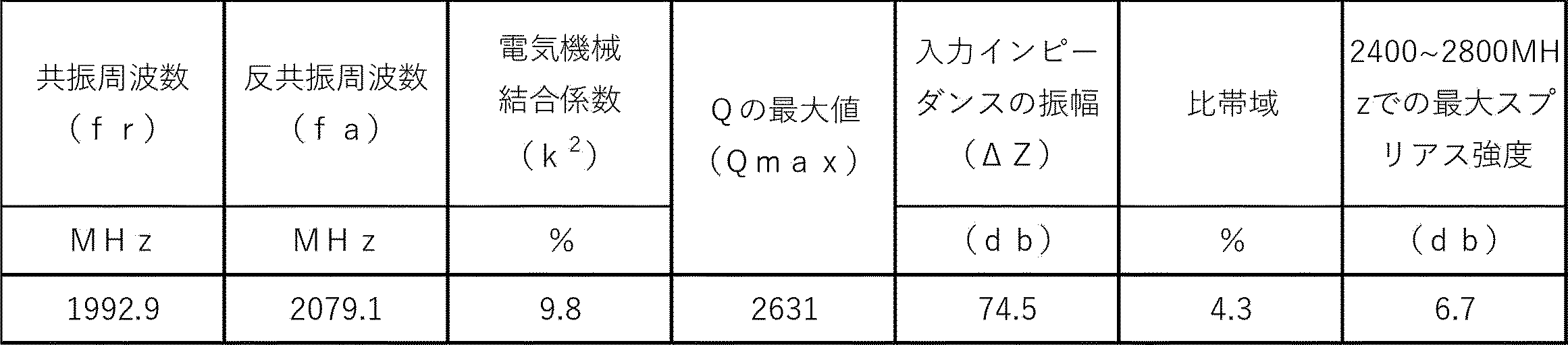
- Table 1 also shows the resonant frequency (fr), anti-resonant frequency (fa), electromechanical coupling coefficient (k 2 ), maximum Q (Qmax), input impedance amplitude ( ⁇ Z), fractional bandwidth, and spurious intensity between 2400 and 2800 MHz of the SAW resonator.
- an iron-containing lithium tantalate (LT) piezoelectric single crystal thin film substrate bonded to a silicon substrate with a one-port SAW resonator pattern created in the same manner as in Example 1 was placed on a hot plate heated to 350°C for 10 minutes, then placed on a cooling plate at room temperature to cool, and the electrical characteristics of the one-port SAW resonator were measured again with a network analyzer. The resulting characteristics were the same as those in Table 2. Furthermore, this 350°C hot plate heating, cooling, and measurement were repeated for a total of four hours with a cumulative heating time of 350°C hot plate, and the electrical characteristics of the one-port SAW resonator after each cumulative heating time did not change from those in Table 2.
- LT iron-containing lithium tantalate
- the amount of lithium in the melt was adjusted to a composition in which it was reduced based on the amount of lithium contained in the lithium tantalate crystal of the congruent composition, and an iron-substituted lithium tantalate crystal was grown from the melt of the adjusted composition.
- a 6-inch iron-containing 42° Y-cut lithium tantalate (LT) substrate was prepared by adding iron in an amount such that the iron content in the iron-substituted lithium tantalate crystal was 95 ppm by mass.
- the volume resistivity of the iron-containing 42° Y-cut lithium tantalate (LT) substrate was adjusted to 2.2 ⁇ 10 ⁇ cm by reduction treatment.
- the silicon substrate on which the polysilicon layer was formed and the iron-containing LT substrate having a 0.4 ⁇ m thick SiO 1.7 intervening layer were subjected to a surface activation treatment by plasma treatment.Furthermore, the silicon substrate on which the polysilicon layer was formed and the iron-containing LT substrate were bonded together with the 0.4 ⁇ m thick SiO 1.7 intervening layer to form a bonded body.
- the bonded body was heat-treated at 350° C. in nitrogen.
- the heat-treated bonded body was heated to 110° C., and a wedge was driven into one end of the ion-implanted portion of the iron-containing lithium tantalate (LT) substrate to separate it into the iron-containing lithium tantalate (LT) piezoelectric single crystal thin film layer bonded to the support substrate and the remaining iron-containing lithium tantalate (LT) substrate.
- the thickness of the iron-containing lithium tantalate (LT) piezoelectric single crystal thin film layer bonded to the silicon substrate after separation was measured by a spectrophotometer and found to be 0.52 ⁇ m.
- the composite substrate consisting of the iron-containing lithium tantalate (LT) piezoelectric single crystal thin film bonded to the silicon substrate was heated at 500° C. for 6 hours.
- the surface layer of the iron-containing lithium tantalate (LT) piezoelectric single crystal thin film of the composite substrate was polished by 20 nm, and the thickness of the iron-containing lithium tantalate (LT) piezoelectric single crystal thin film layer bonded to the silicon substrate was measured using a spectrophotometer, and found to be 0.5 ⁇ m.
- the amount of Li in the intermediate layer (SiO 1.7 layer) of the composite substrate manufactured by the above method was measured by secondary ion mass spectrometry (SIMS), and the maximum amount of Li in the SiO 1.7 layer was 2 ⁇ 10 17 atom/cm 3.
- the composition ratio of the intermediate layer (SiO 1.7 layer) was determined by X-ray photoelectron spectroscopy (XPS).
- the density of the intermediate layer (SiO 1.7 layer) was determined by XPS (X-ray photoelectron spectroscopy) and was found to be 2240 g/cm 3.
- the longitudinal wave sound velocity and attenuation of the intermediate layer (SiO 1.7 layer) were also determined by the Brillouin oscillation method. As a result, the longitudinal wave sound velocity of the intermediate layer (SiO 1.7 layer) was 6325 m/s, and the sound attenuation rate was 10.8 ⁇ 10 -2 (nm -1 ⁇ THz -2 ) at 55 GHz.
- the shear wave acoustic velocity of the intermediate layer (SiO 2 1.7 layer) alone was determined by a combination of a linear convergent beam ultrasonic microscope and finite element analysis, and was found to be 3960 m/s.
- an Al film was sputtered to a thickness of 0.14 ⁇ m on the surface of the composite substrate obtained above, and a resist was applied, followed by forming a resist pattern with a line width of about 0.5 ⁇ m by i-line exposure. Then, the Al was etched by dry etching to form the first layer of a one-port SAW resonator. Furthermore, a second layer pad portion of an Al film having a thickness of 0.6 ⁇ m was formed on the above composite substrate by a lift-off method. At this time, the wavelength of the surface acoustic wave was 2 ⁇ m, and the thickness of the intermediate layer (SiO 1.7 layer) was 0.2 wavelengths.
- the electrical characteristics of the one-port SAW resonator on the lithium iron tantalate (LT) piezoelectric single crystal thin film substrate bonded to the silicon substrate prepared above were measured using a network analyzer.
- the obtained SAW resonance waveform (input impedance (Zin) and Q value) is shown in Figure 9.
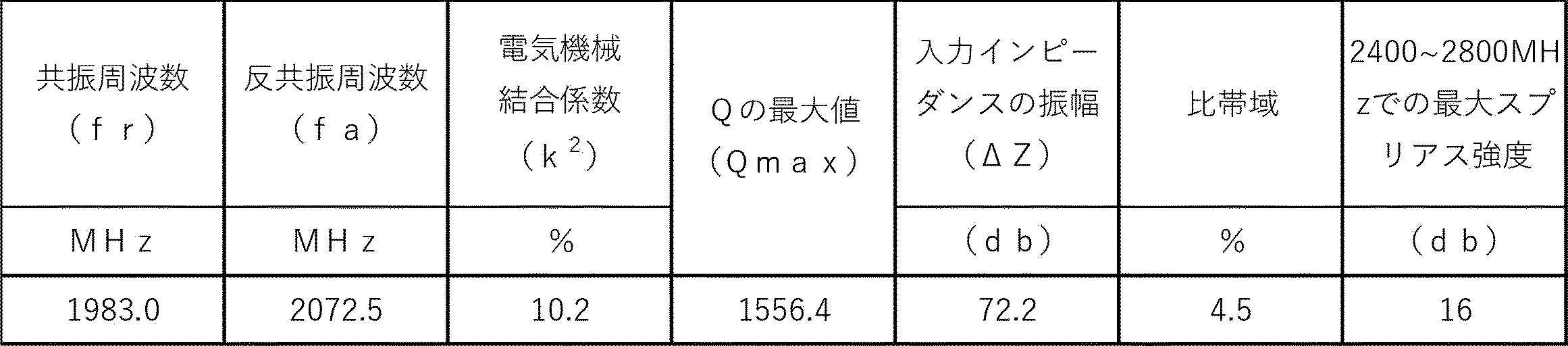
- Table 3 also shows the resonant frequency (fr), anti-resonant frequency (fa), electromechanical coupling coefficient (k 2 ), maximum Q (Qmax), input impedance amplitude ( ⁇ Z), fractional bandwidth, and spurious intensity between 2400 and 2800 MHz of the SAW resonator.
- the iron-containing lithium tantalate (LT) piezoelectric single crystal thin film substrate bonded to the silicon substrate with the one-port SAW resonator pattern created above was placed on a hot plate heated to 350°C for 10 minutes, then placed on a cooling plate at room temperature to cool, and the electrical characteristics of the one-port SAW resonator were measured again with a network analyzer.
- the resulting characteristics were the same as those in Table 3.
- this 350°C hot plate heating, cooling, and measurement was repeated for a total of four hours of cumulative heating at 350°C, and the electrical characteristics of the one-port SAW resonator after each cumulative heating time did not change from those in Table 3.
- an iron-free lithium tantalate crystal was grown on the lithium tantalate crystal of the congruent composition.
- a 6-inch iron-free lithium tantalate (LT) substrate with a 42° Y-cut was prepared by processing an iron-free lithium tantalate crystal.
- the volume resistivity of the iron-free lithium tantalate (LT) substrate was adjusted to 2.2 ⁇ 10 ⁇ cm by reduction treatment.
- a 0.4 ⁇ m-thick intermediate layer having a composition of SiO 2 was formed by CVD on the ion-implanted surface of a 6-inch iron-free lithium tantalate (LT) substrate.
- LT lithium tantalate
- the silicon substrate on which the polysilicon layer was formed and the iron-free LT substrate having a 0.4 ⁇ m thick SiO 2 intervening layer were subjected to a surface activation treatment by plasma treatment. Furthermore, the silicon substrate on which the polysilicon layer was formed and the iron-free LT substrate were bonded together with the 0.4 ⁇ m thick SiO 2 intervening layer to form a bonded body.
- the surface of the bonded body (bonded substrate) was removed by grinding and polishing.
- the thickness of the iron-free lithium tantalate (LT) piezoelectric single crystal thin film layer bonded to the thinned silicon substrate was measured by a spectrophotometer and found to be 0.5 ⁇ m.
- the amount of Li in the intermediate layer ( SiO2 layer) of the composite substrate manufactured by the above method was measured by secondary ion mass spectrometry (SIMS), and the maximum amount of Li in the SiO2 layer was 5 x 10¹⁹ atom/ cm3 .
- the composition ratio of the intermediate layer ( SiO2 layer) was determined by X-ray photoelectron spectroscopy (XPS).
- the LT layer of the composite substrate manufactured by the above method was removed, and the density of the intermediate layer (SiO 2 layer) was obtained by X-ray reflectometry (XRR).
- the density of the intermediate layer (SiO 2 layer) was 2100 g/cm 3.
- the LT layer of the composite substrate was removed, and the longitudinal wave sound velocity and attenuation of the intermediate layer (SiO 2 layer) were obtained by the Brillouin oscillation method.
- the longitudinal wave sound velocity of the intermediate layer (SiO 2 layer) was 5400 m/s, and the sound attenuation rate was 5 ⁇ 10 ⁇ 1 (nm ⁇ 1 ⁇ THz ⁇ 2 ) at 55 GHz.
- the shear wave acoustic velocity of the SiO 2 layer alone, which is the intermediate layer was determined by combining the linear convergent beam ultrasonic microscope and finite element analysis described above, and was found to be 3150 m/s.
- the obtained SAW resonance waveform (input impedance (Zin) and Q value) is shown in Figure 10.
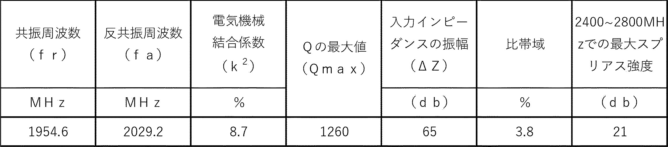
- the resonant frequency (fr), anti-resonant frequency (fa), electromechanical coupling coefficient ( k2 ), maximum Q (Qmax), input impedance amplitude ( ⁇ Z), band ratio, and spurious intensity between 2400 and 2800 MHz of the SAW resonator are shown in Table 4.
- the wavelength of the surface acoustic wave is 2 ⁇ m
- the thickness of the intermediate layer ( SiO2 layer) is 0.2 wavelengths.
- the iron-free lithium tantalate (LT) piezoelectric single crystal thin film substrate bonded to the silicon substrate with the one-port SAW resonator pattern created above was placed on a hot plate heated to 350°C for 10 minutes, then placed on a cooling plate at room temperature to cool, and the electrical characteristics of the one-port SAW resonator were measured again using a network analyzer.
- the results were the same as those in Table 4.
- the electromechanical coupling coefficient ( k2 ) began to decrease from the value in Table 3 when the cumulative heating time reached about one hour, and the electromechanical coupling coefficient ( k2 ) had decreased to 5% after a cumulative heating time of four hours.
Landscapes
- Physics & Mathematics (AREA)
- Acoustics & Sound (AREA)
- Chemical & Material Sciences (AREA)
- Engineering & Computer Science (AREA)
- Ceramic Engineering (AREA)
- Materials Engineering (AREA)
- Surface Acoustic Wave Elements And Circuit Networks Thereof (AREA)
Abstract
Description
[1]圧電単結晶薄膜と、支持基板と、前記圧電単結晶薄膜と前記支持基板の間に設けられた少なくとも1層の介在層と、を備える複合基板であって、前記介在層は前記圧電単結晶薄膜と接しており、前記介在層の合計厚みは、表面弾性波の波長の2倍の厚み以下であり、かつブリリュアン振動法により40GHz~60GHzの周波数で算出した前記介在層の縦波の減衰が8×10⁻²(nm-1・THz-2)以下である表面弾性波デバイス用複合基板。
[2]前記介在層の横波の音速は、前記圧電単結晶薄膜の遅い横波の音速より速い[1]に記載の表面弾性波デバイス用複合基板。
[3]前記圧電単結晶薄膜は、鉄を120ppm以下含み、前記圧電単結晶薄膜の体積抵抗率は2×10¹¹Ω・cm以下である[1]又は[2]に記載の表面弾性波デバイス用複合基板。
[4]前記介在層は、SiOx(1.8<x<2.05)、及びSiOyNz(0.02<z/(y+z)<0.1)のいずれかである[1]~[3]のいずれか1つに記載の表面弾性波デバイス用複合基板。
[5]前記圧電単結晶薄膜の主成分が、タンタル酸リチウムもしくはニオブ酸リチウムである[1]~[4]のいずれか1つに記載の表面弾性波デバイス用複合基板。
[6]前記支持基板が、シリコン基板、サファイア基板、アルミナ基板、炭化ケイ素基板、窒化アルミニウム基板、窒化ケイ素基板、及び水晶基板のいずれかである[1]~[5]のいずれか1つに記載の表面弾性波デバイス用複合基板。
[7]前記支持基板は、Si単結晶とSi単結晶上に形成したポリシリコン層からなる[1]~[5]のいずれか1つに記載の表面弾性波デバイス用複合基板。
[8]前記介在層中のLiイオンの含有量が、1×10¹⁷atom/cm3以下である[1]~[7]のいずれか1つに記載の表面弾性波デバイス用複合基板
本発明の表面弾性波デバイス用複合基板は、圧電単結晶薄膜と、支持基板と、圧電単結晶薄膜と支持基板の間に設けられた少なくとも1層の介在層と、を備える複合基板であって、介在層は圧電単結晶薄膜と接しており、介在層の合計厚みは、表面弾性波の波長の2倍の厚み以下であり、かつブリリュアン振動法により40GHz~60GHzの周波数で算出した介在層の縦波の減衰が8×10⁻²(nm-1・THz-2)以下である。
本発明の一実施形態における表面弾性波デバイス複合基板における圧電単結晶薄膜は、圧電体膜として使用することができれば特に制限されないが、主成分が、タンタル酸リチウム(LiTaO3:LT)、又は、ニオブ酸リチウム(LiNbO3:LN)であることが好ましい。圧電単結晶薄膜の主成分を上記成分とすることで、電気機械結合が大きな弾性波デバイスとすることができる。
なお、本願発明において、圧電単結晶薄膜の主成分が、タンタル酸リチウム、又はニオブ酸リチウムであるとは、圧電単結晶薄膜を構成する成分のうち、50質量%以上が、タンタル酸リチウム、又はニオブ酸リチウムであることをいう。また、圧電単結晶薄膜の成分として、タンタル酸リチウム及びニオブ酸リチウム以外の成分として、鉄,マグネシウム等を含有することができる。
本発明の一実施形態における表面弾性波デバイス複合基板における支持基板は、シリコン基板、サファイア基板、アルミナ基板、炭化ケイ素基板、窒化アルミニウム基板、窒化ケイ素基板、水晶基板のいずれかを用いることができる。
支持基板として、上記の基板を用いた表面弾性波デバイス用複合基板を用いて製造された表面弾性波共振子は、Q値が高く、帯域外のスプリアスがさらに抑制され、さらに、温度特性が優れた表面弾性波デバイスを得ることができる。
支持基板として、ポリシリコン層の厚みを適宜調整することで、帯域外のスプリアスをさらに抑制することができる。
ポリシリコン層の厚みは、0.2μm以上2μm以下であることが好ましく、0.5μm以上1.9μm以下であることがより好ましく、0.5μm以上1.2μm以下であることがさらに好ましい。
本発明の表面弾性波デバイス用複合基板は、上記の圧電単結晶薄膜と、支持基板との間に介在層を備え、介在層は、圧電単結晶薄膜と接して設けられている。本発明の一実施形態における表面弾性波デバイス複合基板における介在層は、SiOx(1.8<x<2.05)、及びSiOyNz(0.02<z/(y+z)<0.1)のいずれかであることが好ましい。
また、本発明の表面弾性波デバイス用複合基板は、少なくとも1層の介在層を備えている。介在層は1層であっても良く、2層以上であってもよく、2層以上の場合は、各層を同じ材料で構成しても良く、異なる材料で構成しても良い。
介在層の縦波の音波減衰が大きい場合は、介在層内に弾性波がトラップされやすくなる。この場合、本発明の表面弾性波デバイス用複合基板からなる表面弾性波共振子は、帯域外のスプリアスが大きくなる問題が生じる。介在層の縦波の減衰を8×10⁻²(nm-1・THz-2)以下とすることで、表面弾性波共振子のQ値が高く、帯域外のスプリアスをさらに抑制することができる。介在層の縦波の減衰は、2×10⁻²(nm-1・THz-2)以下であることが好ましく、0.5×10⁻²(nm-1・THz-2)以下であることがより好ましい。
介在層をSiO1.85、あるいはSiO1.94N0.06とし、圧電単結晶薄膜をLiTaO3とすることで、介在層の横波の音速が、圧電単結晶薄膜の遅い横波の音速より速くすることができる。
また、薄膜の密度(ρ)はXPS(X線光電子分光法)によって求めたところ、2300kg/m3であった。図1に示すブリリュアンスペクトルの前半部位は、薄膜内の超音波(縦波)による回折による反射光強度を示している。薄膜内の超音波(縦波)による反射光のみをフーリエ変換すると、図2に示す薄膜内の超音波(縦波)の周波数が得られる。図2から前記の薄膜内の超音波(縦波)の周波数(f)は、54.5GHzと算出できる。
vl=f×λ/(2×n) ・・・・・・式(1)
式(1)により求めた図2に示す薄膜内の超音波(縦波)の音速は6325m/sであった。また、薄膜の弾性定数C11はvl=√(C11/ρ)より算出でき、薄膜の弾性定数C11は92GPaとなった。
まず、例えば、上述したTatsuya Omori1, Kensuke Sakamoto, Satoshi Suzuki , Jun-ichi Kushibiki, Satoru Matsuda , and Ken-ya Hashimoto , “Characterization of Elastic Properties of SiO2 Thin Films by Ultrasonic Microscopy”,に記載されている直線収束ビーム超音波顕微鏡により、薄膜のLSAW音速を、周波数を160MHz~275MHzと変化させて、薄膜厚を超音波の波長で規格化した値(薄膜厚/波長)の異存性を求めた。関係図を図3に示す。
また、一例として弾性波波長が18μmの場合の有限要素法による計算モデルにおいて弾性波がSiO1.7薄膜/(111)Si基板構成の薄膜表層にエネルギーが集中している波動の変位分布計算結果例を図4に示した。
A=A0・exp(-β・f2・d) ・・・・・・式(2)
図2の場合、A0は0.03、Aは0.004であった。前記より減衰定数βを式(3)より求める。
β=-1/(f2・d)・In(A/A0) ・・・・式(3)
図2の場合 βは 10.8×10⁻²(nm-1・THz-2)であった。
介在層の縦波の音波減衰が大きい場合は、介在層内に弾性波がトラップされやすくなる。この場合、表面弾性波デバイス用複合基板からなる表面弾性波共振子は、帯域外のスプリアスが大きくなる問題が生じることを確認した。
一方、本願発明による介在層が高音速でかつ縦波の減衰が少ないと、介在層に極端に弾性波が集中することができずに、圧電単結晶薄膜に波動エネルギーを集中させることができる。このため、本願発明の表面弾性波デバイス用複合基板を用いた表面弾性波共振子のQ値が高く、帯域外のスプリアスがさらに抑圧され好ましい。
直径150mmの(111)方位の高抵抗シリコン基板の表層にポリシリコン層を1.7μm形成した。
鉄の添加量を、鉄置換タンタル酸リチウム結晶中の鉄の含有量が95質量ppmになるように調整して得られた6inchの鉄含有42°Yカットのタンタル酸リチウム(LT)基板を準備した。鉄含有42°Yカットのタンタル酸リチウム(LT)基板は、還元処理を施すことにより体積抵抗率を2.2×10¹⁰Ω・cmに調整した。
続いて、水素分子イオンを注入した6inchの鉄含有タンタル酸リチウム(LT)基板イオン注入面に0.4μm厚の組成がSiO1.85である介在層をCVD法により形成した。
続いて、上記のポリシリコン層を形成したシリコン基板と、0.4μm厚のSiO1.85を用いた介在層を有する鉄含有LT基板をプラズマ処理により表面活性化処理を行った。さらに、ポリシリコン層を形成したシリコン基板と、0.4μm厚のSiO1.85を用いた介在層を介在させて鉄含有LT基板と、を貼り合せて接合体とした。
分離後のシリコン基板に接合された鉄含有タンタル酸リチウム(LT)圧電単結晶薄膜層の厚みを分光光度計により測定したところ、0.52μmの厚みであった。次に、このシリコン基板に接合された鉄含有タンタル酸リチウム(LT)圧電単結晶薄膜層からなる複合基板を500℃で6時間加熱した。
図5は、上記の方法で製造した実施例1の複合基板の断面TEM観察写真例を示す図であり、図5(b)は図5(a)の一部をさらに拡大した写真である。
また、介在層(SiO1.85層)単体の横波音速を直線収束ビーム超音波顕微鏡と有限要素法解析を組み合わせて求めたところ、介在層(SiO1.85層)単体の横波音速は3850m/sであった。
さらに、上記の複合基板に、リフトオフ法によりAl膜0.6μm厚の2層目のパッド部を形成した。図6に、表面にAl微細電極を形成した複合基板を示す。
また、SAW共振子の共振周波数(fr)、反共振周波数(fa),電気機械結合係数(k2)、Qの最大値(Qmax)、入力インピーダンスの振幅(ΔZ)、比帯域の値(比帯域=(反共振周波数-共振周波数)/共振周波数)、2400~2800MHz間のスプリアス強度を表1に示す。

実施例1において0.4μm厚で組成がSiO1.85である介在層の代わりに、0.3μm厚で組成がSiO1.94N0.06である介在層を用いた以外は実施例1と同様にしてシリコン基板に接合された鉄含有タンタル酸リチウム(LT)圧電単結晶薄膜からなる複合基板を作成した。
また、介在層であるSiO1.94N0.06層単体の横波音速を、前述した直線収束ビーム超音波顕微鏡と有限要素法解析を組み合わせて求めたところ、SiO1.94N0.06層単体の横波音速は3750m/sであった。
また、SAW共振子の共振周波数(fr)、反共振周波数(fa),電気機械結合係数(k2)、Qの最大値(Qmax)、入力インピーダンスの振幅(ΔZ)、比帯域の値、2400~2800MHz間のスプリアス強度を表1に示す。
直径150mmの(111)方位の高抵抗シリコン基板の表層にポリシリコン層を1.7μm形成した。
鉄の添加量を、鉄置換タンタル酸リチウム結晶中の鉄の含有量が95質量ppmになるように添加して得られた6inchの鉄含有42°Yカットのタンタル酸リチウム(LT)基板を準備した。鉄含有42°Yカットのタンタル酸リチウム(LT)基板は、還元処理を施すことにより体積抵抗率を2.2×10¹⁰Ω・cmに調整した。
続いて、水素分子イオンを注入した6inchの鉄含有タンタル酸リチウム(LT)基板イオン注入面に0.4μm厚の組成がSiO1.7である介在層をCVD法により形成した。
続いて、上記のポリシリコン層を形成したシリコン基板と、0.4μm厚のSiO1.7を用いた介在層を有する鉄含有LT基板をプラズマ処理により表面活性化処理を行った。さらに、上記のポリシリコン層を形成したシリコン基板と0.4μm厚のSiO1.7を用いた介在層を介在させて鉄含有LT基板を貼り合せて接合体とした。
分離後のシリコン基板に接合された鉄含有タンタル酸リチウム(LT)圧電単結晶薄膜層の厚みを分光光度計により測定したところ、0.52μmの厚みであった。次にこのシリコン基板に接合された鉄含有タンタル酸リチウム(LT)圧電単結晶薄膜からなる複合基板を500℃で6時間加熱した。
また、介在層(SiO1.7層)単体の横波音速を直線収束ビーム超音波顕微鏡と有限要素法解析を組み合わせて求めたところ、介在層(SiO1.7層)単体の横波音速は3960m/sであった。
さらに、上記の複合基板に、リフトオフ法によりAl膜0.6μm厚の2層目のパッド部を形成した。この時、弾性表面波の波長は2μmであり、介在層(SiO1.7層)の厚みは0.2波長である。
また、SAW共振子の共振周波数(fr)、反共振周波数(fa),電気機械結合係数(k2)、Qの最大値(Qmax)、入力インピーダンスの振幅(ΔZ)、比帯域の値、2400~2800MHz間のスプリアス強度を表3に示す。
直径150mmの高抵抗シリコン基板の表層にポリシリコン層を1.7μm形成した。
鉄非含有のタンタル酸リチウム結晶を加工し、6inchの鉄非含有42°Yカットのタンタル酸リチウム(LT)基板を準備した。鉄非含有42°Yカットのタンタル酸リチウム(LT)基板は、還元処理を施すことにより体積抵抗率を2.2×10Ω・cmに調整した。
続いて、上記のポリシリコン層を形成したシリコン基板と、0.4μm厚のSiO2を用いた介在層を有する鉄非含有LT基板をプラズマ処理により表面活性化処理を行った。さらに、上記のポリシリコン層を形成したシリコン基板と0.4μm厚のSiO2を用いた介在層を介在させて鉄非含有LT基板を貼り合せて接合体とした。
薄化後のシリコン基板に接合された鉄非含有タンタル酸リチウム(LT)圧電単結晶薄膜層の厚みを分光光度計により測定したところ、0.5μmの厚みであった。
また、介在層であるSiO2層単体の横波音速を、前述した直線収束ビーム超音波顕微鏡と有限要素法解析を組み合わせて求めたところ、前記のSiO2層単体の横波音速は3150m/sであった。
また、SAW共振子の共振周波数(fr)、反共振周波数(fa),電気機械結合係数(k2)、Qの最大値(Qmax)、入力インピーダンスの振幅(ΔZ)、比帯域の値、2400~2800MHz間のスプリアス強度を表4に示す。この時、弾性表面波の波長は2μmであり、介在層(SiO2層)の厚みは0.2波長である。
Claims (8)
- 圧電単結晶薄膜と、支持基板と、前記圧電単結晶薄膜と前記支持基板の間に設けられた少なくとも1層の介在層と、を備える複合基板であって、
前記介在層は前記圧電単結晶薄膜と接しており、前記介在層の合計厚みは、表面弾性波の波長の2倍の厚み以下であり、かつブリリュアン振動法により40GHz~60GHzの周波数で算出した前記介在層の縦波の減衰が8×10⁻²(nm-1・THz-2)以下である表面弾性波デバイス用複合基板。 - 前記介在層の横波の音速は、前記圧電単結晶薄膜の遅い横波の音速より速い請求項1に記載の表面弾性波デバイス用複合基板。
- 前記圧電単結晶薄膜は、鉄を120ppm以下含み、
前記圧電単結晶薄膜の体積抵抗率は2×10¹¹Ω・cm以下である請求項1又は2に記載の表面弾性波デバイス用複合基板。 - 前記介在層は、SiOx(1.8<x<2.05)、及びSiOyNz(0.02<z/(y+z)<0.1)のいずれかである請求項1又は2に記載の表面弾性波デバイス用複合基板。
- 前記圧電単結晶薄膜の主成分が、タンタル酸リチウムもしくはニオブ酸リチウムである請求項1又は2に記載の表面弾性波デバイス用複合基板。
- 前記支持基板が、シリコン基板、サファイア基板、アルミナ基板、炭化ケイ素基板、窒化アルミニウム基板、窒化ケイ素基板、及び水晶基板のいずれかである請求項1又は2に記載の表面弾性波デバイス用複合基板。
- 前記支持基板は、Si単結晶とSi単結晶上に形成したポリシリコン層からなる請求項1又は2に記載の表面弾性波デバイス用複合基板。
- 前記介在層中のLiイオンの含有量が、1×10¹⁷atom/cm3以下である請求項1又は2に記載の表面弾性波デバイス用複合基板。
Priority Applications (3)
| Application Number | Priority Date | Filing Date | Title |
|---|---|---|---|
| KR1020257036969A KR20260009285A (ko) | 2023-05-09 | 2024-04-01 | 표면 탄성파 디바이스용 복합 기판 |
| CN202480030773.6A CN121079897A (zh) | 2023-05-09 | 2024-04-01 | 表面弹性波器件用复合基板 |
| EP24803307.8A EP4712346A1 (en) | 2023-05-09 | 2024-04-01 | Composite substrate for surface acoustic wave devices |
Applications Claiming Priority (2)
| Application Number | Priority Date | Filing Date | Title |
|---|---|---|---|
| JP2023077370A JP7754878B2 (ja) | 2023-05-09 | 2023-05-09 | 表面弾性波デバイス用複合基板 |
| JP2023-077370 | 2023-05-09 |
Publications (1)
| Publication Number | Publication Date |
|---|---|
| WO2024232192A1 true WO2024232192A1 (ja) | 2024-11-14 |
Family
ID=93430191
Family Applications (1)
| Application Number | Title | Priority Date | Filing Date |
|---|---|---|---|
| PCT/JP2024/013466 Ceased WO2024232192A1 (ja) | 2023-05-09 | 2024-04-01 | 表面弾性波デバイス用複合基板 |
Country Status (5)
| Country | Link |
|---|---|
| EP (1) | EP4712346A1 (ja) |
| JP (1) | JP7754878B2 (ja) |
| KR (1) | KR20260009285A (ja) |
| CN (1) | CN121079897A (ja) |
| WO (1) | WO2024232192A1 (ja) |
Citations (5)
| Publication number | Priority date | Publication date | Assignee | Title |
|---|---|---|---|---|
| JP5713025B2 (ja) | 2010-12-24 | 2015-05-07 | 株式会社村田製作所 | 弾性波装置及びその製造方法 |
| JP5861789B2 (ja) | 2011-09-30 | 2016-02-16 | 株式会社村田製作所 | 弾性波装置 |
| JP2021005785A (ja) * | 2019-06-26 | 2021-01-14 | 信越化学工業株式会社 | 表面弾性波デバイス用複合基板及びその製造方法 |
| JP2021180465A (ja) * | 2020-05-15 | 2021-11-18 | 信越化学工業株式会社 | 表面弾性波デバイス用複合基板及びその製造方法 |
| CN113872557A (zh) * | 2021-09-29 | 2021-12-31 | 北京超材信息科技有限公司 | 用于声表面波器件的复合衬底及制造方法、声表面波器件 |
-
2023
- 2023-05-09 JP JP2023077370A patent/JP7754878B2/ja active Active
-
2024
- 2024-04-01 KR KR1020257036969A patent/KR20260009285A/ko active Pending
- 2024-04-01 CN CN202480030773.6A patent/CN121079897A/zh active Pending
- 2024-04-01 EP EP24803307.8A patent/EP4712346A1/en active Pending
- 2024-04-01 WO PCT/JP2024/013466 patent/WO2024232192A1/ja not_active Ceased
Patent Citations (5)
| Publication number | Priority date | Publication date | Assignee | Title |
|---|---|---|---|---|
| JP5713025B2 (ja) | 2010-12-24 | 2015-05-07 | 株式会社村田製作所 | 弾性波装置及びその製造方法 |
| JP5861789B2 (ja) | 2011-09-30 | 2016-02-16 | 株式会社村田製作所 | 弾性波装置 |
| JP2021005785A (ja) * | 2019-06-26 | 2021-01-14 | 信越化学工業株式会社 | 表面弾性波デバイス用複合基板及びその製造方法 |
| JP2021180465A (ja) * | 2020-05-15 | 2021-11-18 | 信越化学工業株式会社 | 表面弾性波デバイス用複合基板及びその製造方法 |
| CN113872557A (zh) * | 2021-09-29 | 2021-12-31 | 北京超材信息科技有限公司 | 用于声表面波器件的复合衬底及制造方法、声表面波器件 |
Non-Patent Citations (2)
| Title |
|---|
| See also references of EP4712346A1 |
| TATSUYA OMORI1KENSUKE SAKAMOTOSATOSHI SUZUKIJUN-ICHI KUSHIBIKISATORU MATSUDAKEN-YA HASHIMOTO, CHARACTERIZATION OF ELASTIC PROPERTIES OF SIO THIN FILMS BY ULTRASONIC MICROSCOPY |
Also Published As
| Publication number | Publication date |
|---|---|
| CN121079897A (zh) | 2025-12-05 |
| KR20260009285A (ko) | 2026-01-19 |
| JP2024162125A (ja) | 2024-11-21 |
| EP4712346A1 (en) | 2026-03-18 |
| JP7754878B2 (ja) | 2025-10-15 |
Similar Documents
| Publication | Publication Date | Title |
|---|---|---|
| JP7317068B2 (ja) | 石英基板上に圧電層を含む弾性表面波デバイス及びその製造方法 | |
| JP6250856B1 (ja) | 表面弾性波デバイス用複合基板及びその製造方法とこの複合基板を用いた表面弾性波デバイス | |
| TWI884125B (zh) | 聲波裝置、製造所述聲波裝置的方法及包括所述聲波裝置的濾波器 | |
| JP7051690B2 (ja) | スプリアスモード除去をもたらす誘導表面弾性波デバイス | |
| KR102519924B1 (ko) | 탄탈산리튬 단결정 기판 및 이것의 접합 기판과 이 제조법 및 이 기판을 사용한 탄성 표면파 디바이스 | |
| JP5797979B2 (ja) | 弾性波デバイス | |
| Nakahata et al. | SAW devices on diamond | |
| WO2018066653A1 (ja) | 複合基板及び複合基板の製造方法 | |
| JP7163249B2 (ja) | 表面弾性波デバイス用複合基板及びその製造方法 | |
| TW201927558A (zh) | 鉭酸鋰單晶體基板、黏合基板、黏合基板之製造方法、以及使用黏合基板之表面聲波器件 | |
| Naumenko | Multilayered structures using thin plates of LiTaO3 for acoustic wave resonators with high quality factor | |
| JP6646058B2 (ja) | 接合基板及びその製造方法とこの接合基板を用いた弾性表面波デバイス | |
| CN107404302A (zh) | 具有用于抑制假信号响应的吸收层的复合表面声波saw装置 | |
| KR20200040827A (ko) | 압전성 재료 기판과 지지 기판의 접합체 및 탄성파 소자 | |
| WO2007037457A9 (ja) | 弾性表面波デバイス、モジュール装置、発振回路および弾性表面波デバイスの製造方法 | |
| JP7754878B2 (ja) | 表面弾性波デバイス用複合基板 | |
| Onishi et al. | A novel temperature compensation method for SAW devices using direct bonding techniques | |
| Yang et al. | Application of Periodically Slotted SiO 2 to Layered SAW Structure for Manipulation of SAW Slowness Curve | |
| JP6432944B2 (ja) | 接合基板及びこれを用いた弾性表面波デバイス | |
| Tanakura et al. | 3P3-4 High order mode HAL SAW quartz resonator using silicon or sapphire as support substrate | |
| Fujii et al. | P5I-4 Diamond Saw Resonators With SiO2/ZnO/IDT/ZnO/Diamond Structure | |
| JP2020129762A (ja) | 複合基板の製造方法 |
Legal Events
| Date | Code | Title | Description |
|---|---|---|---|
| 121 | Ep: the epo has been informed by wipo that ep was designated in this application |
Ref document number: 24803307 Country of ref document: EP Kind code of ref document: A1 |
|
| WWE | Wipo information: entry into national phase |
Ref document number: 2024803307 Country of ref document: EP |
|
| NENP | Non-entry into the national phase |
Ref country code: DE |
|
| ENP | Entry into the national phase |
Ref document number: 2024803307 Country of ref document: EP Effective date: 20251209 |
|
| ENP | Entry into the national phase |
Ref document number: 2024803307 Country of ref document: EP Effective date: 20251209 |
|
| ENP | Entry into the national phase |
Ref document number: 2024803307 Country of ref document: EP Effective date: 20251209 |
|
| ENP | Entry into the national phase |
Ref document number: 2024803307 Country of ref document: EP Effective date: 20251209 |
|
| ENP | Entry into the national phase |
Ref document number: 2024803307 Country of ref document: EP Effective date: 20251209 |
|
| ENP | Entry into the national phase |
Ref document number: 2024803307 Country of ref document: EP Effective date: 20251209 |
|
| ENP | Entry into the national phase |
Ref document number: 2024803307 Country of ref document: EP Effective date: 20251209 |
|
| ENP | Entry into the national phase |
Ref document number: 2024803307 Country of ref document: EP Effective date: 20251209 |
|
| ENP | Entry into the national phase |
Ref document number: 2024803307 Country of ref document: EP Effective date: 20251209 |
|
| WWP | Wipo information: published in national office |
Ref document number: 2024803307 Country of ref document: EP |