WO2024225406A1 - 炭化珪素半導体装置 - Google Patents
炭化珪素半導体装置 Download PDFInfo
- Publication number
- WO2024225406A1 WO2024225406A1 PCT/JP2024/016351 JP2024016351W WO2024225406A1 WO 2024225406 A1 WO2024225406 A1 WO 2024225406A1 JP 2024016351 W JP2024016351 W JP 2024016351W WO 2024225406 A1 WO2024225406 A1 WO 2024225406A1
- Authority
- WO
- WIPO (PCT)
- Prior art keywords
- layer
- cell region
- region
- isolation
- trench
- Prior art date
- Legal status (The legal status is an assumption and is not a legal conclusion. Google has not performed a legal analysis and makes no representation as to the accuracy of the status listed.)
- Ceased
Links
Images





Classifications
-
- H—ELECTRICITY
- H10—SEMICONDUCTOR DEVICES; ELECTRIC SOLID-STATE DEVICES NOT OTHERWISE PROVIDED FOR
- H10D—INORGANIC ELECTRIC SEMICONDUCTOR DEVICES
- H10D62/00—Semiconductor bodies, or regions thereof, of devices having potential barriers
- H10D62/10—Shapes, relative sizes or dispositions of the regions of the semiconductor bodies; Shapes of the semiconductor bodies
- H10D62/102—Constructional design considerations for preventing surface leakage or controlling electric field concentration
- H10D62/103—Constructional design considerations for preventing surface leakage or controlling electric field concentration for increasing or controlling the breakdown voltage of reverse-biased devices
- H10D62/105—Constructional design considerations for preventing surface leakage or controlling electric field concentration for increasing or controlling the breakdown voltage of reverse-biased devices by having particular doping profiles, shapes or arrangements of PN junctions; by having supplementary regions, e.g. junction termination extension [JTE]
- H10D62/109—Reduced surface field [RESURF] PN junction structures
-
- H—ELECTRICITY
- H10—SEMICONDUCTOR DEVICES; ELECTRIC SOLID-STATE DEVICES NOT OTHERWISE PROVIDED FOR
- H10D—INORGANIC ELECTRIC SEMICONDUCTOR DEVICES
- H10D62/00—Semiconductor bodies, or regions thereof, of devices having potential barriers
- H10D62/10—Shapes, relative sizes or dispositions of the regions of the semiconductor bodies; Shapes of the semiconductor bodies
-
- H—ELECTRICITY
- H10—SEMICONDUCTOR DEVICES; ELECTRIC SOLID-STATE DEVICES NOT OTHERWISE PROVIDED FOR
- H10D—INORGANIC ELECTRIC SEMICONDUCTOR DEVICES
- H10D12/00—Bipolar devices controlled by the field effect, e.g. insulated-gate bipolar transistors [IGBT]
-
- H—ELECTRICITY
- H10—SEMICONDUCTOR DEVICES; ELECTRIC SOLID-STATE DEVICES NOT OTHERWISE PROVIDED FOR
- H10D—INORGANIC ELECTRIC SEMICONDUCTOR DEVICES
- H10D30/00—Field-effect transistors [FET]
- H10D30/01—Manufacture or treatment
- H10D30/021—Manufacture or treatment of FETs having insulated gates [IGFET]
-
- H—ELECTRICITY
- H10—SEMICONDUCTOR DEVICES; ELECTRIC SOLID-STATE DEVICES NOT OTHERWISE PROVIDED FOR
- H10D—INORGANIC ELECTRIC SEMICONDUCTOR DEVICES
- H10D30/00—Field-effect transistors [FET]
- H10D30/01—Manufacture or treatment
- H10D30/021—Manufacture or treatment of FETs having insulated gates [IGFET]
- H10D30/028—Manufacture or treatment of FETs having insulated gates [IGFET] of double-diffused metal oxide semiconductor [DMOS] FETs
- H10D30/0291—Manufacture or treatment of FETs having insulated gates [IGFET] of double-diffused metal oxide semiconductor [DMOS] FETs of vertical DMOS [VDMOS] FETs
- H10D30/0297—Manufacture or treatment of FETs having insulated gates [IGFET] of double-diffused metal oxide semiconductor [DMOS] FETs of vertical DMOS [VDMOS] FETs using recessing of the gate electrodes, e.g. to form trench gate electrodes
-
- H—ELECTRICITY
- H10—SEMICONDUCTOR DEVICES; ELECTRIC SOLID-STATE DEVICES NOT OTHERWISE PROVIDED FOR
- H10D—INORGANIC ELECTRIC SEMICONDUCTOR DEVICES
- H10D30/00—Field-effect transistors [FET]
- H10D30/60—Insulated-gate field-effect transistors [IGFET]
-
- H—ELECTRICITY
- H10—SEMICONDUCTOR DEVICES; ELECTRIC SOLID-STATE DEVICES NOT OTHERWISE PROVIDED FOR
- H10D—INORGANIC ELECTRIC SEMICONDUCTOR DEVICES
- H10D30/00—Field-effect transistors [FET]
- H10D30/60—Insulated-gate field-effect transistors [IGFET]
- H10D30/64—Double-diffused metal-oxide semiconductor [DMOS] FETs
- H10D30/65—Lateral DMOS [LDMOS] FETs
-
- H—ELECTRICITY
- H10—SEMICONDUCTOR DEVICES; ELECTRIC SOLID-STATE DEVICES NOT OTHERWISE PROVIDED FOR
- H10D—INORGANIC ELECTRIC SEMICONDUCTOR DEVICES
- H10D30/00—Field-effect transistors [FET]
- H10D30/60—Insulated-gate field-effect transistors [IGFET]
- H10D30/64—Double-diffused metal-oxide semiconductor [DMOS] FETs
- H10D30/66—Vertical DMOS [VDMOS] FETs
- H10D30/668—Vertical DMOS [VDMOS] FETs having trench gate electrodes, e.g. UMOS transistors
-
- H—ELECTRICITY
- H10—SEMICONDUCTOR DEVICES; ELECTRIC SOLID-STATE DEVICES NOT OTHERWISE PROVIDED FOR
- H10D—INORGANIC ELECTRIC SEMICONDUCTOR DEVICES
- H10D30/00—Field-effect transistors [FET]
- H10D30/60—Insulated-gate field-effect transistors [IGFET]
- H10D30/64—Double-diffused metal-oxide semiconductor [DMOS] FETs
- H10D30/66—Vertical DMOS [VDMOS] FETs
- H10D30/669—Vertical DMOS [VDMOS] FETs having voltage-sensing or current-sensing structures, e.g. emulator sections or overcurrent sensing cells
-
- H—ELECTRICITY
- H10—SEMICONDUCTOR DEVICES; ELECTRIC SOLID-STATE DEVICES NOT OTHERWISE PROVIDED FOR
- H10D—INORGANIC ELECTRIC SEMICONDUCTOR DEVICES
- H10D62/00—Semiconductor bodies, or regions thereof, of devices having potential barriers
- H10D62/01—Manufacture or treatment
- H10D62/051—Forming charge compensation regions, e.g. superjunctions
- H10D62/054—Forming charge compensation regions, e.g. superjunctions by high energy implantations in bulk semiconductor bodies, e.g. forming pillars
-
- H—ELECTRICITY
- H10—SEMICONDUCTOR DEVICES; ELECTRIC SOLID-STATE DEVICES NOT OTHERWISE PROVIDED FOR
- H10D—INORGANIC ELECTRIC SEMICONDUCTOR DEVICES
- H10D62/00—Semiconductor bodies, or regions thereof, of devices having potential barriers
- H10D62/10—Shapes, relative sizes or dispositions of the regions of the semiconductor bodies; Shapes of the semiconductor bodies
- H10D62/102—Constructional design considerations for preventing surface leakage or controlling electric field concentration
- H10D62/103—Constructional design considerations for preventing surface leakage or controlling electric field concentration for increasing or controlling the breakdown voltage of reverse-biased devices
- H10D62/105—Constructional design considerations for preventing surface leakage or controlling electric field concentration for increasing or controlling the breakdown voltage of reverse-biased devices by having particular doping profiles, shapes or arrangements of PN junctions; by having supplementary regions, e.g. junction termination extension [JTE]
- H10D62/106—Constructional design considerations for preventing surface leakage or controlling electric field concentration for increasing or controlling the breakdown voltage of reverse-biased devices by having particular doping profiles, shapes or arrangements of PN junctions; by having supplementary regions, e.g. junction termination extension [JTE] having supplementary regions doped oppositely to or in rectifying contact with regions of the semiconductor bodies, e.g. guard rings with PN or Schottky junctions
- H10D62/107—Buried supplementary regions, e.g. buried guard rings
-
- H—ELECTRICITY
- H10—SEMICONDUCTOR DEVICES; ELECTRIC SOLID-STATE DEVICES NOT OTHERWISE PROVIDED FOR
- H10D—INORGANIC ELECTRIC SEMICONDUCTOR DEVICES
- H10D62/00—Semiconductor bodies, or regions thereof, of devices having potential barriers
- H10D62/10—Shapes, relative sizes or dispositions of the regions of the semiconductor bodies; Shapes of the semiconductor bodies
- H10D62/124—Shapes, relative sizes or dispositions of the regions of semiconductor bodies or of junctions between the regions
- H10D62/126—Top-view geometrical layouts of the regions or the junctions
- H10D62/127—Top-view geometrical layouts of the regions or the junctions of cellular field-effect devices, e.g. multicellular DMOS transistors or IGBTs
-
- H—ELECTRICITY
- H10—SEMICONDUCTOR DEVICES; ELECTRIC SOLID-STATE DEVICES NOT OTHERWISE PROVIDED FOR
- H10D—INORGANIC ELECTRIC SEMICONDUCTOR DEVICES
- H10D62/00—Semiconductor bodies, or regions thereof, of devices having potential barriers
- H10D62/80—Semiconductor bodies, or regions thereof, of devices having potential barriers characterised by the materials
- H10D62/83—Semiconductor bodies, or regions thereof, of devices having potential barriers characterised by the materials being Group IV materials, e.g. B-doped Si or undoped Ge
- H10D62/832—Semiconductor bodies, or regions thereof, of devices having potential barriers characterised by the materials being Group IV materials, e.g. B-doped Si or undoped Ge being Group IV materials comprising two or more elements, e.g. SiGe
- H10D62/8325—Silicon carbide
-
- H—ELECTRICITY
- H10—SEMICONDUCTOR DEVICES; ELECTRIC SOLID-STATE DEVICES NOT OTHERWISE PROVIDED FOR
- H10W—GENERIC PACKAGES, INTERCONNECTIONS, CONNECTORS OR OTHER CONSTRUCTIONAL DETAILS OF DEVICES COVERED BY CLASS H10
- H10W10/00—Isolation regions in semiconductor bodies between components of integrated devices
-
- H—ELECTRICITY
- H10—SEMICONDUCTOR DEVICES; ELECTRIC SOLID-STATE DEVICES NOT OTHERWISE PROVIDED FOR
- H10W—GENERIC PACKAGES, INTERCONNECTIONS, CONNECTORS OR OTHER CONSTRUCTIONAL DETAILS OF DEVICES COVERED BY CLASS H10
- H10W10/00—Isolation regions in semiconductor bodies between components of integrated devices
- H10W10/01—Manufacture or treatment
Definitions
- This disclosure relates to a silicon carbide (hereinafter also referred to as SiC) semiconductor device having a trench gate structure semiconductor element in which a cell region includes a main cell region and a sense cell region.
- SiC silicon carbide
- Patent Document 1 proposes a SiC semiconductor device in which a cell region is provided with a main cell region and a sense cell region, and the current flowing through the main cell region is detected in the sense cell region.
- MOSFET elements of the same structure are formed in the main cell region and the sense cell region.
- an element isolation region is provided between the main cell region and the sense cell region, and the main cell region and the sense cell region are isolated from each other.
- the main cell region and the sense cell region have a trench gate structure, and a p-type protective layer is formed at the bottom of the trench in the trench gate structure, which spreads the depletion layer from the protective layer to the drift layer and reduces the electric field applied to the bottom of the trench.
- a single wide trench is formed in the element isolation region between the main cell region and the sense cell region, reaching the drift layer, and a p-type protective layer constituting an electric field relaxation layer is formed on both ends of the bottom of this trench, on the main cell region side and the sense cell side.
- a withstand voltage is obtained, while the electric field relaxation layer on the main cell region side and the electric field relaxation layer on the sense cell side are separated by a separation section, preventing a short circuit between the main cell region and the sense cell region through the electric field relaxation layer.
- An object of the present disclosure is to provide a SiC semiconductor device that can accurately isolate a main cell region and a sense cell region while ensuring a breakdown voltage in the isolation region.
- One aspect of the present disclosure is a SiC semiconductor device in which a semiconductor element having a trench gate structure is formed in a cell region including a main cell region and a sense cell region, and the main cell region and the sense cell region are electrically isolated by an element isolation region, the device having a substrate of a first conductivity type or a second conductivity type made of SiC, and a first impurity region of the first conductivity type formed on the surface of the substrate and having a lower impurity concentration than the substrate.
- the main cell region and the sense cell region include a JFET layer made of a first conductivity type SiC formed in a surface layer portion of the first impurity region and having a higher impurity concentration than the first impurity region, a deep layer made of a second conductivity type SiC formed in a surface layer portion of the first impurity region and arranged alternately with the JFET layer in a surface direction of the substrate, a base layer made of the second conductivity type SiC formed on the JFET layer and the deep layer, a gate insulating film formed on an inner wall surface of a plurality of gate trenches arranged deeper than the base layer and with one direction as a longitudinal direction, and a gate electrode formed on the gate insulating film in the gate trench, a trench gate structure having a second impurity region made of the first conductivity type SiC formed in contact with the trench gate structure in a surface layer portion of the base layer, a first electrode provided separately in each of the main cell region and the sense cell region, electrically connected to the second
- the element isolation region is disposed between the main cell region and the sense cell region, and a plurality of isolation trenches are formed deeper than the base layer, separating the base layer into the main cell region side and the sense cell region side. Furthermore, at the bottom of each of the plurality of isolation trenches, there is provided an isolation deep layer of the second conductivity type that is disposed apart from each other and is formed in contact with the bottom surface of the isolation trench.
- the base layer on the main cell region side and the base layer on the sense cell region side are separated by forming an isolation trench in the element isolation region.
- This allows the base layer on the main cell region side to be electrically isolated from the base layer on the sense cell region side.
- the provision of an isolation deep layer makes it possible to suppress the rise of the equipotential line between the main cell region and the sense cell region, and ensures the breakdown voltage. Since there are multiple isolation trenches and there is no need to make them wide as in the case of a single trench, the isolation trenches and the isolation deep layers formed at their bottoms are excellent, and each isolation deep layer is formed at an appropriate interval.
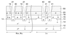
- FIG. 1 is a plan view of a SiC semiconductor device according to a first embodiment.
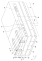
- FIG. 2 is a perspective cross-sectional view of an area RA in FIG. 1 as viewed from a direction II.
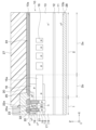
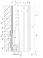
- FIG. 2 is a cross-sectional view taken along line III-III in FIG. 4 is a cross-sectional view taken along line IV-IV in FIG. 1.
- 2 is a cross-sectional view taken along line VV in FIG. 1.
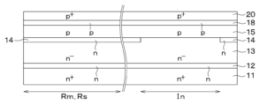
- 3A to 3C are cross-sectional views showing a manufacturing process of the SiC semiconductor device of the first embodiment.
- 6B is a cross-sectional view showing a manufacturing process following FIG. 6A.
- 6C is a cross-sectional view showing a manufacturing process following FIG. 6B.
- 6D is a cross-sectional view showing a manufacturing process following FIG. 6C.
- FIG. 6B is a cross-sectional view showing a manufacturing process following FIG. 6D.
- the SiC semiconductor device of this embodiment has a cell region 1 which is an active region in which an element operates, and an outer peripheral region 2 which surrounds the cell region 1.
- the cell region 1 has a main cell region Rm in which main cells are provided, a sense cell region Rs in which sense cells are provided, and an element isolation region In which is disposed between the main cell region Rm and the sense cell region Rs and electrically isolates the main cell region Rm from the sense cell region Rs.
- the SiC semiconductor device of this embodiment is capable of detecting the main current flowing through the main cell region Rm based on the sense current flowing through the sense cell region Rs and the area ratio.
- various pads 3 are formed for controlling elements provided in the cell region 1 of the SiC semiconductor device, for temperature detection, etc.
- the sense cell region Rs is disposed adjacent to the main cell region Rm.
- the element isolation region In is disposed in a frame shape so as to surround the sense cell region Rs.
- Semiconductor elements having a similar trench gate structure are formed in the main cell region Rm and the sense cell region Rs.
- the outer peripheral region 2 is configured to have a guard ring portion 2a having a peripheral voltage-resistant structure, and a connecting portion 2b arranged inside the guard ring portion 2a.
- the outer peripheral region 2 is configured to have a guard ring portion 2a and a connecting portion 2b arranged between the cell region 1 and the guard ring portion 2a.
- a SiC semiconductor device in which an n-channel vertical MOSFET is provided as a semiconductor element with a trench gate structure in the cell region 1 will be described with reference to Figs. 2 to 5.
- vertical MOSFETs with the same structure are formed in the main cell region Rm and the sense cell region Rs.
- one direction in the surface direction of the semiconductor substrate 10 described later is defined as the X-axis direction
- a direction intersecting with the one direction in the surface direction of the semiconductor substrate 10 is defined as the Y-axis direction
- a direction intersecting with the X-axis direction and the Y-axis direction is defined as the Z-axis direction.
- the X-axis direction, the Y-axis direction, and the Z direction are mutually orthogonal.
- the Z-axis direction in this embodiment corresponds to the thickness direction of the semiconductor substrate 10 described later, and also corresponds to the stacking direction of the substrate 11 and the low concentration layer 13 described later.
- the Y-axis direction is, for example, the ⁇ 11-20> direction.
- the SiC semiconductor device is constructed using a semiconductor substrate 10 on which a vertical MOSFET element is formed.
- the semiconductor substrate 10 is constructed by forming various semiconductor layers made of SiC on an n + type substrate 11 made of SiC.
- the substrate 11 has an off angle of 0 to 8° with respect to the (0001) Si surface, an n-type impurity concentration of nitrogen, phosphorus, etc. of 1.0 ⁇ 10 19 /cm 3 , and a thickness of about 300 ⁇ m.
- the substrate 11 constitutes a drain region.
- an n-type buffer layer 12 made of SiC is formed on the surface of the substrate 11.
- the buffer layer 12 is formed by epitaxial growth on the surface of the substrate 11.
- the buffer layer 12 has an n-type impurity concentration between that of the substrate 11 and the low concentration layer 13 described below, and has a thickness of about 1 ⁇ m.
- n - type low-concentration layer 13 made of SiC is formed on the surface of the buffer layer 12, and has an n-type impurity concentration of, for example, 5.0 ⁇ 10 15 to 2.0 ⁇ 10 16 /cm 3 and a thickness of about 7 to 15 ⁇ m.
- the low-concentration layer 13 may have a constant impurity concentration in the Z-axis direction, but it is preferable that the concentration distribution is inclined so that the low-concentration layer 13 is higher on the substrate 11 side than on the side away from the substrate 11.
- the low-concentration layer 13 corresponds to a first impurity region.
- the JFET layer 14 and the first deep layer 15 are formed in the surface portion of the low concentration layer 13 in the cell region 1.
- the JFET layer 14 and the first deep layer 15 each extend along the X-axis direction and have linear portions arranged alternately and repeatedly in the Y-axis direction.
- the JFET layer 14 and the first deep layer 15 are each formed in stripes extending along the X-axis direction in the normal direction (hereinafter simply referred to as the normal direction) to the surface of the substrate 11, and are arranged alternately along the Y-axis direction.
- the normal direction to the surface of the substrate 11 it can also be said that when viewed from the normal direction to the surface of the substrate 11.
- the normal direction to the surface of the substrate 11 is also the direction along the stacking direction of the drift layer 17 and the base layer 18 described later, and is the direction along the Z-axis direction.
- the JFET layer 14 is of n-type with a higher impurity concentration than the low concentration layer 13, and has a thickness of 0.3 to 1.5 ⁇ m.
- the JFET layer 14 has an n-type impurity concentration of about 5.0 ⁇ 10 16 to 1.0 ⁇ 10 17 /cm 3.
- the first deep layer 15 has a p-type impurity concentration of about 2.0 ⁇ 10 17 to 2.0 ⁇ 10 18 /cm 3.
- the JFET layer 14 is not formed in the element isolation region In of the cell region 1. That is, the JFET layer 14 is formed only in the main cell region Rm and the sense cell region Rs in the cell region 1. In this embodiment, the region in the cell region 1 where the JFET layer 14 is not formed is the element isolation region In.
- the first deep layer 15 may be the same depth as the JFET layer 14, or may be deeper or shallower than the JFET layer 14.
- the first deep layer 15 is formed shallower than the JFET layer 14. That is, the first deep layer 15 is formed so that its bottom is located within the JFET layer 14. In other words, the first deep layer 15 is formed so that the JFET layer 14 is located between the first deep layer 15 and the low concentration layer 13. This suppresses the spread of the depletion layer into the JFET layer 14 between the first deep layers 15, thereby reducing the on-resistance.
- the JFET layer 14 and the first deep layer 15 are formed by appropriately ion-implanting impurities into the surface layer of the low concentration layer 13.
- a JFET layer 14 is extended on the surface of the low concentration layer 13 in the guard ring portion 2a of the peripheral region 2, and multiple p-type guard rings 16 are provided within this JFET layer 14 so as to surround the cell region 1.
- the top surface layout of the guard rings 16 is a square or a circle with rounded corners in the normal direction.
- a p-type connecting layer 15a is provided on the surface portion of the low concentration layer 13 in the connecting portion 2b of the peripheral region 2.
- the connecting layer 15a is disposed so that its inner edge side surrounds the cell region 1, and its outer edge side is disposed up to the boundary position with the guard ring portion 2a.
- the connecting layer 15a is formed by extending the first deep layer 15 up to the connecting portion 2b, and has the same depth and p-type impurity concentration as the first deep layer 15.
- a base layer 18, a source region 19, a contact region 20, etc. are formed on the JFET layer 14 and the first deep layer 15 in the cell region 1.
- the base layer 18 is of p-type and is formed on the JFET layer 14 and the first deep layer 15. Therefore, the first deep layer 15 is connected to the base layer 18.
- the base layer 18 has, for example, a p-type impurity concentration of 5.0 ⁇ 10 16 to 2.0 ⁇ 10 19 /cm 3 and a thickness of about 2.0 ⁇ m.
- the source region 19 is n + type and is formed in the surface layer of the base layer 18.
- the contact region 20 is p + type and is formed in the surface layer of the base layer 18. Specifically, the source region 19 is formed so as to contact the side of a trench 21 described later, and the contact region 20 is formed on the opposite side of the source region 19 to the trench 21 described later.
- the source region 19 has an n-type impurity concentration in the surface layer, i.e., a surface concentration of, for example, 1.0 ⁇ 10 18 /cm 3 , and a thickness of about 0.3 ⁇ m.
- the contact region 20 has a p-type impurity concentration in the surface layer, i.e., a surface concentration of, for example, 1.0 ⁇ 10 21 /cm 3 , and a thickness of about 0.3 ⁇ m.
- the source region 19 corresponds to a second impurity region.
- the base layer 18, contact region 20, and surface portion of the low concentration layer 13 are formed on the low concentration layer 13, JFET layer 14, first deep layer 15, and connecting layer 15a in the connecting portion 2b of the outer peripheral region 2.
- the base layer 18 and contact region 20 are formed on the connecting layer 15a and extend from the cell region 1.
- the base layer 18 and contact region 20 are not formed, and the surface portion of the low concentration layer 13 is formed.
- the base layer 18 and contact region 20 in the outer peripheral region 2 are extended from the cell region 1 and formed halfway in the connecting portion 2b, and are not formed in the connecting portion 2b and guard ring portion 2a outside of that.
- the entire surface layer of the connecting portion 2b is made into a contact region 20, and outside of that, the entire surface layers of the connecting portion 2b and the guard ring portion 2a are made into a low concentration layer 13.
- the semiconductor substrate 10 is configured to include the substrate 11, buffer layer 12, low concentration layer 13, JFET layer 14, first deep layer 15, base layer 18, source region 19, contact region 20, etc. And since each layer that configures the semiconductor substrate 10 is configured from SiC, it can be said that the semiconductor substrate 10 is configured from SiC. Also, in this embodiment, on the inner edge side of the cell region 1 and the connecting portion 2b, one surface 10a of the semiconductor substrate 10 is configured from the source region 19, contact region 20, etc., and the other surface 10b of the semiconductor substrate 10 is configured from the substrate 11.
- the JFET layer 14, the first deep layer 15, the connecting layer 15a, the guard ring 16, the base layer 18, the source region 19, and the contact region 20 are composed of ion-implanted layers formed by ion implantation.
- a trench 21 is formed in the semiconductor substrate 10, penetrating the source region 19, base layer 18, etc., and reaching the JFET layer 14 and first deep layer 15 from the one surface 10a side.
- the trench 21 corresponds to a gate trench, has a depth such that its bottom surface is located within the JFET layer 14 and first deep layer 15, and has a width of, for example, 0.4 to 0.8 ⁇ m.
- the trenches 21 are formed so that multiple ones extend along the Y-axis direction, and are arranged at equal intervals of B1 in the X-axis direction to form a stripe shape, as shown in FIG. 3.
- the trenches 21 are formed so that their longitudinal direction is perpendicular to the longitudinal direction of the first deep layer 15.
- the second deep layer 30 is composed of a p-type layer with a lower impurity concentration than the first deep layer 15.
- the second deep layer 30 is formed along the longitudinal direction of the trench 21.
- the second deep layer 30 extends along the Y-axis direction intersecting with the first deep layer 15.
- the second deep layer 30 in this embodiment is formed so that its bottom surface reaches the low concentration layer 13, penetrating the JFET layer 14 and the first deep layer 15.
- the second deep layer 30 By forming the second deep layer 30 along the bottom surface of the trench 21, it is possible to suppress the penetration of the electric field into the gate insulating film 22 located at the bottom of the trench 21, and to suppress the breakdown of the oxide film. In addition, by forming the second deep layer 30 so as to be in contact with the bottom surface of the trench 21, it is possible to reduce the electrostatic capacitance between the gate electrode 23 and the lower electrode 28, i.e., the feedback capacitance, and to improve the switching speed. Furthermore, since the second deep layer 30 is formed so that the bottom surface thereof penetrates the JFET layer 14 and the first deep layer 15 and reaches the low concentration layer 13, the creeping up of the electric field to the JFET layer 14 disposed between the second deep layers 30 is suppressed, and the breakdown voltage can be improved. In addition, since breakdown is more likely to occur in the second deep layer 30 that protrudes downward when an overvoltage is applied, breakdown is more likely to occur in the cell region 1, and the avalanche resistance can be improved.
- the second deep layer 30 may be divided into multiple parts along the Y-axis direction. However, the second deep layer 30 is formed so as to be electrically connected to the base layer 18 via the first deep layer 15.
- a gate insulating film 22 is formed on the inner wall surface of the trench 21, and a gate electrode 23 made of doped Poly-Si or the like is formed on the gate insulating film 22.
- the gate insulating film 22 is formed by thermally oxidizing the inner wall surface of the trench 21, or by forming an insulating film by a CVD (short for chemical vapor deposition) method.
- the gate insulating film 22 has a thickness of about 100 nm on both the side and bottom sides of the trench 21.
- the gate insulating film 22 is formed on the inner wall surface of the trench 21 as well as on one surface 10a of the semiconductor substrate 10. In the cell region 1, a contact hole 22a is formed in the gate insulating film 22, exposing the source region 19 and the contact region 20.
- An interlayer insulating film 24 is formed on one surface 10a of the semiconductor substrate 10 so as to cover the gate electrode 23, the gate insulating film 22, etc.
- the interlayer insulating film 24 is made of BPSG (short for borophosphosilicate glass) or the like. Note that in FIG. 2, the interlayer insulating film 24 and the like located above the one surface 10a of the semiconductor substrate 10 are omitted.
- the interlayer insulating film 24 has a contact hole 24a formed in the cell region 1, which communicates with the contact hole 22a and exposes the source region 19 and the contact region 20. As shown in FIG. 4, the interlayer insulating film 24 has a contact hole 24b formed therein, which exposes the portion of the gate electrode 23 that extends to the connecting portion 2b.
- an upper electrode 25 is formed, which is electrically connected to the source region 19 and the contact region 20 through the contact holes 22a and 24a.
- the upper electrodes 25 are provided separately for the main cell region Rm and the sense cell region Rs. Each upper electrode 25 can be electrically connected to the outside separately. In this embodiment, the upper electrode 25 corresponds to the first electrode.
- a gate wiring 26 is formed, which is electrically connected to the gate electrode 23 through the contact hole 24b. Although not shown in FIG. 1, the gate wiring 26 is formed along the outer edge of the cell region 1, for example, along the right, left, and lower sides of the SiC semiconductor device that is a rectangular chip shown in FIG. 1.
- the upper electrode 25 in this embodiment is composed of multiple metals, such as Ni/Al.
- the portion of the multiple metals that contacts the n-type SiC, i.e., the portion that constitutes the source region 19, is composed of a metal that can make ohmic contact with the n-type SiC.
- At least the portion of the multiple metals that contacts the p-type SiC, i.e., the contact region 20, is composed of a metal that can make ohmic contact with the p-type SiC.
- the gate wiring 26 may be composed in the same manner as the upper electrode 25, or may be composed of Al-Si, etc.
- a protective film 27 made of polyimide or the like is formed to cover the connecting portion 2b and the guard ring portion 2a.
- the protective film 27 is formed from the outer peripheral region 2 to the outer edge of the cell region 1 in order to suppress the occurrence of creeping discharge between the upper electrode 25 and a lower electrode 28 described below.
- the protective film 27 is formed in the cell region 1 so as to cover the portion of the upper electrode 25 on the outer peripheral region 2 side while exposing the portion of the upper electrode 25 on the inner edge side.
- a lower electrode 28 is formed on the other surface 10b of the semiconductor substrate 10, and is electrically connected to the substrate 11.
- the lower electrode 28 corresponds to the second electrode.
- an n-channel type inversion type trench gate structure MOSFET is formed in the main cell region Rm and the sense cell region Rs due to this structure.
- the element isolation region In is formed to surround the sense cell region Rs and is disposed between the main cell region Rm and the sense cell region Rs.
- the element isolation region In has a structure including a substrate 11, a buffer layer 12, and a low concentration layer 13, similar to the cell region 1.
- the first deep layer 15 is formed in the surface portion of the low concentration layer 13, but the JFET layer 14 is not formed.
- the first deep layer 15 is also arranged with a gap between the main cell region Rm side and the sense cell region Rs side, and is separated between the main cell region Rm and the sense cell region Rs.
- a base layer 18 and a contact region 20 are also formed on the first deep layer 15.
- the base layer 18 is arranged in contact with the first deep layer 15.
- the contact region 20 is also formed in the surface layer of the base layer 18.
- the base layer 18 and the contact region 20 are also arranged with a gap between the main cell region Rm side and the sense cell region Rs side, and are separated between the main cell region Rm and the sense cell region Rs.
- each component in the element isolation region In has the same impurity concentration as that of the cell region 1.
- an isolation trench 40 is formed as an isolation structure so as to reach the first deep layer 15.
- a plurality of isolation trenches 40 two in this embodiment, are provided, each formed to surround the sense cell region Rs.
- Each isolation trench 40 is formed with the same depth and width, and is spaced apart from each other by a distance B2, and is not connected.
- the distance B2 is set to be equal to or less than the distance B1 between adjacent trenches 21 formed in the cell region 1.
- an isolation deep layer 41 is formed at the bottom of this isolation trench 40 so as to contact the bottom surface of the isolation trench 40.
- the isolation deep layer 41 is formed over the entire bottom of the isolation trench 40.
- the isolation deep layer 41 may be separated between the main cell region Rm side and the sense cell region Rs side, and may protrude outward from the bottom surface of the isolation trench 40.
- the isolation trench 40 and isolation deep layer 41 formed in the element isolation region In have the same configuration as the trench 21 and second deep layer 30 formed in the cell region 1. That is, the isolation trench 40 is formed to the same depth and width as the trench 21.
- the isolation deep layer 41 has the same p-type impurity concentration and depth as the second deep layer 30.
- the isolation trench 40 can be formed simultaneously with the trench 21, and the isolation deep layer 41 can be formed simultaneously with the second deep layer 30. If the process for forming the isolation trench 40 and isolation deep layer 41 is shared with the process for forming the trench 21 and second deep layer 30, the manufacturing process can be simplified.
- each isolation trench 40 do not need to be the same, and they do not need to be the same as the width and depth of the trench 21.
- the width of the isolation trench 40 is made larger, for example, larger than the width of two trenches 21 connected together, variations will occur in the workmanship when the trench 21 and the isolation trench 40 are formed.
- the shape and workmanship of the gate insulating film 22 formed on the surface will also vary from that formed on the surface of the trench 21 in the cell region 1, which may affect the yield. For this reason, it is preferable to align the width of each isolation trench 40 to the width of the trench 21.
- each isolation trench 40 is aligned to the width of the trench 21, it is also easier to adjust the withstand voltage and withstand capacity balance between the cell region 1 and the element isolation region In. Note that, although it is preferable that the widths are the same, aligning the widths here means that they are manufactured with the aim of having the same width, and it does not matter if they include manufacturing errors.
- a gate insulating film 22 is formed on the surface of the semiconductor substrate 10 in the element isolation region In, including the inside of the isolation trench 40.
- An isolation gate electrode 42 is formed on the gate insulating film 22.
- the isolation gate electrode 42 is electrically connected to the gate electrode 23, but it may be separated. If the isolation gate electrode 42 is electrically separated from the gate electrode 23, a gate voltage is not applied to the isolation gate electrode 42 during element operation, thereby improving the breakdown voltage.
- An interlayer insulating film 24 and a protective film 27 are formed to cover the isolation gate electrode 42.
- the element isolation region In is configured with this structure.
- the isolation trench 40 and isolation deep layer 41 the base layer 18 and contact region 20 on the main cell region Rm side are electrically isolated from the base layer 18 and contact region 20 on the sense cell region Rs side.
- the isolation deep layer 41 it is possible to suppress the equipotential line from rising between the main cell region Rm and the sense cell region Rs, ensuring a sufficient breakdown voltage.
- n - type, n-type, and n + type correspond to the first conductivity type
- p-type and p + type correspond to the second conductivity type.
- the first deep layer 15 and the JFET layer 14 are provided at a position deeper than the trench 21. Therefore, the depletion layer formed between the first deep layer 15 and the JFET layer 14 suppresses the rise of the equipotential lines due to the influence of the drain voltage, making it difficult for a high electric field to penetrate the gate insulating film 22. Furthermore, since the second deep layer 30, which serves as an electric field relaxation layer, is provided at the bottom of the trench 21, it becomes even more difficult for a high electric field to penetrate the gate insulating film 22. Therefore, in this embodiment, it is possible to suppress the gate insulating film 22 from being destroyed.
- the base layer 18 and contact region 20 on the main cell region Rm side and the sense cell side are electrically isolated by the isolation trench 40, while an isolation deep layer 41 is formed at the bottom of the isolation trench 40. Therefore, the rise of the equipotential line due to the influence of the drain voltage is suppressed even in the element isolation region In.
- the element isolation region In can have a higher breakdown voltage than the cell region 1. This makes it possible to prevent the element isolation region In, which tends to have a small area, from breaking down first. Therefore, the breakdown voltage of the SiC semiconductor device is determined by the breakdown voltage of the cell region 1, and the breakdown voltage of the SiC semiconductor device can be designed based on the breakdown voltage design of the cell region 1.
- the inventors investigated the drain-source breakdown voltage. Specifically, at a temperature of 25°C, the source voltages of both the main cell region Rm and the sense cell region Rs were set to 0V, the gate voltage was set to -3.5V, and the breakdown voltage was examined based on SIM analysis while changing the spacing B2. As a result, when the spacing B2 was equal to or smaller than the spacing B1 of the trench 21 in the cell region 1, a high breakdown voltage of 1400V or more could be obtained in all cases. Furthermore, when a similar analysis was performed at a temperature of 175°C, a high breakdown voltage of 1400V or more could be obtained.
- the source leakage between the main cell region Rm and the sense cell region Rs was examined by SIM analysis, and it was found that source leakage due to short circuiting could be suppressed because the isolation deep layer 41 was separated between the main cell region Rm side and the sense cell region Rs side.
- the width of the element isolation region In is not important as long as it can ensure the breakdown voltage and suppress source leakage.
- the element isolation region In is an ineffective region through which current does not easily flow. Therefore, it is preferable to make the width of the element isolation region In as narrow as possible while taking into consideration the breakdown voltage and source leakage. Based on this, the spacing B1, width, and number of isolation trenches 40 can be set.
- a substrate 11 is prepared, and then a buffer layer 12 and a low-concentration layer 13 are epitaxially grown on one side of the substrate 11. Then, a mask (not shown) with an opening corresponding to the JFET layer 14 is placed on the surface of the low-concentration layer 13, and n-type impurities are ion-implanted to form the JFET layer 14.
- a mask (not shown) with an opening corresponding to the first deep layer 15 is formed again, and p-type impurities are ion-implanted to form the first deep layer 15 as shown in FIG. 6B.
- a mask (not shown) with an opening corresponding to the base layer 18 is also formed, and p-type impurities are ion-implanted to form the base layer 18.
- p-type impurities are further ion-implanted using a mask with an opening corresponding to the contact region 20 to form the contact region 20 on the base layer 18.
- a mask (not shown) with an opening corresponding to the source region 19 is formed, and n-type impurities are ion-implanted to form the source region 19 as shown in FIG. 6C.
- the contact region 20 is formed up to the part that will become the source region 19, but by increasing the dose of the n-type impurity, it is possible to drive it back to n-type and form the source region 19.
- a mask 50 is placed with openings corresponding to the trench 21 and the isolation trench 40, and then the trench 21 and the isolation trench 40 are simultaneously formed by dry etching.
- the same mask 50 is used to ion-implant p-type impurities to form the second deep layer 30 at the bottom of the trench 21 and at the same time form the isolation deep layer 41 at the bottom of the isolation trench 40.
- the gate insulating film 22 is formed by thermal oxidation or CVD, and then the gate electrode 23 and the isolated gate electrode 42 are simultaneously formed by deposition and patterning of doped polysilicon. Then, the process of forming the interlayer insulating film 24, the process of forming the upper electrode 25 and gate wiring 26, the process of forming the protective film 27, and the process of forming the lower electrode 28 on the back side of the substrate 11 are carried out using the conventional processes. This completes the SiC semiconductor device according to this embodiment.
- an isolation trench 40 is formed in the element isolation region In to isolate the base layer 18 and contact region 20 on the main cell region Rm side and the sense cell region Rs side. This allows accurate electrical isolation between the base layer 18 and contact region 20 on the main cell region Rm side and the base layer 18 and contact region 20 on the sense cell region Rs side.
- isolation deep layer 41 it is possible to suppress the rise of the equipotential line between the main cell region Rm and the sense cell region Rs, and to ensure the breakdown voltage. Furthermore, since multiple isolation trenches 40 are formed, it is not necessary to widen the width of each isolation trench 40, as is the case when isolation deep layers 41 are formed at both ends of a single wide isolation trench 40, and therefore adjacent isolation deep layers 41 can be prevented from being connected.
- the isolation deep layer 41 when the trench 21 and the isolation trench 40 formed in the cell region are formed simultaneously, if the widths are different, there will be variations in the finish, and when the isolation deep layer 41 is formed at both ends of a single wide isolation trench 40, the trench shape will not be stable.
- the ion implantation mask used when forming the second deep layer 30 and the isolation deep layer 41 will be placed on one surface 10a of the semiconductor substrate 10, but within the isolation trench 40, the mask for isolating the isolation deep layer 41 is placed from the bottom surface of the isolation trench 40. Therefore, the mask height will be different within the isolation trench 40, and there will be variations in the finish of the isolation deep layer 41. Therefore, when the isolation deep layer 41 is formed at both ends of a single wide isolation trench 40, the isolation deep layer 41 will be connected, making it impossible to isolate the main cell region Rm and the sense cell region Rs.
- each isolation trench 40 is spaced apart on the main cell region Rm side and the sense cell region Rs side by a distance B2, each isolation deep layer 41 located at the bottom is also spaced apart from each other. This makes it possible to suppress source leakage due to a short circuit between the main cell region Rm side and the sense cell region Rs side.
- the manufacturing method for a SiC semiconductor device according to this embodiment can also provide the following effects.
- the isolation structure is formed by an isolation trench 40. Therefore, the process of forming the trench 21 and the process of forming the isolation trench 40 can be common, simplifying the manufacturing process and reducing the element manufacturing costs. Furthermore, in the element isolation region In, the isolation trench 40 is formed so as to penetrate the base layer 18 and contact region 20 on the main cell region Rm side and the base layer 18 and contact region 20 on the sense cell region Rs side. Therefore, it is not necessary to pattern the base layer 18 and contact region 20 in detail. In this respect as well, the manufacturing process can be simplified.
- the isolation deep layer 41 is formed by ion-implanting p-type impurities into the bottom of the isolation trench 40 using the mask used when forming the isolation trench 40, so that the isolation deep layer 41 can be formed without any mask misalignment. This allows the isolation trench 40 and the isolation deep layer 41 to be formed without any misalignment, eliminating variations in the finished product and improving yields. Furthermore, the process for forming the isolation deep layer 41 can be shared with the process for forming the second deep layer 30, simplifying the manufacturing process and reducing the cost of manufacturing the elements.
- the first deep layer 15 is formed up to the boundary between the main cell region Rm and the sense cell region Rs, and is in contact with the isolation deep layer 41 formed in the element isolation region In.
- the first deep layer 15 may extend to the bottom of the isolation trench 40 and partially overlap with the isolation deep layer 41, or the first deep layer 15 may be separated from the isolation deep layer 41.
- the first deep layer 15 and the isolation deep layer 41 are too far apart, there is a concern that the withstand voltage will decrease due to the equipotential lines rising up, so it is preferable to make the distance equal to or less than the distance B1 between the trenches 21 in the main cell region Rm.
- two isolation trenches 40 are formed as an example, but three or more may be formed. However, the more isolation trenches 40 are formed, the larger the area of the element isolation region In becomes, which leads to an increase in the chip area, so two trenches are better in terms of area efficiency.
- the bottom surface of the second deep layer 30 may be shallow and located within the JFET layer 14 and the first deep layer 15.
- the second deep layer 30 may be formed so as not to reach the low concentration layer 13. This makes it difficult for the depletion layer to extend from the second deep layer 30, thereby reducing the on-resistance.
- the bottom surface of the isolation deep layer 41 is also formed shallow, but the positions of the bottom surfaces of the second deep layer 30 and the isolation deep layer 41 can be adjusted based on the breakdown voltage design.
- the JFET layer 14, the first deep layer 15, the base layer 18, the contact region 20, and the source region 19 are formed by ion implantation. Some or all of these may be composed of epitaxial layers formed by epitaxial growth.
- the source region 19 may be formed in the surface layer of the base layer 18, or the contact region 20 and source region 19 may not be formed, and the gate insulating film 22 may be formed on the surface of the base layer 18.
- the base layer 18 is formed on the surface of the JFET layer 14 and the first deep layer 15, but an n-type current spreading layer having a higher n-type impurity concentration than the low concentration layer 13 may be formed between them.
- a p-type connection layer may be formed on both sides of the trench 21, and the base layer 18 may be formed on these current spreading layers and connection layers.
- the first deep layer 15 and the base layer 18 are connected through the connection layer.
- the low concentration layer 13, the JFET layer 14, and the current spreading layer are connected, and the drift layer 17 is formed by these.
- the second deep layer 30 and the separation deep layer 41 may be formed deeper than the first deep layer 15, or may be formed to a depth within the thickness of the first deep layer 15.
- the JFET layer 14 is formed in the outer periphery region 2, but the JFET layer 14 may not be formed and only the low concentration layer 13 may be formed.
- the depth of the isolation trench 40 may be different from that of the trench 21.
- the isolation trench 40 may be formed in a process separate from the process of forming the trench 21.
- the isolation deep layer 41 may also be formed in a process separate from the process of forming the second deep layer 30.
- a vertical MOSFET with an n-channel type trench gate structure in which the first conductivity type is n-type and the second conductivity type is p-type is given as an example of the semiconductor element provided in the cell region 1.
- this is merely one example, and it may be a vertical MOSFET with a p-channel type trench gate structure in which the conductivity types of each component are inverted from the n-channel type.
- a vertical IGBT with a similar structure may be used instead of a vertical MOSFET. In the case of an IGBT, it is the same as the vertical MOSFET described in the above embodiment, except that the conductivity type of the substrate 11 in each of the above embodiments is changed from n-type to p-type.
- a bar (-) When indicating a crystal orientation, a bar (-) should normally be placed above the desired number. However, due to limitations on expression based on electronic filing, a bar is placed before the desired number in this specification.
Landscapes
- Element Separation (AREA)
- Junction Field-Effect Transistors (AREA)
- Bipolar Transistors (AREA)
Priority Applications (2)
| Application Number | Priority Date | Filing Date | Title |
|---|---|---|---|
| CN202480027722.8A CN121014274A (zh) | 2023-04-26 | 2024-04-25 | 碳化硅半导体装置 |
| US19/365,584 US20260047154A1 (en) | 2023-04-26 | 2025-10-22 | Silicon carbide semiconductor device |
Applications Claiming Priority (2)
| Application Number | Priority Date | Filing Date | Title |
|---|---|---|---|
| JP2023072620A JP2024157940A (ja) | 2023-04-26 | 2023-04-26 | 炭化珪素半導体装置 |
| JP2023-072620 | 2023-04-26 |
Related Child Applications (1)
| Application Number | Title | Priority Date | Filing Date |
|---|---|---|---|
| US19/365,584 Continuation US20260047154A1 (en) | 2023-04-26 | 2025-10-22 | Silicon carbide semiconductor device |
Publications (1)
| Publication Number | Publication Date |
|---|---|
| WO2024225406A1 true WO2024225406A1 (ja) | 2024-10-31 |
Family
ID=93256607
Family Applications (1)
| Application Number | Title | Priority Date | Filing Date |
|---|---|---|---|
| PCT/JP2024/016351 Ceased WO2024225406A1 (ja) | 2023-04-26 | 2024-04-25 | 炭化珪素半導体装置 |
Country Status (4)
| Country | Link |
|---|---|
| US (1) | US20260047154A1 (https=) |
| JP (1) | JP2024157940A (https=) |
| CN (1) | CN121014274A (https=) |
| WO (1) | WO2024225406A1 (https=) |
Citations (5)
| Publication number | Priority date | Publication date | Assignee | Title |
|---|---|---|---|---|
| US20080290461A1 (en) * | 2007-05-25 | 2008-11-27 | Ami Semiconductor Belgium Bvba | Deep trench isolation for power semiconductors |
| US20140217495A1 (en) * | 2013-02-04 | 2014-08-07 | Infineon Technologies Austria Ag | Integrated Circuit with Power and Sense Transistors |
| JP2016063107A (ja) * | 2014-09-19 | 2016-04-25 | トヨタ自動車株式会社 | 半導体装置 |
| JP2021048276A (ja) * | 2019-09-19 | 2021-03-25 | 三菱電機株式会社 | 半導体装置 |
| JP2021093481A (ja) * | 2019-12-12 | 2021-06-17 | 株式会社デンソー | 炭化珪素半導体装置 |
-
2023
- 2023-04-26 JP JP2023072620A patent/JP2024157940A/ja active Pending
-
2024
- 2024-04-25 CN CN202480027722.8A patent/CN121014274A/zh active Pending
- 2024-04-25 WO PCT/JP2024/016351 patent/WO2024225406A1/ja not_active Ceased
-
2025
- 2025-10-22 US US19/365,584 patent/US20260047154A1/en active Pending
Patent Citations (5)
| Publication number | Priority date | Publication date | Assignee | Title |
|---|---|---|---|---|
| US20080290461A1 (en) * | 2007-05-25 | 2008-11-27 | Ami Semiconductor Belgium Bvba | Deep trench isolation for power semiconductors |
| US20140217495A1 (en) * | 2013-02-04 | 2014-08-07 | Infineon Technologies Austria Ag | Integrated Circuit with Power and Sense Transistors |
| JP2016063107A (ja) * | 2014-09-19 | 2016-04-25 | トヨタ自動車株式会社 | 半導体装置 |
| JP2021048276A (ja) * | 2019-09-19 | 2021-03-25 | 三菱電機株式会社 | 半導体装置 |
| JP2021093481A (ja) * | 2019-12-12 | 2021-06-17 | 株式会社デンソー | 炭化珪素半導体装置 |
Also Published As
| Publication number | Publication date |
|---|---|
| CN121014274A (zh) | 2025-11-25 |
| US20260047154A1 (en) | 2026-02-12 |
| JP2024157940A (ja) | 2024-11-08 |
Similar Documents
| Publication | Publication Date | Title |
|---|---|---|
| US11469318B2 (en) | Superjunction semiconductor device having parallel PN structure with column structure and method of manufacturing the same | |
| US12027578B2 (en) | Semiconductor device | |
| US8957502B2 (en) | Semiconductor device | |
| US7808003B2 (en) | Silicon carbide semiconductor device | |
| US6825565B2 (en) | Semiconductor device | |
| JP5509908B2 (ja) | 半導体装置およびその製造方法 | |
| CN112563319B (zh) | 半导体装置 | |
| JP7593225B2 (ja) | 炭化珪素半導体装置 | |
| JPWO2017010393A1 (ja) | 半導体装置および半導体装置の製造方法 | |
| CN107731911A (zh) | 半导体装置 | |
| US11538935B2 (en) | Silicon carbide semiconductor device | |
| CN111816694B (zh) | 超结半导体装置及超结半导体装置的制造方法 | |
| KR102400895B1 (ko) | 반도체 장치 및 그 제조 방법 | |
| US10707301B2 (en) | Semiconductor device and method of manufacturing semiconductor device | |
| JP2025100911A (ja) | 炭化珪素半導体装置 | |
| WO2024225406A1 (ja) | 炭化珪素半導体装置 | |
| JP5023423B2 (ja) | 縦型絶縁ゲート型電界効果トランジスタおよびその製造方法 | |
| JP2023173412A (ja) | 炭化珪素半導体装置 | |
| JP2024073983A (ja) | 炭化珪素半導体装置 | |
| CN114388612A (zh) | 半导体装置及半导体装置的制造方法 | |
| US20260047129A1 (en) | Silicon carbide semiconductor device | |
| US20250374616A1 (en) | Semiconductor device | |
| US12622026B2 (en) | Semiconductor device and method for manufacturing the same | |
| JP2026042671A (ja) | 超接合半導体装置 | |
| JP2003318393A (ja) | 絶縁ゲート型半導体装置およびその製造方法 |
Legal Events
| Date | Code | Title | Description |
|---|---|---|---|
| 121 | Ep: the epo has been informed by wipo that ep was designated in this application |
Ref document number: 24797151 Country of ref document: EP Kind code of ref document: A1 |
|
| NENP | Non-entry into the national phase |
Ref country code: DE |
|
| 122 | Ep: pct application non-entry in european phase |
Ref document number: 24797151 Country of ref document: EP Kind code of ref document: A1 |