WO2024225385A1 - 表示装置用積層体および表示装置 - Google Patents
表示装置用積層体および表示装置 Download PDFInfo
- Publication number
- WO2024225385A1 WO2024225385A1 PCT/JP2024/016274 JP2024016274W WO2024225385A1 WO 2024225385 A1 WO2024225385 A1 WO 2024225385A1 JP 2024016274 W JP2024016274 W JP 2024016274W WO 2024225385 A1 WO2024225385 A1 WO 2024225385A1
- Authority
- WO
- WIPO (PCT)
- Prior art keywords
- laminate
- display device
- laminate film
- layer
- thickness
- Prior art date
- Legal status (The legal status is an assumption and is not a legal conclusion. Google has not performed a legal analysis and makes no representation as to the accuracy of the status listed.)
- Ceased
Links
Images



Classifications
-
- B—PERFORMING OPERATIONS; TRANSPORTING
- B32—LAYERED PRODUCTS
- B32B—LAYERED PRODUCTS, i.e. PRODUCTS BUILT-UP OF STRATA OF FLAT OR NON-FLAT, e.g. CELLULAR OR HONEYCOMB, FORM
- B32B23/00—Layered products comprising a layer of cellulosic plastic substances, i.e. substances obtained by chemical modification of cellulose, e.g. cellulose ethers, cellulose esters, viscose
- B32B23/04—Layered products comprising a layer of cellulosic plastic substances, i.e. substances obtained by chemical modification of cellulose, e.g. cellulose ethers, cellulose esters, viscose comprising such cellulosic plastic substance as the main or only constituent of a layer, which is next to another layer of the same or of a different material
- B32B23/08—Layered products comprising a layer of cellulosic plastic substances, i.e. substances obtained by chemical modification of cellulose, e.g. cellulose ethers, cellulose esters, viscose comprising such cellulosic plastic substance as the main or only constituent of a layer, which is next to another layer of the same or of a different material of synthetic resin
-
- B—PERFORMING OPERATIONS; TRANSPORTING
- B32—LAYERED PRODUCTS
- B32B—LAYERED PRODUCTS, i.e. PRODUCTS BUILT-UP OF STRATA OF FLAT OR NON-FLAT, e.g. CELLULAR OR HONEYCOMB, FORM
- B32B27/00—Layered products comprising a layer of synthetic resin
- B32B27/06—Layered products comprising a layer of synthetic resin as the main or only constituent of a layer, which is next to another layer of the same or of a different material
- B32B27/08—Layered products comprising a layer of synthetic resin as the main or only constituent of a layer, which is next to another layer of the same or of a different material of synthetic resin
-
- B—PERFORMING OPERATIONS; TRANSPORTING
- B32—LAYERED PRODUCTS
- B32B—LAYERED PRODUCTS, i.e. PRODUCTS BUILT-UP OF STRATA OF FLAT OR NON-FLAT, e.g. CELLULAR OR HONEYCOMB, FORM
- B32B27/00—Layered products comprising a layer of synthetic resin
- B32B27/28—Layered products comprising a layer of synthetic resin comprising synthetic resins not wholly covered by any one of the sub-groups B32B27/30 - B32B27/42
- B32B27/281—Layered products comprising a layer of synthetic resin comprising synthetic resins not wholly covered by any one of the sub-groups B32B27/30 - B32B27/42 comprising polyimides
-
- B—PERFORMING OPERATIONS; TRANSPORTING
- B32—LAYERED PRODUCTS
- B32B—LAYERED PRODUCTS, i.e. PRODUCTS BUILT-UP OF STRATA OF FLAT OR NON-FLAT, e.g. CELLULAR OR HONEYCOMB, FORM
- B32B27/00—Layered products comprising a layer of synthetic resin
- B32B27/30—Layered products comprising a layer of synthetic resin comprising vinyl (co)polymers; comprising acrylic (co)polymers
- B32B27/308—Layered products comprising a layer of synthetic resin comprising vinyl (co)polymers; comprising acrylic (co)polymers comprising acrylic (co)polymers
-
- B—PERFORMING OPERATIONS; TRANSPORTING
- B32—LAYERED PRODUCTS
- B32B—LAYERED PRODUCTS, i.e. PRODUCTS BUILT-UP OF STRATA OF FLAT OR NON-FLAT, e.g. CELLULAR OR HONEYCOMB, FORM
- B32B27/00—Layered products comprising a layer of synthetic resin
- B32B27/34—Layered products comprising a layer of synthetic resin comprising polyamides
-
- B—PERFORMING OPERATIONS; TRANSPORTING
- B32—LAYERED PRODUCTS
- B32B—LAYERED PRODUCTS, i.e. PRODUCTS BUILT-UP OF STRATA OF FLAT OR NON-FLAT, e.g. CELLULAR OR HONEYCOMB, FORM
- B32B27/00—Layered products comprising a layer of synthetic resin
- B32B27/36—Layered products comprising a layer of synthetic resin comprising polyesters
-
- B—PERFORMING OPERATIONS; TRANSPORTING
- B32—LAYERED PRODUCTS
- B32B—LAYERED PRODUCTS, i.e. PRODUCTS BUILT-UP OF STRATA OF FLAT OR NON-FLAT, e.g. CELLULAR OR HONEYCOMB, FORM
- B32B7/00—Layered products characterised by the relation between layers; Layered products characterised by the relative orientation of features between layers, or by the relative values of a measurable parameter between layers, i.e. products comprising layers having different physical, chemical or physicochemical properties; Layered products characterised by the interconnection of layers
- B32B7/02—Physical, chemical or physicochemical properties
- B32B7/022—Mechanical properties
-
- B—PERFORMING OPERATIONS; TRANSPORTING
- B32—LAYERED PRODUCTS
- B32B—LAYERED PRODUCTS, i.e. PRODUCTS BUILT-UP OF STRATA OF FLAT OR NON-FLAT, e.g. CELLULAR OR HONEYCOMB, FORM
- B32B7/00—Layered products characterised by the relation between layers; Layered products characterised by the relative orientation of features between layers, or by the relative values of a measurable parameter between layers, i.e. products comprising layers having different physical, chemical or physicochemical properties; Layered products characterised by the interconnection of layers
- B32B7/04—Interconnection of layers
- B32B7/06—Interconnection of layers permitting easy separation
-
- C—CHEMISTRY; METALLURGY
- C09—DYES; PAINTS; POLISHES; NATURAL RESINS; ADHESIVES; COMPOSITIONS NOT OTHERWISE PROVIDED FOR; APPLICATIONS OF MATERIALS NOT OTHERWISE PROVIDED FOR
- C09J—ADHESIVES; NON-MECHANICAL ASPECTS OF ADHESIVE PROCESSES IN GENERAL; ADHESIVE PROCESSES NOT PROVIDED FOR ELSEWHERE; USE OF MATERIALS AS ADHESIVES
- C09J7/00—Adhesives in the form of films or foils
- C09J7/20—Adhesives in the form of films or foils characterised by their carriers
- C09J7/29—Laminated material
-
- C—CHEMISTRY; METALLURGY
- C09—DYES; PAINTS; POLISHES; NATURAL RESINS; ADHESIVES; COMPOSITIONS NOT OTHERWISE PROVIDED FOR; APPLICATIONS OF MATERIALS NOT OTHERWISE PROVIDED FOR
- C09J—ADHESIVES; NON-MECHANICAL ASPECTS OF ADHESIVE PROCESSES IN GENERAL; ADHESIVE PROCESSES NOT PROVIDED FOR ELSEWHERE; USE OF MATERIALS AS ADHESIVES
- C09J7/00—Adhesives in the form of films or foils
- C09J7/30—Adhesives in the form of films or foils characterised by the adhesive composition
- C09J7/38—Pressure-sensitive adhesives [PSA]
-
- G—PHYSICS
- G02—OPTICS
- G02B—OPTICAL ELEMENTS, SYSTEMS OR APPARATUS
- G02B1/00—Optical elements characterised by the material of which they are made; Optical coatings for optical elements
- G02B1/10—Optical coatings produced by application to, or surface treatment of, optical elements
-
- G—PHYSICS
- G09—EDUCATION; CRYPTOGRAPHY; DISPLAY; ADVERTISING; SEALS
- G09F—DISPLAYING; ADVERTISING; SIGNS; LABELS OR NAME-PLATES; SEALS
- G09F9/00—Indicating arrangements for variable information in which the information is built-up on a support by selection or combination of individual elements
- G09F9/30—Indicating arrangements for variable information in which the information is built-up on a support by selection or combination of individual elements in which the desired character or characters are formed by combining individual elements
- G09F9/301—Indicating arrangements for variable information in which the information is built-up on a support by selection or combination of individual elements in which the desired character or characters are formed by combining individual elements flexible foldable or roll-able electronic displays, e.g. thin LCD, OLED
-
- B—PERFORMING OPERATIONS; TRANSPORTING
- B32—LAYERED PRODUCTS
- B32B—LAYERED PRODUCTS, i.e. PRODUCTS BUILT-UP OF STRATA OF FLAT OR NON-FLAT, e.g. CELLULAR OR HONEYCOMB, FORM
- B32B2457/00—Electrical equipment
- B32B2457/20—Displays, e.g. liquid crystal displays, plasma displays
Definitions
- This disclosure relates to a laminate for a display device and a display device.
- a laminate having functional layers with various properties is arranged on the surface of the display device.
- Laminates placed on the surface of flexible displays are required to be scratch-resistant. For this reason, laminates with high surface hardness are used. Flexible displays are also required to be able to withstand repeated bending without causing display defects, and laminates placed on the surface of flexible displays are required to have bending resistance that prevents peeling or cracking when repeatedly bent. However, increasing the surface hardness of the laminate can result in a decrease in bending resistance. For this reason, it is difficult to achieve both high hardness and bending resistance.
- a replaceable laminate needs to be able to be attached and removed. However, because a replaceable laminate can be removed, it may lift or peel off when repeatedly bent. For this reason, it is difficult to achieve both replaceability and bending resistance at the same time.
- the present disclosure has been made in consideration of the above-mentioned circumstances, and has as its main object to provide a replaceable laminate for a display device that has excellent hardness and flex resistance, and a display device including the same.
- One embodiment of the present disclosure provides a laminate for a display device, comprising: a first laminate film having a first resin substrate and a first functional layer; a bonding layer disposed on a surface of the first laminate film facing the first resin substrate; and a second laminate film disposed on a surface of the bonding layer opposite the first laminate film, the second laminate film having, in this order from the bonding layer side, a second functional layer and a second resin substrate, wherein the first laminate film and the bonding layer are peelable from the second laminate film, the first functional layer has a thickness of 8 ⁇ m or more, an A1 value calculated by the following formula (1) is 0.10 ⁇ 10 ⁇ 3 Pa ⁇ m 3 or more and 0.52 ⁇ 10 ⁇ 3 Pa ⁇ m 3 or less, and an A2 value calculated by the following formula (2) is 0.07 ⁇ 10 ⁇ 3 Pa ⁇ m 3 or less.
- A1 E1 ⁇ h1 3/12 (1)
- A2 E2 ⁇ h2 3/12 (2)
- E1 represents the tensile modulus (Pa) of the first laminate film
- h1 represents the thickness (m) of the first laminate film
- E2 represents the tensile modulus (Pa) of the second laminate film
- h2 represents the thickness (m) of the second laminate film.
- Another embodiment of the present disclosure provides a display device comprising a display panel and the above-described laminate for a display device arranged on the viewer side of the display panel, the laminate for a display device being arranged such that the surface on the second laminate film side faces the display panel.
- the present disclosure has the effect of providing a replaceable laminate for a display device that has excellent hardness and bending resistance.
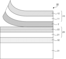
- 1 is a schematic cross-sectional view illustrating a laminate for a display device according to the present disclosure.
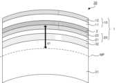
- 1 is a schematic cross-sectional view illustrating a display device according to the present disclosure.
- 1 is a schematic cross-sectional view illustrating a display device according to the present disclosure.
- 1 is a schematic cross-sectional view illustrating a display device according to the present disclosure.
- FIG. 2 is a schematic diagram illustrating a dynamic bending test.
- 1 is a schematic cross-sectional view illustrating a display device according to the present disclosure.
- the term “above” or “below” includes both cases in which another component is placed directly above or below a certain component so as to be in contact with the component, and cases in which another component is placed above or below a certain component with another component in between, unless otherwise specified.
- the term “on the surface side” or “on the surface” includes both cases in which another component is placed directly above or below a certain component so as to be in contact with the component, and cases in which another component is placed above or below a certain component with another component in between, unless otherwise specified.
- the laminate for a display device and the display device in this disclosure are described in detail below.
- the laminate for display device in the present disclosure has a first laminate film having a first resin substrate and a first functional layer, a bonding layer arranged on the surface of the first laminate film on the side of the first resin substrate, and a second laminate film arranged on the surface of the bonding layer opposite to the first laminate film and having, in order from the bonding layer side, a second functional layer and a second resin substrate, the first laminate film and the bonding layer are peelable from the second laminate film, the first resin substrate contains a polyimide resin, the first functional layer has a thickness of 8 ⁇ m or more, the A1 value calculated by the following formula (1) is 0.10 ⁇ 10 -3 Pa ⁇ m 3 or more and 0.52 ⁇ 10 -3 Pa ⁇ m 3 or less, and the A2 value calculated by the following formula (2) is 0.07 ⁇ 10 -3 Pa ⁇ m 3 or less.
- A1 E1 ⁇ h1 3/12 (1)
- A2 E2 ⁇ h2 3/12 (2)
- E1 represents the tensile modulus (Pa) of the first laminate film
- h1 represents the thickness (m) of the first laminate film
- E2 represents the tensile modulus (Pa) of the second laminate film
- h2 represents the thickness (m) of the second laminate film.
- the laminate for a display device 1 has a first laminate film 10 having a first resin substrate 11 and a first functional layer 12, a bonding layer 2 arranged on the surface of the first laminate film 10 facing the first resin substrate 11, and a second laminate film 20 arranged on the surface of the bonding layer 2 facing away from the first laminate film 10 and having, in order from the bonding layer 2 side, a second functional layer 22 and a second resin substrate 21.
- the first resin substrate 11 contains a polyimide resin, and the thickness of the first functional layer 12 is equal to or greater than a predetermined value.
- the A1 value calculated by the above formula (1) is within a predetermined range.
- the A2 value calculated by the above formula (2) is within a predetermined range.
- FIG. 2 is a schematic cross-sectional view showing an example of a display device including a laminate for a display device according to the present disclosure.
- the display device 30 includes a display panel 31 and a laminate for a display device 1 arranged on the viewer's side of the display panel 31.
- the laminate for a display device 1 is arranged so that the surface on the second laminate film 20 side faces the display panel 31.
- An adhesive layer 32 is arranged between the display panel 31 and the laminate for a display device 1.
- the first laminate film 10 and the bonding layer 2 are peelable from the second laminate film 20.
- the first laminate film and the bonding layer can be peeled off from the second laminate film. Therefore, in a display device including a laminate for a display device, if a dent or scratch occurs on the surface of the first functional layer side of the first laminate film, the first laminate film and the bonding layer can be replaced.
- the bonding layer may become lifted or peeled off when the laminate for a display device is repeatedly bent, which means that the bending resistance may decrease.
- a bending moment is applied to a display device 30 including a laminate 10 for a display device from the laminate 10 side of the display device 30, the side of the display device 30 opposite the laminate 10 side for a display device shrinks and the laminate 10 side for a display device of the display device 30 stretches, but there is a surface between them that does not stretch or shrink, i.e., a neutral surface NP.
- a bending moment is applied to a display device 30 including a laminate 10 for a display device from the side opposite the laminate 10 for a display device of the display device 30, the laminate 10 for a display device side of the display device 30 shrinks and the side opposite the laminate 10 for a display device side of the display device 30 stretches, but there is a surface between them that does not stretch or shrink, i.e., a neutral surface NP.
- the strain increases in proportion to the distance from the neutral plane.
- the A2 value is the product of the tensile modulus E2 of the second laminate film and the cube of the thickness of the second laminate film divided by 12 (h2 3 /12).
- the A2 value is equal to or less than a predetermined value, it can be said that the thickness of the second laminate film is relatively thin.
- the distance d1 from the neutral plane NP to the interface between the second laminate film 20 and the bonding layer 2 as shown in FIG. 3 and FIG. 4 is shorter than when the thickness of the second laminate film is thick.
- the strain at the interface between the second laminate film 20 and the bonding layer 2 can be reduced. This can suppress peeling between the bonding layer and the second laminate film. Therefore, although the first laminate film and the bonding layer can be peeled off from the second laminate film, the lifting and peeling of the bonding layer during bending can be suppressed. In particular, even when the display device laminate is repeatedly bent, the lifting and peeling of the bonding layer can be suppressed. Therefore, by having the A2 value be equal to or less than a predetermined value, the bending resistance can be improved.
- the A1 value is the product of the tensile modulus E1 of the first laminate film and the cube of the thickness of the first laminate film divided by 12 (h1 3 /12), and indicates the difficulty of bending the first laminate film. It can be said that the larger the A1 value, the more difficult it is to bend the first laminate film, and the smaller the A1 value, the easier it is to bend the first laminate film.
- the A1 value also serves as an index of the hardness of the first laminate film. The larger the A1 value, the higher the hardness of the first laminate film, and the smaller the A1 value, the lower the hardness of the first laminate film.
- the value obtained by dividing the cube of the thickness of the first laminate film by 12 is adopted with reference to the definition of the second moment of area.
- the A2 value is the product of the tensile modulus E2 of the second laminate film and the cube of the thickness of the second laminate film divided by 12 (h2 3 /12), and indicates the difficulty of bending the second laminate film. It can be said that the larger the A2 value, the more difficult it is to bend the second laminate film, and the smaller the A2 value, the easier it is to bend the second laminate film.
- the A2 value also serves as an index of the hardness of the second laminate film. The larger the A2 value, the higher the hardness of the second laminate film, and the smaller the A2 value, the lower the hardness of the second laminate film.
- the value obtained by dividing the cube of the thickness of the second laminate film by 12 is adopted with reference to the definition of the second moment of area.
- the second moment of area I varies depending on the area of the film. For example, if the area of the film is large, the second moment of area becomes large, and a large force is required to bend the film. On the other hand, if the area of the film is small, the second moment of area becomes small, and the force required to bend the film becomes small.
- the above formula (1) that does not include the thickness of the first laminate film and the above formula (2) that does not include the thickness of the second laminate film are adopted so that the value indicating the difficulty of bending does not change depending on the area of the first laminate film and the area of the second laminate film.
- the first laminate film when the A1 value is equal to or greater than a predetermined value, the first laminate film is less likely to bend and has high hardness. Furthermore, when the A1 value is within a predetermined range, the surface hardness of the first laminate film can be increased by having the thickness of the first functional layer be equal to or greater than a predetermined value. Therefore, deformation of the first laminate film can be suppressed. Furthermore, when the first resin base material contains a polyimide resin, the first resin base material can be made to be more likely to elastically deform and less likely to plastically deform. Therefore, even if the first laminate film is deformed, it is more likely to return to its original shape. Therefore, in a display device including a laminate for a display device, when the surface of the laminate for a display device is pressed, deformation of the first laminate film can be suppressed and the deformation of the first laminate film can be easily restored.
- the second laminate film is easy to bend and has low hardness. Therefore, in a display device including a laminate for a display device, if the bonding layer is deformed when the surface of the laminate for a display device is pressed, the second laminate film is also likely to deform in conjunction with the deformation of the bonding layer. This allows the deformation of the bonding layer to be absorbed by the second laminate film.
- the A1 value is equal to or greater than a predetermined value, and the A1 value is within a predetermined range, the thickness of the first functional layer is equal to or greater than a predetermined value, the first resin substrate contains a polyimide resin, and the A2 value is equal to or less than a predetermined value, the hardness can be increased. Thus, scratch resistance can be improved.
- the first laminate film and the second laminate film are laminated via a bonding layer.
- the inventors of the present disclosure have found that in such a display device laminate, even if the first laminate film alone has a high surface hardness, the entire display device laminate may have a low surface hardness.
- a non-curing adhesive layer such as a pressure-sensitive adhesive layer or a heat-sensitive adhesive layer is usually used for the bonding layer, rather than a curing adhesive layer.
- a non-curing adhesive layer that is softer than the curing adhesive layer is often used as the bonding layer for bending resistance.
- the bonding layer is softer than the first laminate film and the second laminate film. Therefore, if a bonding layer is present between the first laminate film and the second laminate film, when the surface of the display laminate is pressed in the display device, the bonding layer is deformed, and at the same time, the components of the bonding layer move from the pressed area, i.e., the area where the pressure is high, to the surrounding area of the pressed area, i.e., the surrounding area where the pressure is low, which may make it difficult for the depression caused by the pressure to return to its original state. This leads to a decrease in the surface hardness of the entire display laminate.
- the A1 value is set to a predetermined value or more, and when the A1 value is within a predetermined range, the thickness of the first functional layer is set to a predetermined value or more, the first resin substrate contains a polyimide resin, and the A2 value is set to a predetermined value or less. This makes it possible to increase the surface hardness of the display laminate, as described above.
- this disclosure makes it possible to provide a laminate for a display device that satisfies all of the requirements of high hardness, bending resistance, and replaceability.
- the laminate for display devices disclosed herein has excellent bending resistance and hardness, and can therefore be suitably used in flexible displays such as foldable displays, slidable displays, rollable displays, and bendable displays.
- the first laminate film in the present disclosure is disposed on the surface of the bonding layer opposite the second laminate film, and has, in this order from the bonding layer side, a first resin substrate and a first functional layer.
- A1 Value Calculated by Formula (1) is within a predetermined range.
- A1 E1 ⁇ h1 3/12 (1)
- E1 represents the tensile modulus (Pa) of the first laminate film
- h1 represents the thickness (m) of the first laminate film.
- the A1 value is 0.10 ⁇ 10 ⁇ 3 Pa ⁇ m 3 or more, may be 0.14 ⁇ 10 ⁇ 3 Pa ⁇ m 3 or more, or may be 0.17 ⁇ 10 ⁇ 3 Pa ⁇ m 3 or more.
- the A1 value is 0.52 ⁇ 10 ⁇ 3 Pa ⁇ m 3 or less, may be 0.27 ⁇ 10 ⁇ 3 Pa ⁇ m 3 or less, or may be 0.40 ⁇ 10 ⁇ 3 Pa ⁇ m 3 or less.
- the A1 value is 0.10 ⁇ 10 ⁇ 3 Pa ⁇ m 3 or more and 0.52 ⁇ 10 ⁇ 3 Pa ⁇ m 3 or less, may be 0.14 ⁇ 10 ⁇ 3 Pa ⁇ m 3 or more and 0.27 ⁇ 10 ⁇ 3 Pa ⁇ m 3 or less, or may be 0.17 ⁇ 10 ⁇ 3 Pa ⁇ m 3 or more and 0.40 ⁇ 10 ⁇ 3 Pa ⁇ m 3 or less.
- the A1 value is a predetermined value or more, in a display device including the display device laminate, deformation of the first laminate film when the surface of the display device laminate is pressed can be suppressed. Therefore, scratch resistance can be improved.
- the A1 value is a predetermined value or less, bending resistance is improved.
- Methods for adjusting the A1 value include, for example, adjusting the tensile modulus of the first laminate film and adjusting the thickness of the first laminate film.
- Methods for adjusting the tensile modulus of the first laminate film include, for example, adjusting the material of the first resin substrate and adjusting the material of the first functional layer.
- Methods for adjusting the thickness of the first laminate film include, for example, adjusting the thickness of the first resin substrate and the first functional layer.
- the tensile modulus of elasticity of the first laminate film in the present disclosure is not particularly limited as long as it satisfies the above A1 value, and is, for example, 5.3 GPa or more and 6.5 GPa or less.
- the tensile modulus of the first laminate film is measured in accordance with JIS K7127:1999.
- First, the first laminate film and the bonding layer are peeled off from the laminate for display devices.
- the bonding layer is wiped off with alcohol or the like to obtain the first laminate film.
- a rectangular test piece 10 mm wide and 200 mm long is cut out from the first laminate film.
- a tensile test is performed using a tensile tester under the following conditions.
- the slope of the line connecting the stress when the strain is 0.5% and the stress when the strain is 1% is determined, and this slope is taken as the tensile modulus.
- the tensile test is performed five times, and the tensile modulus of the first laminated film is taken as the arithmetic average of the three measured values excluding the minimum and maximum values out of the five measured values.
- a Tensilon universal testing machine can be used as the tensile tester.
- the thickness of the first laminate film in the present disclosure is appropriately adjusted so as to satisfy the above A1 value and to satisfy the thickness of the first functional layer described later.
- the thickness of the first laminate film is, for example, 30 ⁇ m or more, may be 40 ⁇ m or more, or may be 50 ⁇ m or more.
- the thickness of the first laminate film is, for example, 100 ⁇ m or less, may be 90 ⁇ m or less, or may be 80 ⁇ m or less. That is, the thickness of the first laminate film is, for example, 30 ⁇ m or more and 100 ⁇ m or less, may be 40 ⁇ m or more and 90 ⁇ m or less, or may be 50 ⁇ m or more and 80 ⁇ m or less.
- the thickness of the first laminate film is the arithmetic average value of the thicknesses of any 10 locations obtained by measuring a cross section in the thickness direction of the laminate for a display device observed with a scanning transmission electron microscope (STEM). The thickness of the laminate for a display device and the thickness of each layer of the laminate for a display device are measured in the same manner.
- the laminate for a display device is cut into a size of 1 mm x 10 mm, and a block is prepared by embedding the laminate for a display device in an embedding resin.
- the block is frozen at -60°C to -50°C for 10 to 15 minutes using an ultramicrotome equipped with a cryomicrotome.
- a uniform slice with a thickness of 70 nm to 100 nm is cut out without holes. This uniform slice without holes is used as the measurement sample.
- a cross-sectional photograph of the measurement sample is taken using a STEM.
- cryomicrotome a Leica EM FC6 manufactured by Leica Microsystems can be used.
- ultramicrotome a Leica EM UC6 manufactured by Leica Microsystems can be used.
- STEM scanning transmission electron microscope
- S-4800 manufactured by Hitachi High-Technologies Corporation can be used.
- the magnification is adjusted appropriately from 100x to 100,000x, preferably 500x to 50,000x, and more preferably 1,000x to 10,000x while adjusting the focus and observing the contrast and brightness to see if each layer can be distinguished.
- the beam monitor aperture may be set to "3"
- the objective lens aperture to "3”
- the WD to "8 mm”.
- the contrast of the above interface may be difficult to see at higher magnifications.
- observation is made at both low and high magnifications.
- observation is made at two magnifications, high and low, such as 500x and 10,000x, or 1,000x and 20,000x. Then, as described above, the arithmetic mean value of the thickness at any 10 points observed at each magnification is calculated, and the arithmetic mean value of the two arithmetic mean values is taken as the thickness value.
- the first functional layer in the present disclosure is disposed on the surface of the first resin substrate opposite the bonding layer.
- the thickness of the first functional layer is 8 ⁇ m or more, preferably 11 ⁇ m or more, and more preferably 12 ⁇ m or more.
- the thickness of the first functional layer in the above range By having the thickness of the first functional layer in the above range, the surface hardness of the display laminate can be increased and scratch resistance can be improved.
- the upper limit of the thickness of the first functional layer is not particularly limited as long as the above A1 value is satisfied, and is, for example, 20 ⁇ m or less, or may be 17 ⁇ m or less, or may be 15 ⁇ m or less.
- the thickness of the first functional layer in the above range bending resistance is improved.
- the thickness of the first functional layer is 8 ⁇ m or more and 20 ⁇ m or less, or may be 11 ⁇ m or more and 17 ⁇ m or less, or may be 12 ⁇ m or more and 15 ⁇ m or less.
- the first functional layer examples include a hard coat layer, an anti-reflection layer, an anti-glare layer, and an anti-fouling layer.
- the first functional layer may be a single layer or may have multiple layers.
- the first functional layer may be a layer having a single function or may have multiple layers having different functions.
- the hard coat layer is a member for increasing the surface hardness. By disposing the hard coat layer, scratch resistance can be improved.
- the "hard coat layer” refers to a member for increasing the surface hardness, and specifically refers to a laminate for a display device according to the present disclosure that has a hard coat layer and exhibits a hardness of "H" or higher when subjected to the pencil hardness test specified in JIS K 5600-5-4:1999.
- the pencil hardness of the surface of the laminate for a display device on the side of the hard coat layer is preferably H or more, more preferably 2H or more, and even more preferably 3H or more. The measurement of pencil hardness will be described later.
- the hard coat layer may be a single layer or may have multiple layers.
- the hard coat layer preferably contains a cured product of a resin composition containing a polymerizable compound.
- the cured product of a resin composition containing a polymerizable compound can be obtained by polymerizing the polymerizable compound by a known method, using a polymerization initiator as necessary.
- the polymerizable compound has at least one polymerizable functional group in the molecule.
- the polymerizable compound for example, at least one of a radically polymerizable compound and a cationic polymerizable compound can be used.
- a general polymerizable compound used in a hard coat layer can be used.
- the hard coat layer preferably contains inorganic particles or organic particles, and more preferably contains inorganic particles. This can improve the hardness of the hard coat layer.
- inorganic particles and organic particles general inorganic particles and organic particles used in hard coat layers can be used.
- the hard coat layer may also contain an ultraviolet absorbing agent. This can prevent discoloration and deterioration of the resin substrate caused by ultraviolet rays.
- the hard coat layer may also contain an antifouling agent, which can impart antifouling properties to the laminate for display devices.
- the hard coat layer may further contain additives as necessary.
- the additives are appropriately selected depending on the function to be imparted to the hard coat layer, and are not particularly limited.
- additives include inorganic or organic particles for adjusting the refractive index, infrared absorbing agents, anti-glare agents, antistatic agents, colorants, leveling agents, surfactants, lubricants, various sensitizers, flame retardants, adhesion promoters, polymerization inhibitors, antioxidants, light stabilizers, surface modifiers, and spectral transmittance adjusters.
- the thickness of the hard coat layer is sufficient to obtain the desired surface hardness, and is appropriately adjusted to satisfy the above A1 value and the thickness of the first functional layer.
- the thickness of the hard coat layer is the same as the thickness of the first functional layer.
- the thickness of the hard coat layer is, for example, preferably 5 ⁇ m or more, more preferably 9 ⁇ m or more, and even more preferably 12 ⁇ m or more.
- the A1 value can be easily adjusted to be within a predetermined range.
- the thickness of the hard coat layer is within the above range, sufficient hardness as a hard coat layer can be obtained.
- the upper limit of the thickness of the hard coat layer is the same as the upper limit of the thickness of the first functional layer.
- the method for forming the hard coat layer is appropriately determined depending on the material of the hard coat layer, and examples of the method include a method in which a resin composition containing the above-mentioned polymerizable compound is applied to the first resin substrate and cured, a vapor deposition method, and a sputtering method.
- An antireflection layer may be disposed on the surface of the hard coat layer opposite to the first resin substrate. By disposing the antireflection layer, reflection of external light can be suppressed, and visibility can be improved.
- the anti-reflection layer may be composed of a single layer or multiple layers.
- the anti-reflection layer may be a general anti-reflection layer, for example a single layer film containing a material with a lower refractive index than the hard coat layer, a multilayer film having a high refractive index layer and a low refractive index layer from the first resin substrate side, a multilayer film in which a high refractive index layer and a low refractive index layer are alternately stacked from the first resin substrate side, and a multilayer film having a medium refractive index layer, a high refractive index layer, and a low refractive index layer in this order from the first resin substrate side.
- a general anti-reflection layer for example a single layer film containing a material with a lower refractive index than the hard coat layer, a multilayer film having a high refractive index layer and a low refractive index layer from the first resin substrate side, a multilayer film in which a high refractive index layer and a low refractive index layer are alternately stacked from the first
- the thickness of the anti-reflection layer is appropriately adjusted to satisfy the above A1 value and the thickness of the first functional layer.
- the thickness of the anti-reflection layer is, for example, 90 nm or more and 300 nm or less.
- Antifouling layer An antifouling layer may be disposed on the surface of the hard coat layer opposite to the first resin substrate. In addition, when the antireflection layer is disposed on the surface of the hard coat layer opposite to the first resin substrate, the antireflection layer and the antifouling layer may be disposed in this order on the surface of the hard coat layer opposite to the first resin substrate. By disposing the antifouling layer, antifouling properties can be imparted to the display device laminate. As the material of the antifouling layer, a general antifouling layer material can be applied.
- the thickness of the anti-fouling layer is appropriately adjusted so as to satisfy the above A1 value and the thickness of the first functional layer.
- the thickness of the anti-fouling layer is, for example, 1 nm or more, and may be 2 nm or more, or 3 nm or more.
- the thickness of the anti-fouling layer is, for example, 30 nm or less, and may be 20 nm or less, or 10 nm or less.
- the thickness of the anti-fouling layer is, for example, 1 nm or more and 30 nm or less, and may be 2 nm or more and 20 nm or less, or 3 nm or more and 10 nm or less. If the thickness of the anti-fouling layer is within the above range, the anti-fouling properties and durability can be improved.
- the first resin substrate in the present disclosure is a transparent member that supports the first functional layer.
- the first resin substrate contains a polyimide-based resin.
- polyimide-based resins include polyimide, polyamideimide, polyetherimide, and polyesterimide. These may be used alone or in combination of two or more.
- the polyimide resin is not particularly limited as long as it has transparency, but among the above, polyimide and polyamideimide are preferably used.
- polyimide and polyamideimide the polyimide and polyamideimide described in WO 2021/060559 are preferably used.
- the first resin substrate may further contain other resins in addition to the polyimide resin.
- the other resins include polyamide resins and acrylic resins.
- the acrylic resins include polymethyl(meth)acrylate and polyethyl(meth)acrylate.
- the first resin substrate may further contain additives as necessary.
- additives include ultraviolet absorbers, light stabilizers, antioxidants, inorganic particles, silica fillers for smooth winding, surfactants for improving film-forming properties and defoaming properties, and adhesion improvers.
- the thickness of the first resin substrate is appropriately adjusted so as to satisfy the above A1 value.
- the thickness of the first resin substrate is, for example, 25 ⁇ m or more, and may be 30 ⁇ m or more, or 50 ⁇ m or more.
- the thickness of the first resin substrate is, for example, 80 ⁇ m or less, and may be 75 ⁇ m or less, or may be 65 ⁇ m or less. That is, the thickness of the first resin substrate is, for example, 25 ⁇ m or more and 80 ⁇ m or less, and may be 30 ⁇ m or more and 75 ⁇ m or less, or may be 50 ⁇ m or more and 65 ⁇ m or less.
- the first laminate film in the present disclosure may have other functional layers on the surface of the first resin substrate opposite to the first functional layer.
- the other functional layers include a primer layer and a color-adjusting layer.
- Primer layer A primer layer may be disposed on the surface of the first resin substrate opposite to the first functional layer.
- the primer layer can improve adhesion between the first laminate film and the bonding layer.
- the material for the primer layer is not particularly limited as long as it is a material that can increase the adhesion between the first laminate film and the bonding layer, and general primer layer materials can be used.
- the thickness of the primer layer may be any thickness capable of increasing the adhesion between the first laminate film and the bonding layer, and is appropriately adjusted to satisfy the above A1 value.
- the thickness of the primer layer is, for example, 0.05 ⁇ m or more, and may be 0.1 ⁇ m or more.
- the thickness of the primer layer is, for example, 3 ⁇ m or less, and may be 2 ⁇ m or less.
- the thickness of the primer layer may be, for example, 0.05 ⁇ m or more and 3 ⁇ m or less, and may be 0.1 ⁇ m or more and 2 ⁇ m or less.
- a color adjusting layer may be disposed on the surface of the first resin substrate opposite to the first functional layer.
- the color adjusting layer is a member that adjusts the color of the first laminate film.
- the first resin substrate contains a polyimide resin
- the first laminate film may have a yellowish tinge due to the characteristics of the material. By disposing the color adjusting layer, the color of the first laminate film can be made closer to colorless and transparent.
- the color-adjusting layer contains, for example, a resin and a blue colorant.
- the resin and blue colorant may be general resins and blue colorants.
- the thickness of the color-adjusting layer may be any thickness that allows color adjustment, and is appropriately adjusted to satisfy the above A1 value.
- the thickness of the color-adjusting layer is, for example, 0.05 ⁇ m or more, may be 0.1 ⁇ m or more, or may be 0.3 ⁇ m or more.
- the thickness of the color-adjusting layer is, for example, 2 ⁇ m or less, may be 1 ⁇ m or less, or may be 0.8 ⁇ m or less.
- the thickness of the color-adjusting layer is, for example, 0.05 ⁇ m or more and 2 ⁇ m or less, may be 0.1 ⁇ m or more and 1 ⁇ m or less, or may be 0.3 ⁇ m or more and 0.8 ⁇ m or less.
- the second laminate film in the present disclosure is disposed on the surface of the bonding layer opposite the first laminate film, and has, in this order from the bonding layer side, a second functional layer and a second resin substrate.
- A2 Value Calculated by Formula (2) is within a predetermined range.
- A2 E2 ⁇ h2 3/12 (2)
- Pa tensile modulus
- h2 the thickness (m) of the second laminate film.
- the A2 value is 0.07 ⁇ 10 ⁇ 3 Pa ⁇ m 3 or less, may be 0.03 ⁇ 10 ⁇ 3 Pa ⁇ m 3 or less, or may be 0.02 ⁇ 10 ⁇ 3 Pa ⁇ m 3 or less.
- the distance from the neutral plane to the interface between the second laminate film and the bonding layer is shortened in bending the display device including the laminate for display device. Therefore, the strain at the interface between the second laminate film and the bonding layer can be reduced. This can suppress lifting and peeling of the bonding layer during bending, and can improve bending resistance.
- the lower limit of the A2 value is not particularly limited, and is, for example, 0.01 ⁇ 10 ⁇ 3 Pa ⁇ m 3 or more.
- the A2 value is 0.01 ⁇ 10 ⁇ 3 Pa ⁇ m3 or more and 0.07 ⁇ 10 ⁇ 3 Pa ⁇ m3 or less, may be 0.01 ⁇ 10 ⁇ 3 Pa ⁇ m3 or more and 0.03 ⁇ 10 ⁇ 3 Pa ⁇ m3 or less , or may be 0.01 ⁇ 10 ⁇ 3 Pa ⁇ m3 or more and 0.02 ⁇ 10 ⁇ 3 Pa ⁇ m3 or less.
- Methods for adjusting the A2 value include, for example, adjusting the tensile modulus of the second laminate film and adjusting the thickness of the second laminate film.
- Methods for adjusting the tensile modulus of the second laminate film include, for example, adjusting the material of the second resin substrate and adjusting the material of the second functional layer.
- Methods for adjusting the thickness of the second laminate film include, for example, adjusting the thickness of the second resin substrate and the second functional layer.
- the tensile modulus of the second laminate film in the present disclosure is not particularly limited as long as it satisfies the above A2 value, and is, for example, 4.0 GPa or more and 6.5 GPa or less.
- the tensile modulus of the second laminate film is measured in accordance with JIS K7127:1999.
- the first laminate film and the bonding layer are peeled off from the laminate for display device to obtain the second laminate film. If the laminate for display device is attached to a display device, the first laminate film and the bonding layer are peeled off from the laminate for display device, and then the second laminate film is peeled off from the display device.
- the laminate for display device is bonded via an adhesive layer, so it is possible to peel off the adhesive layer while heating it using a dryer or the like. At this time, if an adhesive component is attached to the second laminate film, the adhesive component is wiped off with alcohol or the like.
- the tensile modulus of the adhesive component is extremely low compared to the tensile modulus of the second laminate film, even if some unevenness in wiping of the adhesive component remains, there is no problem in measuring the tensile modulus of the second laminate film.
- a rectangular test piece with a width of 10 mm and a length of 200 mm is cut out from the second laminate film.
- a tensile test is performed using a tensile tester. The conditions for the tensile test are the same as those for the tensile test in the method for measuring the tensile modulus of the first laminate film described above.
- the slope of the line connecting the stress when the strain is 0.5% and the stress when the strain is 1% is determined, and this slope is taken as the tensile modulus of elasticity.
- the tensile test is performed five times, and the tensile modulus of elasticity of the second laminate film is taken as the arithmetic average of the three measured values excluding the minimum and maximum values out of the five measured values.
- a Tensilon universal testing machine can be used as the tensile tester.
- the thickness of the second laminate film in the present disclosure is appropriately adjusted so as to satisfy the above A2 value.
- the thickness of the second laminate film is, for example, preferably 50 ⁇ m or less, may be 40 ⁇ m or less, or may be 30 ⁇ m or less.
- the thickness of the second laminate film is a predetermined value or less, the distance from the neutral plane to the interface between the second laminate film and the bonding layer is shortened in bending of a display device including a laminate for a display device. Therefore, the strain at the interface between the second laminate film and the bonding layer can be reduced. This can suppress lifting and peeling of the bonding layer during bending, and can improve bending resistance.
- the lower limit of the thickness of the second laminate film is not particularly limited, but may be, for example, 20 ⁇ m or more, or 25 ⁇ m or more.
- the thickness of the second laminate film is 20 ⁇ m or more and 50 ⁇ m or less, may be 20 ⁇ m or more and 40 ⁇ m or less, may be 25 ⁇ m or more and 40 ⁇ m or less, or may be 25 ⁇ m or more and 30 ⁇ m or less.
- the water contact angle of the surface of the second laminate film on the second functional layer side is, for example, preferably 90° or more, more preferably 94° or more, and even more preferably 98° or more.
- the water contact angle in the above range can impart antifouling properties to the surface of the second laminate film on the second functional layer side.
- the water contact angle is, for example, preferably 113° or less, more preferably 110° or less, and even more preferably 105° or less.
- the adhesive force of the bonding layer to the second laminate film can be easily adjusted to be within a predetermined range.
- the water contact angle is preferably from 90° to 113°, more preferably from 94° to 110°, and even more preferably from 98° to 105°.
- the water contact angle of the surface of the second functional layer of the second laminate film is measured by the ⁇ /2 method in accordance with the sessile drop method of JIS R3257:1999. Specifically, at a temperature of 20°C and a humidity of 50 ⁇ 5% RH, 2 ⁇ L of pure water is dropped onto the surface of the second functional layer of the second laminate film, and the contact angle is measured 20 seconds after the drop has landed.
- One method for adjusting the water contact angle on the surface of the second functional layer side of the second laminate film is, for example, adding an antifouling agent to the second functional layer.
- the second functional layer in the present disclosure is disposed between the second resin substrate and the bonding layer.
- the thickness of the second functional layer is appropriately adjusted so as to satisfy the above A2 value.
- the thickness of the second functional layer is, for example, 2 ⁇ m or more, and may be 4 ⁇ m or more, or 5 ⁇ m or more.
- the thickness of the second functional layer is, for example, 10 ⁇ m or less, and may be 8 ⁇ m or less, or may be 6 ⁇ m or less. That is, the thickness of the second functional layer is, for example, 2 ⁇ m or more and 10 ⁇ m or less, and may be 4 ⁇ m or more and 8 ⁇ m or less, or may be 5 ⁇ m or more and 6 ⁇ m or less.
- the second functional layer is the same as the first functional layer described above.
- the second resin substrate in the present disclosure is a transparent member that supports the second functional layer.
- the resin constituting the second resin substrate is not particularly limited as long as it has transparency, and examples thereof include polyimide resins, polyamide resins, polyester resins, cellulose resins, and acrylic resins.
- polyimide resins include polyimide, polyamideimide, polyetherimide, and polyesterimide.
- polyester resins include polyethylene terephthalate, polypropylene terephthalate, polybutylene terephthalate, and polyethylene naphthalate.
- cellulose resins include triacetyl cellulose (TAC).
- acrylic resins include polymethyl (meth)acrylate and polyethyl (meth)acrylate. These resins may be used alone or in combination of two or more.
- the second resin substrate contains at least one of a polyimide resin and a polyamide resin, it is advantageous in terms of flex resistance, hardness, and transparency.
- the second resin substrate contains polyethylene terephthalate, triacetyl cellulose, or an acrylic resin, it is advantageous in terms of cost.
- the second resin substrate contains a polyimide resin
- it is the same as the first resin substrate containing a polyimide resin described above.
- the second resin substrate may further contain additives as necessary.
- the additives are the same as those used in the first resin substrate.
- the thickness of the second resin substrate is appropriately adjusted so as to satisfy the above A2 value.
- the thickness of the second resin substrate is, for example, 20 ⁇ m or more, and may be 25 ⁇ m or more.
- the thickness of the second resin substrate is, for example, 48 ⁇ m or less, and may be 46 ⁇ m or less, or may be 35 ⁇ m or less. That is, the thickness of the second resin substrate is, for example, 20 ⁇ m or more and 48 ⁇ m or less, and may be 20 ⁇ m or more and 46 ⁇ m or less, and may be 25 ⁇ m or more and 46 ⁇ m or less, or may be 25 ⁇ m or more and 35 ⁇ m or less.
- the second laminate film in the present disclosure may have another functional layer on the surface of the second resin substrate opposite to the second functional layer.
- the other functional layer is the same as the other functional layer used in the first laminate film.
- the bonding layer in the present disclosure is a member disposed between the first laminate film and the second laminate film and serves to bond the first laminate film and the second laminate film together.
- the bonding layer is also peelable from the second laminate film.
- the bonding layer is not particularly limited as long as it can bond the first laminate film and the second laminate film and can be peeled off from the second laminate film.
- Examples of the bonding layer include a pressure-sensitive adhesive layer and a heat-sensitive adhesive layer. Of these, a pressure-sensitive adhesive layer is preferred.
- the pressure-sensitive adhesive layer includes a pressure-sensitive adhesive.
- pressure-sensitive adhesives include optically clear adhesives (OCA). Specific examples include acrylic adhesives, urethane adhesives, and silicone adhesives.
- the heat-sensitive adhesive layer contains a heat-sensitive adhesive such as a heat sealant.
- resins contained in the heat-sensitive adhesive include thermoplastic resins that can be thermally welded.
- thermoplastic resins are not particularly limited, and examples include acrylic resins, vinyl chloride-vinyl acetate copolymers, polyamide resins, polyester resins, polyester urethane resins, chlorinated polypropylene, chlorinated rubber, urethane resins, epoxy resins, styrene resins, polyolefin resins, silicone resins, polyvinyl acetal resins such as polyvinyl butyral (PVB), and polyether urethane resins.
- PVB polyvinyl butyral
- the heat-sensitive adhesive can further contain a curing agent. This can improve heat resistance and adhesiveness.
- curing agents include isocyanate-based curing agents, epoxy-based curing agents, and melamine-based curing agents.
- the curing agents may be used alone or in combination of two or more.
- the heat-sensitive adhesive contains a curing agent
- the heat-sensitive adhesive layer contains the cured product of the heat-sensitive adhesive.
- the heat-sensitive adhesive may also contain additives as necessary.
- additives include light stabilizers, ultraviolet absorbers, infrared absorbers, antioxidants, plasticizers, coupling agents, defoamers, fillers, inorganic or organic particles for adjusting the refractive index, antistatic agents, colorants such as blue and purple dyes, leveling agents, surfactants, slip agents, various sensitizers, flame retardants, adhesion promoters, polymerization inhibitors, and surface modifiers.
- additives can be appropriately selected from those commonly used.
- the content of the additives can be appropriately set.
- the thickness of the bonding layer is, for example, 50 ⁇ m or less, and may be 30 ⁇ m or less.
- the lower limit of the thickness of the bonding layer is not particularly limited, and may be, for example, 20 ⁇ m or more, and may be 25 ⁇ m or more. That is, the thickness of the bonding layer may be, for example, 20 ⁇ m or more and 50 ⁇ m or less, and may be 25 ⁇ m or more and 30 ⁇ m or less. In the present disclosure, even if the thickness of the bonding layer is relatively thick, the surface hardness of the surface on the first laminate film side of the display device laminate can be increased, and scratch resistance can be improved.
- the bonding layer for example, a film-like bonding layer may be used. Also, for example, the bonding layer may be formed by applying an adhesive composition onto the first laminate film or the second laminate film.
- the thickness of the display laminate in the present disclosure is, for example, 110 ⁇ m or more, may be 120 ⁇ m or more, or may be 130 ⁇ m or more.
- the thickness of the display laminate is, for example, 180 ⁇ m or less, may be 170 ⁇ m or less, or may be 160 ⁇ m or less.
- the thickness of the display laminate is 110 ⁇ m or more and 180 ⁇ m or less, may be 120 ⁇ m or more and 170 ⁇ m or less, or may be 130 ⁇ m or more and 160 ⁇ m or less.
- the first laminate film and the bonding layer are peelable from the second laminate film.
- the first laminate film and the bonding layer can be peeled off from the second laminate film means that there is no adhesive residue when the first laminate film and the bonding layer are peeled off from the second laminate film.
- No adhesive residue is defined as follows. First, a 180-degree peel test is performed on the display laminate in accordance with JIS Z0237:2009, Method 1, and the first laminate film and the bonding layer are peeled off from the display laminate to obtain a second laminate film. Specifically, a test piece with a width of 25 mm and a length of 200 mm is cut out from the display laminate. Next, a 2 kg roller is moved back and forth three times using a pressure bonding device to attach the second laminate film side of the test piece to a stainless steel plate via a strong adhesive.
- the test piece is aged for 24 hours at a temperature of 25°C and a humidity of 50 ⁇ 5% RH.
- the test piece is peeled 180 degrees from the stainless steel plate under the conditions of a temperature of 25°C, humidity of 50 ⁇ 5% RH, a peel angle of 180 degrees, and a peel speed of 300 mm/min.
- the ends of the first laminated film and the bonding layer previously peeled from the test piece are fixed to the upper chuck of the tensile tester, and the test piece is fixed to the lower chuck.
- a Tensilon universal testing machine can be used as the tensile tester.
- the size of the test piece may be smaller than 25 mm wide and 200 mm long.
- the adhesive strength of the bonding layer to the second laminate film is, for example, preferably 230 mN/25 mm or more, more preferably 500 mN/25 mm or more, and even more preferably 750 mN/25 mm or more.
- the adhesive strength of the bonding layer to the second laminate film is, for example, preferably 10,000 mN/25 mm or less, more preferably 7,700 mN/25 mm or less, and even more preferably 5,000 mN/25 mm or less.
- the adhesive strength of the bonding layer to the second laminate film is preferably 230 mN/25 mm or more and 10,000 mN/25 mm or less, more preferably 500 mN/25 mm or more and 7,700 mN/25 mm or less, and even more preferably 750 mN/25 mm or more and 5,000 mN/25 mm or less.
- the adhesive strength of the bonding layer to the second laminate film is measured in accordance with method 1 of JIS Z0237:2009. Specifically, first, a test piece with a width of 25 mm and a length of 200 mm is cut out from the display laminate. Next, a 2 kg roller is moved back and forth three times using a pressure bonding device to attach the second laminate film side of the test piece to a stainless steel plate via a strong adhesive. Then, the test piece is cured for 24 hours at a temperature of 25°C and a humidity of 50 ⁇ 5% RH.
- the test piece is peeled 180 degrees from the stainless steel plate at a temperature of 25°C, a humidity of 50 ⁇ 5% RH, a peel angle of 180 degrees, and a peel speed of 300 mm/min, and the adhesive strength is measured.
- the ends of the first laminate film and the bonding layer previously peeled from the test piece are fixed to the upper chuck of the tensile tester, and the test piece is fixed to the lower chuck.
- a Tensilon universal testing machine can be used as the tensile tester. In the 180-degree peel test, the measured value for the first 25 mm length is ignored.
- the measured values for a length of 100 mm or more that is peeled off from the stainless steel plate are averaged to determine the adhesive strength.
- the 180-degree peel test is performed five times, and the adhesive strength of the bonding layer to the second laminate film is determined as the arithmetic average of the three measured values excluding the maximum and minimum values out of the five measured values.
- the size of the test piece may be smaller than 25 mm in width and 200 mm in length.
- Methods for adjusting the adhesive strength of the bonding layer to the second laminated film include, for example, adjusting the water contact angle on the surface of the second functional layer side of the second laminated film, adjusting the thickness of the bonding layer, and adjusting the material of the bonding layer. If the water contact angle is low, the adhesive strength tends to be strong, and if the water contact angle is high, the adhesive strength tends to be weak. By setting the water contact angle within a specified range, the adhesive strength can be easily adjusted to be within the specified range. Also, if the thickness of the bonding layer is thin, the adhesive strength tends to be weak, and if the thickness of the bonding layer is thick, the adhesive strength tends to be strong.
- the total light transmittance of the laminate for a display device according to the present disclosure is, for example, preferably 85% or more, more preferably 88% or more, and even more preferably 90% or more. Such a high total light transmittance leads to good transparency.
- the total light transmittance of the laminate for display devices is measured in accordance with JIS K7361-1:1997.
- a haze meter HM150 manufactured by Murakami Color Research Laboratory can be used as the measuring device.
- the haze of the laminate for a display device according to the present disclosure is, for example, preferably 5% or less, more preferably 2% or less, and even more preferably 1% or less. Such a low haze leads to good transparency.
- the haze of the laminate for display devices is measured in accordance with JIS K7136:2000.
- a haze meter HM150 manufactured by Murakami Color Research Laboratory can be used as the measuring device.
- the laminate for a display device according to the present disclosure has bending resistance. Specifically, when the laminate for a display device is subjected to a dynamic bending test described below, it is preferable that the laminate for a display device does not crack, break, or peel off.
- crack refers to the phenomenon in which a crack occurs in the laminate for a display device.
- breakage refers to the phenomenon in which the laminate for a display device completely breaks into two pieces.
- peeling refers to the phenomenon in which any of the layers constituting the laminate for a display device peels off or floats.
- the dynamic bending test is carried out as follows. As shown in FIG. 5(a), in the dynamic bending test, first, the short side 1C of the display laminate 1, which is 20 mm ⁇ 100 mm in size, and the short side 1D opposite to the short side 1C are fixed by the fixing parts 51 arranged in parallel. Also, as shown in FIG. 5(a), the fixing parts 51 are slidable in the horizontal direction. Next, as shown in FIG. 5(b), the fixing parts 51 are moved closer to each other to deform the display laminate 1 so as to fold it, and further, as shown in FIG.
- the fixing parts 51 are moved to a position where the distance d between the two opposing short side parts 1C and 1D fixed by the fixing parts 51 of the display laminate 1 becomes a predetermined value, and then the fixing parts 51 are moved in the opposite direction to eliminate the deformation of the display laminate 1.
- the display laminate 1 can be folded 180°.
- a dynamic bending test is performed so that the bent portion 1E of the display laminate 1 does not protrude from the lower end of the fixed portion 51, and the distance d when the fixed portion 51 is closest to the display laminate 1 is controlled, so that the distance d between the two opposing short side portions 1C, 1D of the display laminate 1 can be set to a predetermined value. For example, if the distance d between the two opposing short side portions 1C, 1D is 10 mm, the outer diameter of the bent portion 1E is considered to be 10 mm.
- the laminate for a display device does not crack, break, or peel when a test is repeated 200,000 times in which the laminate for a display device 1 is folded 180° so that the distance d between the opposing short sides 1C, 1D of the laminate for a display device is 8 mm. Furthermore, it is even more preferable that the laminate for a display device does not crack, break, or peel when a test is repeated 200,000 times in which the laminate for a display device 1 is folded 180° so that the distance d between the opposing short sides 1C, 1D of the laminate for a display device is 10 mm.
- the pencil hardness of the surface of the laminate for a display device according to the present disclosure on the side of the first functional layer is preferably H or more, more preferably 2H or more, and even more preferably 3H or more.
- the pencil hardness is measured by the pencil hardness test specified in JIS K5600-5-4:1999. Specifically, first, a laminate for a display device is attached to a glass plate having a thickness of 1 mm via an optical adhesive (3M's "8146-3", adhesive layer thickness 100 ⁇ m) to prepare a test piece. This is because in actual display devices, the laminate for a display device is often attached to the surface of the display device via an adhesive layer. Next, a pencil hardness test specified in JIS K5600-5-4:1999 is performed on the surface of the first functional layer side of the laminate for a display device using a test pencil specified in JIS S6006:2020. The measurement conditions are an angle of 45°, a load of 750 g, a speed of 13 mm/sec to 15 mm/sec, a temperature of 25°C, and a humidity of 50 ⁇ 5% RH.
- the pencil hardness test the highest pencil hardness that does not cause dents or scratches is evaluated.
- multiple pencils of different hardness are used.
- the pencil hardness test is carried out five times for each pencil. If the surface of the test piece is not dented or scratched four or more times out of the five, it is determined that the pencil of that hardness did not cause dents or scratches on the surface of the test piece. Dents and scratches refer to those that are visible when the surface of the test piece that has undergone the pencil hardness test is observed through a fluorescent light.
- the display laminate of the present disclosure can be used as a member arranged on the viewer side of the display panel in a display device.
- the display laminate of the present disclosure can be used in display devices such as smartphones, tablet terminals, wearable terminals, personal computers, televisions, digital signage, public information displays (PIDs), and in-vehicle displays.
- the display laminate of the present disclosure can be suitably used in flexible displays such as foldable displays, slidable displays, rollable displays, and bendable displays.
- the laminate for a display device according to the present disclosure When used in a display device, it is positioned so that the surface on the second laminate film side faces the display panel, and the surface on the first laminate film side faces the viewer.
- the method for disposing the display device laminate of the present disclosure on the surface of the display device is not particularly limited, and examples include a method using an adhesive layer.
- the adhesive layer a known adhesive layer used for bonding display device laminates can be used.
- the present invention is not limited thereto. Any resin may be used for the first resin substrate as long as the A1 value is within a predetermined range and the A2 value is equal to or less than a predetermined value. Among them, it is preferable that the first resin substrate contains a polyester resin. Examples of polyester resins include polyethylene terephthalate, polypropylene terephthalate, polybutylene terephthalate, and polyethylene naphthalate. When the first resin substrate contains a polyester resin, the first resin substrate contains a polyester resin instead of a polyimide resin, and the other features are the same as those of the above-mentioned embodiment.
- the display device includes a display panel and the above-described laminate for a display device arranged on the viewer side of the display panel, and the laminate for a display device is arranged such that the surface on the second laminate film side faces the display panel.
- FIG. 6 is a schematic cross-sectional view showing an example of a display device according to the present disclosure.
- the display device 30 includes a display panel 31 and a laminate for a display device 1 arranged on the viewer's side of the display panel 31.
- the laminate for a display device 1 is arranged so that the surface on the second laminate film 20 side faces the display panel 31.
- an adhesive layer 32 is arranged between the display panel 31 and the laminate for a display device 1.
- the laminate for a display device is the same as the laminate for a display device described above.
- the method for placing the display device laminate of the present disclosure on the surface of the display device is not particularly limited, and examples include a method using an adhesive layer.
- Display panels in this disclosure include, for example, organic electroluminescence (EL) display devices and liquid crystal display devices.
- EL organic electroluminescence
- the display device of the present disclosure may have a touch panel member between the display panel and the display device laminate.
- the display device in the present disclosure is preferably a flexible display such as a foldable display, a slidable display, a rollable display, or a bendable display.
- the display device in the present disclosure has the above-mentioned display device laminate, and is therefore suitable as a flexible display.
- compositions 1 to 3 for hard coat layer were prepared by blending the components so as to obtain the compositions shown below.
- solids content converted to 100% by mass refers to the value when the solids content in the solvent-diluted product is taken as 100%.
- Resin substrate 1 Polyamideimide film having a thickness of 80 ⁇ m ("CPI” manufactured by Kolon Co., Ltd.)
- Resin substrate 2 Polyamideimide film having a thickness of 50 ⁇ m ("CPI” manufactured by Kolon Co., Ltd.)
- Resin substrate 3 Polyamideimide film having a thickness of 30 ⁇ m (“CPI” manufactured by Kolon Co., Ltd.)
- Resin substrate 4 100 ⁇ m thick polyethylene terephthalate (PET) film ("Cosmoshine A4360” manufactured by Toyobo Co., Ltd.)
- Resin substrate 5 40 ⁇ m thick cellulose triacetate (TAC) film (Konica Minolta "Konica Minolta TAC KC4UA")
- Resin substrate 6 38 ⁇ m thick polyethylene terephthalate (PET) film ("Cosmoshine A4360” manufactured by Toyobo Co., Ltd.)
- Resin substrate 7 23 ⁇ m thick polyethylene terephthal
- Adhesive layer/adhesive film 1 3M "8146-1", adhesive layer thickness 25 ⁇ m, OCA tape with double-sided separate film
- Adhesive film 2 Lintec "NCF-D692”, adhesive layer thickness 15 ⁇ m, OCA tape with double-sided separate film
- Adhesive film 3 (adhesive layer thickness 30 ⁇ m, two adhesive layers of the adhesive film 2 bonded together)
- Example 1 (1) Preparation of the first laminated film As the first resin substrate, a polyamideimide film ("CPI" manufactured by Kolon Co., Ltd.) having a thickness of 80 ⁇ m was used. The above-mentioned hard coat layer composition 1 was applied to one side of the first resin substrate with a bar coater to form a coating film. Next, the coating film was heated at 70° C. for 2 minutes to evaporate the solvent in the coating film.
- CPI polyamideimide film manufactured by Kolon Co., Ltd.
- the second laminate film was prepared in the same manner as the first laminate film, except that a 40 ⁇ m thick cellulose triacetate (TAC) film (Konica Minolta TAC KC4UA, manufactured by Konica Minolta) was used as the second resin substrate, and the thickness of the hard coat layer, which is the second functional layer, was 12 ⁇ m.
- TAC cellulose triacetate
- a laminate for a display device was prepared according to the test application described below. First, a first laminate film and a second laminate film of a size according to the test application were prepared. Next, one of the separate films of the adhesive film 1 was peeled off, and the surface of the bonding layer was attached to the surface of the first resin substrate side of the first laminate film so as not to cause curling. Then, the other separate film of the adhesive film 1 was peeled off, and the surface of the bonding layer was attached to the surface of the second functional layer side of the second laminate film so as not to cause curling. This resulted in a laminate for a display device.
- Example 2 A laminate for a display device was manufactured in the same manner as in Example 1, except that in preparing the second laminate film, a 38 ⁇ m thick polyethylene terephthalate (PET) film (Cosmoshine A4360 manufactured by Toyobo Co., Ltd.) was used as the second resin substrate, and the thickness of the second functional layer was 9 ⁇ m.
- PET polyethylene terephthalate
- Example 3 A laminate for a display device was produced in the same manner as in Example 2, except that the adhesive film 2 was used in the production of the laminate for a display device.
- Example 4 A laminate for a display device was produced in the same manner as in Example 2, except that the above-mentioned composition 2 for hard coat layer was used in forming the second functional layer in the second laminate film.
- Example 5 A laminate for a display device was produced in the same manner as in Example 1, except that the thickness of the first functional layer in the first laminate film was set to 15 ⁇ m.
- Example 6 A laminate for a display device was produced in the same manner as in Example 5, except that the above-mentioned composition 2 for hard coat layer was used in forming the second functional layer in the second laminate film.
- Example 7 A laminate for a display device was manufactured in the same manner as in Example 2, except that the thickness of the first functional layer in the first laminate film was 9 ⁇ m and the above-mentioned adhesive film 2 was used in producing the laminate for a display device.
- Example 8 A laminate for a display device was manufactured in the same manner as in Example 2, except that a 50 ⁇ m thick polyamideimide film ("CPI” manufactured by Kolon Co., Ltd.) was used as the first resin substrate in the first laminate film, the thickness of the first functional layer was 9 ⁇ m, and a 23 ⁇ m thick polyethylene terephthalate (PET) film (“Lumirror 23U403" manufactured by Toray Industries, Inc.) was used as the second resin substrate in the second laminate film.
- CPI polyamideimide film
- PET polyethylene terephthalate
- Example 9 A laminate for a display device was manufactured in the same manner as in Example 1, except that a 50 ⁇ m thick polyamideimide film ("CPI" manufactured by Kolon Co., Ltd.) was used as the first resin substrate in the first laminate film, and the thickness of the first functional layer was 9 ⁇ m.
- CPI polyamideimide film
- Example 10 A laminate for a display device was produced in the same manner as in Example 5, except that the adhesive film 3 was used in the production of the laminate for a display device.
- Example 11 A laminate for a display device was produced in the same manner as in Example 8, except that the adhesive film 3 was used in the production of the laminate for a display device.
- Example 1 A laminate for a display device was produced in the same manner as in Example 2, except that a polyamideimide film ("CPI" manufactured by Kolon Co., Ltd.) having a thickness of 50 ⁇ m was used as the second resin substrate in the second laminate film.
- CPI polyamideimide film
- Comparative Example 2 A laminate for a display device was produced in the same manner as in Comparative Example 1, except that a polyamideimide film ("CPI" manufactured by Kolon Co., Ltd.) having a thickness of 80 ⁇ m was used as the second resin substrate in the second laminate film.
- CPI polyamideimide film
- Comparative Example 3 A laminate for a display device was produced in the same manner as in Comparative Example 2, except that the above-mentioned composition 2 for hard coat layer was used in forming the second functional layer in the second laminate film.
- Comparative Example 4 A laminate for a display device was produced in the same manner as in Comparative Example 1, except that the above-mentioned composition 2 for hard coat layer was used in forming the second functional layer in the second laminate film.
- Example 5 A laminate for a display device was manufactured in the same manner as in Example 1, except that a 50 ⁇ m thick polyamideimide film ("CPI” manufactured by Kolon Co., Ltd.) was used as the first resin substrate in the first laminate film, the thickness of the first functional layer was 9 ⁇ m, a 50 ⁇ m thick polyethylene terephthalate (PET) film ("Cosmoshine A4360" manufactured by Toyobo Co., Ltd.) was used as the second resin substrate in the second laminate film, and the above-mentioned hard coat layer composition 2 was used in forming the second functional layer.
- CPI polyamideimide
- PET polyethylene terephthalate
- Comparative Example 6 A laminate for a display device was manufactured in the same manner as in Comparative Example 4, except that a 50 ⁇ m thick polyamideimide film ("CPI" manufactured by Kolon Co., Ltd.) was used as the first resin substrate in the first laminate film, and the thickness of the first functional layer was 9 ⁇ m.
- CPI polyamideimide film
- Example 7 A laminate for a display device was manufactured in the same manner as in Example 3, except that a 30 ⁇ m thick polyamideimide film ("CPI" manufactured by Kolon Co., Ltd.) was used as the first resin substrate in the first laminate film, and the above-mentioned hard coat layer composition 2 was used in forming the second functional layer in the second laminate film.
- CPI polyamideimide film
- Example 8 A laminate for a display device was manufactured in the same manner as in Example 3, except that a 100 ⁇ m thick polyethylene terephthalate (PET) film (Toyobo Co., Ltd., "Cosmoshine A4360”) was used as the first resin substrate in the first laminate film, and the above-mentioned hard coat layer composition 2 was used in forming the second functional layer in the second laminate film.
- PET polyethylene terephthalate
- Example 9 A laminate for a display device was produced in the same manner as in Example 1, except that the following composition 3 for hard coat layer was used in forming the second functional layer in the second laminate film.
- A1 value The tensile modulus of the first laminate film was measured using a Tensilon universal testing machine ("RTC-1310A” manufactured by A&D Co., Ltd.) by the method described in "A. Laminate for display device 1. First laminate film (1) Properties of the first laminate film”. The A1 value was calculated from the tensile modulus and thickness of the first laminate film by the above formula (1).
- A2 value The tensile modulus of the second laminate film was measured using a Tensilon universal testing machine ("RTC-1310A” manufactured by A&D Co., Ltd.) by the method described in "A. Laminate for display device 2. First laminate film (1) Properties of second laminate film”. The A2 value was calculated from the tensile modulus and thickness of the second laminate film by the above formula (2).
- the laminate for a display device was subjected to the dynamic bending test described in "A. Laminate for a display device 4. Properties of the laminate for a display device". At this time, the laminate for a display device was folded so that the first laminate film was on the inside. The evaluation criteria are shown below. A1: When a test of folding the laminate for a display device by 180° so that the distance d between opposing short sides became 8 mm was repeatedly performed 200,000 times, no cracking, breakage, or peeling occurred. A2: When a test of folding the laminate for a display device by 180° so that the distance d between opposing short sides of the laminate for a display device became 10 mm was repeatedly performed 200,000 times, no cracking, breakage, or peeling occurred. B: When a test of folding the laminate for a display device by 180° so that the distance d between opposing short sides became 10 mm was repeated 200,000 times, cracking, breaking, or peeling occurred.
- Pencil hardness The pencil hardness of the surface of the first functional layer side of the laminate for display device was measured by the method described in "A. Laminate for display device 4. Properties of laminate for display device" above, using a pencil scratch coating hardness tester manufactured by Toyo Seiki Co., Ltd. The following table shows the highest pencil hardness that did not cause dents or scratches.
- the A1 value was within a predetermined range
- the A2 value was equal to or less than a predetermined value
- the first resin substrate contained a polyimide resin
- the thickness of the first functional layer was equal to or greater than a predetermined value, so that it was confirmed that the bending resistance and hardness were excellent and replaceable.
- the A2 value was large, so that the bending resistance was poor.
- Comparative Examples 5 and 6 the A2 value was large, so that the bonding layer located between the first laminate film and the second laminate film was deformed during the pencil hardness test, so that the dent was difficult to recover after the pencil hardness test, and the pencil hardness was reduced.
- Comparative Example 7 the A1 value was small, so that the surface hardness was reduced.
- Comparative Example 8 the PET film used in the first resin substrate was prone to plastic deformation during the pencil hardness test, so that the dent was difficult to recover after the pencil hardness test, and the pencil hardness was significantly reduced.
- Comparative Example 9 the water contact angle on the surface of the second laminate film on the side of the second functional layer was small, and the adhesive strength of the bonding layer to the second laminate film was high, resulting in glue residue.
- the A2 value is equal to or less than a predetermined value, that is, the A2 value is equal to or less than 0.07 ⁇ 10 ⁇ 3 Pa ⁇ m 3. That is, for example, as in Example 1, when the A2 value is 0.072 ⁇ 10 ⁇ 3 Pa ⁇ m 3 , it is interpreted as being included in the range of 0.07 ⁇ 10 ⁇ 3 Pa ⁇ m 3 or less. Thus, in this specification, when the A2 value is expressed as a ⁇ 10 ⁇ 3 , if the numerical value of a is rounded off to the second decimal place to 0.07 ⁇ 10 ⁇ 3 Pa ⁇ m 3 , it is interpreted as being included in the range of 0.07 ⁇ 10 ⁇ 3 Pa ⁇ m 3 or less.
- a first laminate film having a first resin substrate and a first functional layer; a bonding layer disposed on a surface of the first laminate film facing the first resin substrate; a second laminate film disposed on a surface of the bonding layer opposite to the first laminate film and having, in order from the bonding layer side, a second functional layer and a second resin substrate; the first laminate film and the bonding layer are peelable from the second laminate film;
- the thickness of the first functional layer is 8 ⁇ m or more
- the A1 value calculated by the following formula (1) is 0.10 ⁇ 10 ⁇ 3 Pa ⁇ m 3 or more and 0.52 ⁇ 10 ⁇ 3 Pa ⁇ m 3 or less
- a laminate for a display device in which the A2 value calculated by the following formula (2) is 0.07 ⁇ 10 ⁇ 3 Pa ⁇ m 3 or less.
- A1 E1 ⁇ h1 3/12 (1)
- A2 E2 ⁇ h2 3/12 (2)
- E1 represents the tensile modulus (Pa) of the first laminate film
- h1 represents the thickness (m) of the first laminate film
- E2 represents the tensile modulus (Pa) of the second laminate film
- h2 represents the thickness (m) of the second laminate film.
- a laminate for a display device according to any one of [1] to [6], wherein the water contact angle of the surface of the second laminate film on the second functional layer side is 90° or more and 113° or less.
- the laminate for a display device according to any one of [1] to [7], wherein the second resin substrate contains polyethylene terephthalate, triacetyl cellulose or an acrylic resin.
- the laminate for a display device according to any one of [1] to [8], which is used for a foldable display, a slidable display, or a rollable display.
- a display panel A laminate for a display device according to any one of [1] to [8], which is disposed on a viewer side of the display panel; wherein the laminate for a display device is disposed such that a surface on the second laminate film side faces the display panel.
- the display device according to [10] which is a foldable display, a slidable display, or a rollable display.
Landscapes
- Physics & Mathematics (AREA)
- General Physics & Mathematics (AREA)
- Engineering & Computer Science (AREA)
- Chemical & Material Sciences (AREA)
- Organic Chemistry (AREA)
- Optics & Photonics (AREA)
- Mechanical Engineering (AREA)
- Theoretical Computer Science (AREA)
- Laminated Bodies (AREA)
- Electroluminescent Light Sources (AREA)
Priority Applications (3)
| Application Number | Priority Date | Filing Date | Title |
|---|---|---|---|
| JP2025516891A JPWO2024225385A1 (https=) | 2023-04-27 | 2024-04-25 | |
| KR1020257035184A KR20260003680A (ko) | 2023-04-27 | 2024-04-25 | 표시 장치용 적층체 및 표시 장치 |
| CN202480027319.5A CN121127363A (zh) | 2023-04-27 | 2024-04-25 | 显示装置用层叠体及显示装置 |
Applications Claiming Priority (2)
| Application Number | Priority Date | Filing Date | Title |
|---|---|---|---|
| JP2023-072985 | 2023-04-27 | ||
| JP2023072985 | 2023-04-27 |
Publications (1)
| Publication Number | Publication Date |
|---|---|
| WO2024225385A1 true WO2024225385A1 (ja) | 2024-10-31 |
Family
ID=93256522
Family Applications (1)
| Application Number | Title | Priority Date | Filing Date |
|---|---|---|---|
| PCT/JP2024/016274 Ceased WO2024225385A1 (ja) | 2023-04-27 | 2024-04-25 | 表示装置用積層体および表示装置 |
Country Status (5)
| Country | Link |
|---|---|
| JP (1) | JPWO2024225385A1 (https=) |
| KR (1) | KR20260003680A (https=) |
| CN (1) | CN121127363A (https=) |
| TW (1) | TW202508819A (https=) |
| WO (1) | WO2024225385A1 (https=) |
Citations (7)
| Publication number | Priority date | Publication date | Assignee | Title |
|---|---|---|---|---|
| WO2003026881A1 (fr) * | 2001-09-25 | 2003-04-03 | Fuji Photo Film Co., Ltd. | Film de revetement dur, base sur laquelle ce film est forme, et affichage d'image comportant ceux-ci |
| JP2007140229A (ja) * | 2005-11-21 | 2007-06-07 | Nippon Zeon Co Ltd | ハードコートフィルム、偏光板、および液晶表示装置 |
| WO2017142078A1 (ja) * | 2016-02-18 | 2017-08-24 | 東レ・ダウコーニング株式会社 | フレキシブル積層体及びそれを用いたフレキシブルディスプレイ |
| US20180136371A1 (en) * | 2016-11-11 | 2018-05-17 | Samsung Display Co., Ltd. | Protective cover and display device including the same |
| JP2021523413A (ja) * | 2018-05-10 | 2021-09-02 | アプライド マテリアルズ インコーポレイテッドApplied Materials,Incorporated | フレキシブルディスプレイ用の交換可能なカバーレンズ |
| JP2021149087A (ja) * | 2020-03-16 | 2021-09-27 | 住友化学株式会社 | 積層シートおよびその製造方法 |
| JP2024089227A (ja) * | 2022-12-21 | 2024-07-03 | 日東電工株式会社 | 位相差層付偏光板および位相差層付偏光板を含む画像表示装置 |
Family Cites Families (2)
| Publication number | Priority date | Publication date | Assignee | Title |
|---|---|---|---|---|
| JP6934996B2 (ja) | 2019-10-09 | 2021-09-15 | 日東電工株式会社 | フレキシブル画像表示装置およびそれに用いる光学積層体 |
| JP2021117334A (ja) | 2020-01-24 | 2021-08-10 | 住友化学株式会社 | 光学積層体及び表示装置 |
-
2024
- 2024-04-25 JP JP2025516891A patent/JPWO2024225385A1/ja active Pending
- 2024-04-25 WO PCT/JP2024/016274 patent/WO2024225385A1/ja not_active Ceased
- 2024-04-25 KR KR1020257035184A patent/KR20260003680A/ko active Pending
- 2024-04-25 CN CN202480027319.5A patent/CN121127363A/zh active Pending
- 2024-04-26 TW TW113115730A patent/TW202508819A/zh unknown
Patent Citations (7)
| Publication number | Priority date | Publication date | Assignee | Title |
|---|---|---|---|---|
| WO2003026881A1 (fr) * | 2001-09-25 | 2003-04-03 | Fuji Photo Film Co., Ltd. | Film de revetement dur, base sur laquelle ce film est forme, et affichage d'image comportant ceux-ci |
| JP2007140229A (ja) * | 2005-11-21 | 2007-06-07 | Nippon Zeon Co Ltd | ハードコートフィルム、偏光板、および液晶表示装置 |
| WO2017142078A1 (ja) * | 2016-02-18 | 2017-08-24 | 東レ・ダウコーニング株式会社 | フレキシブル積層体及びそれを用いたフレキシブルディスプレイ |
| US20180136371A1 (en) * | 2016-11-11 | 2018-05-17 | Samsung Display Co., Ltd. | Protective cover and display device including the same |
| JP2021523413A (ja) * | 2018-05-10 | 2021-09-02 | アプライド マテリアルズ インコーポレイテッドApplied Materials,Incorporated | フレキシブルディスプレイ用の交換可能なカバーレンズ |
| JP2021149087A (ja) * | 2020-03-16 | 2021-09-27 | 住友化学株式会社 | 積層シートおよびその製造方法 |
| JP2024089227A (ja) * | 2022-12-21 | 2024-07-03 | 日東電工株式会社 | 位相差層付偏光板および位相差層付偏光板を含む画像表示装置 |
Also Published As
| Publication number | Publication date |
|---|---|
| JPWO2024225385A1 (https=) | 2024-10-31 |
| KR20260003680A (ko) | 2026-01-07 |
| CN121127363A (zh) | 2025-12-12 |
| TW202508819A (zh) | 2025-03-01 |
Similar Documents
| Publication | Publication Date | Title |
|---|---|---|
| JP7042020B2 (ja) | フレキシブル画像表示装置用積層体、及び、フレキシブル画像表示装置 | |
| JP7452415B2 (ja) | 光学フィルム、偏光板、および画像表示装置 | |
| KR102167630B1 (ko) | 편광판용 보호 필름 및 그것을 이용한 편광판 | |
| JP2023159190A (ja) | 光学フィルム、偏光板、および画像表示装置 | |
| CN109021478B (zh) | (甲基)丙烯酸系树脂组合物及使用该组合物的(甲基)丙烯酸系树脂膜 | |
| TWI839425B (zh) | 書寫感提升片 | |
| JP6041372B1 (ja) | ハードコートフィルム | |
| JP6076419B2 (ja) | 透明な粘着剤層を有する導電性フィルム積層体 | |
| JP2009237489A (ja) | 表面保護フィルム付き偏光板の製造方法 | |
| TWI492848B (zh) | 凹凸追隨性積層構件及使用它之附有觸控面板之顯示裝置 | |
| WO2011105594A1 (ja) | ハードコートフィルムおよびその製造方法 | |
| US20200398541A1 (en) | Antiglare hardcoat multilayer film | |
| JP2024161034A (ja) | 反射防止フィルム積層体、それを備える物品及び反射防止フィルム積層体の製造方法 | |
| JP6453690B2 (ja) | ハードコートフィルム | |
| JP2023051786A (ja) | 表示装置用積層体および表示装置 | |
| KR102893840B1 (ko) | 필기감 향상 시트 | |
| WO2024225385A1 (ja) | 表示装置用積層体および表示装置 | |
| JP6076420B2 (ja) | 透明な粘着剤層を有する導電性フィルム積層体 | |
| JP6288666B2 (ja) | ハードコート転写媒体 | |
| JP6406563B1 (ja) | ハードコートフィルム及びその製造方法 | |
| WO2023149459A1 (ja) | ガラス基材、ガラス積層体、表示装置用部材、表示装置、ガラス基材の検査方法、および表示装置の製造方法 | |
| WO2024005128A1 (ja) | 積層体、表示装置および積層体用部材 | |
| WO2025258564A1 (ja) | 表示装置用積層体、表示装置および積層体 | |
| WO2023054468A1 (ja) | 表示装置用積層体および表示装置 | |
| JP2022064896A (ja) | フレキシブル画像表示装置用積層体、及び、フレキシブル画像表示装置 |
Legal Events
| Date | Code | Title | Description |
|---|---|---|---|
| 121 | Ep: the epo has been informed by wipo that ep was designated in this application |
Ref document number: 24797130 Country of ref document: EP Kind code of ref document: A1 |
|
| ENP | Entry into the national phase |
Ref document number: 2025516891 Country of ref document: JP Kind code of ref document: A |
|
| WWE | Wipo information: entry into national phase |
Ref document number: 2025516891 Country of ref document: JP |
|
| WWE | Wipo information: entry into national phase |
Ref document number: 202517102553 Country of ref document: IN |
|
| NENP | Non-entry into the national phase |
Ref country code: DE |
|
| WWP | Wipo information: published in national office |
Ref document number: 202517102553 Country of ref document: IN |