WO2024225181A1 - 弾性波共振子および通信装置 - Google Patents
弾性波共振子および通信装置 Download PDFInfo
- Publication number
- WO2024225181A1 WO2024225181A1 PCT/JP2024/015526 JP2024015526W WO2024225181A1 WO 2024225181 A1 WO2024225181 A1 WO 2024225181A1 JP 2024015526 W JP2024015526 W JP 2024015526W WO 2024225181 A1 WO2024225181 A1 WO 2024225181A1
- Authority
- WO
- WIPO (PCT)
- Prior art keywords
- elastic wave
- wave resonator
- piezoelectric layer
- electrode fingers
- resonator according
- Prior art date
- Legal status (The legal status is an assumption and is not a legal conclusion. Google has not performed a legal analysis and makes no representation as to the accuracy of the status listed.)
- Ceased
Links
Images


Classifications
-
- H—ELECTRICITY
- H03—ELECTRONIC CIRCUITRY
- H03H—IMPEDANCE NETWORKS, e.g. RESONANT CIRCUITS; RESONATORS
- H03H9/00—Networks comprising electromechanical or electro-acoustic elements; Electromechanical resonators
- H03H9/02—Details
- H03H9/125—Driving means, e.g. electrodes, coils
- H03H9/145—Driving means, e.g. electrodes, coils for networks using surface acoustic waves
-
- H—ELECTRICITY
- H03—ELECTRONIC CIRCUITRY
- H03H—IMPEDANCE NETWORKS, e.g. RESONANT CIRCUITS; RESONATORS
- H03H9/00—Networks comprising electromechanical or electro-acoustic elements; Electromechanical resonators
- H03H9/25—Constructional features of resonators using surface acoustic waves
Definitions
- This disclosure relates to an elastic wave resonator, which is an electronic component that utilizes elastic waves, and a communication device that includes the elastic wave resonator.
- Patent Document 1 discloses an elastic wave device that has a piezoelectric layer and an IDT (interdigital transducer) electrode located on the piezoelectric layer, and uses A1 mode plate waves as the elastic wave.
- the IDT electrode has multiple electrode fingers arranged in the propagation direction of the elastic wave. The smaller the pitch of the multiple electrode fingers, the higher the resonance frequency.
- the elastic wave device of Patent Document 1 can achieve resonance in a higher frequency range than conventional resonators at the same pitch as conventional resonators that use surface acoustic waves as the main resonance.
- An elastic wave resonator includes a piezoelectric layer having a groove on a first surface and having piezoelectric properties, and a plurality of electrode fingers including a first electrode finger at least a portion of which is located within the groove.
- the region of the first electrode finger located within the groove has a wide region and a narrow region that is narrower than the wide region.
- the elastic wave resonator excites at least one of a plate wave and a bulk wave as a primary resonance.
- a communication device has an antenna, an acoustic wave filter connected to the antenna, and an integrated circuit (IC) connected to the acoustic wave filter.
- the acoustic wave filter includes the acoustic wave resonator described above.
- FIG. 1 is a schematic cross-sectional view of an elastic wave resonator according to an embodiment of the present disclosure.
- FIG. 2 is a schematic plan view of an elastic wave resonator according to an embodiment of the present disclosure.
- 3A and 3B are schematic cross-sectional views of electrode fingers of an acoustic wave resonator according to an embodiment of the present disclosure.
- 11A and 11B are diagrams illustrating simulation results of resonance characteristics of an elastic wave resonator according to an embodiment of the present disclosure.
- 5A, 5B, and 5C are schematic cross-sectional views of electrode fingers of an acoustic wave resonator according to another embodiment of the present disclosure.
- 11 is a schematic cross-sectional view of an elastic wave resonator according to another embodiment of the present disclosure.
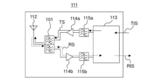
- FIG. 1 is a diagram illustrating a duplexer as an example of a use of an elastic wave resonator according to an embodiment of the present disclosure. 1 is a block diagram showing a configuration of a main part of a communication device as an example of a use of an acoustic wave resonator according to an embodiment of the present disclosure.
- the drawings may be accompanied by an orthogonal coordinate system consisting of an X-axis, a Y-axis, and a Z-axis.
- the X-axis is defined to be parallel to the propagation direction of an elastic wave used as the main resonance among the elastic waves propagating through the piezoelectric layer 2 described later
- the Y-axis is defined to be parallel to the extension direction of the electrode fingers 412 described later
- the Z-axis is defined to be perpendicular to the upper surface 2a of the piezoelectric layer 2 described later.
- the orthogonal coordinate system used in this disclosure is an example, and the X-axis, Y-axis, and Z-axis directions may be defined in directions different from those of the orthogonal coordinate system used in this disclosure.
- the terms upper surface and lower surface may be used with the Z-axis direction being the up-down direction.
- the embodiments of the elastic wave resonator according to the present disclosure are merely illustrative. Therefore, different embodiments may be partially substituted with each other. Also, different embodiments may be partially combined with each other.
- FIG. 1 is a schematic cross-sectional view of an elastic wave resonator 1 according to an embodiment of the present disclosure, taken from the Y-axis direction.
- the elastic wave resonator 1 according to an embodiment of the present disclosure has a piezoelectric layer 2, a support substrate 3, an acoustic reflection layer 5, and an IDT electrode 4.
- the piezoelectric layer 2 has an upper surface 2a and a lower surface 2b perpendicular to the Z axis, with the Z axis being the up-down direction.
- the lower surface 2b is located opposite the upper surface 2a.
- the upper surface 2a may be called the first surface
- the lower surface 2b may be called the second surface.
- An acoustic reflection layer 5 and a support substrate 3, which will be described later, are located on the lower surface 2b side of the piezoelectric layer 2.
- An IDT electrode 4, which will be described later, is located on the upper surface 2a side of the piezoelectric layer 2.
- the piezoelectric layer 2 contains a material having piezoelectricity, such as a single crystal of lithium tantalate (LiTaO 3 , hereinafter referred to as LT) or a single crystal of lithium niobate (LiNbO 3 , hereinafter referred to as LN).
- LT lithium tantalate
- LN lithium niobate
- the piezoelectric layer 2 has piezoelectric properties, and when a high-frequency signal is applied to the IDT electrode 4, an elastic wave propagating through the piezoelectric layer 2 is excited.
- the elastic wave excited as the main resonance is at least one of a plate wave and a bulk wave.
- the type and propagation mode of the plate wave or bulk wave excited as the main resonance are not particularly limited and may be set according to the desired frequency characteristics.
- the Euler angles ( ⁇ , ⁇ , ⁇ ) of the piezoelectric single crystal contained in the piezoelectric layer 2 may be appropriately designed according to the type and propagation mode of the plate wave or bulk wave used as the main resonance.
- Lamb waves and SH waves can be exemplified as types of plate waves.
- the A1 mode which is an asymmetric mode
- the S mode which is a symmetric mode
- the elastic wave excited as the main resonance is the A1 mode of the Lamb wave, which is a plate wave.
- the A1 mode of the Lamb wave can be effectively used as the main resonance by setting the Euler angles ( ⁇ , ⁇ , ⁇ ) of LT to (0° ⁇ 10°, 0° to 55°, 0° ⁇ 10°) or a crystallographically equivalent angle.
- the angles may be (0° ⁇ 10°, 30° ⁇ 10°, 0° ⁇ 10°) or a crystallographically equivalent angle.
- the A1 mode of the Lamb wave can be effectively used as the main resonance by setting the Euler angles ( ⁇ , ⁇ , ⁇ ) of LN to (0° ⁇ 10°, 0° to 55°, 0° ⁇ 10°) or a crystallographically equivalent angle.
- the angles may be (0° ⁇ 10°, 35° ⁇ 10°, 0° ⁇ 10°) or crystallographically equivalent angles.
- the primary resonance refers to the resonance with the smallest minimum impedance value (or, from another point of view, the impedance at the resonant frequency) among multiple resonances with different resonant frequencies that occur in the elastic wave resonator 1.
- a specific elastic wave e.g., a plate wave
- the main component is, for example, a component that occupies 50% or more or 80% or more of the energy of the elastic wave at the resonant frequency.
- both a plate wave and a bulk wave are used as the primary resonance, it is sufficient that the total energy of both has the above-mentioned value (each may be less than the above-mentioned lower limit).
- the thickness of the piezoelectric layer 2 may be ⁇ or less, expressed using a wavelength ⁇ described later. By setting the thickness of the piezoelectric layer 2 to ⁇ or less, at least one of the plate wave and the bulk wave can be effectively used as the main resonance.
- the thickness of the piezoelectric layer 2 may be 0.5 ⁇ or less. In this case, at least one of the plate wave and the bulk wave can be more effectively used as the main resonance. Furthermore, it may be 0.4 ⁇ or less or 0.3 ⁇ or less.
- the piezoelectric layer 2 may be made as thin as possible.
- the thickness of the piezoelectric layer 2 may be 0.05 ⁇ or more, 0.10 ⁇ or more, or 0.15 ⁇ or more. The above lower limit and upper limit may be combined arbitrarily.
- the support substrate 3 is located on the lower surface 2b side of the piezoelectric layer 2.
- the thickness of the support substrate 3 is not particularly limited, and for example, the thickness of the support substrate 3 may be thicker than the thickness of the piezoelectric layer 2.
- the material of the support substrate 3 is not particularly limited.
- the material of the support substrate 3 may be a material having a smaller linear expansion coefficient than that of the piezoelectric layer 2.
- a material for the support substrate 3 it is possible to reduce deformation of the piezoelectric layer 2 due to temperature changes and reduce changes in the resonance characteristics of the elastic wave resonator 1 due to temperature changes.
- materials for such a support substrate 3 include sapphire (Al 2 O 3 ), silicon carbide (SiC), and silicon (Si).
- the acoustic reflection layer 5 is located on the lower surface 2b side of the piezoelectric layer 2 (in direct or indirect contact with it), and is located between the piezoelectric layer 2 and the support substrate 3.
- the acoustic impedance of the acoustic reflection layer 5 is different from the acoustic impedance of the piezoelectric layer 2. In this case, a difference in acoustic impedance occurs between the piezoelectric layer 2 and the acoustic reflection layer 5, so that the excited elastic waves can be effectively trapped in the piezoelectric layer 2.
- the acoustic reflection layer 5 may be composed of one layer or multiple layers.
- the acoustic reflection layer 5 may be composed of multiple low acoustic impedance layers 51 and multiple high acoustic impedance layers 52 alternately stacked.
- the acoustic impedance of the low acoustic impedance layer 51 is smaller than the acoustic impedance of the piezoelectric layer 2.
- the acoustic impedance of the high acoustic impedance layer 52 is larger than the acoustic impedance of the low acoustic impedance layer 51.
- An example of such a low acoustic impedance layer 51 is silicon oxide (SiO 2 ), etc.
- An example of such a high acoustic impedance layer 52 is hafnium oxide (HfO 2 ), tantalum oxide (Ta 2 O 5 ), tungsten (W), molybdenum (Mo), zirconium oxide (ZrO 2 ), etc.
- the IDT electrode 4 is located on the upper surface 2a side of the piezoelectric layer 2.
- the IDT electrode 4 is made of a conductive material.
- the IDT electrode 4 may be made of various conductive materials such as aluminum (Al), copper (Cu), platinum (Pt), molybdenum (Mo), gold (Au), or alloys thereof.
- the IDT electrode 4 may be made by laminating multiple layers of various conductive materials as described above. When the IDT electrode 4 is made by laminating multiple layers, a diffusion prevention layer made of a metal such as titanium (Ti) or a dielectric may be interposed at the lamination interface.
- the layer located on the side of the piezoelectric layer 2 may be a base layer made of a metal such as titanium (Ti) or a dielectric.
- the IDT electrode 4 is Al.
- the IDT electrode 4 has a comb-shaped electrode 41.
- the comb-shaped electrode 41 includes a plurality of arranged electrode fingers 412.
- the comb-shaped electrode 41 also includes a pair of bus bars 411 that are positioned in a direction intersecting the arrangement direction of the plurality of electrode fingers 412 and are connected to the plurality of electrode fingers 412. In other words, the plurality of electrode fingers 412 extend from the bus bar 411.
- the plurality of electrode fingers 412 are arranged such that the plurality of electrode fingers 412a connected to one bus bar 411a and the electrode fingers 412b connected to the other bus bar 411b interdigitate with each other.
- the arrangement direction of the plurality of electrode fingers 412 is the X-axis direction
- the extension direction of the plurality of electrode fingers 412 is the Y-axis direction.
- the comb-shaped electrode 41 may include a plurality of dummy electrode fingers 413 located between each of the plurality of electrode fingers 412.
- the plurality of dummy electrode fingers 413 include a plurality of dummy electrode fingers 413a connected to one bus bar 411a and facing the electrode fingers 412b extending from the other bus bar 411b, and a plurality of dummy electrode fingers 413b connected to one bus bar 411b and facing the electrode fingers 412a extending from the other bus bar 411a.
- “facing” does not necessarily require that the opposing surfaces are parallel to each other, and the opposing surfaces may be inclined.
- the length of the electrode fingers 412 in the extension direction may be set appropriately depending on the required electrical characteristics, etc. For example, the lengths of the electrode fingers 412 in the extension direction are equal to each other.
- the IDT electrode 4 may be apodized, in which the length of the electrode fingers 412 in the extension direction changes depending on the position in the X-axis direction.
- the repeat interval in the arrangement direction of the multiple electrode fingers 412 is defined as pitch P.
- the pitch P is appropriately designed according to the desired frequency characteristics.
- the pitch P is constant, but is not limited to this example.
- the pitch P may be designed to gradually increase, or may be designed to have multiple types of repeat intervals in stages. If there are multiple different repeat intervals, the average value of the repeat intervals measured at 5 to 10 locations may be defined as the pitch P, or the largest repeat interval may be defined as the pitch P.
- the specific value of the pitch P is arbitrary.
- the pitch P may be 0.5 ⁇ m or more or 1 ⁇ m or more, and may be 10 ⁇ m or less, 5 ⁇ m or less, or 2 ⁇ m or less.
- the above lower limit examples and upper limit examples may be combined arbitrarily.
- the pitch P of the electrode fingers 412 is 1.1 ⁇ m.
- an elastic wave with a wavelength ⁇ defined as twice the pitch P which is the repeating interval of the multiple electrode fingers 412, is excited and propagates through the piezoelectric layer 2.
- the wavelength ⁇ may have low dependency on the pitch P, as in the case of a bulk wave that propagates in the thickness direction of the piezoelectric layer 2.
- ⁇ when defining the thickness of the piezoelectric layer 2, etc. only needs to be twice the pitch P, and may deviate from the wavelength of the elastic wave excited as the main resonance.
- the elastic wave resonator 1 in one embodiment of the present disclosure may further include (or may not include) a pair of reflectors 42 located on the upper surface 2a side of the piezoelectric layer 2.
- the pair of reflectors 42 are located on both sides of the comb-shaped electrode 41 in the X-axis direction.
- the reflector 42 includes a pair of reflector bus bars 421 facing each other and a plurality of strip electrodes 422 extending between the pair of reflector bus bars 421.
- FIGS. 3A and 3B are schematic cross-sectional views of an elastic wave resonator 1 according to an embodiment of the present disclosure taken in the Y-axis direction, with the electrode fingers 412 enlarged.
- FIGS. 3A and 3B are cross-sectional views taken in the direction in which the electrode fingers 412 extend.
- the piezoelectric layer 2 has a groove 21 on the upper surface 2a. At least a portion of the electrode fingers 412 is located in the groove 21. All of the electrode fingers 412 may be located in the groove 21, but this is not limited to this example. For example, the electrode fingers 412 located in the groove 21 and the electrode fingers 412 located outside the groove 21 may coexist. The entire thickness (and/or volume) of the electrode fingers 412 located in the groove 21 may be located in the groove 21. This is also not limited to this example. For example, it is sufficient that at least a portion (e.g., the lower portion) of the thickness (and/or volume) of the electrode fingers 412 is located in the groove 21. The region of the electrode fingers 412 located in the groove 21 may be called the embedded region 45 to distinguish it from the protruding region 46 described later.
- the embedded region 45 located in the groove 21 of the electrode finger 412 has a wide region 43 and a narrow region 44.
- the width of the electrode finger 412 in the narrow region 44 is narrower than the width of the electrode finger 412 in the wide region 43.
- T1 may be the width of any part of the wide region 43
- T2 may be the width of any part of the narrow region 44.
- T1 may be the width of the widest part of the wide region 43
- T2 may be the width of the narrowest part of the narrow region 44.
- the "width" of the electrode finger 412 is the length of the electrode finger 412 in the X-axis direction.
- the narrow region 44 is an area narrower than the narrowest part of the wide region 43
- the wide region 43 is an area wider than the widest part of the narrow region 44.
- the entire wide region 43 is wider than the entire narrow region 44
- the entire narrow region 44 is narrower than the entire wide region 43.
- the embedded region 45 of the electrode finger 412 may have multiple wide regions 43 or multiple narrow regions 44.
- the specific cross-sectional shape of the electrode fingers 412 in one embodiment of the present disclosure from the extension direction is a trapezoid with the main surface located on the opening side of the groove 21 as the upper base 451, the main surface located on the bottom side of the groove 21 as the lower base 452, and the side surfaces as the legs 453.
- the cross-sectional shape of the electrode fingers 412 from the extension direction is trapezoidal, the narrow region 44 is located closer to the lower surface 2b of the piezoelectric layer 2 than the wide region 43.
- the pitch P1 of the electrode fingers 412 in the wide region 43 and the pitch P2 of the electrode fingers 412 in the narrow region 44 can be made different.
- the aforementioned pitch P is a parameter that is not affected by the width of the electrode fingers 412, and is, for example, the center-to-center distance between adjacent electrode fingers 412.
- the pitches P1 and P2 are parameters that are affected by the width of the electrode fingers 412, and are, for example, the distance (spacing) between the side surfaces of adjacent electrode fingers 412.
- the pitch (e.g., P1 and P2) of the electrode fingers 412 differs in the thickness direction, it becomes difficult for the main mode, which is the main resonance, and the spurious mode, which is an unwanted wave, to resonate, and the phase intensity of both is reduced.
- at least one of plate waves and bulk waves, whose frequency characteristics are less affected by the difference in pitch is used as the main resonance, so that even if the pitch P1 of the electrode fingers 412 in the wide region 43 and the pitch P2 of the electrode fingers 412 in the narrow region 44 are different, the effect on the frequency characteristics of the main resonance can be reduced. Therefore, according to one embodiment of the present disclosure, it is possible to effectively reduce spurious while maintaining good frequency characteristics of the main resonance.
- T1/P and/or T2/P may be 0.05 or more, 0.2 or more, or 0.3 or more, and may be 0.6 or less, 0.5 or less, or 0.3 or less, and the above lower and upper limits may be combined with any values so as not to cause a contradiction.
- the thickness of the electrode finger 412 and/or the depth of the groove 21 may be 0.005 ⁇ or more, 0.01 ⁇ or more, 0.02 ⁇ or more, or 0.04 ⁇ or more, provided that they are equal to or less than the thickness of the piezoelectric layer 2 (or less than the thickness of the piezoelectric layer 2), and may be 0.5 ⁇ or less, 0.3 ⁇ or less, or 0.1 ⁇ or less, and the above lower and upper limits may be combined with any values.
- the thicker the electrode fingers 412 the easier it is to achieve the above-mentioned structure and effects of the electrode fingers 412.
- FIG. 4 shows the simulation results of the frequency characteristics of the elastic wave resonator 1 according to one embodiment of the present disclosure.
- the solid line shows the simulation results of Example 1 shown in FIGS. 1 and 3, and the dotted line shows the simulation results of the comparative example.
- Example 1 the side surfaces of the electrode fingers 412 are inclined as shown in FIG. 3, and the cross-sectional shape of the embedded region 45 of the electrode fingers 412 is trapezoidal.
- the side surfaces of the electrode fingers 412 are not inclined, and the cross-sectional shape of the embedded region 45 is rectangular.
- FIGS. 5A to 5C show an elastic wave resonator 1 according to another example of the present disclosure.
- the narrow region 44 is located closer to the bottom surface 2b of the piezoelectric layer 2 than the wide region 43, but this is not limiting.
- the narrow region 44 is located closer to the top surface 2a of the piezoelectric layer 2 than the wide region 43.
- the cross-sectional shape of the embedded region 45 of the electrode finger 412 is trapezoidal with the main surface located on the bottom side of the groove 21 as the bottom base and the side surfaces as the legs, but this is not limited to this example.
- the cross-sectional shape of the embedded region 45 of the electrode finger 412 is a combination of a rectangular wide region 43 and a rectangular narrow region 44. Note that in the example shown in FIG. 5B, the narrow region 44 is located closer to the bottom surface 2b of the piezoelectric layer 2 than the wide region 43.
- the electrode finger 412 shows an example in which the entire electrode finger 412 is located within the groove 21, but this is not limiting.
- part of the electrode finger 412 may be located within the groove 21 and part may be located outside the groove 21.
- the region of the electrode finger 412 that is located outside the groove 21 is defined as the protruding region 46.
- the width of the protruding region 46 can be set as appropriate.
- the width of the protruding region 46 may be larger or smaller than the width of the narrow region 44 in the embedded region 45.
- the length of the protruding region 46 in the Z-axis direction may be smaller than the length of the buried region 45 in the Z-axis direction.
- the amount of protrusion from the piezoelectric layer 2 in the protruding region 46 may be smaller than the amount of embedding in the buried region 45. In this case, the spurious reduction effect in the buried region 45 is more effectively achieved.
- a gap 53 may be located between the piezoelectric layer 2 and the support substrate 3.
- a gas is present in the gap 53.
- the gas may be air or an inert gas such as nitrogen or argon.
- the support substrate 3 may be in direct or indirect contact with the piezoelectric layer 2.
- the void 53 is located at a position where it overlaps with the multiple electrode fingers 412 when viewed from a plan view in the Z-axis direction. With this configuration, the gas present in the void 53 acts as an acoustic reflection layer, effectively reducing the leakage of elastic waves from the lower surface 2b of the piezoelectric layer 2.
- the size and depth of the void 53 may be set as appropriate.
- the angle ⁇ between the upper base 451 and the legs 453 may be any value less than 90°.
- the larger the angle ⁇ the greater the difference in width between the electrode fingers 412 in the wide region 43 and the electrode fingers 412 in the narrow region 44.
- the difference between the pitch P1 of the electrode fingers 412 in the wide region 43 and the pitch P2 of the electrode fingers 412 in the narrow region 44 also becomes larger, so that spurious can be reduced more effectively.
- the angle ⁇ between the upper base 451 and the leg 453 may be in the range of more than 35° and less than 90°.
- Figures 7A and 7B are diagrams showing simulation results of frequency characteristics when the angle ⁇ is changed for Example 1 and Example 2, which are an embodiment of the present disclosure.
- the vertical axis of Figures 7A and 7B indicates the fractional bandwidth ⁇ f (%) of the main resonance, and the horizontal axis indicates the angle ⁇ (°).
- the fractional bandwidth ⁇ f is defined as (fa-fr) x 100/fr, where fr is the resonant frequency of the elastic wave resonator 1 and fa is the anti-resonant frequency.
- fr the resonant frequency of the elastic wave resonator 1
- fa is the anti-resonant frequency.
- the larger the fractional bandwidth ⁇ f of the main resonance the larger the band as a filter and the improved frequency characteristics.
- FIG. 7A shows the results of a simulation of the frequency characteristics of Example 1.
- FIG. 7B shows the results of a simulation of the frequency characteristics of Example 2.
- Example 1 is an embodiment shown in FIG. 1, in which an acoustic reflection layer 5 consisting of a low acoustic impedance layer 51 and a high acoustic impedance layer 52 laminated together is present on the lower surface 2b side of the piezoelectric layer 2.
- Example 2 is an embodiment shown in FIG. 6, in which a gap 53 is present on the lower surface 2b side of the piezoelectric layer 2.
- the piezoelectric layers 2 in both Examples 1 and 2 are LT. Design details for Examples 1 and 2 are shown below.
- Example 1 (low acoustic impedance layer: SiO 2 , high acoustic impedance layer: HfO 2 )
- Example 2 (with gaps) The angle ⁇ was changed by changing the width T2 while keeping the width T1 and the electrode thickness constant.
- the angle ⁇ may be in the range greater than 35° and less than 85°. In this case, the bandwidth ratio ⁇ f can be increased even more effectively.
- the angle ⁇ may be in the range greater than 35° and less than 80°. In this case, the bandwidth ratio ⁇ f can be increased even more effectively.
- the angle ⁇ may be in the range greater than 35° and less than 70°. In this case, the bandwidth ratio ⁇ f can be increased even more effectively.
- the angle ⁇ between the upper base 451 and the leg 453 may be in the range of more than 45° and less than 90°.
- 8A and 8B are diagrams showing simulation results of frequency characteristics when the angle ⁇ is changed for Example 1 and Example 2, which are an embodiment of the present disclosure.
- the vertical axis of FIG. 8A and FIG. 8B indicates the peak-valley PV value of the main resonance, and the horizontal axis indicates the angle ⁇ (°).
- PV is defined as the value obtained by dividing the absolute value
- PV is defined as (
- FIG. 8A shows the simulation results of the frequency characteristics of Example 1.
- FIG. 8B shows the simulation results of the frequency characteristics of Example 2.
- the angle ⁇ may be in the range greater than 45° and less than 85°. In this case, the PV can be increased even more effectively.
- the angle ⁇ may be in the range greater than 45° and less than 80°. In this case, the PV can be increased even more effectively.
- the angle ⁇ may be in the range greater than 45° and less than 70°. In this case, the PV can be increased even more effectively.
- Figures 9A and 9B are diagrams showing simulation results of frequency characteristics when the angle ⁇ is changed for Example 3 and Example 4, which are an embodiment of the present disclosure.
- the vertical axis of Figures 9A and 9B indicates the fractional bandwidth ⁇ f (%) of the main resonance, and the horizontal axis indicates the angle ⁇ (°).
- FIG. 9A shows the results of a simulation of the frequency characteristics of Example 3.
- FIG. 9B shows the results of a simulation of the frequency characteristics of Example 4.
- Example 3 is an embodiment shown in FIG. 1, in which an acoustic reflection layer 5 consisting of a low acoustic impedance layer 51 and a high acoustic impedance layer 52 laminated together is present on the lower surface 2b side of the piezoelectric layer 2.
- Example 4 is an embodiment shown in FIG. 6, in which a gap 53 is present on the lower surface 2b side of the piezoelectric layer 2.
- the piezoelectric layer 2 in both Examples 3 and 4 is LN. Design details for Examples 3 and 4 are provided below.
- Example 3 (piezoelectric layer: LN, piezoelectric layer Euler angles: (0°, 35°, 0°), piezoelectric layer thickness: 0.37 ⁇ m, IDT electrode: Al, pitch P: 1.1 ⁇ m, T1/P: 0.5, electrode thickness: 0.11 ⁇ m, support substrate: Si)
- Example 3 (low acoustic impedance layer: SiO 2 , high acoustic impedance layer: HfO 2 )
- Example 4 (with voids) The angle ⁇ was changed by changing the width T2 while keeping the width T1 and the electrode thickness constant.
- the angle ⁇ may be in the range greater than 55° and less than 85°. In this case, the bandwidth ratio ⁇ f can be increased even more effectively.
- the angle ⁇ may be in the range greater than 55° and less than 80°. In this case, the bandwidth ratio ⁇ f can be increased even more effectively.
- the angle ⁇ may be in the range greater than 55° and less than 70°. In this case, the bandwidth ratio ⁇ f can be increased even more effectively.
- the angle ⁇ between the upper base 451 and the leg 453 may be in the range of greater than 45° and less than 90°.
- Figures 10A and 10B are diagrams showing simulation results of frequency characteristics when the angle ⁇ is changed for Example 3 and Example 4, which are an embodiment of the present disclosure.
- the vertical axis of Figures 10A and 10B shows the PV value of the main resonance, and the horizontal axis shows the angle ⁇ (°).
- FIG. 10A shows the simulation results of the frequency characteristics of Example 3.
- FIG. 10B shows the simulation results of the frequency characteristics of Example 4.
- the angle ⁇ may be in the range greater than 45° and less than 85°. In this case, the PV can be increased even more effectively.
- the angle ⁇ may be in the range greater than 45° and less than 80°. In this case, the PV can be increased even more effectively.
- the angle ⁇ may be in the range greater than 45° and less than 70°. In this case, the PV can be increased even more effectively.
- a "trapezoid” does not necessarily have to be a trapezoid in the strict sense.
- each corner of the trapezoid may be rounded.
- the upper base, lower base, and legs do not necessarily have to be strictly straight lines.
- the upper base, lower base, and legs may be rounded curves.
- the angle ⁇ between the upper base and the legs may be calculated as, for example, the angle between the tangent at the midpoint of the upper base and the tangent at the midpoint of the legs.
- the angle ⁇ between the upper base and the leg may be determined, for example, as the angle between a line that roughly overlaps the part of the upper base excluding the partial concave or convex part, and a line that roughly overlaps the part of the leg excluding the partial concave or convex part.
- the cross-sectional shape of the electrode fingers 412 can be realized by various methods. For example, a groove 21 is formed in the piezoelectric layer 2, and the cross-sectional shape of the groove 21 is made into a desired shape such as a trapezoid. Next, a metal layer that becomes the electrode fingers 412 is formed. At this time, the metal layer fills the groove 21, so that the cross-sectional shape of the electrode fingers 412 becomes the same as the cross-sectional shape of the groove 21, and thus becomes a desired shape such as a trapezoid. There are various methods for forming the groove 21 having a desired cross-sectional shape. For example, the groove 21 may be formed by etching (e.g., wet etching).
- the anisotropy of a single crystal with respect to etching may be utilized, or etching with different conditions may be performed sequentially, thereby realizing a cross-sectional shape such as a trapezoid.
- the groove 21 may be formed by laser processing. Then, a tapered or inverse tapered shape of laser light may be utilized, or etching with different conditions may be performed sequentially, thereby realizing a cross-sectional shape such as a trapezoid.
- FIG. 11 is a circuit diagram showing a schematic configuration of a duplexer 101 as an example of the use of the elastic wave resonator 1.
- the comb-shaped electrode 41 is shown typically in a bifurcated fork shape, and the reflector 42 is represented by a single line bent at both ends.
- the splitter 101 has, for example, a transmit filter 105 that filters the transmit signal from the transmit terminal 103 and outputs it to the antenna terminal 102, and a receive filter 106 that filters the receive signal from the antenna terminal 102 and outputs it to the receive terminal 104.
- the transmit filter 105 and the receive filter 106 are configured, for example, as ladder-type filters in which multiple resonators are connected in a ladder configuration. That is, the transmit filter 105 has one or more series resonators connected in series between the transmit terminal 103 and the antenna terminal 102, and one or more parallel resonators that connect the series arm to a reference potential.
- the elastic wave resonator 1 in one embodiment of the present disclosure may be used as at least one of the series resonators or parallel resonators in the transmit filter 105 and the receive filter 106.
- FIG. 11 is merely one example of the configuration of the splitter 101, and the splitter 101 is not limited to the configuration in FIG. 11.
- the transmit filter 105 may be configured as a multimode filter.
- both the transmit filter 105 and the receive filter 106 are elastic wave filters, but this configuration is not limiting.
- either the transmit filter 105 or the receive filter 106 may be an elastic wave filter that uses an elastic wave resonator 1, and the other may be an LC filter that includes one or more inductors and one or more capacitors.
- splitter 101 includes transmit filter 105 and receive filter 106
- splitter 101 is not limited to this configuration.
- splitter 101 may be a diplexer or a multiplexer including three or more filters.
- (Example of use of elastic wave resonator 1: communication device) 12 is a block diagram showing a main part of a communication device 111 as an example of a use of the acoustic wave resonator 1 and the duplexer 101.
- the communication device 111 includes the duplexer 101, and performs wireless communication using radio waves.
- a transmission information signal TIS containing information to be transmitted is modulated and frequency-raised by an RF-IC (Radio Frequency Integrated Circuit) 113 to produce a transmission signal TS.
- RF-IC Radio Frequency Integrated Circuit
- Unnecessary components outside the transmission passband are removed from the transmission signal TS by a bandpass filter 115a, amplified by an amplifier 114a, and input to the transmission terminal 103.
- the transmission filter 105 then removes unnecessary components outside the transmission passband from the input transmission signal TS, and outputs the removed transmission signal TS from the antenna terminal 102 to the antenna 112.
- the antenna 112 converts the input transmission signal TS into a radio signal and transmits it.
- a radio signal received by the antenna 112 is converted by the antenna 112 into a received signal RS and input to the antenna terminal 102.
- the receiving filter 106 removes unnecessary components outside the receiving passband from the input received signal RS and outputs it from the receiving terminal 104 to the amplifier 114b.
- the output received signal RS is amplified by the amplifier 114b, and unnecessary components outside the receiving passband are removed by the bandpass filter 115b.
- the received signal RS is then frequency-downshifted and demodulated by the RF-IC 113 to become a received information signal RIS.
- the transmitted information signal TIS and the received information signal RIS may be low-frequency signals containing appropriate information, for example, analog audio signals or digitized audio signals.
- the passband of the wireless signal may be set as appropriate, and in one embodiment of the present disclosure, a relatively high-frequency passband is also possible.
- the modulation method may be any of phase modulation, amplitude modulation, frequency modulation, or a combination of two or more of these.
- the circuit method in FIG. 12 illustrates a direct conversion method, it is not limited to this example and may be, for example, a double superheterodyne method. Also, FIG. 12 shows only the essential parts in a schematic manner, and a low-pass filter or an isolator may be added at an appropriate position, and the position of an amplifier, etc. may be changed.
- Elastic wave resonator 2 Piezoelectric layer 2a: Upper surface (first surface) 2b: Bottom surface (second surface) 21: Groove 3: Support substrate 4: IDT electrode 41: Comb-shaped electrode 411: Bus bar 412: Electrode finger (first electrode finger) 42: Reflector 43: Wide region 44: Narrow region 45: Buried region 46: Protruding region 451: Upper base 452: Lower base 453: Leg 5: Acoustic reflecting layer 51: Low acoustic impedance layer 52: High acoustic impedance layer 53: Air gap 101: Splitter 102: Antenna terminal 103: Transmitting terminal 104: Receiving terminal 111: Communication device 112: Antenna 113: RF-IC 114: Amplifier 115: Bandpass filter
Landscapes
- Physics & Mathematics (AREA)
- Acoustics & Sound (AREA)
- Piezo-Electric Or Mechanical Vibrators, Or Delay Or Filter Circuits (AREA)
- Surface Acoustic Wave Elements And Circuit Networks Thereof (AREA)
Priority Applications (2)
| Application Number | Priority Date | Filing Date | Title |
|---|---|---|---|
| JP2025516774A JPWO2024225181A1 (https=) | 2023-04-25 | 2024-04-19 | |
| CN202480027089.2A CN121002774A (zh) | 2023-04-25 | 2024-04-19 | 弹性波共振子和通信装置 |
Applications Claiming Priority (2)
| Application Number | Priority Date | Filing Date | Title |
|---|---|---|---|
| JP2023071664 | 2023-04-25 | ||
| JP2023-071664 | 2023-04-25 |
Publications (1)
| Publication Number | Publication Date |
|---|---|
| WO2024225181A1 true WO2024225181A1 (ja) | 2024-10-31 |
Family
ID=93256318
Family Applications (1)
| Application Number | Title | Priority Date | Filing Date |
|---|---|---|---|
| PCT/JP2024/015526 Ceased WO2024225181A1 (ja) | 2023-04-25 | 2024-04-19 | 弾性波共振子および通信装置 |
Country Status (3)
| Country | Link |
|---|---|
| JP (1) | JPWO2024225181A1 (https=) |
| CN (1) | CN121002774A (https=) |
| WO (1) | WO2024225181A1 (https=) |
Citations (5)
| Publication number | Priority date | Publication date | Assignee | Title |
|---|---|---|---|---|
| WO2011018913A1 (ja) * | 2009-08-10 | 2011-02-17 | 株式会社村田製作所 | 弾性境界波装置 |
| WO2012086441A1 (ja) * | 2010-12-24 | 2012-06-28 | 株式会社村田製作所 | 弾性波装置及びその製造方法 |
| JP2012257019A (ja) * | 2011-06-08 | 2012-12-27 | Murata Mfg Co Ltd | 弾性波装置 |
| WO2014054580A1 (ja) * | 2012-10-05 | 2014-04-10 | 株式会社村田製作所 | 弾性表面波装置 |
| JP2019062441A (ja) * | 2017-09-27 | 2019-04-18 | 株式会社村田製作所 | 弾性波装置 |
-
2024
- 2024-04-19 CN CN202480027089.2A patent/CN121002774A/zh active Pending
- 2024-04-19 WO PCT/JP2024/015526 patent/WO2024225181A1/ja not_active Ceased
- 2024-04-19 JP JP2025516774A patent/JPWO2024225181A1/ja active Pending
Patent Citations (5)
| Publication number | Priority date | Publication date | Assignee | Title |
|---|---|---|---|---|
| WO2011018913A1 (ja) * | 2009-08-10 | 2011-02-17 | 株式会社村田製作所 | 弾性境界波装置 |
| WO2012086441A1 (ja) * | 2010-12-24 | 2012-06-28 | 株式会社村田製作所 | 弾性波装置及びその製造方法 |
| JP2012257019A (ja) * | 2011-06-08 | 2012-12-27 | Murata Mfg Co Ltd | 弾性波装置 |
| WO2014054580A1 (ja) * | 2012-10-05 | 2014-04-10 | 株式会社村田製作所 | 弾性表面波装置 |
| JP2019062441A (ja) * | 2017-09-27 | 2019-04-18 | 株式会社村田製作所 | 弾性波装置 |
Also Published As
| Publication number | Publication date |
|---|---|
| JPWO2024225181A1 (https=) | 2024-10-31 |
| CN121002774A (zh) | 2025-11-21 |
Similar Documents
| Publication | Publication Date | Title |
|---|---|---|
| CN111953309B (zh) | 表面声波元件、滤波电路以及电子零件 | |
| JP6856825B2 (ja) | 弾性波装置、分波器および通信装置 | |
| US20220014172A1 (en) | Elastic wave device, splitter, and communication apparatus | |
| JP4552931B2 (ja) | 弾性波デバイスおよびそれを用いた移動体通信機器並びにセンサー | |
| CN102422534B (zh) | 天线共用器 | |
| JP7278305B2 (ja) | 弾性波装置、分波器および通信装置 | |
| EP1732216B1 (en) | Surface acoustic device | |
| CN112929004B (zh) | 声波谐振器、滤波器、多路复用器和晶片 | |
| JP6284800B2 (ja) | 弾性表面波デバイス及びフィルタ | |
| JP2022075959A (ja) | 弾性波フィルタ | |
| JP6760480B2 (ja) | エクストラクタ | |
| JP7433216B2 (ja) | 弾性波素子、弾性波フィルタ、分波器および通信装置 | |
| JP2002314366A (ja) | 弾性表面波フィルタ、弾性表面波装置および通信装置 | |
| WO2019017422A1 (ja) | マルチプレクサ、高周波フロントエンド回路および通信装置 | |
| JP4100249B2 (ja) | 弾性表面波装置、通信機 | |
| JP2015109574A (ja) | 縦結合共振子型弾性表面波フィルタおよび通信機 | |
| JP7793060B2 (ja) | 弾性波共振子、弾性波フィルタおよび通信装置 | |
| JP7519902B2 (ja) | Sawフィルタデバイスにおける発生源抑制のための変換器構造 | |
| JP7678241B1 (ja) | 弾性波装置、通信装置、圧電基板 | |
| US20250105822A1 (en) | Filter device, splitter, and communication device | |
| JP2025003073A (ja) | フィルタデバイスおよび通信装置 | |
| US20240356522A1 (en) | Elastic wave element, demultiplexer, and communication device | |
| WO2024225181A1 (ja) | 弾性波共振子および通信装置 | |
| JP7431702B2 (ja) | 弾性波デバイス、通信装置及び弾性波デバイスの製造方法 | |
| WO2024190677A1 (ja) | 弾性波共振子および通信装置 |
Legal Events
| Date | Code | Title | Description |
|---|---|---|---|
| 121 | Ep: the epo has been informed by wipo that ep was designated in this application |
Ref document number: 24796928 Country of ref document: EP Kind code of ref document: A1 |
|
| ENP | Entry into the national phase |
Ref document number: 2025516774 Country of ref document: JP Kind code of ref document: A |
|
| WWE | Wipo information: entry into national phase |
Ref document number: 2025516774 Country of ref document: JP |
|
| NENP | Non-entry into the national phase |
Ref country code: DE |
|
| 122 | Ep: pct application non-entry in european phase |
Ref document number: 24796928 Country of ref document: EP Kind code of ref document: A1 |