WO2024224724A1 - フィルタ装置、およびアンテナ装置 - Google Patents
フィルタ装置、およびアンテナ装置 Download PDFInfo
- Publication number
- WO2024224724A1 WO2024224724A1 PCT/JP2024/002365 JP2024002365W WO2024224724A1 WO 2024224724 A1 WO2024224724 A1 WO 2024224724A1 JP 2024002365 W JP2024002365 W JP 2024002365W WO 2024224724 A1 WO2024224724 A1 WO 2024224724A1
- Authority
- WO
- WIPO (PCT)
- Prior art keywords
- inductor
- filter device
- external electrode
- capacitor
- pattern
- Prior art date
- Legal status (The legal status is an assumption and is not a legal conclusion. Google has not performed a legal analysis and makes no representation as to the accuracy of the status listed.)
- Ceased
Links
Images




Classifications
-
- H—ELECTRICITY
- H03—ELECTRONIC CIRCUITRY
- H03H—IMPEDANCE NETWORKS, e.g. RESONANT CIRCUITS; RESONATORS
- H03H7/00—Multiple-port networks comprising only passive electrical elements as network components
- H03H7/01—Frequency selective two-port networks
- H03H7/17—Structural details of sub-circuits of frequency selective networks
- H03H7/1741—Comprising typical LC combinations, irrespective of presence and location of additional resistors
- H03H7/175—Series LC in series path
-
- H—ELECTRICITY
- H01—ELECTRIC ELEMENTS
- H01P—WAVEGUIDES; RESONATORS, LINES, OR OTHER DEVICES OF THE WAVEGUIDE TYPE
- H01P1/00—Auxiliary devices
- H01P1/20—Frequency-selective devices, e.g. filters
-
- H—ELECTRICITY
- H03—ELECTRONIC CIRCUITRY
- H03H—IMPEDANCE NETWORKS, e.g. RESONANT CIRCUITS; RESONATORS
- H03H7/00—Multiple-port networks comprising only passive electrical elements as network components
- H03H7/01—Frequency selective two-port networks
- H03H7/0115—Frequency selective two-port networks comprising only inductors and capacitors
-
- H—ELECTRICITY
- H03—ELECTRONIC CIRCUITRY
- H03H—IMPEDANCE NETWORKS, e.g. RESONANT CIRCUITS; RESONATORS
- H03H7/00—Multiple-port networks comprising only passive electrical elements as network components
- H03H7/01—Frequency selective two-port networks
- H03H7/09—Filters comprising mutual inductance
-
- H—ELECTRICITY
- H03—ELECTRONIC CIRCUITRY
- H03H—IMPEDANCE NETWORKS, e.g. RESONANT CIRCUITS; RESONATORS
- H03H7/00—Multiple-port networks comprising only passive electrical elements as network components
- H03H7/01—Frequency selective two-port networks
- H03H7/17—Structural details of sub-circuits of frequency selective networks
- H03H7/1741—Comprising typical LC combinations, irrespective of presence and location of additional resistors
- H03H7/1758—Series LC in shunt or branch path
-
- H—ELECTRICITY
- H03—ELECTRONIC CIRCUITRY
- H03H—IMPEDANCE NETWORKS, e.g. RESONANT CIRCUITS; RESONATORS
- H03H7/00—Multiple-port networks comprising only passive electrical elements as network components
- H03H7/01—Frequency selective two-port networks
- H03H7/17—Structural details of sub-circuits of frequency selective networks
- H03H7/1741—Comprising typical LC combinations, irrespective of presence and location of additional resistors
- H03H7/1775—Parallel LC in shunt or branch path
-
- H—ELECTRICITY
- H03—ELECTRONIC CIRCUITRY
- H03H—IMPEDANCE NETWORKS, e.g. RESONANT CIRCUITS; RESONATORS
- H03H9/00—Networks comprising electromechanical or electro-acoustic elements; Electromechanical resonators
- H03H9/70—Multiple-port networks for connecting several sources or loads, working on different frequencies or frequency bands, to a common load or source
- H03H9/72—Networks using surface acoustic waves
- H03H9/725—Duplexers
-
- H—ELECTRICITY
- H03—ELECTRONIC CIRCUITRY
- H03H—IMPEDANCE NETWORKS, e.g. RESONANT CIRCUITS; RESONATORS
- H03H1/00—Constructional details of impedance networks whose electrical mode of operation is not specified or applicable to more than one type of network
- H03H2001/0021—Constructional details
- H03H2001/0085—Multilayer, e.g. LTCC, HTCC, green sheets
Definitions
- This disclosure relates to a filter device and an antenna device.
- a filter device such as a band-rejection filter or a band-pass filter is provided in a high-frequency circuit.
- a filter device provided in a high-frequency circuit is disclosed in Japanese Patent No. 6531824 (Patent Document 1).
- the filter device includes a first inductor and a first capacitor that form a first series circuit, and a second inductor that is connected in parallel to the first series circuit.
- Patent Document 1 when the attenuation band (attenuation pole) due to parallel resonance and the pass band due to series resonance are brought close to each other, it is difficult to maintain high attenuation and pass characteristics.
- the present disclosure has been made to solve these problems, and its purpose is to provide a filter device that can obtain good characteristics even when the attenuation band due to parallel resonance and the pass band due to series resonance are close to each other.
- the filter device is a filter device having an attenuation band.
- the filter device includes a first terminal, a second terminal, a first inductor connected to the first terminal, and a series resonator arranged in the first path of a first path and a second path provided in parallel between the first inductor and the second terminal.
- the series resonator includes a second inductor, a capacitor connected in series with the second inductor, and a third inductor connected in series with the second inductor and the capacitor.
- the magnetic coupling between the first inductor and the third inductor is weaker than the magnetic coupling between the first inductor and the second inductor.
- the antenna device is an antenna device capable of radiating radio waves. It comprises an antenna device, a radiating element, a power supply circuit that supplies a high-frequency signal to the radiating element, and the above-mentioned filter device that is provided between the antenna and the power supply circuit.
- a series resonator is disposed in the first path, and the first inductor and the second inductor are configured to be magnetically coupled to each other, so that high attenuation and pass characteristics can be obtained even when the attenuation band due to parallel resonance and the pass band due to series resonance are close to each other.
- FIG. 1 is a perspective view of a filter device according to a first embodiment.
- 1 is a circuit diagram of a filter device and an antenna device according to a first embodiment;
- 10A and 10B are diagrams illustrating attenuation characteristics of a filter device.
- 1 is an exploded plan view showing a configuration of a filter device according to a first embodiment.
- FIG. 11 is a perspective view of a filter device according to a second embodiment.
- FIG. 11 is an exploded plan view showing the configuration of a filter device according to a second embodiment.
- 10 is a graph showing the attenuation characteristics of a filter device according to a second embodiment.
- FIG. 11 is a perspective view of a filter device according to a third embodiment.
- FIG. 11 is an exploded plan view showing the configuration of a filter device according to a third embodiment.
- 13 is a graph showing the attenuation characteristics of a filter device according to a third embodiment.
- FIG. 11 is a circuit diagram of an antenna device according to a first modified example.
- FIG. 11 is a circuit diagram of an antenna device according to a second modified example.
- FIG. 11 is a circuit diagram of an antenna device according to a third modified example.
- Fig. 1 is a perspective view of a filter device 100 according to a first embodiment.
- the short side direction of the filter device 100 is the X direction
- the long side direction is the Y direction
- the height direction is the Z direction.
- the filter device 100 is a rectangular parallelepiped chip component in which two inductors and one capacitor are stacked in the Z direction.
- the filter device 100 is composed of an insulator 3 in which multiple insulating substrates (insulator layers) are stacked on top of each other, on which the first conductor pattern of the first inductor L1, the second conductor pattern of the second inductor L2, and the electrode pattern of the capacitor C1 are formed.
- the stacking direction of the insulating substrates is the Z direction, and the direction of the arrow indicates the upward direction.
- the insulating substrate is made of materials such as an insulating material mainly composed of borosilicate glass, or insulating resins such as alumina, zirconia, and polyimide resin. Furthermore, the interfaces between the multiple insulating substrates in the insulator 3 may not be clear due to processes such as baking and hardening.
- an external electrode 4a first external electrode
- an external electrode 4b second external electrode
- the insulator 3 has a pair of main surfaces that face each other, and the lower main surface in FIG. 1 is the mounting surface, which faces the circuit board.
- the lower main surface in FIG. 1 is also called the bottom surface
- the upper main surface in FIG. 1 is also called the top surface.
- the external electrodes 4a and 4b have electrode patterns formed not only on the bottom surface of the insulator 3, but also on the side surfaces connecting the main surfaces of the insulator 3.
- the external electrodes 4a and 4b are U-shaped. Therefore, the external electrodes 4a provided on each of the opposing side surfaces (first side surface and second side surface) of the insulator 3 are at the same potential due to the electrode pattern provided on the bottom surface of the insulator 3.
- the external electrodes 4b provided on each of the opposing side surfaces of the insulator 3 are at the same potential due to the electrode pattern provided on the bottom surface of the insulator 3.
- the first conductor pattern 1a (first conductor pattern) and the external electrode 4a of the first inductor L1 are electrically connected on the side of the insulator 3 via the wiring pattern 11a.
- the electrode pattern 5b (second electrode pattern) and the external electrode 4b of the capacitor C1 are electrically connected on the side of the insulator 3 via the wiring pattern 51a (see FIG. 4) and the wiring pattern 51b.
- the first inductor L1 has multiple first conductor patterns 1a-1d stacked parallel to the main surface of the insulator 3, and each of the first conductor patterns 1a-1d is electrically connected by via conductors 31, 32.
- the first conductor patterns 1a, 1c and the external electrode 4a are electrically connected to the side (first side) of the insulator 3 via wiring patterns 11a, 11c.
- the first conductor patterns 1b, 1d and the external electrode 4b are electrically connected to the side (second side) of the insulator 3 via wiring patterns 11b, 11d.
- the second inductor L2 has multiple second conductor patterns 2a-2d stacked parallel to the main surface of the insulator 3, and each of the second conductor patterns 2a-2d is electrically connected by via conductors 33-36.
- the second conductor pattern 2a and the external electrode 4b are electrically connected on the side (second side) of the insulator 3 via the wiring pattern 21e.
- multiple electrode patterns 5a to 5c are stacked on the lower layer of the second inductor L2 with an insulating layer between them.
- the second conductor pattern 2d (see FIG. 4) of the second inductor L2 and the electrode pattern 5a are electrically connected by a via conductor 39.
- the electrode pattern 5b is not electrically connected to the external electrode 4b or other wiring patterns, and is a floating electrode.
- the electrode pattern 5c is electrically connected to the external electrode 4b on both opposing side surfaces (first side and second side surface) of the insulator 3 via the wiring pattern 51c. Furthermore, the electrode pattern 5c is electrically connected to the external electrode 4b via the via conductor 41.
- the path from the wiring patterns 11b and 11d provided at one end of the first inductor L1 through the external electrode 4b on the side (first side) of the insulator 3, the electrode pattern 5c of the capacitor C1, and the external electrode 4b on the side (second side) of the insulator 3 to the wiring pattern 21e provided at one end of the second inductor L2 constitutes the third inductor L3.
- the opening surfaces of the first inductor L1 and the second inductor L2 that form the coil are formed parallel to the XY plane, and the openings overlap when viewed in a plan view from the top side. Therefore, a strong magnetic coupling is acting between the first inductor L1 and the second inductor L2.
- the opening surface of the third inductor L3 that forms the coil is formed in the XZ plane. Therefore, the magnetic coupling between the first inductor L1 and the third inductor L3 is not magnetically coupled, or is weaker than the magnetic coupling between the first inductor L1 and the second inductor L2.
- the second inductor L2, the third inductor L3, and the capacitor C1 are connected in series within the insulator 3 to form an LC series resonator. Therefore, the filter device 100 generates an attenuation pole by the LC series resonator and has a resonant frequency.
- the circuit configuration of the filter device 100 and the antenna device using the filter device 100 will be described in detail.
- FIG. 2 is a circuit diagram of a filter device and an antenna device according to the first embodiment.
- FIG. 2(a) is a circuit diagram of a filter device 100 according to the first embodiment
- FIG. 2(b) is a circuit diagram of an antenna device 150 according to the first embodiment.
- the filter device 100 is a trap filter that is used in the antenna device 150 to prevent and attenuate the passage of high-frequency signals in a specific frequency band.
- the filter device 100 is also called a band elimination filter.
- the antenna device 150 includes a power supply circuit RF1, a filter device 100, and a radiating element 155.
- the antenna device 150 is mounted on a communication device such as a mobile terminal such as a mobile phone, a smartphone, or a tablet, or a personal computer with a communication function.
- the power feed circuit RF1 supplies a high-frequency signal in the f1 frequency band to the radiating element 155.
- the radiating element 155 is, for example, a monopole antenna, and is capable of radiating the high-frequency signal in the f1 band supplied from the power feed circuit RF1 into the air as radio waves.
- the filter device 100 is useful for attenuating high-frequency signals in the f0 band frequency band and passing high-frequency signals in the f1 band frequency band.
- the attenuation band (attenuation pole) due to parallel resonance is the f0 band frequency band
- the pass band due to series resonance is the f1 band frequency band.
- the filter device 100 has terminals P1 and P2, as shown in FIG. 2(a).
- Terminal P1 is a terminal for connecting the filter device 100 to a transmission line on the power supply circuit RF1 side.
- Terminal P2 is a terminal for connecting the filter device 100 to a transmission line on the radiating element 155 side.
- Terminal P1 first terminal
- terminal P2 second terminal
- terminal P1 first terminal
- terminal P2 second terminal
- the terminal P1 When the power feed circuit RF1 supplies a high-frequency signal to the radiating element 155 via the filter device 100, the terminal P1 becomes an input terminal and the terminal P2 becomes an output terminal.
- the terminal P1 When the high-frequency signal received by the radiating element 155 is transmitted to the circuit on the power feed circuit RF1 side via the filter device 100, the terminal P1 becomes an output terminal and the terminal P2 becomes an input terminal.
- the filter device 100 includes a first inductor L1, a second inductor L2, a third inductor L3, and a capacitor C1.
- a first path TL1 and a second path TL2 are provided between the first inductor L1 and the terminal P2.
- the first path TL1 includes an LC series resonator RS in which the third inductor L3, the second inductor L2, and the capacitor C1 are connected in series.
- the second path TL2 is a short path.
- the first inductor L1 and the second inductor L2 are magnetically coupled to each other, but the first inductor L1 and the third inductor L3 are not magnetically coupled to each other.
- a mutual inductance M occurs between the first inductor L1 and the second inductor L2, but no mutual inductance M occurs between the first inductor L1 and the third inductor L3.
- the first inductor L1 and the third inductor L3 are not limited to being completely magnetically coupled, and may have a magnetic coupling weaker than the magnetic coupling between the first inductor L1 and the second inductor L2.
- the resonant frequency of the parallel resonator matches the series resonant frequency f0 of the LC series resonator RS, which becomes the parallel resonant frequency of the attenuation band (f0 band) of the filter device 100.
- the series resonant frequency f0 of the LC series resonator RS is determined by the inductance of the inductors (second inductor L2, third inductor L3) that form the LC series resonator RS and the capacitance of the capacitor (capacitor C1). Therefore, for example, if it is desired to adjust the attenuation band (f0 band) of the filter device 100 to the lower frequency side, it is necessary to make the inductor that forms the LC series resonator RS larger.
- the filter device 100 by reducing the coupling coefficient k, the series resonant frequency (center frequency) can be made closer to the parallel resonant frequency (center frequency), but conversely, if the coupling coefficient k increases, the width of the attenuation pole will increase. Therefore, if the coupling coefficient k increases, it becomes difficult to realize a small-sized filter device that has a steep attenuation pole in a low frequency band.
- FIG. 3 is a diagram for explaining the attenuation characteristics of the filter device.
- the horizontal axis indicates frequency
- the vertical axis indicates attenuation characteristics, with the amount of attenuation increasing toward the bottom of the figure.
- FIG. 3 shows the attenuation characteristics of a filter device having an attenuation pole at a certain resonance frequency f0. The frequency of this resonance frequency f0 can be adjusted by changing the inductance of the second inductor L2 or the capacitance of the capacitor C1.
- the second inductor L2 is made larger or the capacitance of the capacitor C1 is made larger. Note that if the size of the filter device is not changed when the capacitance of the capacitor C1 is increased, the overlapping area between the openings of the first inductor L1 and the second inductor L2 and the electrode of the capacitor C1 increases when viewed from the top side, which may hinder the magnetic flux.
- the coupling coefficient k when the coupling coefficient k is increased, the value of the attenuation pole at the resonant frequency f0 becomes smaller (the attenuation pole becomes deeper), and therefore the width of the attenuation pole becomes wider.
- the coupling coefficient k is a certain value, the attenuation characteristics of the filter device are as shown in graph I, but when the coupling coefficient k is increased, the attenuation characteristics of the filter device change to graph II, and the width of the attenuation pole becomes wider.
- the width of the attenuation pole also changes depending on the Q value of the second inductor L2. Specifically, when the Q value of the second inductor L2 is a certain value, the attenuation characteristics of the filter device are as shown in graph I, but when the Q value of the second inductor L2 is increased, the attenuation characteristics of the filter device change to graph III and the width of the attenuation pole becomes narrower.
- the inductance of the first inductor L1 affects the pass characteristics at all frequencies. When the inductance of the first inductor L1 is reduced, the pass loss improves in the direction of the arrow shown in Figure 3, especially on the high-band side of the resonant frequency f0.
- a third inductor L3 that is not magnetically coupled to the first inductor L1 is provided in addition to the second inductor L2, thereby making it possible to increase the inductance of the inductors that make up the LC series resonator RS.
- the resonant frequency f0 can be lowered without changing the coupling coefficient k between the first inductor L1 and the second inductor L2, realizing a steep filter device with an attenuation pole in the low frequency band.
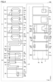
- FIG. 4 is an exploded plan view showing the configuration of the filter device 100 according to the first embodiment.
- the first conductor patterns 1a to 1d, the second conductor patterns 2a to 2d, the wiring patterns 11a to 11b, 21e, 51c, 52c, 52 to 56, and the electrode patterns 5a to 5c are each formed on the insulating substrates 3a to 3n by a printing method.
- the first conductor pattern 1a which constitutes part of the first inductor L1, is formed on the insulating substrate 3a.
- the first conductor pattern 1a is a hexagonal pattern that goes counterclockwise for approximately one revolution from the lower left side of the insulating substrate 3a in the figure.
- the starting end of the first conductor pattern 1a is electrically connected to the external electrode 4a (see FIG. 1) via the wiring pattern 11a.
- a connection portion 31a that connects to the via conductor 31 is provided near the end of the first conductor pattern 1a, and a connection portion 32a that connects to the via conductor 32 is provided midway along the first conductor pattern 1a.
- a first conductor pattern 1b constituting a part of the first inductor L1 is formed on the insulating substrate 3b.
- the first conductor pattern 1b is a hexagonal pattern that goes clockwise approximately once around the insulating substrate 3b from the lower right side in the figure.
- the starting end of the first conductor pattern 1b is electrically connected to the external electrode 4b (see FIG. 1) via the wiring pattern 11b.
- a connection portion 31b that connects to the via conductor 31 is provided near the end of the first conductor pattern 1b, and a connection portion 32b that connects to the via conductor 32 is provided midway along the first conductor pattern 1b.
- a first conductor pattern 1c constituting a part of the first inductor L1 is formed on the insulating substrate 3c.
- the first conductor pattern 1c has the same shape as the first conductor pattern 1a, and is a hexagonal pattern that goes around the insulating substrate 3c counterclockwise from the lower left side in the figure.
- the starting end of the first conductor pattern 1c is electrically connected to the external electrode 4a (see FIG. 1) via the wiring pattern 11c.
- a connection portion 31c that connects to the via conductor 31 is provided near the end of the first conductor pattern 1c, and a connection portion 32c that connects to the via conductor 32 is provided midway through the first conductor pattern 1c.
- a first conductor pattern 1d that constitutes part of the first inductor L1 is formed on the insulating substrate 3d.
- the first conductor pattern 1d has the same shape as the first conductor pattern 1b, and is a hexagonal pattern that makes approximately one full turn clockwise from the lower right side of the insulating substrate 3d in the figure.
- the starting end of the first conductor pattern 1d is electrically connected to the external electrode 4b (see FIG. 1) via the wiring pattern 11d.
- a connection portion 31d that connects to the via conductor 31 is provided near the end of the first conductor pattern 1d, and a connection portion 32d that connects to the via conductor 32 is provided midway along the first conductor pattern 1d.
- the first inductor L1 is configured such that the first conductor patterns 1a and 1c are connected in parallel, and the first conductor patterns 1b and 1d are connected in parallel, and the parallel-connected first conductor patterns 1a and 1c are connected in series to the parallel-connected first conductor patterns 1b and 1d, so that two coils of approximately one turn are connected in parallel.
- the second conductor pattern 2b which constitutes part of the second inductor L2, is formed on the insulating substrate 3f.
- the second conductor pattern 2b is formed in a U-shaped pattern that goes counterclockwise for about 3/4 of the way around from the lower left side of the insulating substrate 3f in the figure.
- a connection portion 33b that connects to the via conductor 33 is provided near the start end of the second conductor pattern 2b
- a connection portion 34a that connects to the via conductor 34 is provided near the end end of the second conductor pattern 2b
- a connection portion 35a that connects to the via conductor 35 is provided midway through the second conductor pattern 2b.
- a second conductor pattern 2c that constitutes part of the second inductor L2 is formed on the insulating substrate 3g.
- the second conductor pattern 2c is formed into a U-shaped pattern that goes counterclockwise for about 3/4 of the way around from the upper center of the insulating substrate 3g in the figure.
- a connection portion 35b that connects to the via conductor 35 is provided near the start end of the second conductor pattern 2c
- a connection portion 36a that connects to the via conductor 36 is provided near the end end of the second conductor pattern 2c
- a connection portion 34b that connects to the via conductor 34 is provided midway through the second conductor pattern 2c.
- a second conductor pattern 2d that constitutes part of the second inductor L2 is formed on the insulating substrate 3h.
- the second conductor pattern 2d is an I-shaped pattern that extends from the lower right side of the insulating substrate 3h in the figure to the upper side.
- a connection portion 36b that connects to the via conductor 36 is provided near the starting end of the second conductor pattern 2d, and a connection portion 37a that connects to the via conductor 37 is provided near the end of the second conductor pattern 2d.
- the second inductor L2 has a coil of about two turns, with the second conductor patterns 2a to 2d connected in series.
- the opening of the second inductor L2 has a rectangular shape
- the opening of the first inductor L1 has a hexagonal shape.
- the inductance of the second inductor L2 can be increased by effectively using the space in the insulator 3.
- the opening of the first inductor L1 into a hexagonal shape, the area of overlap with the opening of the second inductor L2 when viewed from the top side can be changed, and the coupling coefficient k can be adjusted.
- the inductance of the first inductor L1 can be reduced, thereby improving the pass characteristics of the filter device 100.
- the shape of the opening of the first inductor L1 is not limited to a hexagon, and may be any shape other than a rectangle, such as an octagon.
- An electrode pattern 5a (first electrode pattern) that constitutes one electrode of the capacitor C1 is formed on the insulating substrate 3i.
- the electrode pattern 5a is provided on the right side within the insulator 3 when viewed in a plan view from the top surface. In other words, the electrode pattern 5a is provided in a position that does not overlap as much as possible with the openings of the first inductor L1 and the second inductor L2.
- the electrode pattern 5a has a connection portion 37b that connects to the via conductor 37.
- An electrode pattern 5b is formed on the insulating substrate 3j. When viewed from above, the electrode pattern 5b is provided at a position that overlaps with the electrode pattern 5a. The electrode pattern 5b is not electrically connected to the external electrode 4b (see FIG. 1) and is a floating electrode of the capacitor C1.
- the insulating substrate 3k has an electrode pattern 5c that constitutes the other electrode of the capacitor C1.
- the electrode pattern 5c is provided at a position opposite to the electrode pattern 5b when viewed from the top surface side.
- the electrode pattern 5c is electrically connected to the external electrodes 4b (see FIG. 1) on the opposing side surfaces via the wiring pattern 51c.
- the electrode pattern 5c has a connection portion 39a that connects to the via conductor 39.
- the insulating substrate 3k has a wiring pattern 52 at a position on the left side within the insulator 3 when viewed from the top surface side.
- the wiring pattern 52 is electrically connected to the external electrodes 4a (see FIG. 1) on the opposing side surfaces via the wiring pattern 52c.
- the wiring pattern 52 also has a connection portion 38a that connects to the via conductor 38.
- Capacitor C1 is composed of electrode patterns 5a, 5b, and 5c. Insulating substrates 3l to 3n are further provided below capacitor C1. Insulating substrate 3l is provided with wiring pattern 53 having connection portion 38b connecting to via conductor 38, and wiring pattern 54 having connection portion 39b connecting to via conductor 39 and connection portion 41a connecting to via conductor 41. Insulating substrate 3m is provided with wiring pattern 55 having connection portion 38c connecting to via conductor 38, and wiring pattern 56 having connection portion 41b connecting to via conductor 41. Insulating substrate 3n is provided with connection portion 38d connecting to via conductor 38 and connection portion 41c connecting to via conductor 41. Via conductor 38 is electrically connected to external electrode 4a provided on the bottom surface via connection portion 38d, and via conductor 41 is electrically connected to external electrode 4b provided on the bottom surface via connection portion 41c.
- Fig. 5 is a perspective view of a filter device 200 according to the second embodiment.
- the short side direction of the filter device 200 is the X direction
- the long side direction is the Y direction
- the height direction is the Z direction.
- the same components as those in the filter device 100 shown in Fig. 1 are denoted by the same reference numerals, and detailed description will not be repeated.
- the filter device 200 is a rectangular parallelepiped chip component in which two inductors and one capacitor are stacked in the Z direction. As shown in FIG. 5, the filter device 200 is composed of an insulator 3 in which multiple insulating substrates (insulator layers) on which the first conductor pattern of the first inductor L1, the second conductor pattern of the second inductor L2, and the electrode pattern of the capacitor C1 are formed are stacked.
- the filter device 200 has the same configurations of the first inductor L1 and the capacitor C1 as the filter device 100 shown in FIG. 1, but the configuration of the second inductor L2 is different.
- the second inductor L2 has multiple second conductor patterns 2a-2d stacked parallel to the main surface of the insulator 3, with each of the second conductor patterns 2a-2d electrically connected by via conductors 33-36.
- the second conductor pattern 2a and the external electrode 4b are electrically connected to the side (first side) of the insulator 3 via the wiring pattern 22e.
- the second conductor pattern 2a and the external electrode 4a are not electrically connected.
- the path from the wiring patterns 11b, 11d provided at one end of the first inductor L1 through the external electrode 4b on the side (first side) of the insulator 3 to the wiring pattern 22e provided at one end of the second inductor L2 constitutes the third inductor L3. Since the third inductor L3 is formed only with the external electrode 4b provided on one side of the insulator 3, the inductance is smaller than when the inductor is formed with the external electrodes 4b provided on both sides of the insulator 3 as shown in FIG. 1. The opening surface of the third inductor L3 shown in FIG. 5 is also formed on the XZ plane. Therefore, the magnetic coupling between the first inductor L1 and the third inductor L3 is weaker than the magnetic coupling between the first inductor L1 and the second inductor L2.
- the second inductor L2, the third inductor L3, and the capacitor C1 are connected in series within the insulator 3 to form an LC series resonator. Therefore, the filter device 200 generates an attenuation pole by the LC series resonator and has a resonant frequency.
- Fig. 6 is an exploded plan view showing the configuration of a filter device 200 according to a second embodiment.
- the filter device 200 has the same configuration as the filter device 100 shown in Fig. 1 except for the configuration of the second inductor L2, so an exploded plan view of the capacitor C1 is omitted in Fig. 6, and the same components are denoted by the same reference numerals and detailed description will not be repeated.
- the second conductor pattern 2a which constitutes a part of the second inductor L2, is formed on the insulating substrate 3e.
- the second conductor pattern 2a is formed as an L-shaped pattern that goes clockwise from the lower right side of the insulating substrate 3e in the figure to about 1/2 a turn.
- the starting end of the second conductor pattern 2a is electrically connected to the external electrode 4b (see FIG. 5) via the wiring pattern 22e.
- a connection portion 33a that connects to the via conductor 33 is provided in the middle of the end of the second conductor pattern 2a.
- the second conductor pattern 2a and the second conductor pattern 2b flow in opposite directions, and the inductance value of the second inductor L2 is small.
- the second conductor pattern 2a it is also possible to connect the second conductor pattern 2a to the wiring pattern 22e from the left side in the figure, passing above, rather than in an L-shape.
- the current flows in the same direction in the second conductor pattern 2a and the second conductor pattern 2b, so the inductance value of the second inductor L2 is larger than the pattern in FIG. 5.
- the inductance value may be adjusted by adding a reverse pattern to the connection position.
- FIG. 7 is a graph showing the attenuation characteristics of the filter device 200 according to the second embodiment.
- the horizontal axis shows the frequency
- the vertical axis shows the attenuation characteristics, with the amount of attenuation increasing toward the bottom of the figure.
- the resonant frequency f0 of the filter device 100 is about 4.85 GHz
- the resonant frequency f0 of the filter device 200 is about 5.05 GHz. Therefore, it can be seen from FIG.
- the resonant frequency f0 of the filter device 200 is higher due to the smaller inductance of the third inductor L3 compared to the filter device 100.
- the width of each attenuation pole shown in FIG. 7 is also approximately the same.
- the resonant frequency f0 of the filter device 200 is lower than the resonant frequency f0 of a filter device that does not have the third inductor L3.
- Fig. 8 is a perspective view of a filter device 300 according to the third embodiment.
- the short side direction of the filter device 300 is the X direction
- the long side direction is the Y direction
- the height direction is the Z direction.
- the same components as those in the filter device 100 shown in Fig. 1 are denoted by the same reference numerals, and detailed description will not be repeated.
- the filter device 300 is a rectangular parallelepiped chip component in which two inductors and one capacitor are stacked in the Z direction. As shown in FIG. 8, the filter device 300 is composed of an insulator 3 in which multiple insulating substrates (insulator layers) on which the first conductor pattern of the first inductor L1, the second conductor pattern of the second inductor L2, and the electrode pattern of the capacitor C1 are formed are stacked. In the filter device 300, the configurations of the first inductor L1 and the second inductor L2 are the same as those of the filter device 100 shown in FIG. 1, but the configuration of the capacitor C1 is different.
- multiple electrode patterns 5a to 5c are stacked on the lower layer of the second inductor L2 with an insulating layer interposed between them.
- the second conductor pattern 2d (see FIG. 4) of the second inductor L2 and the electrode pattern 5a are electrically connected by a via conductor 37.
- the electrode pattern 5b is not electrically connected to the external electrode 4b or other wiring patterns, and is a floating electrode.
- the electrode pattern 5c is electrically connected to the external electrode 4b on one side (first side) of the insulator 3 through the wiring pattern 51c.
- the electrode pattern 5c does not have a via conductor 41 that electrically connects to the external electrode 4b.
- the capacitor C1 has no path for flowing electricity from the external electrode 4b provided on one side (first side) to the external electrode 4b provided on the other side (second side) through the electrode pattern 5c and the wiring pattern 51c, nor has a path for flowing electricity from the external electrode 4b provided on one side to the external electrode 4b provided on the bottom surface through the via conductor 41.
- the path from the wiring patterns 11b and 11d at one end of the first inductor L1 through the external electrode 4b on the side (first side) of the insulator 3, the external electrode 4b on the bottom, and the external electrode 4b on the side (second side) to the wiring pattern 21e at one end of the second inductor L2 constitutes the third inductor L3.
- the third inductor L3 does not pass inside the insulator 3, but forms an inductor through the external electrode 4b provided on the outside of the insulator 3, so that the inductance is larger than when the inductor is formed through a path that passes inside the insulator 3 as shown in FIG. 1.
- the opening surface of the third inductor L3 shown in FIG. 8 is also formed on the XZ plane. Therefore, the magnetic coupling between the first inductor L1 and the third inductor L3 is weaker than the magnetic coupling between the first inductor L1 and the second inductor L2.
- the second inductor L2, the third inductor L3, and the capacitor C1 are connected in series within the insulator 3 to form an LC series resonator. Therefore, the filter device 300 generates an attenuation pole by the LC series resonator and has a resonant frequency.
- Fig. 9 is an exploded plan view showing the configuration of a filter device 300 according to a third embodiment.
- the filter device 300 has the same configuration as the filter device 300 shown in Fig. 1 except for the configuration of the capacitor C1, so that the exploded plan view of the first inductor L1 and the second inductor L2 is omitted in Fig. 9, the same components are denoted by the same reference numerals, and detailed description will not be repeated.
- An electrode pattern 5c constituting the other electrode of the capacitor C1 is formed on the insulating substrate 3k.
- the electrode pattern 5c is provided at a position facing the electrode pattern 5b when viewed from the top surface side.
- the electrode pattern 5c is electrically connected to the external electrode 4b (see FIG. 8) on one side surface via the wiring pattern 51c. Therefore, the electrode pattern 5c is not electrically connected to the external electrode 4b (see FIG. 8) on the other side surface.
- the wiring pattern 51c is also extended to the external electrode 4b side of the other side surface that is not electrically connected, as shown in FIG. 9.
- the insulating substrate 3k is provided with a wiring pattern 52 at a position on the left side within the insulator 3 when viewed from the top surface side.
- the wiring pattern 52 is electrically connected to the external electrodes 4a on both opposing side surfaces via the wiring pattern 52c.
- the wiring pattern 52 also has a connection portion 38a that connects to the via conductor 38.
- Capacitor C1 is made up of electrode patterns 5a, 5b, and 5c. Insulating substrates 3l to 3n are further provided below capacitor C1. Insulating substrate 3l is provided with wiring pattern 53 having connection portion 38b that connects to via conductor 38. Insulating substrate 3m is provided with wiring pattern 55 having connection portion 38c that connects to via conductor 38. Insulating substrate 3n is provided with connection portion 38d that connects to via conductor 38. Via conductor 38 is electrically connected to external electrode 4a provided on the bottom surface through connection portion 38d. Note that filter device 300 does not have wiring patterns 54, 56 and via conductors 39, 41 provided in filter device 100 shown in FIG. 1.
- FIG. 10 is a graph showing the attenuation characteristics of the filter device 300 according to the third embodiment.
- the horizontal axis shows the frequency
- the vertical axis shows the attenuation characteristics, with the amount of attenuation increasing downward in the figure.
- the resonant frequency f0 of the filter device 100 is about 4.85 GHz
- the resonant frequency f0 of the filter device 300 is about 4.50 GHz. Therefore, it can be seen from FIG.
- the second path TL2 is described as a short path, but the second path TL2 can be regarded as a short path by making the inductance of the second path TL2 smaller than the mutual inductance M between the first inductor L1 and the second inductor L2. Therefore, it is preferable that the inductance of the second path TL2 is smaller than the mutual inductance M between the first inductor L1 and the second inductor L2.
- the first inductor L1 is electrically connected to the external electrode 4b via the first conductor patterns 1b and 1d
- the second inductor L2 is electrically connected to the external electrode 4b via the second conductor pattern 2a
- the conductor patterns electrically connected to the external electrode 4b are not limited to the first conductor patterns 1b and 1d and the second conductor pattern 2a, and may be other conductor patterns.
- the path constituting the third inductor L3 becomes longer. This increases the inductance.
- the position at which the first conductor patterns 1b, 1d and the external electrode 4b are electrically connected, and the position at which the second conductor pattern 2a and the external electrode 4b are electrically connected are not particularly limited, but the coupling coefficient k can be changed by moving the connection position in the Y-axis direction. For example, if the connection position is located closer to the center of the insulator 3, the area of the openings of the first inductor L1 and the second inductor L2 becomes smaller, and the coupling coefficient k can be reduced. On the other hand, if the connection position is located closer to the end of the insulator 3, the area of the openings of the first inductor L1 and the second inductor L2 becomes larger, and the coupling coefficient k can be increased.
- FIG. 11 is a circuit diagram of antenna devices 150a and 150b according to Modification 1. Note that in the antenna devices 150a and 150b shown in FIG. 11, the same components as those in the antenna device 150 shown in FIG. 2 are denoted by the same reference numerals, and detailed descriptions will not be repeated.
- the antenna device 150a shown in FIG. 11(a) includes a power feed circuit RF1, a filter device 100, a matching circuit 110, and a radiating element 155.
- the radiating element 155 and the power feed circuit RF1 are connected by a wiring 101, and the filter device 100 and the matching circuit 110 are connected in series to the wiring 101.
- the matching circuit 110 is provided between the power feed circuit RF1 and the filter device 100.
- the matching circuit 110 is a circuit for matching impedance with the radiating element 155, the power feed circuit RF1, the filter device 100, etc., and is composed of a resistor, an inductor, a capacitor, etc.
- the matching circuit may be provided not only between the feed circuit RF1 and the filter device 100, but also between the filter device 100 and the radiating element 155.
- the antenna device 150b shown in FIG. 11(b) includes the feed circuit RF1, the filter device 100, matching circuits 110 and 120, and the radiating element 155.
- the antenna device 150b further includes a matching circuit 120 between the filter device 100 and the radiating element 155.
- the matching circuit 120 is connected in series to the wiring 101, and is a circuit for matching impedance with the radiating element 155, the feed circuit RF1, the filter device 100, etc.
- the matching circuit 120 is composed of resistance, inductance, capacitance, etc., and may be a circuit of the same configuration as the matching circuit 110 or a circuit of a different configuration.
- the matching circuit 110 is provided between the power supply circuit RF1 and the filter device 100, and the matching circuit 120 is provided between the filter device 100 and the radiating element 155, but the configuration may include only the matching circuit 120. Furthermore, in the antenna device 150a shown in FIG. 11(a) and the antenna device 150b shown in FIG. 11(b), the matching circuits 110 and 120 are connected in series to the wiring 101, but at least one of the matching circuits 110 and 120 may be connected in parallel (shunt connected) between the wiring 101 and ground (GND).
- FIG. 12 is a circuit diagram of antenna devices 150c and 150d according to the second modification. Note that in the antenna devices 150c and 150d shown in FIG. 12, the same components as those in the antenna device 150 shown in FIG. 2 are denoted by the same reference numerals, and detailed description will not be repeated.
- the antenna device 150c shown in FIG. 12(a) includes a power feed circuit RF1, a filter device 100, and a radiating element 155.
- the radiating element 155 and the power feed circuit RF1 are connected by a wiring 101, and the filter device 100 is connected in parallel between the wiring 101 and ground (GND).
- the antenna device 150c includes a filter device 100 in which a terminal P1 (first terminal) is connected to ground (GND) and a terminal P2 (second terminal) is connected to the wiring 101.
- the antenna device 150c nothing is connected to the wiring 102 to which the filter device 100 is connected, but a matching circuit may be connected.
- the antenna device 150d shown in FIG. 12(b) includes a power feed circuit RF1, the filter device 100, matching circuits 110 and 120, and a radiating element 155.
- the matching circuits 110 and 120 are connected in series to the wiring 102 to which the filter device 100 is connected.
- the matching circuit 110 is connected between the ground (GND) and the filter device 100, and the matching circuit 120 is connected between the filter device 100 and the wiring 101.
- the matching circuits 110 and 120 are circuits for matching impedance with the radiating element 155, the power supply circuit RF1, the filter device 100, etc.
- the matching circuits 110 and 120 are composed of resistors, inductances, capacitances, etc., but the matching circuits 110 and 120 may be circuits of the same configuration or circuits of different configurations.
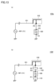
- FIG. 13 is a circuit diagram of antenna devices 150e and 150f according to modification example 3. Note that in the antenna devices 150e and 150f shown in FIG. 13, the same components as those in the antenna device 150 shown in FIG. 2 are denoted by the same reference numerals, and detailed description will not be repeated.
- the antenna device 150e shown in FIG. 13(a) includes a power feed circuit RF1, a filter device 100, and a radiating element 155.
- the radiating element 155 is, for example, an inverted-F antenna, and has a short-circuit point P3.
- the short-circuit point P3 is connected to ground (GND) via a wiring 103.
- the filter device 100 is not provided on the wiring 101 that connects the radiating element 155 and the power feed circuit RF1, but on the wiring 103.
- the antenna device 150e includes a filter device 100 that is connected in parallel to the power feed circuit RF1.
- the antenna device 150e includes a filter device 100 whose terminal P1 (first terminal) is connected to ground (GND) and whose terminal P2 (second terminal) is connected to the short-circuit point P3.
- the antenna device 150e nothing is connected to the wiring 103 to which the filter device 100 is connected, but a matching circuit may be connected.
- the antenna device 150f shown in FIG. 13(b) includes a power supply circuit RF1, the filter device 100, matching circuits 110 and 120, and a radiating element 155.
- the matching circuits 110 and 120 are connected in series to the wiring 103 to which the filter device 100 is connected.
- the matching circuit 110 is connected between the ground (GND) and the filter device 100, and the matching circuit 120 is connected between the filter device 100 and the short-circuit point P3 of the radiating element 155.
- the matching circuits 110 and 120 are circuits for matching impedance with the radiating element 155, the power supply circuit RF1, the filter device 100, etc.
- the matching circuits 110 and 120 are composed of resistors, inductances, capacitances, etc., but the matching circuits 110 and 120 may be circuits of the same configuration or circuits of different configurations.
- a filter device is a filter device having an attenuation band, A first terminal; A second terminal; a first inductor connected to the first terminal; a series resonator disposed in the first path of a first path and a second path provided in parallel between the first inductor and the second terminal;
- the series resonator includes: A second inductor; a capacitor connected in series with the second inductor; a third inductor connected in series with the second inductor and the capacitor;
- the magnetic coupling between the first inductor and the third inductor is weaker than the magnetic coupling between the first inductor and the second inductor.
- the filter device according to the present disclosure can realize a steep filter device with an attenuation pole in the low frequency band by providing a third inductor with weak magnetic coupling.
- the inductance of the second path is smaller than the mutual inductance between the first inductor and the second inductor.
- the inductance of the first inductor is smaller than the combined inductance of the second inductor and the third inductor.
- the first inductor, the second inductor, the third inductor, and the capacitor are provided in an insulator having a pair of main surfaces facing each other and four side surfaces connecting the main surfaces;
- the insulator is A first external electrode constituting the first terminal; a second external electrode constituting the second terminal;
- the third inductor is provided by utilizing a portion of the second external electrode.
- an opening surface of the third inductor forming a coil is disposed perpendicular to an opening surface of the first inductor forming a coil.
- the second external electrode is provided on at least a first side surface and a second side surface opposite to the first side surface, one end of the first inductor is electrically connected to the second external electrode provided on the first side surface, one end of the second inductor is electrically connected to the second external electrode provided on the second side surface, and the other end of the second inductor is electrically connected to the first electrode of the capacitor; a second electrode of the capacitor facing the first electrode and electrically connected to the first side and the second side of the second external electrode;
- the third inductor is formed from a path extending from one end of the first inductor through the second external electrode on the first side surface, the second electrode of the capacitor, and the second external electrode on the second side surface to one end of the second inductor.
- the third inductor has a single path.
- the second external electrode is provided at least on a first side surface, a second side surface opposite to the first side surface, and a first main surface which is one of the main surfaces; one end of the first inductor is electrically connected to the second external electrode provided on the first side surface, one end of the second inductor is electrically connected to the second external electrode provided on the first side surface,
- the third inductor is formed of a path extending from one end of the first inductor through the second external electrode on the first side surface to one end of the second inductor.
- the second external electrode is provided at least on a first side surface, a second side surface opposite to the first side surface, and a first main surface which is one of the main surfaces; one end of the first inductor is electrically connected to the second external electrode provided on the first side surface, one end of the second inductor is electrically connected to the second external electrode provided on the second side surface,
- the third inductor is formed from a path extending from one end of the first inductor through the second external electrode on the first side surface, the second external electrode on the first main surface, and the second external electrode on the second side surface to one end of the second inductor.
- An antenna device is an antenna device capable of radiating radio waves, A radiating element; A feeding circuit for feeding a high frequency signal to the radiating element; An antenna device comprising: a filter device according to any one of claims 1 to 9, which is connected in series between a radiating element and a feeder circuit.
- An antenna device is an antenna device capable of radiating radio waves, A radiating element; A feeding circuit for feeding a high frequency signal to the radiating element;
- An antenna device comprising: a filter device according to any one of claims (1) to (9), the filter device including a first terminal connected to a ground and a second terminal connected to a wiring connecting a power supply circuit and a radiating element, or to a short point of the radiating element.
- 1a-1d first conductor pattern
- 2a-2d second conductor pattern
- 3 insulator
- 3a-3n insulating substrate
- 4a, 4b external electrodes
- 5a-5c electrode patterns
- 150, 150a-150f antenna device
- 155 radiating element
- L1 first inductor
- L2 second inductor
- L3 third inductor
- RF1 power supply circuit
- RS series resonator
- TL1 first path
- TL2 second path.
Landscapes
- Physics & Mathematics (AREA)
- Acoustics & Sound (AREA)
- Engineering & Computer Science (AREA)
- Power Engineering (AREA)
- Filters And Equalizers (AREA)
- Control Of Motors That Do Not Use Commutators (AREA)
Priority Applications (3)
| Application Number | Priority Date | Filing Date | Title |
|---|---|---|---|
| JP2025516523A JPWO2024224724A1 (https=) | 2023-04-28 | 2024-01-26 | |
| CN202480026753.1A CN121002773A (zh) | 2023-04-28 | 2024-01-26 | 滤波器装置和天线装置 |
| US19/351,353 US20260039268A1 (en) | 2023-04-28 | 2025-10-07 | Filter device and antenna device |
Applications Claiming Priority (2)
| Application Number | Priority Date | Filing Date | Title |
|---|---|---|---|
| JP2023-074456 | 2023-04-28 | ||
| JP2023074456 | 2023-04-28 |
Related Child Applications (1)
| Application Number | Title | Priority Date | Filing Date |
|---|---|---|---|
| US19/351,353 Continuation US20260039268A1 (en) | 2023-04-28 | 2025-10-07 | Filter device and antenna device |
Publications (1)
| Publication Number | Publication Date |
|---|---|
| WO2024224724A1 true WO2024224724A1 (ja) | 2024-10-31 |
Family
ID=93255840
Family Applications (1)
| Application Number | Title | Priority Date | Filing Date |
|---|---|---|---|
| PCT/JP2024/002365 Ceased WO2024224724A1 (ja) | 2023-04-28 | 2024-01-26 | フィルタ装置、およびアンテナ装置 |
Country Status (4)
| Country | Link |
|---|---|
| US (1) | US20260039268A1 (https=) |
| JP (1) | JPWO2024224724A1 (https=) |
| CN (1) | CN121002773A (https=) |
| WO (1) | WO2024224724A1 (https=) |
Citations (4)
| Publication number | Priority date | Publication date | Assignee | Title |
|---|---|---|---|---|
| JPS61287310A (ja) * | 1985-06-13 | 1986-12-17 | Matsushita Electric Ind Co Ltd | Lcバンドパスフイルタ− |
| JPH02159109A (ja) * | 1988-12-12 | 1990-06-19 | Matsushita Electric Ind Co Ltd | Lcバンドパスフィルタ |
| WO2016125515A1 (ja) * | 2015-02-02 | 2016-08-11 | 株式会社村田製作所 | 可変フィルタ回路、高周波モジュール回路、および、通信装置 |
| WO2017199745A1 (ja) * | 2016-05-17 | 2017-11-23 | 株式会社村田製作所 | Lcフィルタ |
-
2024
- 2024-01-26 CN CN202480026753.1A patent/CN121002773A/zh active Pending
- 2024-01-26 JP JP2025516523A patent/JPWO2024224724A1/ja active Pending
- 2024-01-26 WO PCT/JP2024/002365 patent/WO2024224724A1/ja not_active Ceased
-
2025
- 2025-10-07 US US19/351,353 patent/US20260039268A1/en active Pending
Patent Citations (4)
| Publication number | Priority date | Publication date | Assignee | Title |
|---|---|---|---|---|
| JPS61287310A (ja) * | 1985-06-13 | 1986-12-17 | Matsushita Electric Ind Co Ltd | Lcバンドパスフイルタ− |
| JPH02159109A (ja) * | 1988-12-12 | 1990-06-19 | Matsushita Electric Ind Co Ltd | Lcバンドパスフィルタ |
| WO2016125515A1 (ja) * | 2015-02-02 | 2016-08-11 | 株式会社村田製作所 | 可変フィルタ回路、高周波モジュール回路、および、通信装置 |
| WO2017199745A1 (ja) * | 2016-05-17 | 2017-11-23 | 株式会社村田製作所 | Lcフィルタ |
Also Published As
| Publication number | Publication date |
|---|---|
| CN121002773A (zh) | 2025-11-21 |
| JPWO2024224724A1 (https=) | 2024-10-31 |
| US20260039268A1 (en) | 2026-02-05 |
Similar Documents
| Publication | Publication Date | Title |
|---|---|---|
| JP6801826B2 (ja) | フィルタ素子 | |
| US9203372B2 (en) | Common mode filter | |
| US10110196B2 (en) | Electronic component | |
| US8283990B2 (en) | Signal transmission communication unit and coupler | |
| US9225057B2 (en) | Antenna apparatus and wireless communication device using same | |
| US20130154783A1 (en) | High-frequency transformer, high-frequency component, and communication terminal device | |
| US11070187B2 (en) | Multilayer band pass filter | |
| US9013249B2 (en) | Electronic component | |
| US12094645B2 (en) | Antenna coupling element, antenna device, and communication terminal device | |
| CN211088515U (zh) | 天线耦合元件、天线装置及电子设备 | |
| JP5961813B2 (ja) | コモンモードノイズフィルタ | |
| US20230412137A1 (en) | Multilayer lc filter | |
| US20240235516A1 (en) | Filter device, antenna device, and antenna module | |
| JP5994108B2 (ja) | コモンモードノイズフィルタ | |
| US20250239780A1 (en) | Antenna device and electronic apparatus | |
| US11831292B2 (en) | LC composite component and communication terminal device | |
| WO2024224724A1 (ja) | フィルタ装置、およびアンテナ装置 | |
| CN117836880A (zh) | 线圈元件、天线装置及电子设备 | |
| KR20110094215A (ko) | 분포 정수 회로 | |
| JP7750313B2 (ja) | 電子部品 | |
| US20250309852A1 (en) | Filter device | |
| US20250239760A1 (en) | Antenna substrate and antenna module | |
| US20240030610A2 (en) | Monopole wire-patch antenna with enlarged bandwidth | |
| JP2005228857A (ja) | 高周波発振装置 |
Legal Events
| Date | Code | Title | Description |
|---|---|---|---|
| 121 | Ep: the epo has been informed by wipo that ep was designated in this application |
Ref document number: 24796483 Country of ref document: EP Kind code of ref document: A1 |
|
| WWE | Wipo information: entry into national phase |
Ref document number: 2025516523 Country of ref document: JP |
|
| NENP | Non-entry into the national phase |
Ref country code: DE |