WO2024224473A1 - 光ノードシステム、ノードおよび遠隔再起動方法 - Google Patents
光ノードシステム、ノードおよび遠隔再起動方法 Download PDFInfo
- Publication number
- WO2024224473A1 WO2024224473A1 PCT/JP2023/016245 JP2023016245W WO2024224473A1 WO 2024224473 A1 WO2024224473 A1 WO 2024224473A1 JP 2023016245 W JP2023016245 W JP 2023016245W WO 2024224473 A1 WO2024224473 A1 WO 2024224473A1
- Authority
- WO
- WIPO (PCT)
- Prior art keywords
- node
- light
- light source
- storage unit
- optical
- Prior art date
- Legal status (The legal status is an assumption and is not a legal conclusion. Google has not performed a legal analysis and makes no representation as to the accuracy of the status listed.)
- Ceased
Links
Images

Classifications
-
- H—ELECTRICITY
- H04—ELECTRIC COMMUNICATION TECHNIQUE
- H04B—TRANSMISSION
- H04B10/00—Transmission systems employing electromagnetic waves other than radio-waves, e.g. infrared, visible or ultraviolet light, or employing corpuscular radiation, e.g. quantum communication
-
- H—ELECTRICITY
- H04—ELECTRIC COMMUNICATION TECHNIQUE
- H04B—TRANSMISSION
- H04B10/00—Transmission systems employing electromagnetic waves other than radio-waves, e.g. infrared, visible or ultraviolet light, or employing corpuscular radiation, e.g. quantum communication
- H04B10/80—Optical aspects relating to the use of optical transmission for specific applications, not provided for in groups H04B10/03 - H04B10/70, e.g. optical power feeding or optical transmission through water
Definitions
- This disclosure relates to an optical node system, a node, and a remote restart method.
- optical line switching is performed at a certain frequency to connect optical fiber cores to optional routes and change routes in order to use the facilities efficiently during installation and maintenance.
- Non-Patent Document 1 Normally, such work requires a worker to go to the site and physically switch the connections, but a technology has been proposed that switches connections remotely using optical switches (Non-Patent Document 1). Also, a technology has been proposed that uses optical fiber power supply to drive optical nodes connected to optical fiber (Non-Patent Document 2).
- a parent node communicates optically with a child node, confirms completion of operations based on responses from the child node, and controls the child node.
- the control unit of the child node may fall into an infinite loop of abnormal processing, resulting in the parent node being unable to control the child node.
- one option would be to send a worker to the child node's location to repair the child node and restart the control unit, but repairs would take time and incur costs.
- This disclosure has been made in light of the above circumstances, and the purpose of this disclosure is to provide technology that allows child nodes to be restarted remotely without having to dispatch workers to the site.
- one aspect of the present disclosure is an optical node system including a first node and a second node, the first node including a first light source and a second light source that output light to the second node via an optical fiber, and a controller that instructs the discharge of a first storage unit of the second node, the second node including a remote drive unit that uses light from the first light source to store electricity in the first storage unit and is driven by electricity from the first storage unit, and a discharge unit that discharges the first storage unit using light from the second light source according to instructions from the controller, and the remote drive unit restarts after discharging the first storage unit.
- One aspect of the present disclosure is a node in an optical node system having multiple nodes, the node comprising: a remote drive unit that uses light output from other nodes to store electricity in a power storage unit and is driven by the electricity from the power storage unit; and a discharge unit that discharges the power storage unit using light different from the light output from the other nodes according to instructions from the other nodes, and the remote drive unit restarts after discharging the power storage unit.
- One aspect of the present disclosure is a remote restart method performed by an optical node system including a first node and a second node, the first node includes a first light source and a second light source that output light to the second node via an optical fiber, the first node supplies power to the second node using the light from the first light source, and if there is no response from the second node, instructs the second node to discharge a power storage unit using the light from the second light source, the second node stores power in the power storage unit using the light from the first light source, discharges the power storage unit using the light from the second light source according to the instruction from the first node, and restarts after the power storage unit is discharged.
- This disclosure provides a technology that allows child nodes to be restarted remotely without dispatching a worker to the site.
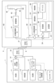
- FIG. 1 is a diagram showing the configuration of an optical node system according to the present embodiment.
- FIG. 2 is a flowchart showing the restart process of this embodiment.
- FIG. 1 shows the configuration of the optical node system of this embodiment.
- the optical node system of this embodiment includes a parent node 1 (first node) and a child node 2 (second node).
- the upstream parent node 1 and the downstream child node 2 are connected via an optical fiber 6 (optical fiber transmission path).
- optical fiber 6 optical fiber transmission path
- one child node 2 is connected to one optical fiber 6, but multiple child nodes 2 may be connected in series.
- parent node 1 and child node 2 are also referred to as optical nodes.
- Light is also referred to as an optical signal in the following description.
- the parent node 1 is installed in an environment where power is available (for example, in a communications building), supplies optical power (optical fiber power supply) to the child node 2, and communicates with the child node 2. Specifically, the parent node 1 outputs the power supply light of the light source A11 to the child node 2 via the optical fiber 6.
- the parent node 1 is equipped with the light source A11, a signal generating unit 12, a receiving unit 13, an optical circulator 14, and a controller 18 to supply optical power to the child node 2 and communicate with the child node 2.
- the optical circulator 14 splits the downstream optical signal (hereinafter, "downstream signal”) from the upstream optical signal (hereinafter, "upstream signal”).
- downstream signal and upstream signal are split through the optical circulator 14, and a single optical fiber 6 can connect the parent node 1 and the child node 2.
- the light source A11 outputs light (power supply light) to the child node 2 via the optical fiber 6.
- the light source A11 is, for example, a laser diode, and emits laser light.
- the laser light emitted from the light source A11 is input to the optical fiber 6 via the signal generation unit 12, the optical circulator 14, and the WDM coupler 19.
- the wavelength of the laser light is, for example, 1310 nm to 1659 nm.
- the power of the laser light is, for example, about +10 to 20 dBm.
- the light source A11 for power supply is used to transmit and receive upstream and downstream signals.
- the signal generating unit 12 modulates the light output from the light source A11 to generate a downstream signal (e.g., a control signal), superimposes the signal on the power supply light output from the light source A11, and outputs the signal to the child node 2.
- a downstream signal e.g., a control signal
- an external modulation method is used in which the light source A11 and the signal generation unit 12 are separate, but the light source A11 may be configured as an internal modulation type laser with the functions of the signal generation unit 12, and the downstream signal to the child node 2 may be superimposed on the power supply light.
- the receiver 13 receives the upstream signal output from the child node 2 via the optical fiber 6, converts it into an electrical signal, and outputs it to the controller 18.
- the upstream signal includes, for example, the response of the child node 2 to an instruction from the parent node 1, the amount of stored power in the power storage unit A33 measured by the child node 2, and the like.
- the receiver 13 uses a light receiving element such as a photodiode.
- the controller 18 controls the parent node 1 and the child node 2. For example, the controller 18 may instruct the child node 2 to discharge the power storage unit A33. Specifically, when there is no response from the second node, the controller 18 may instruct the child node 2 to discharge the power storage unit A33 using the light of the light source B15.
- the controller 18 sends a modulated signal to the signal generating unit 12 and superimposes a downstream signal (control signal) to the child node 2 on the power supply light output by the light source 11A.
- the downstream signal includes, for example, an instruction to drive the device 39, a power supply control instruction such as starting/stopping power supply, and an inquiry about the amount of stored power in the power storage unit A33.
- the controller 18 may also control the parent node 1 and the child node 2 based on the upstream signal output from the receiving unit 13, or may send the upstream signal to a management device (not shown).
- the parent node 1 forcibly discharges the power storage unit A33 by remote control when the child node 2 fails to respond (i.e., when the child node 2 is uncontrollable).
- the parent node 1 includes an optical pulse tester 16, a light source B15, a channel selector 17, and a WDM coupler 19.
- the optical pulse (test signal) of the optical pulse tester 16 and the light of the light source 11B are output to the child node 2 via the optical fiber 6.
- the optical pulse tester 16 generates optical pulses using a built-in light source (not shown) and tests the optical fiber 6. Specifically, the optical pulse tester 16 emits measurement optical pulses to the optical fiber 6 in response to instructions from the controller 18, and can detect losses due to bending, breakage, etc. of the optical fiber 6 from the reflected light. Note that the parent node 1 does not necessarily have to include the optical pulse tester 16.
- the controller 18 may drive the optical pulse tester 16, and if it determines based on the test results of the optical pulse tester 16 that there is no failure in the optical fiber 6, it may instruct the discharge of the power storage unit A33.
- Light source B15 emits light (laser light) in response to instructions from controller 18.
- the light from light source B15 is output to discharge unit 40 of child node 2 via channel selector 17, WDM coupler 19, and optical fiber 6.
- the wavelength of the light from light source B15 is different from that of light source A11.
- the optical node system includes multiple nodes 2, light (light source) with a different wavelength may be used for each child node 2.
- the channel selector 17 switches the path so that the light from the light source B15 or the optical pulse tester 16 is output to the optical fiber 6. Specifically, the channel selector 17 switches the path connecting to the WDM coupler 19 to the light source B15 or the optical pulse tester 16 in response to an instruction from the controller 18.
- WDM (Wavelength Division Multiplexing) couplers combine and demultiplex light of different wavelengths.
- the illustrated WDM coupler 19 (first coupler) multiplexes light of different wavelengths from light source A11 and light source B15 and outputs the multiplexed light to optical fiber 6.
- Child node 2 is installed in a location different from parent node 1.
- child node 2 may be installed in an outdoor manhole, on a utility pole, or in a communications building different from parent node 1.
- Child node 2 is connected to parent node 1 via optical fiber 6, and is a device capable of storing electricity through optical power supply. Therefore, child node 2 can be installed in a location without a power source.
- the child node 2 of this embodiment includes a WDM coupler 21, a remote drive unit 30, and a discharge unit 40.
- the WDM coupler 21 (second coupler) splits the wavelength of the light that has been wavelength-multiplexed by the WDM coupler 19, and outputs the light from the light source A11 to the remote drive unit 30 and outputs the light from the light source B15 to the discharge unit 40.
- the remote drive unit 30 stores electricity in the power storage unit A33 using the light from the light source A11, and is driven by the electricity from the power storage unit A33.
- the remote drive unit 30 also restarts after the discharge unit 40 discharges the power storage unit A33.
- the remote drive unit 30 receives the power supply light from the light source A11 of the parent node 1 at the photoelectric conversion unit A32 via the WDM coupler 21 and optical coupler 31, and stores it as electrical energy in the storage unit A33.
- the downstream signal superimposed on the power supply light from the light source A11 is input to the receiving unit 36 via the optical couplers 31, 35 and the optical circulator 34, where it is converted into an electrical signal and processed by the control unit 38.
- the light branched by the optical coupler 35 is input to the transmitting unit 37, where it is superimposed with the upstream signal and transmitted to the parent node 1.
- the remote drive unit 30 includes optical couplers 31 and 35 (power branching couplers), a photoelectric conversion unit A32, a power storage unit A33, an optical circulator 34, a receiving unit 36, a transmitting unit 37, a control unit 38, and a device 39.
- Optical coupler 31 splits the light output from parent node 1 via WDM coupler 21 into two.
- Optical coupler 31 is a multiplexer/demultiplexer that can multiplex/demultiplex downstream light and upstream light.
- Optical coupler 31 is a split ratio coupler that splits more of the downstream optical power output from parent node 1 to photoelectric conversion unit A32. The light with the smaller optical power split by optical coupler 31 is guided to optical circulator 34.
- the photoelectric conversion unit A32 converts one of the lights output from the optical coupler 31 into electrical energy and stores it in the storage unit A33.
- the photoelectric conversion unit A32 uses a photoelectric conversion element capable of receiving the wavelength of the laser light emitted by the light source A11.
- the power storage unit A33 stores the electrical energy converted by the photoelectric conversion unit A32.
- an electric double layer capacitor can be used for the power storage unit A33.
- the electrical energy stored in the power storage unit A33 serves as a power source for driving the remote control unit 30, such as the control unit 38 and the signal generation unit 12.
- Optical circulator 34 separates the other light branched off from optical coupler 31 into a downstream signal and an upstream signal.
- Optical coupler 35 branches the light separated by optical circulator 34. The light branched off by optical coupler 35 is guided to receiver 36, which receives it as a downstream signal, and transmitter 37, which generates an upstream signal.
- the receiver 36 receives one of the lights split by the optical coupler 35 as a downstream signal.
- the receiver 36 uses a light receiving element such as a photodiode.
- the transmitter 37 modulates the other light branched by the optical coupler 35 to generate modulated light, and outputs the modulated light to the parent node 1.
- the transmitter 37 has a reflective optical switch (not shown) that performs modulation synchronized with a signal from the controller 38, and uses the optical switch to modulate the light branched by the optical coupler 35 to generate modulated light.
- the modulated light is output to the parent node 1 via the optical fiber 6 as an upstream signal to the parent node 1. It is preferable that the transmitter 37 operates at a low voltage with little power consumption, and for example, a MEMS type ON/OFF switch using a mirror can be used.
- a laser light source may also be used for the transmitter 37.
- the control unit 38 is driven by the electrical energy of the power storage unit A33.
- the control unit 38 analyzes the downstream signal (control signal) received by the receiving unit 36, and executes instructions from the parent node 1.
- the instructions from the parent node 1 include various instructions such as an instruction to obtain the amount of stored power in the power storage unit A33, and an instruction to drive the device 39.
- the control unit 38 may be a microcomputer such as a PIC microcomputer.
- the control unit 38 controls active elements such as the transmitter 37 and device 39 according to instructions from the parent node 1. For example, the control unit 38 generates an upstream signal by modulating an optical switch provided in the transmitter 37.
- the upstream signal includes, for example, a response to an instruction from the parent node 1.
- the control unit 38 may also measure the voltage of the power storage unit A33 using an AD converter (not shown) or the like, generate an upstream signal including the measured voltage using the transmitter 37, and transmit it to the parent node 1.
- the device 39 uses the electrical energy of the power storage unit A33 to operate according to the instructions of the parent node 1 analyzed by the control unit 38.
- the device 39 can be, for example, a device with a core switching function, an optical element with a function for monitoring the connection state of the optical fiber 6, or an ICT device that can be operated with low power (for example, a sensor).
- the discharge unit 40 discharges the storage unit A33 using the light from the light source B15 according to instructions from the controller 18 of the parent node 1. Specifically, the discharge unit 40 converts the light energy input from the light source B15 into electrical energy using the photoelectric conversion unit B41, stores the electrical energy in the storage unit B42, and uses the electrical energy from the storage unit B42 to drive a transistor 44 (non-contact switch), thereby discharging the electrical energy stored in the storage unit A33. Note that if the transistor 44 can be driven without using the storage unit B42, the storage unit B42 can be omitted.
- the illustrated discharge unit 40 includes a photoelectric conversion unit B41, a light source B42, a resistor 43, a transistor 44, and a discharge adjustment load 45.
- the resistor 43, the transistor 44, and the discharge adjustment load 45 are also referred to as a reset switch circuit.
- the photoelectric conversion unit B41 converts the light of the light source B15 output via the WDM coupler 21 into electrical energy and stores it in the storage unit B42.
- the storage unit B42 stores the electrical energy converted from the light of the light source B15.
- the photoelectric conversion unit B41 drives the transistor 44 when a predetermined amount of electrical energy is stored in the storage unit B42. That is, the transistor 44 drives (ON) when the voltage of the storage unit B42 exceeds a predetermined value.
- the ON/OFF operation of the transistor 44 is controlled by the controller 18 starting/stopping the supply of light from the light source B15.
- the photoelectric conversion unit B41 applies a voltage to the transistor 44 via a resistor 43, and inputs a base current equal to or greater than the base-emitter voltage of the transistor 44.
- a collector current flows from the power storage unit A32 via the discharge adjustment load 45, and the electrical energy of the power storage unit A33 is discharged.
- the transistor 44 may be an npn junction bipolar transistor 44.
- the magnitude of the collector current can be arbitrarily designed for the capacitance and storage voltage of the storage unit A33 and the specifications of the transistor 44.
- the discharge time of the power storage unit A33 can be controlled by controlling the time of optical power supply from the light source B15 with the controller 18. For example, if the capacity of the power storage unit A33 and the upper limit of the storage voltage are determined at the time of system design, the magnitude of the collector current can be adjusted to control the discharge time. For example, if the power storage unit A33 is composed of a capacitor, and the capacitor is 2.5F and 3V, using a resistor of 100R for the discharge adjustment load 45 allows the capacitor to be discharged to near 0V within 10 minutes.
- the discharge unit 40 of this embodiment can forcibly discharge the electrical energy of the power storage unit A33, and discharge the voltage of the power storage unit A33 to near 0V in a short period of time. This makes it possible to shut down (forcefully terminate) the control unit 38.
- a transistor 44 is used, but this is not limited to this, and a non-contact switch other than a transistor 44 may also be used.
- FIG. 2 is a flowchart showing an example of the restart process of this embodiment.
- the parent node 1 (controller 18) sends a downstream signal to the child node 2 via the optical fiber 6, instructing the child node 2 to execute a specified process.
- the parent node 1 then waits for a response (upstream signal) from the child node 2 regarding the instruction (S11). If a response is received from the child node 2 within a specified time (S12: YES), the parent node 1 determines that the child node 2 is operating normally, returns to S11, and sends the next instruction to the child node 2.
- the parent node 1 drives the optical pulse tester 16 to perform an optical pulse test (S13). If the optical pulse tester 16 is not connected to the WDM coupler 19, the parent node 1 switches the channel selector 17 to connect the path of the optical pulse tester 16 to the WDM coupler 19.
- the parent node 1 uses the test results of the optical pulse tester 16 to determine whether or not there is a failure in the optical fiber 6 (S14). If there is a failure in the optical fiber 6 (S14: YES), the parent node 1 outputs an error message including the test results to an administrator terminal (not shown) or the like, and notifies the request for the dispatch of a worker (S20). The operator of the optical node system sees the error message on the administrator terminal and arranges for a worker to repair the failure in the optical fiber 6 on-site.
- the parent node 1 forcibly discharges the power storage unit A33 of the child node 2. Specifically, the parent node 1 starts optical power supply from the light source B15 to the discharge unit 40 (S15). At this time, the parent node 1 switches the channel selector 17 to connect the path of the light source B15 to the WDM coupler 19.
- the power supply light from the light source B15 is output to the discharge unit 40, and the electrical energy converted from the power supply light is stored in the power storage unit B42.
- the transistor 44 is driven (ON), and a collector current flows from the power storage unit A32 via the discharge adjustment load 45, forcibly discharging the power storage unit A33 (S16).
- the control unit 38 is shut down, and the control unit 38 can be reset.
- parent node 1 stops light source B15 and ends the optical power supply to power storage unit B42 (S17).
- power storage unit B42 S17
- electrical energy is recharged in power storage unit A33 by the light supplied by light source A11.
- control unit 38 restarts autonomously (S18). That is, when the voltage of power storage unit A33 rises to a value required for startup of control unit 38 and is recharged, control unit 38 restarts. Control unit 38 is reset by the shutdown, so it restarts normally.
- the parent node 1 When a predetermined time has elapsed since the end of optical power supply to the light source B15 in S17 (S119: YES), the parent node 1 returns to S11 and transmits an instruction to the child node 2.
- the predetermined time is the time until the amount of stored power in the power storage unit A33 reaches the amount required to start the control unit 38, and is set in advance.
- parent node 1 may or may not stop light source A11. Even if electrical energy is continuously supplied to power storage unit A33 without stopping light source A11, it is possible to discharge power storage unit A33 to near 0V by appropriately designing discharge adjustment load 45. Furthermore, while power is being supplied from light source B15 to discharge unit 40, parent node 1 may stop light source A11 and temporarily stop the storage of power in power storage unit A33, and after power supply from light source B15 has ended, start light source A11 and resume the storage of power in power storage unit A33.
- the optical node system of this embodiment described above comprises a parent node 1 and a child node 2.
- the parent node 1 comprises a light source A11 and a light source B15 which output light to the child node 2 via an optical fiber 6, and a controller 18 which instructs the discharge of the power storage unit A33 of the child node 2.
- the child node 2 comprises a remote drive unit 30 which stores electricity in the power storage unit A33 using the light from the light source A11 and is driven by the electricity from the power storage unit A33, and a discharge unit 40 which discharges the power storage unit A33 using the light from the light source B15 according to the instructions of the controller 18.
- the remote drive unit 30 restarts after the power storage unit A33 is discharged.
- parent node 1 is equipped with light source A11 and light source B15 which output light to child node 2 via optical fiber 6, powers child node 2 using the light of light source A11, and if there is no response from child node 2, instructs child node 2 to discharge power storage unit A33 using the light of light source B15, and child node 2 stores power in power storage unit A33 using the light of light source A11, discharges power storage unit A33 using the light of light source B15 in accordance with the instruction of parent node 1, and restarts after power storage unit A33 has been discharged.
- the power supply light of the light source B15 which is separate from the main light source A11, is transmitted to the child node 2
- the power supply light of the light source B15 is used as a power source to drive the discharge unit 40
- the power supply from the power storage unit A33 of the child node 2 to the control unit 38 is forcibly discharged, and then the control unit 38 is restarted. This allows the control unit 38 to return from the fraudulent processing loop.
- the child node can be restarted remotely in a short time without dispatching a worker to the site.
- the parent node 1 detects a poor response from the child node 2
- the failure of the child node 2 can be restored in a short time and at low cost.
- a light source B15 for discharging is provided in addition to the light source A11 that is used during normal operation. This allows the parent node 1 to control the operation timing of the discharge unit 40 of the child node 2, and to restart and reset the child node 2 at the necessary timing, such as when the child node 2 has a poor response.
- the discharge unit 40 is driven using the power supply light of the light source B15 as a power source to restart the child node 2. Therefore, in this embodiment, the child node 2 can be restarted remotely in a short time without increasing the power consumption of the child node 2 under normal circumstances.
- the power supply light of the light source B15 which is separate from the light source A11, is used as the power source for the discharge unit 40, the power storage unit A33 can be discharged in a short time and the control unit 38 can be restarted without increasing the power consumption of the child node 2 under normal circumstances due to the light source A11.
- the controller 18 of the parent node 1 and the control unit 38 of the child node 2 in the embodiment described above can be, for example, a general-purpose computer system.
- the computer system includes a CPU (Central Processing Unit, processor), a memory, a storage (HDD: Hard Disk Drive, SSD: Solid State Drive), a communication device, an input device, and an output device.
- the memory and storage are storage devices.
- the functions of the controller 18 or the control unit 38 are realized by the CPU executing a predetermined program loaded onto the memory.
- the program of the controller 18 or the control unit 38 can be stored in a computer-readable recording medium such as an HDD, SSD, USB (Universal Serial Bus) memory, CD (Compact Disc), or DVD (Digital Versatile Disc), or can be distributed via a network.
- a computer-readable recording medium such as an HDD, SSD, USB (Universal Serial Bus) memory, CD (Compact Disc), or DVD (Digital Versatile Disc), or can be distributed via a network.
- the computer-readable recording medium is, for example, a non-transitory recording medium.
- the parent node 1 shown in FIG. 1 includes an optical pulse tester 16 and performs an optical pulse test before driving the discharge unit 40 of the child node 2.
- the parent node 1 may not include an optical pulse tester 16 and may drive the discharge unit 40 without performing an optical pulse test.
- the process proceeds to S15, and optical power supply from light source B15 is immediately started. If the parent node 1 does not include an optical pulse tester 16, the channel selector 17 is also unnecessary.
Landscapes
- Physics & Mathematics (AREA)
- Electromagnetism (AREA)
- Engineering & Computer Science (AREA)
- Computer Networks & Wireless Communication (AREA)
- Signal Processing (AREA)
- Optical Communication System (AREA)
Priority Applications (2)
| Application Number | Priority Date | Filing Date | Title |
|---|---|---|---|
| PCT/JP2023/016245 WO2024224473A1 (ja) | 2023-04-25 | 2023-04-25 | 光ノードシステム、ノードおよび遠隔再起動方法 |
| JP2025516346A JPWO2024224473A1 (https=) | 2023-04-25 | 2023-04-25 |
Applications Claiming Priority (1)
| Application Number | Priority Date | Filing Date | Title |
|---|---|---|---|
| PCT/JP2023/016245 WO2024224473A1 (ja) | 2023-04-25 | 2023-04-25 | 光ノードシステム、ノードおよび遠隔再起動方法 |
Publications (1)
| Publication Number | Publication Date |
|---|---|
| WO2024224473A1 true WO2024224473A1 (ja) | 2024-10-31 |
Family
ID=93256066
Family Applications (1)
| Application Number | Title | Priority Date | Filing Date |
|---|---|---|---|
| PCT/JP2023/016245 Ceased WO2024224473A1 (ja) | 2023-04-25 | 2023-04-25 | 光ノードシステム、ノードおよび遠隔再起動方法 |
Country Status (2)
| Country | Link |
|---|---|
| JP (1) | JPWO2024224473A1 (https=) |
| WO (1) | WO2024224473A1 (https=) |
Citations (3)
| Publication number | Priority date | Publication date | Assignee | Title |
|---|---|---|---|---|
| JP2011090590A (ja) * | 2009-10-24 | 2011-05-06 | Tokyo Univ Of Agriculture & Technology | センシングシステム |
| EP2493209A1 (en) * | 2011-02-28 | 2012-08-29 | Alcatel Lucent | Method of remote optical powering and communication in an optical communication network |
| WO2022130483A1 (ja) * | 2020-12-15 | 2022-06-23 | 日本電信電話株式会社 | 光給電システム、光給電方法及び受電光通信装置 |
-
2023
- 2023-04-25 WO PCT/JP2023/016245 patent/WO2024224473A1/ja not_active Ceased
- 2023-04-25 JP JP2025516346A patent/JPWO2024224473A1/ja active Pending
Patent Citations (3)
| Publication number | Priority date | Publication date | Assignee | Title |
|---|---|---|---|---|
| JP2011090590A (ja) * | 2009-10-24 | 2011-05-06 | Tokyo Univ Of Agriculture & Technology | センシングシステム |
| EP2493209A1 (en) * | 2011-02-28 | 2012-08-29 | Alcatel Lucent | Method of remote optical powering and communication in an optical communication network |
| WO2022130483A1 (ja) * | 2020-12-15 | 2022-06-23 | 日本電信電話株式会社 | 光給電システム、光給電方法及び受電光通信装置 |
Also Published As
| Publication number | Publication date |
|---|---|
| JPWO2024224473A1 (https=) | 2024-10-31 |
Similar Documents
| Publication | Publication Date | Title |
|---|---|---|
| US20120288273A1 (en) | Intelligent splitter monitor | |
| JP7533623B2 (ja) | 監視制御装置及び光給電システム | |
| US8478089B2 (en) | Optical switch and optical-switch control method | |
| US20090245786A1 (en) | Optical communication system, method of measuring optical transmission line in the optical communication system, transmitting station, and receiving station | |
| US20240280758A1 (en) | Optical node, rotation angle deviation compensation system and rotation angle deviation compensation method | |
| US12316385B2 (en) | Optical power supply system, wakeup method and optical communication device on the receiving side | |
| WO2024224473A1 (ja) | 光ノードシステム、ノードおよび遠隔再起動方法 | |
| JP7637388B2 (ja) | 光ファイバ経路切替装置及び方法 | |
| JP5070597B2 (ja) | 光伝送システム、光伝送方法、光スイッチ装置、センター装置、光カプラ装置、加入者装置及び光通信システム | |
| JP5632989B2 (ja) | センシング方法およびセンシングシステム | |
| Hehmann et al. | Remotely powered intelligent splitter monitor for fiber access networks | |
| JP5914405B2 (ja) | 光回線装置用の遠隔電源再起動装置 | |
| WO2012051829A1 (zh) | 光传送网络中远端失效设备的处理方法及系统 | |
| WO2025134198A1 (ja) | 光ノードシステム、ノード、制御装置、切替方法およびプログラム | |
| EP1486014B1 (en) | Optically powered and controlled optical switch | |
| CN109982171B (zh) | 一种可拉远多跳光接入网及智能管理系统 | |
| JP2006196938A (ja) | 光ネットワークシステム | |
| JP7740541B2 (ja) | 光通信システム、光ノード、および光給電方法 | |
| WO2024166300A1 (ja) | 光ノードシステム、給電制御方法、及びプログラム | |
| WO2024127592A1 (ja) | 浸水検知システム、浸水検知装置、及び浸水検知方法 | |
| US20250293769A1 (en) | Optical power supply system and failure location detection method | |
| WO2011116618A1 (zh) | 光网络单元异常发光故障隔离系统及方法 | |
| WO2024166191A1 (ja) | 光給電システム、光給電システムの復旧方法、及び、光ノード装置 | |
| JP7782689B2 (ja) | 光通信システム、光ノード、及び光給電方法 | |
| JP7761062B2 (ja) | 光ノード、遠隔制御システム、および遠隔制御方法 |
Legal Events
| Date | Code | Title | Description |
|---|---|---|---|
| 121 | Ep: the epo has been informed by wipo that ep was designated in this application |
Ref document number: 23935254 Country of ref document: EP Kind code of ref document: A1 |
|
| ENP | Entry into the national phase |
Ref document number: 2025516346 Country of ref document: JP Kind code of ref document: A |
|
| WWE | Wipo information: entry into national phase |
Ref document number: 2025516346 Country of ref document: JP |
|
| NENP | Non-entry into the national phase |
Ref country code: DE |
|
| 122 | Ep: pct application non-entry in european phase |
Ref document number: 23935254 Country of ref document: EP Kind code of ref document: A1 |