WO2024219030A1 - 積層セラミックコンデンサ - Google Patents
積層セラミックコンデンサ Download PDFInfo
- Publication number
- WO2024219030A1 WO2024219030A1 PCT/JP2024/001184 JP2024001184W WO2024219030A1 WO 2024219030 A1 WO2024219030 A1 WO 2024219030A1 JP 2024001184 W JP2024001184 W JP 2024001184W WO 2024219030 A1 WO2024219030 A1 WO 2024219030A1
- Authority
- WO
- WIPO (PCT)
- Prior art keywords
- electrode portion
- length
- principal surface
- layer
- laminate
- Prior art date
- Legal status (The legal status is an assumption and is not a legal conclusion. Google has not performed a legal analysis and makes no representation as to the accuracy of the status listed.)
- Ceased
Links
Images


Classifications
-
- H—ELECTRICITY
- H01—ELECTRIC ELEMENTS
- H01G—CAPACITORS; CAPACITORS, RECTIFIERS, DETECTORS, SWITCHING DEVICES, LIGHT-SENSITIVE OR TEMPERATURE-SENSITIVE DEVICES OF THE ELECTROLYTIC TYPE
- H01G4/00—Fixed capacitors; Processes of their manufacture
- H01G4/30—Stacked capacitors
-
- H—ELECTRICITY
- H01—ELECTRIC ELEMENTS
- H01G—CAPACITORS; CAPACITORS, RECTIFIERS, DETECTORS, SWITCHING DEVICES, LIGHT-SENSITIVE OR TEMPERATURE-SENSITIVE DEVICES OF THE ELECTROLYTIC TYPE
- H01G4/00—Fixed capacitors; Processes of their manufacture
- H01G4/002—Details
- H01G4/005—Electrodes
- H01G4/012—Form of non-self-supporting electrodes
-
- H—ELECTRICITY
- H01—ELECTRIC ELEMENTS
- H01G—CAPACITORS; CAPACITORS, RECTIFIERS, DETECTORS, SWITCHING DEVICES, LIGHT-SENSITIVE OR TEMPERATURE-SENSITIVE DEVICES OF THE ELECTROLYTIC TYPE
- H01G4/00—Fixed capacitors; Processes of their manufacture
- H01G4/002—Details
- H01G4/018—Dielectrics
- H01G4/06—Solid dielectrics
- H01G4/08—Inorganic dielectrics
- H01G4/12—Ceramic dielectrics
-
- H—ELECTRICITY
- H01—ELECTRIC ELEMENTS
- H01G—CAPACITORS; CAPACITORS, RECTIFIERS, DETECTORS, SWITCHING DEVICES, LIGHT-SENSITIVE OR TEMPERATURE-SENSITIVE DEVICES OF THE ELECTROLYTIC TYPE
- H01G4/00—Fixed capacitors; Processes of their manufacture
- H01G4/002—Details
- H01G4/228—Terminals
- H01G4/232—Terminals electrically connecting two or more layers of a stacked or rolled capacitor
Definitions
- This invention relates to multilayer ceramic capacitors.
- Patent Document 1 discloses a multilayer ceramic capacitor in which the dimension in the lamination direction of the ceramic layers is less than 0.3 mm. Furthermore, the multilayer ceramic capacitor described in Patent Document 1 has external electrodes that are composed of a base film made of a sintered metal film and a plating film placed on top of that.
- the main objective of this invention is to provide a multilayer ceramic capacitor that can prevent cracks from propagating from the tips of the external electrodes into the interior of the multilayer ceramic capacitor.
- the multilayer ceramic capacitor of the present invention comprises a laminate including a plurality of laminated ceramic layers, a first main surface and a second main surface facing each other in the lamination direction of the plurality of ceramic layers, a first side surface and a second side surface facing each other in a width direction perpendicular to the lamination direction, a first end surface and a second end surface facing each other in a length direction perpendicular to the lamination direction and the width direction, a first internal electrode layer alternately laminated with the plurality of ceramic layers and exposed at the first end surface, and a second internal electrode layer alternately laminated with the plurality of ceramic layers and exposed at the second end surface, a first external electrode covering a portion of the first main surface and at least a portion of the first end surface of the laminate, and a second external electrode covering a portion of the first main surface and at least a portion of the second end surface of the laminate,
- Each of the electrode and the second external electrode has a first main surface electrode portion arranged on the first main surface, a second main
- This invention makes it possible to disperse the locations where stress occurs and prevent cracks from propagating from the tips of the external electrodes into the interior of the multilayer ceramic capacitor.
- FIG. 1 is an external perspective view showing a multi-layer ceramic capacitor which is an example of a multi-layer ceramic capacitor according to a first embodiment of the present invention
- 1 is a front view showing a multi-layer ceramic capacitor which is an example of a multi-layer ceramic capacitor according to a first embodiment of the present invention
- 1 is a plan view showing a multi-layer ceramic capacitor which is an example of a multi-layer ceramic capacitor according to a first embodiment of the present invention
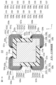
- FIG. 2 is a schematic cross-sectional view taken along line IV-IV in FIG.
- FIG. 2 is a schematic cross-sectional view taken along line VV in FIG.
- FIG. 6 is a schematic cross-sectional view taken along line VI-VI in FIG.
- FIG. 1 is a schematic cross-sectional view showing a multilayer ceramic capacitor as an example of a multilayer ceramic capacitor according to a modified example of the first embodiment of the present invention.
- FIG. 1 is a schematic cross-sectional view showing a multilayer ceramic capacitor as an example of a multilayer ceramic capacitor according to a modified example of the first embodiment of the present invention.
- FIG. 1 is a schematic cross-sectional view showing a multilayer ceramic capacitor as an example of a multilayer ceramic capacitor according to a modified example of the first embodiment of the present invention.
- FIG. 1 is a schematic cross-sectional view showing a multilayer ceramic capacitor as an example of a multilayer ceramic capacitor according to a modified example of the first embodiment of the present invention.
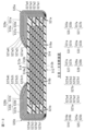
- FIG. 11 is an external perspective view showing a multi-layer ceramic capacitor which is an example of a multi-layer ceramic capacitor according to a second embodiment of the present invention.
- 12 is a schematic cross-sectional view taken along line XII-XII in FIG. 11, illustrating the structure of a multilayer ceramic capacitor which is an example of a multilayer ceramic capacitor according to a second embodiment of the present invention.
- FIG. 13 is a schematic cross-sectional view taken along line XIII-XIII in FIG. 11, illustrating the structure of a multilayer ceramic capacitor which is an example of a multilayer ceramic capacitor according to a second embodiment of the present invention.
- FIG. 14 is a schematic cross-sectional view taken along line XIV-XIV in FIG.
- FIG. 11 illustrating the structure of a multilayer ceramic capacitor which is an example of a multilayer ceramic capacitor according to a second embodiment of the present invention.
- FIG. 15 is a schematic cross-sectional view taken along line XV-XV in FIG. 11, illustrating the structure of a multilayer ceramic capacitor which is an example of a multilayer ceramic capacitor according to a second embodiment of the present invention.
- FIG. 16 is a schematic cross-sectional view taken along line XVI-XVI in FIG. 11, illustrating the structure of a multilayer ceramic capacitor which is an example of a multilayer ceramic capacitor according to a second embodiment of the present invention.
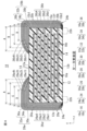
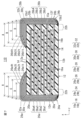
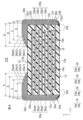
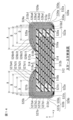
- FIG. FIG. 12 is an exploded perspective view of the laminate shown in FIG. 11 .
- FIG. 12 is an exploded perspective view of the laminate shown in FIG. 11 .
- FIG. 11 is an external perspective view showing a multi-layer ceramic capacitor which is an example of a multi-layer ceramic capacitor according to a third embodiment of the present invention.
- 15 is a schematic cross-sectional view taken along line XV-XV in FIG. 11, illustrating the structure of a multilayer ceramic capacitor which is an example of a multilayer ceramic capacitor according to a third embodiment of the present invention.
- FIG. FIG. 12 is a schematic cross-sectional view taken along line XX-XX in FIG. 11, illustrating the structure of a multilayer ceramic capacitor which is an example of a multilayer ceramic capacitor according to a third embodiment of the present invention.
- FIG. 1 is an external perspective view showing a multilayer ceramic capacitor as an example of a multilayer ceramic capacitor according to a first embodiment of the present invention.
- FIG. 2 is a front view showing a multilayer ceramic capacitor as an example of a multilayer ceramic capacitor according to a first embodiment of the present invention.
- FIG. 3 is a plan view showing a multilayer ceramic capacitor as an example of a multilayer ceramic capacitor according to a first embodiment of the present invention.
- FIG. 4 is a cross-sectional schematic diagram along line IV-IV in FIG. 1.
- FIG. 5 is a cross-sectional schematic diagram along line V-V in FIG. 1.
- FIG. 6 is a cross-sectional schematic diagram along line VI-VI in FIG. 1.
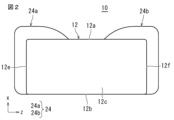
- the multilayer ceramic capacitor 10 has a laminate 12 and an external electrode 24. Below, the configuration of each component will be explained in the order of the laminate 12 and the external electrode 24.
- the laminate 12 has a plurality of laminated ceramic layers 14 and a plurality of internal electrode layers 16.
- the laminate 12 further includes a first main surface 12a and a second main surface 12b facing a height direction x, which is the lamination direction of the plurality of ceramic layers 14, a first side surface 12c and a second side surface 12d facing a width direction y perpendicular to the height direction x, and a first end surface 12e and a second end surface 12f facing a length direction z perpendicular to the height direction x and the width direction y.
- the corners and ridges of the laminate 12 are rounded. The corners are portions where three adjacent faces of the laminate 12 intersect, and the ridges are portions where two adjacent faces of the laminate 12 intersect. Furthermore, unevenness may be formed on part or all of the first main surface 12a and the second main surface 12b, the first side surface 12c and the second side surface 12d, and the first end surface 12e and the second end surface 12f.
- the laminate 12 has an effective layer portion 15a in which multiple internal electrode layers 16 face each other in the height direction x connecting the first main surface 12a and the second main surface 12b, a first outer layer portion 15b1 formed from multiple ceramic layers 14 located between the internal electrode layer 16 located closest to the first main surface 12a and the first main surface 12a, and a second outer layer portion 15b2 formed from multiple ceramic layers 14 located between the internal electrode layer 16 located closest to the second main surface 12b and the second main surface 12b.
- the first outer layer 15b1 is located on the first main surface 12a side of the laminate 12 and is an assembly of multiple ceramic layers 14 located between the first main surface 12a and the internal electrode layer 16 closest to the first main surface 12a.
- the second outer layer 15b2 is located on the second main surface 12b side of the laminate 12 and is an assembly of multiple ceramic layers 14 located between the second main surface 12b and the internal electrode layer 16 closest to the second main surface 12b.
- the area sandwiched between the first outer layer 15b1 and the second outer layer 15b2 is the effective layer 15a.
- the laminate 12 includes side portions 22a (W gaps) of the laminate 12 located between the effective layer portion 15a and the first side surface 12c and between the effective layer portion 15a and the second side surface 12d. Furthermore, the laminate 12 includes end portions 22b (L gaps) of the laminate 12 located between the effective layer portion 15a and the first end surface 12e and between the effective layer portion 15a and the second end surface 12f and including the lead-out electrode portion of either the first internal electrode layer 16a or the second internal electrode layer 16b described below.
- the number of ceramic layers 14 to be stacked is not particularly limited, but is preferably 3 to 1000, including the first outer layer 15b1 and the second outer layer 15b2.
- the thickness of the ceramic layer 14 is preferably 2.0 ⁇ m to 80 ⁇ m.
- the ceramic layer 14 may be formed of, for example, a dielectric material.
- a dielectric material for example, a dielectric ceramic composed of a main component such as BaTiO 3 , CaTiO 3 , SrTiO 3 , or CaZrO 3 may be used.
- a material containing a minor component such as a Mn compound, an Fe compound, a Cr compound, a Co compound, or a Ni compound in a smaller amount than the main component may be used.
- the ceramic layer 14 may have a plurality of crystal grains including a perovskite type compound having a basic structure of BaTiO 3 .
- the multiple inner ceramic layers 14 constituting the effective layer portion 15a are formed so as to be sandwiched between the first internal electrode layer 16a and the second internal electrode layer 16b of the multiple internal electrode layers 16.
- the inner ceramic layers 14 are composed of dielectric ceramic particles having a perovskite structure, with a perovskite-type compound containing Ba and Ti as the main component, for example. At least one of Si, Mg, Ba, and Mn may also be added as an additive to these main components. The additive is present between the ceramic particles.
- the first internal electrode layer 16a is disposed on the surface of the ceramic layer 14.
- the first internal electrode layer 16a has a first opposing electrode portion 18a that faces the second internal electrode layer 16b, and a first lead electrode portion 20a that is located on one end side of the first internal electrode layer 16a and extends from the first opposing electrode portion 18a to the first end face 12e of the laminate 12. The end of the first lead electrode portion 20a is led out to the first end face 12e and exposed.
- the shape of the second opposing electrode portion 18b of the second internal electrode layer 16b is not particularly limited, but is preferably rectangular in plan view. However, the corners in plan view may be rounded or may be formed at an angle in plan view (tapered). It may also be tapered in plan view, with a slope in either direction.
- the first internal electrode layer 16a and the second internal electrode layer 16b can be made of an appropriate conductive material, for example, metals such as Ni, Cu, Ag, Pd, Au, or alloys containing at least one of these metals, such as an Ag-Pd alloy, but are not limited to these.
- the first opposing electrode portion 18a of the first internal electrode layer 16a and the second opposing electrode portion 18b of the second internal electrode layer 16b face each other via the ceramic layer 14, forming a capacitance and exhibiting the characteristics of a capacitor.
- the external electrode 24 includes a base electrode layer 26 and a plating layer 28 formed to cover the base electrode layer 26.
- the second external electrode 24b is disposed on the second end face 12f of the laminate 12 and on a portion of the first main face 12a. In this case, the second external electrode 24b is electrically connected to the second extraction electrode portion 20b of the second internal electrode layer 16b.
- the second external electrode 24b may extend slightly around a portion of the first side face 12c and a portion of the second side face 12d.
- the first base electrode layer 26a is formed to cover a portion of the first main surface 12a on the side of the first end surface 12e of the laminate 12 and the first end surface 12e of the laminate 12.
- the second base electrode layer 26b is formed to cover a portion of the first main surface 12a on the second end surface 12f side of the laminate 12 and the second end surface 12f of the laminate 12.
- the first base electrode layer 26a and the second base electrode layer 26b each have a first main surface electrode portion, a second main surface electrode portion, a third main surface electrode portion, and a fourth main surface electrode portion.
- the first base electrode layer 26a has a configuration in which the first main surface electrode portion 26a1, the second main surface electrode portion 26a2, the third main surface electrode portion 26a3, and the fourth main surface electrode portion 26a4 are stacked.
- the second base electrode layer 26b has a configuration in which the first main surface electrode portion 26b1, the second main surface electrode portion 26b2, the third main surface electrode portion 26b3, and the fourth main surface electrode portion 26b4 are stacked.
- the first principal surface electrode portion 26a1 is arranged on the surface of the laminate 12
- the second principal surface electrode portion 26a2 is arranged on the surface of the first principal surface electrode portion 26a1
- the third principal surface electrode portion 26a3 is arranged on the surface of the second principal surface electrode portion 26a2
- the fourth principal surface electrode portion 26a4 is arranged on the surface of the third principal surface electrode portion 26a3.
- a direction is determined on the first main surface 12a that connects the end of the first main surface electrode portion of the first base electrode layer on the center side of the laminate to the surface where the first internal electrode layer is exposed on the surface of the laminate, specifically, a direction that connects the first end 26a1t of the first main surface electrode portion 26a1 of the first base electrode layer 26a on the center side of the laminate 12 to the first end surface 12e of the laminate 12 where the first lead electrode portion 20a of the first internal electrode layer 16a is exposed (hereinafter, the first reference direction).
- the first end 26a1t, second end 26a2t, third end 26a3t, and fourth end 26a4t of the first base electrode layer 26a on the central side of the laminate 12 are not aligned with each other, so that the stress of the external electrode 24 toward the central side of the laminate 12 that occurs during solder shrinkage can be dispersed.
- a direction connecting the end of the first main surface electrode portion of the second base electrode layer on the center side of the laminate to the surface where the second internal electrode layer is exposed on the surface of the laminate is determined, specifically, a direction connecting the first end 26b1t of the first main surface electrode portion 26b1 of the second base electrode layer 26b on the center side of the laminate 12 to the second end surface 12f of the laminate 12 where the second lead electrode portion 20b of the second internal electrode layer 16b is exposed (hereinafter, the second reference direction).
- the first principal surface electrode portion 26b1, the second principal surface electrode portion 26b2, the third principal surface electrode portion 26b3, and the fourth principal surface electrode portion 26b4 of the second base electrode layer 26b have first end 26b1t, second end 26b2t, third end 26b3t, and fourth end 26b4t on the central side of the laminate 12 that are not aligned with each other, so that the stress of the external electrode 24 toward the central side of the laminate 12 that occurs during solder shrinkage can be dispersed.
- the first end 26a1t of the first principal surface electrode portion 26a1 is not covered by the second principal surface electrode portion 26a2, the second end 26a2t of the second principal surface electrode portion 26a2 is not covered by the third principal surface electrode portion 26a3, and the third end 26a3t of the third principal surface electrode portion 26a3 is not covered by the fourth principal surface electrode portion 26a4.
- the stress acting on the first end 26a1t to the fourth end 26a4t of each of the first principal surface electrode portion 26a1 to the fourth principal surface electrode portion 26a4 can be concentrated toward the outside of the laminate 12 (the first end surface 12e side) rather than at these ends, dispersing the stress and improving the mechanical strength.
- first end 26b1t of the first principal surface electrode portion 26b1 is not covered by the second principal surface electrode portion 26b2
- the second end 26b2t of the second principal surface electrode portion 26b2 is not covered by the third principal surface electrode portion 26b3
- the third end 26b3t of the third principal surface electrode portion 26b3 is not covered by the fourth principal surface electrode portion 26b4.
- the stress acting on the first end 26b1t to the fourth end 26b4t of each of the first principal surface electrode portion 26b1 to the fourth principal surface electrode portion 26b4 can be concentrated toward the outside of the laminate 12 (the second end surface 12f side) rather than at these ends, dispersing the stress and improving the mechanical strength.
- each of the first to fourth main surface electrode portions constituting the base electrode layer 26 can be formed by a thin film formation method such as sputtering or vapor deposition, or by screen printing.
- each of the first to fourth principal surface electrode portions is formed by a thin film formation method, it can be made of a metal such as Cu, Cr, Au, Pt, Ag, Sn, Ti, or Ni.
- Each of the first to fourth principal surface electrode portions can be configured taking into consideration their respective functions.
- the first principal surface electrode portions 26a1 and 26b1 can be configured from NiCr or the like, taking into consideration adhesion to ceramics.
- the thickness of each of the first to fourth principal surface electrode portions in the direction connecting the first principal surface 12a and the second principal surface 12b of the laminate 12 is 10 ⁇ m or less. Therefore, the dimension of the laminated ceramic capacitor 10 in the lamination direction can be made sufficiently small, and the height can be reduced.
- each of the first to fourth principal surface electrode portions may be disposed on at least one of the first principal surface 12a or the second principal surface 12b of the laminate 12.
- the direct plating layer described below is not disposed on the second principal surface 12b, or, even if it is disposed on the second principal surface 12b, it is preferable that the amount of wraparound of the direct plating layer onto the first principal surface 12a is greater than the amount of wraparound of the direct plating layer onto the second principal surface 12b.
- each of the first to fourth principal surface electrode portions can be changed by changing the sputtering distance. For example, the thickness can be increased by shortening the ejection distance to the portion where the principal surface electrode portion is to be formed.
- each of the first to fourth principal surface electrode portions is formed by screen printing, it contains a ceramic component and a metal.
- the metal includes at least one of Cu, Ni, Ag, Pd, Ag-Pd alloy, and Au.
- each of the first principal surface electrode portions 26a1 and 26b1 may contain the same main component as the ceramic layer 14.
- each of the first principal surface electrode portions 26a1 and 26b1 preferably contains at least a portion of BaTiO 3. This can improve the adhesion between the laminate 12 and each of the first principal surface electrode portions 26a1 and 26b1.
- each of the first principal surface electrode portions 26a1 and 26b1 contains the same main component as the ceramic layer 14, the adhesion can be further improved by simultaneously firing the laminate 12 and each of the first principal surface electrode portions 26a1 and 26b1.
- the metal component is preferably Ni, Cu, etc., but can be changed as appropriate depending on the metal component of the internal electrode layer 16.
- the thickness of the portion of each of the first to fourth principal surface electrode portions that is disposed on the first principal surface 12a is preferably 0.5 ⁇ m or more and 3.0 ⁇ m or less.
- the plating layer 28 includes a first plating layer 28a and a second plating layer 28b.
- the first plating layer 28a is arranged to cover the first principal surface electrode portion 26a1 to the fourth principal surface electrode portion 26a4 as the first base electrode layer 26a.
- the second plating layer 28b is arranged to cover the first principal surface electrode portion 26b1 to the fourth principal surface electrode portion 26b4 as the second base electrode layer 26b.
- the plating layer 28 is formed of multiple layers. That is, the plating layer 28 has an underplating layer 30 and a top plating layer 32.
- the underplating layer 30 includes a first underplating layer 30a included in the first plating layer 28a and a second underplating layer 30b included in the second plating layer 28b.
- the top plating layer 32 includes a first top plating layer 32a included in the first plating layer 28a and a second top plating layer 32b included in the second plating layer 28b.
- the first underplating layer 30a of the underplating layer 30 is arranged to cover the fourth main surface electrode portion 26a4 of the first underelectrode layer 26a.
- the second underplating layer 30b of the underplating layer 30 is arranged to cover the fourth main surface electrode portion 26b4 of the second underelectrode layer 26b.
- the underplating layer 30 preferably contains at least one metal selected from, for example, Cu, Ni, Sn, Pb, Au, Ag, Pd, Bi, or Zn, or an alloy containing such a metal.
- the underplating layer 30 is preferably a Cu plating layer.
- the surface plating layer 32 may be formed of multiple layers.
- the surface plating layer 32 has a two-layer structure consisting of a middle plating layer 34, which is a Ni plating layer, and an upper plating layer 36, which is a Sn plating layer.
- the first intermediate plating layer 34a covers the first underplating layer 30a
- the first upper plating layer 36a covers the first intermediate plating layer 34a
- the second intermediate plating layer 34b covers the second underplating layer 30b
- the second upper plating layer 36b covers the second intermediate plating layer 34b.
- the middle plating layer 34 which is a Ni plating layer, can prevent the lower plating layer 30 from being eroded by solder when mounting the multilayer ceramic capacitor 10.
- the upper plating layer 36 which is a Sn plating layer, improves the wettability of the solder when mounting the multilayer ceramic capacitor 10, making mounting easier. If the plating layer 28 has a three-layer structure, in addition to the above, it is preferable that the layers are laminated in the order of a Sn plating layer, a Ni plating layer, and a Sn plating layer.
- the metal ratio per unit volume of the plating layer 28 is preferably 99% by volume or more.
- each plating layer of plating layer 28 is preferably 0.5 ⁇ m or more and 6.0 ⁇ m or less.
- the dimension in the length direction z of the multilayer ceramic capacitor 10 including the laminate 12, the first external electrode 24a, and the second external electrode 24b is defined as dimension L
- the dimension in the height direction x of the multilayer ceramic capacitor 10 including the laminate 12, the first external electrode 24a, and the second external electrode 24b is defined as dimension T
- the dimension in the width direction y of the multilayer ceramic capacitor 10 including the laminate 12, the first external electrode 24a, and the second external electrode 24b is defined as dimension W.
- the dimensions of the multilayer ceramic capacitor 10 are preferably such that the L dimension in the length direction z is 0.2 mm or more and 3.2 mm or less, the T dimension in the height direction x is 0.04 mm or more and 2.5 mm or less, and the W dimension in the width direction y is 0.1 mm or more and 2.5 mm or less.
- the first base electrode layer 26a is composed of a laminate of a first main surface electrode portion 26a1, a second main surface electrode portion 26a2, a third main surface electrode portion 26a3, and a fourth main surface electrode portion 26a4, and the second base electrode layer 26b is composed of a laminate of a first main surface electrode portion 26b1, a second main surface electrode portion 26b2, a third main surface electrode portion 26b3, and a fourth main surface electrode portion 26b4.
- the length of the first main surface electrode portion 26a1 in a first reference direction connecting the first end 26a1t on the center side of the laminate 12 of the first main surface electrode portion 26a1 of the first base electrode layer 26a to the first end surface 12e of the laminate 12 where the first lead electrode portion 20a of the first internal electrode layer 16a is exposed is length A
- the length of the second main surface electrode portion 26a2 in the same direction as length A is length B
- the length of the third main surface electrode portion 26a3 in the same direction as length A is length C
- the length of the fourth main surface electrode portion 26a4 in the same direction as length A is length D, so that length A > length B > length C > length D.
- the length of the first main surface electrode portion 26b1 in the second reference direction connecting the first end 26b1t on the center side of the laminate 12 of the first main surface electrode portion 26b1 of the second base electrode layer 26b to the second end surface 12f of the laminate 12 where the second lead electrode portion 20b of the second internal electrode layer 16b is exposed is length A
- the length of the second main surface electrode portion 26b2 in the same direction as length A is length B
- the length of the third main surface electrode portion 26b3 in the same direction as length A is length C
- the length of the fourth main surface electrode portion 26b4 in the same direction as length A is length D
- first end 26a1t, second end 26a2t, third end 26a3t, and fourth end 26a4t of the first main surface electrode portion 26a1 to the fourth main surface electrode portion 26a4 of the first base electrode layer 26a are not aligned with each other at the center of the laminate 12, and the first end 26b1t, second end 26b2t, third end 26b3t, and fourth end 26b4t of the first main surface electrode portion 26b1 to the fourth main surface electrode portion 26b4 of the second base electrode layer 26b are not aligned with each other at the center of the laminate 12, so that the stress of the external electrode 24 toward the center of the laminate 12 that occurs during solder shrinkage can be dispersed.
- the effect of this invention is more pronounced when the T dimension of the multilayer ceramic capacitor 10 is 150 ⁇ m or less. Furthermore, when the T dimension is 50 ⁇ m or less, the multilayer ceramic capacitor 10 is thin and more reliable mechanical strength is required, so the effect of this invention is more pronounced.
- the first principal surface electrode portion 26a1 to the fourth principal surface electrode portion 26a4 of the first base electrode layer 26a and the first principal surface electrode portion 26b1 to the fourth principal surface electrode portion 26b4 of the second base electrode layer 26b are each formed to extend around the first end face 12e and the second end face 12f, which are faces perpendicular to the first principal surface 12a.
- the locations (ridges, seams) where the first main surface 12a intersects with the first end surface 12e and the second end surface 12f are continuously covered with the first base electrode layer 26a and the second base electrode layer 26b, respectively, improving moisture resistance.
- first to fourth principal surface electrode portions 26a1 to 26a4 and the first to fourth principal surface electrode portions 26b1 to 26b4 of each of the external electrodes 24 are formed by a sputtering method.
- first external electrode 24a and the second external electrode 24b which are external electrodes 24 with a thickness of 10 ⁇ m or less, to be formed on each of the first end face 12e and the second end face 12f that are perpendicular to the first principal surface 12a, so that the dimensions of the multilayer ceramic capacitor 10 in the length direction z and width direction y can be reduced.
- the above lengths A, B, C and D of the first principal surface electrode portion 26a1 to the fourth principal surface electrode portion 26a4 of the first base electrode layer 26a and the first principal surface electrode portion 26b1 to the fourth principal surface electrode portion 26b4 of the second base electrode layer 26b can be measured by the following measurement method.
- the cross section is polished to 1/2 of the W dimension in the width direction y.
- the polished cross section is observed using a VHX. Note that if the first lead electrode portion 20a of the first internal electrode layer 16a or the second lead electrode portion 20b of the second internal electrode layer 16b is not present in the cross section, it is also possible to observe the main surface electrode portion directly above the first lead electrode portion 20a of the first internal electrode layer 16a or the second lead electrode portion 20b of the second internal electrode layer 16b by further polishing to 1/4 of the W dimension in the width direction y.
- first principal surface electrode portion 26a1 to the fourth principal surface electrode portion 26a4 and the first principal surface electrode portion 26b1 to the fourth principal surface electrode portion 26b4 of the second base electrode layer 26b are formed by a method such as sputtering, it is also possible to observe the differences in the components of each principal surface electrode portion using WDX or EDX using a TEM.
- the thickness of each layer of the principal surface electrode portion is about 1 ⁇ m, the composition of each layer can be confirmed by exposing a cross section (1/4LT cross section) of the central portion of the external electrode 24 and performing a composition analysis using WDX.
- the thickness of each layer of the principal surface electrode portion is 1 ⁇ m or less, the detailed structure can be confirmed by EDX using a TEM.
- the field of view is approximately 1 ⁇ m, and observations can be performed at a magnification of 20k.
- each of the lengths A, B, C, and D is defined by the straight-line distance between a perpendicular line drawn from the exposed portion of the lead electrode portion closest to the first main surface 12a, of the first lead electrode portion 20a of the first internal electrode layer 16a or the second lead electrode portion 20b of the second internal electrode layer 16b, toward the mounting surface or first main surface 12a of the laminated ceramic capacitor 10, and a desired one of the first end 26a1t to fourth end 26a4t and the first end 26b1t to fourth end 26b4t of the first main surface electrode portion 26a1 to fourth main surface electrode portion 26a4 and the first main surface electrode portion 26b1 to fourth main surface electrode portion 26b4 of the second base electrode layer 26b.
- FIG. 7 is a schematic cross-sectional view showing a multilayer ceramic capacitor that is an example of a multilayer ceramic capacitor according to a first modification of the first embodiment of the present invention.
- the same components as those in Figs. 1 to 6 are denoted by the same reference numerals and detailed description thereof will be omitted.
- the multilayer ceramic capacitor 110 has a plating layer 28 of an external electrode 24 that has two plating layers, a bottom plating layer 30 and a top plating layer 32, and the top plating layer 32 is formed from a single layer.
- the undercoat layer 30 preferably contains at least one metal selected from, for example, Cu, Ni, Sn, Pb, Au, Ag, Pd, Bi, or Zn, or an alloy containing such a metal.
- the surface plating layer 32 is preferably formed as a Sn plating layer. This improves the wettability of the solder when mounting the multilayer ceramic capacitor 10, making mounting easier.
- the multilayer ceramic capacitor 210 according to the first modified example shown in FIG. 7 provides the same effects as the multilayer ceramic capacitor 10 in FIG. 1.
- FIG. 8 is a schematic cross-sectional view showing a multilayer ceramic capacitor that is an example of the multilayer ceramic capacitor according to the second modification of the first embodiment of the present invention.
- the same components as those in Figs. 1 to 6 are denoted by the same reference numerals and detailed description thereof will be omitted.
- the plating layer 28 of the external electrode 24 is formed from a single plating layer.
- the plating layer 28 is preferably formed as a Sn plating layer. This improves the wettability of the solder when mounting the multilayer ceramic capacitor 210, making it easier to mount.
- the multilayer ceramic capacitor 210 according to the second modified example shown in FIG. 8 provides the same effects as the multilayer ceramic capacitor 10 in FIG. 1.
- FIG. 9 is a schematic cross-sectional view showing a multilayer ceramic capacitor which is an example of a multilayer ceramic capacitor according to a second modification of the first embodiment of the present invention.
- the same components as those in Figs. 1 to 6 are denoted by the same reference numerals and detailed description thereof will be omitted.
- the first base electrode layer 26a is disposed only on a portion of the first main surface 12a of the laminate 12, and the first plating layer 28a covers the first base electrode layer 26a and is disposed on the surface of the first end face 12e of the laminate 12 and on a portion of the first main surface 12a.
- the first external electrode 24a is electrically connected to the first lead electrode portion 20a of the first internal electrode layer 16a via the first plating layer 28a.
- the second base electrode layer 26b is disposed only on a portion of the first main surface 12a of the laminate 12, and the second plating layer 28b covers the second base electrode layer 26b and is disposed on the surface of the second end face 12f of the laminate 12 and on a portion of the first main surface 12a.
- the second external electrode 24b is electrically connected to the second lead electrode portion 20b of the second internal electrode layer 16b via the second plating layer 28b.
- the plating layer 28 is a direct plating layer formed directly on the surface of the laminate 12.
- the plating layer 28 as a direct plating layer has a lower plating layer 30 and a top plating layer 32, and the top plating layer 32 further has a two-layer structure of a middle plating layer 34 and a top plating layer 36.
- a catalyst may be applied to the surface of the laminate 12 as a pretreatment, and then the plating layer 28 may be formed directly as a plating layer.
- the plating layer 28 as a direct plating layer preferably contains at least one metal selected from, for example, Cu, Ni, Sn, Pb, Au, Ag, Pd, Bi, or Zn, or an alloy containing the metal.
- the first underplating layer 30a and the second underplating layer 30b of the underplating layer 30 that are directly connected to the first lead electrode portion 20a of the first internal electrode layer 16a and the second lead electrode portion 20b of the second internal electrode layer 16b are preferably formed using Cu, which has good bonding properties with Ni.
- the surface plating layer 32 has a two-layer structure consisting of a middle plating layer 34 which is a Ni plating layer and a top plating layer 36 which is a Sn plating layer, similar to the multilayer ceramic capacitor 10 in FIG. 1.
- each of the plating layers 28 as direct plating layers is preferably 1 ⁇ m or more and 6 ⁇ m or less.
- each of the plating layers 28 as direct plating layers does not contain glass.
- the metal ratio per unit volume of the plating layer is preferably 99 volume % or more.
- the multilayer ceramic capacitor 310 according to the third modified example shown in FIG. 9 has the same effect as the multilayer ceramic capacitor 10 in FIG. 1, and also has the following effect. That is, the first main surface electrode portion 26a1, the second main surface electrode portion 26a2, the third main surface electrode portion 26a3, and the fourth main surface electrode portion 26a4 of the first base electrode layer 26a, and the first main surface electrode portion 26b1, the second main surface electrode portion 26b2, the third main surface electrode portion 26b3, and the fourth main surface electrode portion 26b4 of the second base electrode layer 26b are not provided on the first end face 12e and the second end face 12f, so that the size of the L dimension in the length direction z can be reduced, thereby making it possible to reduce the size of the multilayer ceramic capacitor.
- FIG. 10 is a schematic cross-sectional view showing a multilayer ceramic capacitor that is an example of the multilayer ceramic capacitor according to the fourth modification of the first embodiment of the present invention.
- the same components as those in Figs. 1 to 6 are denoted by the same reference numerals, and detailed description thereof will be omitted.
- the multilayer ceramic capacitor 410 according to the fourth modified example has the same configuration as the multilayer ceramic capacitor 10 in FIG. 1, except that the first external electrode 24a does not include a plating layer and includes only the first principal surface electrode portion 26a1 to the fourth principal surface electrode portion 26a4, and the second external electrode 24b does not include a plating layer and includes only the first principal surface electrode portion 26b1 to the fourth principal surface electrode portion 26b4.
- the multilayer ceramic capacitor 310 according to the fourth modified example shown in FIG. 10 has the same effect as the multilayer ceramic capacitor 10 in FIG. 1, and in addition has the following effect. That is, no plating layer is formed, and the external electrode 24 is composed only of the first to fourth principal surface electrode portions 26a1 to 26a4 and the first to fourth principal surface electrode portions 26b1 to 26b4, which are the base electrode layers, thereby reducing the size of the T dimension in the height direction x and the L dimension in the length direction z, and making it possible to reduce the dimensions of the multilayer ceramic capacitor.
- the fourth principal surface electrode portion 26a4 of the first base electrode layer 26a and the fourth principal surface electrode portion 26b4 of the second base electrode layer 26b are exposed on the surface of the multilayer ceramic capacitor 10 as the outermost layers, respectively. Therefore, if the fourth principal surface electrode portion 26a4 and the fourth principal surface electrode portion 26b4 are oxidized while they are exposed on the surface, the solder does not wet up to the fourth end portion 26a4t and the fourth end portion 26b4t on the central side of the laminate 12 when the multilayer ceramic capacitor 10 is mounted, and short circuit defects can be suppressed.
- a dielectric sheet and a conductive paste for the internal electrodes are prepared.
- the dielectric sheet and the conductive paste for the internal electrode layers contain a binder (e.g., a known organic binder) and an organic solvent (e.g., a known organic binder).
- a binder e.g., a known organic binder
- an organic solvent e.g., a known organic binder
- a conductive paste for the internal electrodes is printed in a predetermined pattern on the dielectric sheet by, for example, screen printing or gravure printing, to form an internal electrode pattern.
- a dielectric sheet for the outer layer, on which no internal electrode pattern is printed is also produced.
- a laminate sheet is produced by stacking a predetermined number of dielectric sheets for the outer layer on which no internal electrode pattern is formed, stacking alternately on top of them a dielectric sheet on which an internal electrode pattern corresponding to the first internal electrode layer 16a is formed and a dielectric sheet on which an internal electrode pattern corresponding to the second internal electrode layer 16b is formed, and then stacking a predetermined number of dielectric sheets for the outer layer on which no internal electrode pattern is formed.
- the laminated sheets are pressed in the lamination direction using a means such as a hydrostatic press to create a laminated block.
- the laminated block is cut to a specified size to cut out laminated chips.
- wet barreling may be performed to round off the corners and edges of the laminated chips.
- the firing temperature depends on the ceramic and the material of the internal electrode layer 16, but is preferably 900°C or higher and 1400°C or lower.
- a base electrode layer 26 having first to fourth main surface electrode portions is formed on the first end surface 12e and second end surface 12f of the laminate 12, as well as on a portion of the first main surface 12a and a portion of the second main surface 12b.
- the first through fourth main surface electrode portions are formed by sputtering or screen printing.
- a sputtered film is formed on the entire surface of the laminate 12.
- the sputtered film obtained in the above step (1-6) is dissolved using an etching solution. This removes the sputtered film from the laminate 12 except for the area covered with the resin mask.
- the third and fourth main surface electrode portions are successively formed by repeating the above steps (1-5) through (1-9). Note that the mask in step (1-5) for successively forming the third and fourth main surface electrode portions is formed so that the length along the direction connecting the end of the first main surface electrode portion of the base electrode layer of the laminate 12 on the central side of the laminate to the surface where the first internal electrode layer is exposed on the surface of the laminate 12 is longer than that formed in the previous step (1-5).
- the resin masks obtained in the above steps (1-2) and (1-7) are formed so as not to cover the first end surface 12e and the second end surface 12f of the laminate 12.
- each of the first to fourth principal surface electrode portions is formed by screen printing, the following process is followed. That is, a different printing plate is used for each principal surface electrode of each layer, and a printing pattern corresponding to the shape of the desired principal surface electrode portion is formed at the desired position on the laminate 12.
- the opposing distance between the pair of printed patterns formed on the first main surface 12a of the laminate 12 is formed so that the length along the direction connecting the end of the first main surface electrode portion of the base electrode layer toward the center of the laminate to the surface of the first internal electrode layer exposed on the surface of the laminate 12 is longer for the one formed earlier than the one formed later for each of the formation of the first main surface electrode portion, the formation of the second main surface electrode portion, the formation of the third main surface electrode portion, and the formation of the fourth main surface electrode portion.
- the first to fourth main surface electrode portions are formed in the same configuration as the multilayer ceramic capacitor 10 shown in Figure 4, in the same way as when they are formed by sputtering.
- a plating layer 28 is formed on the surface of the fourth main electrode portion of the base electrode layer 26.
- the plating layer 28 is formed, for example, by a barrel plating method.
- each plating layer is formed in sequence, for example, by a barrel plating method.
- the process is as follows.
- the first end face 12e and the second end face 12f of the laminate 12 are plated to form a plating film directly on the exposed portions of the first lead electrode portion 20a and the second lead electrode portion 20b of the internal electrode layer 16.
- Either electrolytic plating or electroless plating may be used for plating, but electroless plating has the disadvantage of requiring pretreatment with a catalyst or the like to improve the plating deposition rate, which complicates the process. Therefore, electrolytic plating is usually preferred. Barrel plating is preferred as the plating method.
- the plating layer 28 as the direct plating layer may be formed in multiple layers, for example, as in the laminated ceramic capacitor 10 shown in FIG. 9, and an upper layer plating electrode may be formed on the surface of the lower layer plating electrode in the same manner.
- the multilayer ceramic capacitor 10 shown in Figure 1 can be manufactured.
- the ends of the first to fourth main surface electrode portions formed on the first main surface of the laminate are arranged so as not to align, thereby dispersing the locations where stress occurs and preventing cracks from propagating from the tips of the external electrodes into the interior of the multilayer ceramic capacitor.
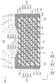
- FIG. 11 is an external perspective view showing a multilayer ceramic capacitor, which is an example of a multilayer ceramic electronic component according to the second embodiment of the present invention.
- FIG. 12 is a cross-sectional view taken along line XII-XII in FIG. 11.
- FIG. 13 is a cross-sectional view taken along line XIII-XIII in FIG. 11.
- FIG. 14 is a cross-sectional view taken along line XIV-XIV in FIG. 11.
- FIG. 15 is a cross-sectional view taken along line XV-XV in FIG. 11.
- FIG. 16 is a cross-sectional view taken along line XVI-XVI in FIG. 11.
- FIG. 17 is an exploded perspective view of the laminate shown in FIG. 1.
- the multilayer ceramic capacitor 510 includes a laminate 512 and external electrodes 524, 525.
- the laminate 512 includes a plurality of ceramic layers 514 and a plurality of internal electrode layers 516.
- the laminate 512 has a first main surface 512a and a second main surface 512b that face each other in a height direction x, a first side surface 512c and a second side surface 512d that face each other in a width direction y perpendicular to the height direction x, and a third side surface 512e and a fourth side surface 512f that face each other in a length direction z perpendicular to the height direction x and the width direction y.
- the first main surface 512a and the second main surface 512b extend along the width direction y and the length direction z, respectively.
- the first side surface 512c and the second side surface 512d extend along the height direction x and the length direction z, respectively.
- the third side surface 512e and the fourth side surface 512f extend along the height direction x and the width direction y, respectively. Therefore, the height direction x is the direction connecting the first main surface 512a and the second main surface 512b, the width direction y is the direction connecting the first side surface 512c and the second side surface 512d, and the length direction z is the direction connecting the third side surface 512e and the fourth side surface 512f.
- the corners and ridges of the laminate 512 are rounded.
- the corners are the portions where three faces of the laminate 512 intersect, and the ridges are the portions where two faces of the laminate 512 intersect.
- the laminate 512 has an effective layer portion 515a in which multiple internal electrode layers 516 face each other in the height direction x connecting the first main surface 512a and the second main surface 512b, a first outer layer portion 515b1 formed from multiple ceramic layers 514 located between the internal electrode layer 516 located closest to the first main surface 512a and the first main surface 512a, and a second outer layer portion 515b2 formed from multiple ceramic layers 514 located between the internal electrode layer 516 located closest to the second main surface 512b and the second main surface 512b.
- the first outer layer 515b1 is located on the first main surface 512a side of the laminate 512, and is an assembly of multiple ceramic layers 514 located between the first main surface 512a and the internal electrode layer 516 closest to the first main surface 512a.
- the second outer layer 515b2 is located on the second main surface 512b side of the laminate 512, and is an assembly of multiple ceramic layers 514 located between the second main surface 512b and the internal electrode layer 516 closest to the second main surface 512b.
- the area sandwiched between the first outer layer 515b1 and the second outer layer 515b2 is the effective layer 515a.
- the ceramic layer 514 may be formed of, for example, a dielectric material.
- a dielectric ceramic composed of a main component such as BaTiO 3 , CaTiO 3 , SrTiO 3 , or CaZrO 3 may be used as the dielectric material.
- a material containing a subcomponent such as a Mn compound, an Fe compound, a Cr compound, a Co compound, or a Ni compound, in a smaller amount than the main component may be used.
- the ceramic layer 514 may have a plurality of crystal grains including a perovskite-type compound having a BaTiO 3 basic structure.
- the internal electrode layer 516 includes a plurality of first internal electrode layers 516a and a plurality of second internal electrode layers 516b.
- the first internal electrode layers 516a and the second internal electrode layers 516b are alternately laminated with the ceramic layers 514 interposed therebetween.
- the first internal electrode layer 516a is disposed on the surface of the ceramic layer 514.
- the first internal electrode layer 516a faces the first main surface 512a and the second main surface 512b, has a first opposing electrode portion 518a facing the second internal electrode layer 516b, and is laminated in the direction connecting the first main surface 512a and the second main surface 512b.
- the second internal electrode layer 516b is disposed on a surface of a ceramic layer 514 different from the ceramic layer 514 on which the first internal electrode layer 516a is disposed.
- the second internal electrode layer 516b has a second opposing electrode portion 518b that faces the first main surface 512a and the second main surface 512b, and is laminated in a direction connecting the first main surface 512a and the second main surface 512b.
- the first internal electrode layer 516a is drawn out to the first side 512c and third side 512e of the laminate 512 by the first lead-out electrode portion 520a, and is drawn out to the second side 512d and fourth side 512f of the laminate 512 by the second lead-out electrode portion 520b.
- the width of the first lead-out electrode portion 520a drawn out to the first side 512c may be approximately equal to the width of the first lead-out electrode portion 520a drawn out to the third side 512e
- the width of the second lead-out electrode portion 520b drawn out to the second side 512d may be approximately equal to the width of the second lead-out electrode portion 520b drawn out to the fourth side 512f.
- the first extraction electrode portion 520a is extracted to the third side surface 512e of the laminate 512
- the second extraction electrode portion 520b is extracted to the fourth side surface 512f of the laminate 512.
- the first extraction electrode portion 520a may be extracted only to the third side surface 512e
- the second extraction electrode portion 520b may be extracted only to the fourth side surface 512f.
- the second internal electrode layer 516b is drawn out to the first side 512c and the fourth side 512f of the laminate 512 by the third draw-out electrode portion 521a, and drawn out to the second side 512d and the third side 512e of the laminate 512 by the fourth draw-out electrode portion 521b.
- the width of the third draw-out electrode portion 521a drawn out to the first side 512c may be approximately equal to the width of the third draw-out electrode portion 521a drawn out to the fourth side 512f
- the width of the fourth draw-out electrode portion 521b drawn out to the second side 512d may be approximately equal to the width of the fourth draw-out electrode portion 521b drawn out to the third side 512e.
- the third extraction electrode portion 521a is extracted to the fourth side surface 512f side of the laminate 512
- the fourth extraction electrode portion 521b is extracted to the third side surface 512e side of the laminate 512.
- the third extraction electrode portion 521a may be extracted only to the fourth side surface 512f
- the fourth extraction electrode portion 521b may be extracted only to the third side surface 512e.
- a straight line connecting the first extraction electrode portion 520a and the second extraction electrode portion 520b of the first internal electrode layer 516a intersects with a straight line connecting the third extraction electrode portion 521a and the fourth extraction electrode portion 521b of the second internal electrode layer 516b.
- the first extraction electrode portion 520a of the first internal electrode layer 516a and the fourth extraction electrode portion 521b of the second internal electrode layer 516b are preferably drawn out to opposing positions, and the second extraction electrode portion 520b of the first internal electrode layer 516a and the third extraction electrode portion 521a of the second internal electrode layer 516b are preferably drawn out to opposing positions.
- the laminate 512 also includes a side portion (W gap) 522a of the laminate 512 formed between one end in the width direction y of the first opposing electrode portion 518a and the first side surface 512c, and between the other end in the width direction y of the second opposing electrode portion 518b and the second side surface 512d.
- W gap side portion
- the laminate 512 includes a side portion (L gap) 522b of the laminate 512 formed between one end in the length direction z of the first opposing electrode portion 518a and the third side surface 512e, and between the other end in the length direction z of the second opposing electrode portion 518b and the fourth side surface 512f.
- the internal electrode layer 516 can be made of an appropriate conductive material, such as, but not limited to, metals such as Ni, Cu, Ag, Pd, and Au, or alloys containing at least one of these metals, such as Ag-Pd alloys.
- External electrodes 524, 525 are disposed on the laminate 512 as shown in FIGS.
- the external electrode 524 includes a base electrode layer 526 and a plating layer 528 formed to cover the base electrode layer 526.
- the external electrode 525 includes a base electrode layer 527 and a plating layer 529 formed to cover the base electrode layer 527.
- the external electrode 524 has a first external electrode 524a and a second external electrode 524b.
- the first external electrode 524a is arranged so as to cover the first lead-out electrode portion 520a on the first side surface 512c and the third side surface 512e, and is arranged so as to cover a portion of the first main surface 512a.
- the first external electrode 524a is electrically connected to the first lead-out electrode portion 520a of the first internal electrode layer 516a.
- the second external electrode 524b is arranged so as to cover the second extraction electrode portion 520b on the second side surface 512d and the fourth side surface 512f, and is arranged so as to cover a portion of the first main surface 512a.
- the second external electrode 524b is electrically connected to the second extraction electrode portion 520b of the first internal electrode layer 516a.
- the external electrode 525 has a third external electrode 525a and a fourth external electrode 525b.
- the third external electrode 525a is arranged so as to cover the third extraction electrode portion 521a on the first side surface 512c and the fourth side surface 512f, and is arranged so as to cover a part of the first main surface 512a.
- the third external electrode 525a is electrically connected to the third extraction electrode portion 521a of the second internal electrode layer 516b.
- the fourth external electrode 525b is arranged so as to cover the fourth extraction electrode portion 521b on the second side surface 512d and the third side surface 512e, and is arranged so as to cover a part of the first main surface 512a.
- the fourth external electrode 525b is electrically connected to the fourth extraction electrode portion 521b of the second internal electrode layer 516b.
- the first opposing electrode portion 518a of the first internal electrode layer 516a and the second opposing electrode portion 518b of the second internal electrode layer 516b face each other via the ceramic layer 514, forming a capacitance. Therefore, a capacitance can be obtained between the first external electrode 524a and the second external electrode 524b to which the first internal electrode layer 516a is connected, and the third external electrode 525a and the fourth external electrode 525b to which the second internal electrode layer 516b is connected, and the characteristics of a capacitor are expressed.
- the base electrode layer 526 includes a first base electrode layer 526a and a second base electrode layer 526b.
- the base electrode layer 527 has a third base electrode layer 527a and a fourth base electrode layer 527b.
- Each of the first base electrode layer 526a, the second base electrode layer 526b, the third base electrode layer 527a, and the fourth base electrode layer 527b has a first main surface electrode portion, a second main surface electrode portion, a third main surface electrode portion, and a fourth main surface electrode portion.
- the first base electrode layer 526a has a configuration in which the first main surface electrode portion 526a1, the second main surface electrode portion 526a2, the third main surface electrode portion 526a3, and the fourth main surface electrode portion 526a4 are stacked.
- the second base electrode layer 526b has a configuration in which the first main surface electrode portion 526b1, the second main surface electrode portion 526b2, the third main surface electrode portion 526b3, and the fourth main surface electrode portion 526b4 are stacked.
- the third base electrode layer 527a has a configuration in which a first principal surface electrode portion 527a1, a second principal surface electrode portion 527a2, a third principal surface electrode portion 527a3, and a fourth principal surface electrode portion 527a4 are stacked.
- the fourth base electrode layer 527b has a configuration in which a first principal surface electrode portion 527b1, a second principal surface electrode portion 527b2, a third principal surface electrode portion 527b3, and a fourth principal surface electrode portion 527b4 are stacked.
- the first principal surface electrode portion 526a1 is arranged on the surface of the laminate 512
- the second principal surface electrode portion 526a2 is arranged on the surface of the first principal surface electrode portion 526a1
- the third principal surface electrode portion 526a3 is arranged on the surface of the second principal surface electrode portion 526a2
- the fourth principal surface electrode portion 526a4 is arranged on the surface of the third principal surface electrode portion 526a3.
- a direction is defined on the first principal surface 512a that connects the end portion of the first principal surface electrode portion of the first base electrode layer toward the center of the laminate to the surface at which the first internal electrode layer is exposed on the surface of the laminate, specifically, a direction that connects the first end portion 526a1t toward the center of the laminate 512 of the first principal surface electrode portion 526a1 of the first base electrode layer 526a to the first side surface 512c of the laminate 512 at which the first extraction electrode portion 520a of the first internal electrode layer 516a is exposed (hereinafter, the third reference direction).
- the relationship in length between the first principal surface electrode portion 526a1, the second principal surface electrode portion 526a2, the third principal surface electrode portion 526a3, and the fourth principal surface electrode portion 526a4 of the first base electrode layer 526a is the same as the above configuration shown in FIG. 14 even when viewed in the LT cross section.
- the first end 526a1t, the second end 526a2t, the third end 526a3t, and the fourth end 526a4t of the first base electrode layer 526a on the central side of the laminate 512 are not aligned with each other, so that the stress of the first external electrode 524a toward the central side of the laminate 512 that occurs during solder shrinkage can be dispersed.
- a direction connecting the end portion on the central side of the laminate of the first principal surface electrode portion of the fourth base electrode layer to the surface at which the second internal electrode layer is exposed on the surface of the laminate specifically, a direction connecting the first end portion 527b1t on the central side of the laminate 512 of the first principal surface electrode portion 527b1 of the fourth base electrode layer 527b to the third side surface 512e of the laminate 512 at which the second extraction electrode portion 520b of the second internal electrode layer 516b is exposed, is determined (hereinafter, the fourth reference direction).
- the relationship in length between the first principal surface electrode portion 527b1, the second principal surface electrode portion 527b2, the third principal surface electrode portion 527b3, and the fourth principal surface electrode portion 527b4 of the fourth base electrode layer 527b is the same as the above configuration shown in FIG. 14 even when viewed in the LT cross section.
- the first principal surface electrode portion 527b1, the second principal surface electrode portion 527b2, the third principal surface electrode portion 527b3, and the fourth principal surface electrode portion 527b4 of the fourth base electrode layer 527b have first end portions 527b1t, second end portions 527b2t, third end portions 527b3t, and fourth end portions 527b4t on the central side of the laminate 512 that are not aligned with each other, so that the stress of the third external electrode 525a toward the central side of the laminate 512 that occurs during solder shrinkage can be dispersed.
- a direction is determined that connects the end portion of the first principal surface electrode portion of the second base electrode layer toward the center of the laminate to the surface at which the first internal electrode layer is exposed on the surface of the laminate, specifically, a direction that connects the first end portion 526b1t toward the center of the laminate 512 of the first principal surface electrode portion 526b1 of the second base electrode layer 526b to the fourth side surface 512f of the laminate 512 at which the first extraction electrode portion 520a of the first internal electrode layer 516a is exposed (hereinafter, the fifth reference direction).
- the relationship in length between the first principal surface electrode portion 526b1, the second principal surface electrode portion 526b2, the third principal surface electrode portion 526b3, and the fourth principal surface electrode portion 526b4 of the second base electrode layer 526b is the same as the above configuration shown in FIG. 15 even when viewed in the LT cross section.
- the first principal surface electrode portion 526b1, the second principal surface electrode portion 526b2, the third principal surface electrode portion 526b3, and the fourth principal surface electrode portion 526b4 of the second base electrode layer 526b have first end 526b1t, second end 526b2t, third end 526b3t, and fourth end 526b4t on the central side of the laminate 512 that are not aligned with each other, so that the stress of the second external electrode 524b toward the central side of the laminate 512 that occurs during solder shrinkage can be dispersed.
- a direction connecting the end portion of the first principal surface electrode portion of the third base electrode layer toward the center of the laminate to the surface at which the second internal electrode layer is exposed on the surface of the laminate specifically, a direction connecting the first end portion 527a1t toward the center of the laminate 512 of the first principal surface electrode portion 527a1 of the third base electrode layer 527a to the third side surface 512e of the laminate 512 at which the third extraction electrode portion 521a of the second internal electrode layer 516b is exposed, is determined (hereinafter, the sixth reference direction).
- the relationship in length between the first principal surface electrode portion 527a1, the second principal surface electrode portion 527a2, the third principal surface electrode portion 527a3, and the fourth principal surface electrode portion 527a4 of the third base electrode layer 527a is the same as the above configuration shown in FIG. 15 even when viewed in the LT cross section.
- the first principal surface electrode portion 527a1, the second principal surface electrode portion 527a2, the third principal surface electrode portion 527a3, and the fourth principal surface electrode portion 527a4 of the third base electrode layer 527a have first end portion 526a1t, second end portion 526a2t, third end portion 526a3t, and fourth end portion 526a4t on the central side of the laminate 512 that are not aligned with each other, so that the stress of the fourth external electrode 525b toward the central side of the laminate 512 that occurs during solder shrinkage can be dispersed.
- the first end 526a1t of the first principal surface electrode portion 526a1 is not covered by the second principal surface electrode portion 526a2, the second end 526a2t of the second principal surface electrode portion 526a2 is not covered by the third principal surface electrode portion 526a3, and the third end 526a3t of the third principal surface electrode portion 526a3 is not covered by the fourth principal surface electrode portion 526a4.
- the stress acting on the first end 526a1t to the fourth end 526a4t of each of the first principal surface electrode portion 526a1 to the fourth principal surface electrode portion 526a4 can be concentrated toward the outside of the laminate 512 (the first side surface 512c side and the third side surface 512e side) rather than at these ends, dispersing the stress and improving the mechanical strength.
- the first end 527b1t of the first principal surface electrode portion 527b1 is not covered by the second principal surface electrode portion 527b2
- the second end 527b2t of the second principal surface electrode portion 527b2 is not covered by the third principal surface electrode portion 527b3
- the third end 527b3t of the third principal surface electrode portion 527b3 is not covered by the fourth principal surface electrode portion 527b4.
- the stress acting on the first end 527b1t to the fourth end 527b4t of each of the first principal surface electrode portion 527b1 to the fourth principal surface electrode portion 527b4 can be concentrated toward the outside of the laminate 512 (the second side surface 512d side and the third side surface 512e side) rather than at these ends, dispersing the stress and improving the mechanical strength.
- the first end 527a1t of the first principal surface electrode portion 527a1 is not covered by the second principal surface electrode portion 527a2, the second end 527a2t of the second principal surface electrode portion 527a2 is not covered by the third principal surface electrode portion 527a3, and the third end 527a3t of the third principal surface electrode portion 527a3 is not covered by the fourth principal surface electrode portion 527a4.
- the stress acting on the first end 527a1t to the fourth end 527a4t of each of the first principal surface electrode portion 527a1 to the fourth principal surface electrode portion 527a4 can be concentrated toward the outside of the laminate 512 (the first side surface 512c side and the fourth side surface 512f side) rather than at these ends, dispersing the stress and improving the mechanical strength.
- the first end 526b1t of the first principal surface electrode portion 526b1 is not covered by the second principal surface electrode portion 526b2, the second end 526b2t of the second principal surface electrode portion 526b2 is not covered by the third principal surface electrode portion 526b3, and the third end 526b3t of the third principal surface electrode portion 526b3 is not covered by the fourth principal surface electrode portion 526b4.
- the stress acting on the first end 526b1t to the fourth end 526b4t of each of the first to fourth principal surface electrode portions 526b1 to 526b4 can be concentrated toward the outside of the laminate 512 (the second side surface 512d side and the fourth side surface 512f side) rather than at these ends, dispersing the stress and improving the mechanical strength.
- the fourth principal surface electrode portion 526a4 of the first underlying electrode layer 526a, the fourth principal surface electrode portion 526b4 of the second underlying electrode layer 526b, the fourth principal surface electrode portion 527a4 of the third underlying electrode layer 527a, and the fourth principal surface electrode portion 527b4 of the fourth underlying electrode layer 527b may each be exposed on the surface of the multilayer ceramic capacitor 110 as the outermost layer.
- the solder will not wet to the fourth ends 526a4t, 526b4t, 527a4t, and 527b4t on the central side of the laminate 512 when the laminated ceramic capacitor 110 is mounted, thereby suppressing short circuit defects.
- fourth principal surface electrode portion 526a4, the fourth principal surface electrode portion 526b4, the fourth principal surface electrode portion 527a4, and the fourth principal surface electrode portion 527b4 may be covered with a plating layer, as in the examples shown in Figures 12 to 15.
- the first to fourth main surface electrode portions constituting the base electrode layers 526 and 527 can be formed by a thin film formation method such as sputtering or vapor deposition, or by screen printing.
- a thin film formation method such as sputtering or vapor deposition, or by screen printing.
- the details of these methods are the same as those in the first embodiment, and a detailed description will be omitted.
- the plating layer 528 includes a first plating layer 528a and a second plating layer 528b.
- the first plating layer 528a is arranged to cover the first principal surface electrode portion 526a1 to the fourth principal surface electrode portion 526a4 as the first base electrode layer 526a.
- the second plating layer 528b is arranged to cover the first principal surface electrode portion 526b1 to the fourth principal surface electrode portion 526b4 as the second base electrode layer 526b.
- the plating layer 528 is formed of multiple layers. That is, the plating layer 528 has an underplating layer 530 and a top plating layer 532.
- the underplating layer 530 includes a first underplating layer 530a included in the first plating layer 528a and a second underplating layer 530b included in the second plating layer 528b.
- the top plating layer 532 includes a first top plating layer 532a included in the first plating layer 528a and a second top plating layer 532b included in the second plating layer 528b.
- the first underplating layer 530a of the underplating layer 530 is arranged to cover the fourth principal surface electrode portion 526a4 of the first base electrode layer 526a.
- the second underplating layer 530b of the underplating layer 530 is arranged to cover the fourth main surface electrode portion 526b4 of the second underelectrode layer 526b.
- the surface plating layer 532 may be formed of multiple layers.
- the surface plating layer 532 has a two-layer structure consisting of a middle plating layer 534, which is a Ni plating layer, and an upper plating layer 536, which is a Sn plating layer.
- the first intermediate plating layer 534a covers the first bottom plating layer 530a
- the first top plating layer 536a covers the first intermediate plating layer 534a
- the second intermediate plating layer 534b covers the second bottom plating layer 530b
- the second top plating layer 536b covers the second intermediate plating layer 534b.
- the plating layer 529 includes a third plating layer 529a and a fourth plating layer 529b.
- the plating layer 529 is formed of multiple layers. That is, the plating layer 529 has an underplating layer 531 and a top plating layer 533.
- the underplating layer 531 includes a first underplating layer 531a included in the third plating layer 529a and a second underplating layer 531b included in the fourth plating layer 529b.
- the top plating layer 533 includes a first top plating layer 533a included in the third plating layer 529a and a second top plating layer 533b included in the fourth plating layer 529b.
- the first underplating layer 531a of the underplating layer 531 is arranged to cover the fourth principal surface electrode portion 527a4 of the third underelectrode layer 527a.
- the second underplating layer 531b of the underplating layer 531 is arranged to cover the fourth principal surface electrode portion 527b4 of the fourth underelectrode layer 527b.
- the surface plating layer 533 may be formed of multiple layers.
- the surface plating layer 533 has a two-layer structure consisting of a middle plating layer 535, which is a Ni plating layer, and an upper plating layer 537, which is a Sn plating layer.
- the first intermediate plating layer 535a covers the first lower plating layer 531a
- the first upper plating layer 537a covers the first intermediate plating layer 535a
- the second intermediate plating layer 535b covers the second lower plating layer 531b
- the second upper plating layer 537b covers the second intermediate plating layer 535b.
- the underplating layers 530, 531 preferably contain at least one metal selected from, for example, Cu, Ni, Sn, Pb, Au, Ag, Pd, Bi, or Zn, or an alloy containing such a metal.
- the underplating layers 530, 531 are preferably Cu plating layers.
- the middle plating layers 534, 535 as Ni plating layers can prevent the lower plating layers 530, 531 from being eroded by solder when mounting the multilayer ceramic capacitor 110. Furthermore, the upper plating layers 536, 537 as Sn plating layers improve the wettability of the solder when mounting the multilayer ceramic capacitor 110, making mounting easier. If the plating layers 528, 529 have a three-layer structure, in addition to the above, it is preferable that they are laminated in the order of Sn plating layer, Ni plating layer, and Sn plating layer.
- the ratio of the W dimension to the L dimension is 0.85 or more and 1.00 or less, but the ratio of the W dimension to the L dimension may be any other value.
- the multilayer ceramic capacitor 510 shown in FIG. 11, which has the above-mentioned configuration, has the same effect as the multilayer ceramic capacitor 10 of the first embodiment. Also, like the first embodiment, the effect of this invention is more pronounced when the T dimension of the multilayer ceramic capacitor 510 is 150 ⁇ m or less. Furthermore, when the T dimension is 50 ⁇ m or less, the multilayer ceramic capacitor 10 is thinned, and reliability in mechanical strength becomes even more necessary, so the effect of this invention is more pronounced.
- the external electrodes 524 and 525 of the multilayer ceramic capacitor 510 have the first to fourth modified examples similar to the external electrodes 24 of the first to fourth modified examples of the multilayer ceramic capacitor 10 according to the first embodiment.
- a dielectric sheet and a conductive paste for the internal electrodes are prepared.
- the dielectric sheet and the conductive paste for the internal electrode layers contain a binder (e.g., a known organic binder) and a solvent (e.g., a known organic binder).
- a binder e.g., a known organic binder
- a solvent e.g., a known organic binder
- a conductive paste for the internal electrodes is printed in a predetermined pattern on the dielectric sheet, for example by screen printing or gravure printing, to form an internal electrode pattern.
- a conductive paste layer is formed by applying a paste made of a conductive material onto the dielectric sheet by a method such as the printing method described above.
- the paste made of a conductive material is, for example, a metal powder to which an organic binder and an organic solvent have been added.
- an outer layer dielectric sheet on which no internal electrode pattern is printed is also produced.
- a screen plate for printing the first internal electrode layer 516a and a screen plate for printing the second internal electrode layer 516b are prepared separately, and the internal electrode layers of the present invention can be printed using a printer capable of printing the two types of screen plates separately.
- the laminated sheet is produced using the dielectric sheets on which these internal electrode patterns are formed. That is, a predetermined number of dielectric sheets for the outer layer on which no internal electrode pattern is formed are laminated to form a portion that will become the first outer layer portion 515b1 on the first main surface 512a side.
- dielectric sheets on which an internal electrode pattern corresponding to the first internal electrode layer 516a is formed and dielectric sheets on which an internal electrode pattern corresponding to the second internal electrode layer 516b is formed are alternately laminated to form a portion that will become the effective layer portion 515a, and further on top of that, a predetermined number of dielectric sheets for the outer layer on which no internal electrode pattern is formed are laminated to form a portion that will become the second outer layer portion 515b2. In this way, the laminated sheet is produced.
- the laminated sheets are pressed in the lamination direction using a means such as a hydrostatic press to create a laminated block.
- the laminated block is cut to the specified size and laminated chips are cut out. After this, wet barreling is performed to round the corners and edges of the laminated chips.
- the firing temperature depends on the ceramic and internal electrode materials, but is preferably 900°C or higher and 1400°C or lower.
- base electrode layers 526, 527 consisting of a first principal surface electrode portion, a second principal surface electrode portion, a third principal surface electrode portion, and a fourth principal surface electrode portion are formed on parts of the first principal surface 512a and the second principal surface 512b, as well as the first side surface 512c, the second side surface 512d, the third side surface 512e, and the fourth side surface 512f of the laminate 512.
- the first to fourth main surface electrode portions are formed by sputtering or screen printing, as in the first embodiment.
- the sputtered film is dissolved using an etching solution. This removes the sputtered film from the laminate 512 except for the areas covered with the resin mask.
- the mask in this process is formed so that the length along the direction connecting the end of the first main surface electrode portion of the base electrode layer of the laminate 512 on the central side of the laminate 512 to the surface of the laminate 512 where each of the first internal electrode layer 516a and the second internal electrode layer 516b is exposed is shorter than that formed in the previous process (2-2).
- the sputtered film obtained in the above step (2-6) is dissolved using an etching solution. This removes the sputtered film from the laminate 512 except for the area covered with the resin mask.
- the third and fourth main surface electrode portions are successively formed by repeating the above steps (2-5) through (2-9).
- the mask in step (2-5) for successively forming the third and fourth main surface electrode portions is formed so that the length along the direction connecting the end of the first main surface electrode portion of the base electrode layer of the laminate 512 on the center side of the laminate 512 to the surface of the laminate 512 where the first internal electrode layer 516a and the second internal electrode layer 516b are exposed is longer than that formed in the previous step (2-5).
- the length of the first principal surface electrode portion 527b1 is length A
- the length of the second principal surface electrode portion 527b2 is length B
- the length of the third principal surface electrode portion 527b3 is length C
- the length of the fourth principal surface electrode portion 527b4 is length D
- the length of the first principal surface electrode portion 526b1 is length A
- the length of the second principal surface electrode portion 526b2 is length B
- the length of the third principal surface electrode portion 526b3 is length C
- the length of the fourth principal surface electrode portion 526b4 is length D
- the length of the first principal surface electrode portion 527a1 is length A
- the length of the second principal surface electrode portion 527a2 is length B
- the length of the third principal surface electrode portion 527a3 is length C
- the length of the fourth principal surface electrode portion 527a4 is length D
- the resin masks obtained in the above steps (2-2) and (2-7) are formed so as not to cover the first side surface 512c, the second side surface 512d, the third side surface 512e and the fourth side surface 512f of the laminate 512.
- the opposing distance between the pair of printed patterns in each of the width direction y and length direction z formed on the first main surface 512a of the laminate 512 is such that the length along the direction connecting the end of the first main surface electrode portion of the base electrode layer toward the center of the laminate to the surface where the first internal electrode layer is exposed on the surface of the laminate 512 is longer for the one formed earlier than the one formed later for each of the formation of the first main surface electrode portion, the formation of the second main surface electrode portion, the formation of the third main surface electrode portion, and the formation of the fourth main surface electrode portion.
- the first to fourth main surface electrode portions are formed in the same configuration as the multilayer ceramic capacitor 510 shown in Figures 14 and 15, as in the case of formation by sputtering.
- plating layers 528, 529 are formed on the surfaces of the fourth principal surface electrode portions of the base electrode layers 526, 527.
- the plating layers 528, 529 are formed, for example, by barrel plating.
- each plating layer is formed in sequence, for example, by barrel plating.
- plating layer 528 is to be formed directly as a plating layer, the procedure is as follows.
- the first side surface 512c to the fourth side surface 512f of the laminate 512 are plated to form a plating film directly on the exposed portions of the first lead electrode portion 520a and the second lead electrode portion 520b of the internal electrode layer 516.
- Either electrolytic plating or electroless plating may be used for plating, but electroless plating has the disadvantage of requiring pretreatment with a catalyst or the like to improve the plating deposition rate, which complicates the process. Therefore, electrolytic plating is usually preferred. Barrel plating is preferred as a plating method.
- the plating layer 528 as a direct plating layer may be formed in multiple layers, for example, as in the laminated ceramic capacitor 310 shown in FIG. 9, and an upper layer plating electrode formed on the surface of a lower layer plating electrode may be formed in the same manner.
- the multilayer ceramic capacitor 510 shown in Figure 11 can be manufactured.
- the ends of the first to fourth main surface electrode portions formed on the first main surface of the laminate are arranged so as not to align, thereby dispersing the locations where stress occurs and preventing cracks from propagating from the tips of the external electrodes into the interior of the multilayer ceramic capacitor.
- Fig. 18 is an external perspective view showing a multilayer ceramic capacitor, which is an example of a multilayer ceramic electronic component according to the third embodiment of the present invention.
- Fig. 19 is a schematic cross-sectional view taken along line XIX-XIX in Fig. 18.
- Fig. 20 is a schematic cross-sectional view taken along line XX-XX in Fig. 18.
- the same reference numerals are used for configurations that are the same as or correspond to those of the multilayer ceramic capacitor 10 according to the first embodiment shown in Figs. 1 to 10, and detailed description thereof will be omitted.
- the multilayer ceramic capacitor 610 according to the third embodiment of the present invention has a laminate 12 and an external electrode 24 that have the same configuration as the multilayer ceramic capacitor 10 according to the first embodiment. However, the multilayer ceramic capacitor 610 has the L dimension and the W dimension swapped with respect to the multilayer ceramic capacitor 10 according to the first embodiment.
- the dimensions of the multilayer ceramic capacitor 610 are such that the L dimension in the length direction z is 0.1 mm or more and 2.5 mm or less, the T dimension in the height direction x is 0.04 mm or more and 2.5 mm or less, and the W dimension in the width direction y is 0.2 mm or more and 3.2 mm or less.
- the external electrode 24 of the multilayer ceramic capacitor 610 has the first to fourth modified examples similar to the external electrode 24 of the first to fourth modified examples of the multilayer ceramic capacitor 10 according to the first embodiment.
- the method for manufacturing the multilayer ceramic capacitor according to the third embodiment is the same as the method for manufacturing the multilayer ceramic capacitor according to the first embodiment.
- the multilayer ceramic capacitor 10 according to the first embodiment is manufactured so that the L dimension and the W dimension are swapped.
- the multilayer ceramic capacitor 610 shown in Figure 18 can be manufactured.
- the ends of the first to fourth main surface electrode portions formed on the first main surface of the laminate are arranged so as not to align, thereby dispersing the locations where stress occurs and preventing cracks from propagating from the tips of the external electrodes into the interior of the multilayer ceramic capacitor.
- a laminate including a plurality of laminated ceramic layers, the laminate including first and second main faces facing each other in a lamination direction of the plurality of ceramic layers, first and second side faces facing each other in a width direction perpendicular to the lamination direction, a first end face and a second end face facing each other in a length direction perpendicular to the lamination direction and the width direction, first internal electrode layers stacked alternately with the plurality of ceramic layers and exposed at the first end faces, and second internal electrode layers stacked alternately with the plurality of ceramic layers and exposed at the second end faces; a first external electrode covering a portion of the first main surface and at least a portion of the first end surface of the laminate; a second external electrode covering a portion of the first main surface and at least a portion of the second end surface of the laminate;
- Each of the first external electrode and the second external electrode has a first principal surface electrode portion disposed on the first principal surface; a second principal surface electrode portion disposed on a portion of the first principal surface electrode portion; a third
- ⁇ 2> In a direction from the center of the laminate to any one of the faces of the first internal electrode layer or the second internal electrode layer exposed on the surface of the laminate, an end portion of the first principal surface electrode portion on a center side of the laminate is not covered by the second principal surface electrode portion; an end portion of the second principal surface electrode portion on a center side of the laminate is not covered by the third principal surface electrode portion;
- the thickness of the first principal surface electrode portion is 10 ⁇ m or less
- the thickness of the second principal surface electrode portion is 10 ⁇ m or less
- the third principal surface electrode portion has a thickness of 10 ⁇ m or less
- ⁇ 4> The multilayer ceramic capacitor according to any one of ⁇ 1> to ⁇ 3>, wherein the first principal surface electrode portion contains a component similar to a main component of the ceramic layers.
- the second principal surface electrode portion contains a component similar to a main component of the ceramic layer
- the first principal surface electrode portion is disposed so as to wrap around a plane perpendicular to the first principal surface
- the second principal surface electrode portion is disposed so as to wrap around a plane perpendicular to the first principal surface
- the third principal surface electrode portion is disposed around a plane perpendicular to the first principal surface
- ⁇ 7> In a direction connecting the first main surface and the second main surface, The multilayer ceramic capacitor according to any one of ⁇ 1> to ⁇ 6>, wherein the thickness of the laminate is 150 ⁇ m or less.
- ⁇ 8> In a direction connecting the first main surface and the second main surface, The multilayer ceramic capacitor according to any one of ⁇ 1> to ⁇ 6>, wherein the thickness of the laminate is 50 ⁇ m or less.
- ⁇ 10> The multilayer ceramic capacitor according to any one of ⁇ 1> to ⁇ 9>, wherein the dimension in the length direction is greater than the dimension in the width direction.
- ⁇ 11> The multilayer ceramic capacitor according to any one of ⁇ 1> to ⁇ 9>, wherein the dimension in the width direction is greater than the dimension in the length direction.
- a laminate including a plurality of stacked ceramic layers including a plurality of stacked ceramic layers, the laminate including a first main surface and a second main surface facing each other in a stacking direction of the plurality of ceramic layers, a first side surface and a second side surface facing each other in a width direction perpendicular to the stacking direction, a third side surface and a fourth side surface facing each other in a length direction perpendicular to the stacking direction and the width direction, first internal electrode layers stacked alternately with the plurality of ceramic layers and exposed at least to the third side surface and the fourth side surface, and a second internal electrode layer stacked alternately with the plurality of ceramic layers and exposed at least to the fourth side surface and the third side surface; a first external electrode covering a portion of the first main surface and at least a portion of the third side surface of the laminate; a second external electrode covering a portion of the first main surface and at least a portion of the fourth side surface of the laminate; a third external electrode covering a portion of the first main surface and at
- ⁇ 13> The multilayer ceramic capacitor according to ⁇ 12>, wherein a ratio of a dimension in the width direction to a dimension in the length direction is 0.85 or more and 1.00 or less.
Landscapes
- Engineering & Computer Science (AREA)
- Power Engineering (AREA)
- Manufacturing & Machinery (AREA)
- Microelectronics & Electronic Packaging (AREA)
- Chemical & Material Sciences (AREA)
- Ceramic Engineering (AREA)
- Inorganic Chemistry (AREA)
- Fixed Capacitors And Capacitor Manufacturing Machines (AREA)
- Ceramic Capacitors (AREA)
Priority Applications (4)
| Application Number | Priority Date | Filing Date | Title |
|---|---|---|---|
| KR1020257031637A KR20250153270A (ko) | 2023-04-18 | 2024-01-18 | 적층 세라믹 콘덴서 |
| CN202480025328.0A CN120937098A (zh) | 2023-04-18 | 2024-01-18 | 层叠陶瓷电容器 |
| JP2025515053A JPWO2024219030A1 (https=) | 2023-04-18 | 2024-01-18 | |
| US19/272,117 US20250343008A1 (en) | 2023-04-18 | 2025-07-17 | Multilayer ceramic capacitor |
Applications Claiming Priority (2)
| Application Number | Priority Date | Filing Date | Title |
|---|---|---|---|
| JP2023-067728 | 2023-04-18 | ||
| JP2023067728 | 2023-04-18 |
Related Child Applications (1)
| Application Number | Title | Priority Date | Filing Date |
|---|---|---|---|
| US19/272,117 Continuation US20250343008A1 (en) | 2023-04-18 | 2025-07-17 | Multilayer ceramic capacitor |
Publications (1)
| Publication Number | Publication Date |
|---|---|
| WO2024219030A1 true WO2024219030A1 (ja) | 2024-10-24 |
Family
ID=93152541
Family Applications (1)
| Application Number | Title | Priority Date | Filing Date |
|---|---|---|---|
| PCT/JP2024/001184 Ceased WO2024219030A1 (ja) | 2023-04-18 | 2024-01-18 | 積層セラミックコンデンサ |
Country Status (5)
| Country | Link |
|---|---|
| US (1) | US20250343008A1 (https=) |
| JP (1) | JPWO2024219030A1 (https=) |
| KR (1) | KR20250153270A (https=) |
| CN (1) | CN120937098A (https=) |
| WO (1) | WO2024219030A1 (https=) |
Citations (3)
| Publication number | Priority date | Publication date | Assignee | Title |
|---|---|---|---|---|
| WO2008001542A1 (en) * | 2006-06-28 | 2008-01-03 | Murata Manufacturing Co., Ltd. | Ceramic electronic component and method for manufacturing same |
| JP2017199847A (ja) * | 2016-04-28 | 2017-11-02 | 株式会社村田製作所 | 積層セラミックコンデンサ |
| JP2020017557A (ja) * | 2018-07-23 | 2020-01-30 | 太陽誘電株式会社 | 積層セラミック電子部品、積層セラミック電子部品の製造方法及び電子部品内蔵基板 |
Family Cites Families (1)
| Publication number | Priority date | Publication date | Assignee | Title |
|---|---|---|---|---|
| JP7307547B2 (ja) | 2019-02-15 | 2023-07-12 | 太陽誘電株式会社 | 積層セラミック電子部品及び回路基板 |
-
2024
- 2024-01-18 JP JP2025515053A patent/JPWO2024219030A1/ja active Pending
- 2024-01-18 KR KR1020257031637A patent/KR20250153270A/ko active Pending
- 2024-01-18 CN CN202480025328.0A patent/CN120937098A/zh active Pending
- 2024-01-18 WO PCT/JP2024/001184 patent/WO2024219030A1/ja not_active Ceased
-
2025
- 2025-07-17 US US19/272,117 patent/US20250343008A1/en active Pending
Patent Citations (3)
| Publication number | Priority date | Publication date | Assignee | Title |
|---|---|---|---|---|
| WO2008001542A1 (en) * | 2006-06-28 | 2008-01-03 | Murata Manufacturing Co., Ltd. | Ceramic electronic component and method for manufacturing same |
| JP2017199847A (ja) * | 2016-04-28 | 2017-11-02 | 株式会社村田製作所 | 積層セラミックコンデンサ |
| JP2020017557A (ja) * | 2018-07-23 | 2020-01-30 | 太陽誘電株式会社 | 積層セラミック電子部品、積層セラミック電子部品の製造方法及び電子部品内蔵基板 |
Also Published As
| Publication number | Publication date |
|---|---|
| US20250343008A1 (en) | 2025-11-06 |
| JPWO2024219030A1 (https=) | 2024-10-24 |
| CN120937098A (zh) | 2025-11-11 |
| KR20250153270A (ko) | 2025-10-24 |
Similar Documents
| Publication | Publication Date | Title |
|---|---|---|
| US10475584B2 (en) | Electronic component mount structure, electronic component, and method for manufacturing electronic component | |
| CN113539682B (zh) | 层叠陶瓷电子部件 | |
| KR20190011219A (ko) | 적층 세라믹 콘덴서 | |
| US11342118B2 (en) | Multilayer ceramic capacitor and method of manufacturing multilayer ceramic capacitor | |
| US11495404B2 (en) | Multilayer ceramic electronic component | |
| JP2023013421A (ja) | 積層セラミック電子部品 | |
| JP2025074232A (ja) | 積層セラミックコンデンサ | |
| JP2020188081A (ja) | 積層セラミック電子部品 | |
| WO2024219030A1 (ja) | 積層セラミックコンデンサ | |
| KR102870830B1 (ko) | 적층 세라믹 전자부품 | |
| JP2024144794A (ja) | 積層セラミックコンデンサ | |
| JP7835297B2 (ja) | 積層セラミックコンデンサ | |
| JP7852745B2 (ja) | 積層セラミックコンデンサ | |
| US20260011493A1 (en) | Multilayer ceramic capacitor | |
| JP2021120976A (ja) | 保護フレーム部付き積層セラミック電子部品及びその実装構造 | |
| US20260081075A1 (en) | Multilayer ceramic capacitor | |
| US20260081072A1 (en) | Multilayer ceramic capacitor | |
| US20250329497A1 (en) | Multilayer ceramic capacitor | |
| CN216015095U (zh) | 层叠陶瓷电容器 | |
| WO2024232172A1 (ja) | 積層セラミックコンデンサ | |
| WO2025141994A1 (ja) | 積層セラミックコンデンサ | |
| WO2024018718A1 (ja) | 積層セラミック電子部品および積層セラミック電子部品の実装構造 | |
| WO2024252777A1 (ja) | 積層セラミックコンデンサ | |
| WO2025225128A1 (ja) | 積層セラミックコンデンサ | |
| JP2024162476A (ja) | 積層セラミックコンデンサ |
Legal Events
| Date | Code | Title | Description |
|---|---|---|---|
| 121 | Ep: the epo has been informed by wipo that ep was designated in this application |
Ref document number: 24792306 Country of ref document: EP Kind code of ref document: A1 |
|
| WWE | Wipo information: entry into national phase |
Ref document number: 202517063123 Country of ref document: IN |
|
| WWP | Wipo information: published in national office |
Ref document number: 202517063123 Country of ref document: IN |
|
| ENP | Entry into the national phase |
Ref document number: 2025515053 Country of ref document: JP Kind code of ref document: A |
|
| WWE | Wipo information: entry into national phase |
Ref document number: 2025515053 Country of ref document: JP |
|
| ENP | Entry into the national phase |
Ref document number: 1020257031637 Country of ref document: KR Free format text: ST27 STATUS EVENT CODE: A-0-1-A10-A15-NAP-PA0105 (AS PROVIDED BY THE NATIONAL OFFICE) |
|
| WWP | Wipo information: published in national office |
Ref document number: 1020257031637 Country of ref document: KR |
|
| NENP | Non-entry into the national phase |
Ref country code: DE |
|
| 122 | Ep: pct application non-entry in european phase |
Ref document number: 24792306 Country of ref document: EP Kind code of ref document: A1 |