WO2024218985A1 - 電子機器 - Google Patents
電子機器 Download PDFInfo
- Publication number
- WO2024218985A1 WO2024218985A1 PCT/JP2023/016003 JP2023016003W WO2024218985A1 WO 2024218985 A1 WO2024218985 A1 WO 2024218985A1 JP 2023016003 W JP2023016003 W JP 2023016003W WO 2024218985 A1 WO2024218985 A1 WO 2024218985A1
- Authority
- WO
- WIPO (PCT)
- Prior art keywords
- antenna
- slit
- substrate
- electronic device
- region
- Prior art date
- Legal status (The legal status is an assumption and is not a legal conclusion. Google has not performed a legal analysis and makes no representation as to the accuracy of the status listed.)
- Ceased
Links
Images





Classifications
-
- H—ELECTRICITY
- H01—ELECTRIC ELEMENTS
- H01Q—ANTENNAS, i.e. RADIO AERIALS
- H01Q1/00—Details of, or arrangements associated with, antennas
- H01Q1/52—Means for reducing coupling between antennas; Means for reducing coupling between an antenna and another structure
-
- H—ELECTRICITY
- H01—ELECTRIC ELEMENTS
- H01Q—ANTENNAS, i.e. RADIO AERIALS
- H01Q13/00—Waveguide horns or mouths; Slot antennas; Leaky-waveguide antennas; Equivalent structures causing radiation along the transmission path of a guided wave
- H01Q13/08—Radiating ends of two-conductor microwave transmission lines, e.g. of coaxial lines, of microstrip lines
-
- H—ELECTRICITY
- H01—ELECTRIC ELEMENTS
- H01Q—ANTENNAS, i.e. RADIO AERIALS
- H01Q21/00—Antenna arrays or systems
- H01Q21/28—Combinations of substantially independent non-interacting antenna units or systems
Definitions
- the present invention relates to an electronic device equipped with an antenna for wireless communication.
- Electronic devices are known that are equipped with antennas for wireless communication connections with other communication devices, such as wireless LAN communication based on the IEEE 802.11 standard and wireless communication based on the Bluetooth (registered trademark) standard.
- One type of such antenna is a pattern antenna formed from a conductive layer on the surface of a printed circuit board or the like.
- Some of the electronic devices mentioned above are equipped with multiple antennas. When multiple antennas are formed on a single board, these antennas may interfere with each other due to radiation currents propagating through the conductive layers on the printed board, which may adversely affect wireless communications.
- the present invention was made in consideration of the above situation, and one of its objectives is to provide an electronic device that can suppress the propagation of radiated current from an antenna mounted on a substrate.
- the electronic device comprises a substrate, a first antenna and a second antenna formed on the substrate and each performing wireless communication, a ground pattern formed by one conductive layer of the substrate, and a slit formed by cutting the conductive layer with a point on the outer periphery of the ground pattern as a base point, the first antenna is disposed in a first antenna region surrounded by the outer periphery of the substrate and the conductive layer in a planar view, the second antenna is disposed in a second antenna region surrounded by the outer periphery of the substrate and the conductive layer in a planar view, the base point of the slit is located between the first antenna region and the second antenna region in a planar view, and the slit has a portion facing the end of the first antenna region on the opposite side to the outer periphery of the substrate in a planar view.
- 1 is a perspective view showing an external appearance of a substrate incorporated in an electronic device according to an embodiment of the present invention
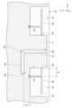
- 2 is a partial plan view of a substrate incorporated in the electronic device according to the embodiment of the present invention
- 5 is a diagram showing an example of a distribution of radiation current in the electronic device according to the embodiment of the present invention
- 11A and 11B are diagrams illustrating an example of a simulation result of inter-antenna isolation in the electronic device according to the embodiment of the present invention.
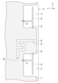
- 13 is a partial plan view of a substrate built into an electronic device according to a modified example of the present invention.
- FIG. 13 is a partial plan view of a substrate built into an electronic device according to another modified example of the present invention.
- FIG. 13 is a partial plan view of a substrate built into an electronic device according to a modified example of the present invention, in which a meandering slit is formed.
- FIG. FIG. 13 is a partial plan view of the front surface side of the substrate in a modified example of the present invention in which the antenna and the slit are formed in different conductive layers.
- 13 is a partial plan view of the rear surface side of the substrate in a modified example of the present invention in which the antenna and the slit are formed in different conductive layers.
- FIG. 13 is a partial plan view of a substrate having a plurality of slits formed therein and built into an electronic device according to a modified example of the present invention.
- the electronic device 1 is, for example, a personal computer, a stationary game machine, a portable game machine, a smartphone, etc., and includes a substrate 10, a first antenna 20, and a second antenna 30.
- FIG. 1 is a perspective view showing an example of the appearance of the substrate 10 built into the electronic device 1.
- FIG. 2 is a partial plan view showing an enlarged view of a portion of the substrate 10. Note that all figures, including the following figures, are schematic diagrams for explaining the features of the electronic device 1 according to this embodiment, and the scale, etc., differ from the actual ones. Furthermore, parts that are not directly related to the explanation in this specification have been omitted as appropriate.
- the substrate 10 is an electronic circuit board on which various circuit elements for implementing the functions of the electronic device 1 are mounted.
- the substrate 10 has a rectangular flat plate shape in a plan view, as shown in FIG. 1.
- the horizontal direction of the substrate 10 is taken as the X-axis
- the vertical direction as the Y-axis
- the substrate 10 is disposed in a direction parallel to the XY plane.
- the direction perpendicular to the substrate 10 is taken as the Z-axis
- the direction toward the front side of the substrate 10 is taken as the positive Z-axis direction
- the direction toward the back side is taken as the negative Z-axis direction.
- a ground pattern 11 is formed by a conductive layer.
- FIG. 2 the portion of the substrate 10 surface where the conductive layer is formed is shown by shading.
- the first antenna 20 and the second antenna 30 are both circuit elements that allow the electronic device 1 to perform wireless communication with other electronic devices.
- the first antenna 20 and the second antenna 30 may be antennas for performing wireless communication using different communication standards, or may be antennas for performing wireless communication using the same communication standard.
- the first antenna 20 and the second antenna 30 are pattern antennas formed on the surface of the substrate 10 by a conductive layer, similar to the ground pattern 11.
- the first antenna 20 and the second antenna 30 are both arranged along one side of the substrate 10.
- side N is the side that runs along the X-axis direction.
- the first antenna 20 is formed by a conductive layer in the first antenna region 21.
- the first antenna region 21 is a region on the surface of the substrate 10 that includes the first antenna 20, and is a region in which no conductive layer is formed other than the first antenna 20.
- the first antenna region 21 is a roughly rectangular region surrounded by the ground pattern 11 and the periphery of the substrate 10 in a plan view, with its bottom side facing the side N of the substrate 10 and the other three sides adjacent to the ground pattern 11.
- the feed point P1 of the first antenna 20 is located on the top side of the first antenna area 21 (i.e., the side that constitutes the end of the outer periphery of the first antenna area 21 opposite the outer periphery of the substrate 10).
- One end of the first antenna 20 is connected to the ground pattern 11 on the right side of the first antenna area 21 (i.e., the side that constitutes the end of the outer periphery of the first antenna area 21 closer to the second antenna 30) (point P2 in FIG. 2).
- the second antenna 30 is formed by a conductive layer in the second antenna region 31. Similar to the first antenna region 21, the second antenna region 31 is a region including the second antenna 30 on the surface of the substrate 10, and is a region where no conductive layer is formed other than the second antenna 30.
- the second antenna region 31 is a roughly rectangular region surrounded by the ground pattern 11 and the periphery of the substrate 10 in a plan view, with its bottom side facing the side N of the substrate 10 and the other three sides adjacent to the ground pattern 11.
- the second antenna 30 has a shape that is approximately symmetrical to the first antenna 20 with a line parallel to the Y-axis as the center line.
- the feed point P3 of the second antenna 30 is disposed on the upper side of the second antenna area 31 (i.e., the side that constitutes the end of the outer periphery of the second antenna area 31 opposite the outer periphery of the substrate 10).
- One end of the second antenna 30 is connected to the ground pattern 11 on the left side of the second antenna area 31 (i.e., the side that constitutes the end of the outer periphery of the second antenna area 31 closer to the first antenna 20) (point P4 in FIG. 2).
- the first antenna 20 and the second antenna 30 each perform wireless communication at least partially at a common frequency.
- the first antenna 20 performs wireless LAN communication based on the IEEE 802.11 standard
- the second antenna 30 performs wireless communication based on the Bluetooth standard.
- both antennas perform wireless communication using frequencies near 2.4 GHz.
- the wavelength corresponding to the frequency commonly used by the first antenna 20 and the second antenna 30 is denoted as ⁇ .
- the first antenna 20 and the second antenna 30 each generate a radiation current that propagates along the ground pattern 11 when performing wireless communication. Such radiation currents may become noise and interfere with each other's wireless communication. Therefore, in this embodiment, a slit 40 is formed in the ground pattern 11 between the first antenna 20 and the second antenna 30 by cutting the conductive layer into an elongated shape.
- the radiation current mainly propagates along the outer periphery of the ground pattern 11, but by providing the slit 40, the radiation current propagates in a detour along the outer periphery of the slit 40. At this time, currents flow in opposite directions on both sides of the slit 40, so that the radiation current does not propagate to the opposite side of the slit 40.
- the base point P5 of the slit 40 is located on the outer periphery of the ground pattern 11, between the first antenna region 21 and the second antenna region 31.
- the slit 40 has a base 41 on a straight line extending from the base point P5 in the positive direction of the Y axis (i.e., toward the back of the substrate 10), and is bent at a substantially right angle at the tip of the base 41 (the end opposite the base point P5) and further extends in the negative direction of the X axis (i.e., toward the side approaching the first antenna 20).
- the portion of the slit 40 that is further bent and extends from the tip of the base 41 is hereinafter referred to as the bent portion 42.
- the tip of the bent portion 42 (i.e., the innermost part of the slit 40) is hereinafter referred to as the tip P6.
- the slit 40 has a substantially constant width overall, and the width is sufficiently small compared to the overall length of the slit 40.
- the slit 40 can suppress the propagation of radiation current with a wavelength corresponding to its electrical length Le. Therefore, in this embodiment, the overall length L of the slit 40 (i.e., the sum of the length of the base 41 and the length of the bent portion 42) is set to a length corresponding to the wavelength ⁇ of the wireless communication used by the first antenna 20 and the second antenna 30. This allows the slit 40 to suppress the propagation of radiation current that occurs between the first antenna 20 and the second antenna 30 and that may adversely affect wireless communication.
- the electrical length Le of the slit 40 is desirably at least (1/8) ⁇ or more and (3/8) ⁇ or less, corresponding to the wavelength ⁇ of the wireless communication, and is more desirably a length that is approximately equal to (1/4) ⁇ .
- the tip portion of the slit 40 extends further to the left (first antenna 20 side) than the right side of the first antenna region 21 (i.e., the side closer to the slit 40).
- the bottom side of the tip portion of the slit 40 i.e., the side closer to the first antenna region 21
- the top side of the first antenna region 21 i.e., the side closer to the tip portion of the slit 40 and constituting the end opposite side N of the substrate 10) both extend approximately parallel along the X-axis direction and have portions that face each other in a planar view.
- a radiation current flows from the power supply point P1 toward the slit 40 (i.e., to the right) along the outer periphery of the ground pattern 11 adjacent to the first antenna region 21. Furthermore, the radiation current propagated along the outer periphery of the ground pattern 11 flows along the outer periphery of the slit 40, bypassing the slit 40. That is, the radiation current flows leftward along the lower side of the bent portion 42 of the slit 40 toward the tip P6 of the slit 40.
- the inventors of the present application found that the effect of suppressing the propagation of radiation current is particularly large when the distance d along the Y-axis direction between the lower side of the tip of the slit 40 and the upper side of the first antenna region 21 is set to 1/16 of the wavelength ⁇ of the wireless communication or less. Note that if the distance between the tip of the slit 40 and the facing part of the first antenna region 21 is not constant, it is desirable to position the slit 40 so that at least the distance d of the closest part between them is 1/16 of the wavelength ⁇ or less.
- Figure 3 is a diagram for comparing the results of simulating the distribution of radiation current generated in the ground pattern 11 of the substrate 10 when the first antenna 20 performs wireless communication for multiple different types of substrates. Specifically, Figure 3(a) shows the distribution when there is no slit 40, Figure 3(b) shows the distribution when a straight slit is formed instead of the slit 40, and Figure 3(c) shows the distribution when an L-shaped slit 40 is formed in this embodiment. Note that the lengths of the slits in Figures 3(b) and 3(c) are approximately the same, and their electrical lengths correspond to approximately one-quarter of the wavelength ⁇ . Note that in these figures, areas with higher density indicate areas where large radiation currents are generated.
- the radiation current generated by the first antenna 20 propagates to the second antenna 30.
- a relatively large distribution of radiation current occurs along the slit, and although the radiation current propagating to the second antenna 30 is small, the radiation current propagates to a certain extent to the second antenna 30 and the periphery of the second antenna region 31.
- a strong distribution of radiation current occurs near the bend 42, but the radiation current propagating beyond the slit 40 to the second antenna 30 side is even smaller than in the case of a linear slit, and its influence is almost eliminated.
- Figure 4 is a graph showing the results of a simulation of the isolation performance between the first antenna 20 and the second antenna 30.
- the horizontal axis of the graph represents frequency, and the vertical axis represents the isolation value, with smaller values indicating better isolation between the antennas (i.e., the degree to which the first antenna 20 and the second antenna 30 affect each other is smaller).
- This graph also shows three simulation results, as shown in Figures 3(a), 3(b), and 3(c), when there is no slit, when a straight slit is formed, and when the L-shaped slit 40 shown in Figures 1 and 2 is formed.
- the dashed line in the graph shows the simulation results when there is no slit
- the dashed line shows the simulation results when a straight slit is formed
- the solid line shows the simulation results when the slit 40 of this embodiment is formed.
- isolation is greatly improved in the vicinity of a frequency of 2.4 GHz corresponding to the wavelength ⁇ , compared to not only when there is no slit, but also when a straight slit is arranged.
- the electronic device 1 of this embodiment by forming the slit 40 having a portion facing the upper side of the first antenna region 21 in the conductive layer, the propagation of radiation current between the first antenna 20 and the second antenna 30 can be suppressed, and the mutual interference between the first antenna 20 and the second antenna 30 can be reduced.
- the isolation is improved by arranging the slit 40, it is possible to arrange the first antenna 20 and the second antenna 30 so that the distance between them is as close as (1/4) ⁇ or less. This relaxes the constraints on the circuit layout.
- the slit 40 has a bent shape, and its tip portion is arranged relatively close to the first antenna region 21. Therefore, the space required to arrange the slit 40 is smaller than when arranging a linear slit.
- the wavelength ⁇ is a wavelength corresponding to the frequency used by both the first antenna 20 and the second antenna 30 for wireless communication.
- the slit 40 can suppress both the radiation current propagating from the first antenna 20 to the second antenna 30 side and the radiation current propagating from the second antenna 30 to the first antenna 20 side, and can effectively improve the isolation between the first antenna 20 and the second antenna 30.
- the embodiment of the present invention is not limited to this, and the wavelength ⁇ does not have to be a wavelength corresponding to the frequency used by the second antenna 30 for wireless communication as long as it is a wavelength corresponding to the frequency used by the first antenna 20 for wireless communication.
- the slit 40 with an electrical length Le corresponding to the wavelength ⁇ between the first antenna 20 and the second antenna 30 as described above, it is possible to suppress the radiation current corresponding to the wavelength ⁇ generated from the first antenna 20 from propagating to the second antenna 30 side.
- the distance d between the bottom edge of the tip of the slit 40 and the top edge of the first antenna region 21 to be equal to or less than (1/16) ⁇ , where ⁇ is the wavelength corresponding to the frequency of the wireless communication used by the first antenna 20, the propagation of the radiation current from the first antenna 20 can be effectively suppressed.
- the first antenna 20 and the second antenna 30 may be arranged along different sides on the same substrate 10.
- FIG. 5 shows an example of an electronic device according to such a modified example.
- the first antenna 20 is arranged along the side on the negative side of the Y axis as in FIG. 1 and FIG. 2
- the second antenna 30 is arranged along a different side on the positive side of the X axis.
- a slit 40 is formed that has a base point P5 on the outer periphery of the side of the ground pattern 11 on which the first antenna 20 is arranged and is bent toward the back side of the first antenna region 21 (the side opposite the outer periphery of the substrate 10).
- currents cancel each other out in the area where the upper side of the first antenna region 21 and the tip of the slit 40 face each other, improving the isolation between the first antenna 20 and the second antenna 30.
- the base point P5 of the slit 40 may be arranged along the side on the side on which the second antenna 30 is arranged, rather than the side on which the first antenna 20 is arranged. In this case, it is not necessarily necessary to make the slit 40 bent in order to provide a portion where the tip of the slit 40 faces the side of the first antenna region 21 opposite the outer periphery of the substrate 10.
- FIG. 6 shows an example of an electronic device according to such a modified example.
- the slit 40 has a base point P5 on the outer periphery of the ground pattern 11 on the side where the second antenna 30 is arranged, and has a linear shape extending toward the side where the first antenna 20 is arranged.
- the position of the tip P6 of the slit 40 in the X-axis direction i.e., the direction along the side of the substrate 10 on which the first antenna region 21 is arranged
- the feeding point P1 of the first antenna 20 and the right side of the first antenna region 21 i.e., the side closer to the base point P5 of the slit 40).
- the lower side of the tip portion of the slit 40 faces the upper side of the first antenna region 21.
- the slit 40 may have various shapes, not limited to those described above, so long as it has a portion at its tip side that faces the upper side of the first antenna region 21.
- FIG. 7 shows a modified example in which the slit 40 has a meandering shape that is bent at multiple points.
- the tip portion of the slit 40 faces the upper side of the first antenna region 21, and tip P6 is located between the right side of the first antenna region 21 and the feed point P1 of the first antenna 20. This improves the isolation between the first antenna 20 and the second antenna 30, similar to the example of FIG. 1.
- the slit 40 is formed on the same conductive layer as the first antenna 20 and the second antenna 30.
- the first antenna 20, the second antenna 30, and the ground pattern 11 are formed by a single conductive layer on the surface of the substrate 10, and the slit 40 is formed by cutting out a portion of the ground pattern 11.
- the embodiment of the present invention is not limited to this, and the slit 40 may be formed in a conductive layer different from that of both or one of the first antenna 20 and the second antenna 30.
- Fig. 8 shows a partial plan view of the front side of the substrate 10
- Fig. 9 shows a partial plan view of the back side of the substrate 10 at a corresponding position.
- the ground pattern 11, the first antenna 20, and the second antenna 30 are formed by a conductive layer formed on the front side of the substrate 10.
- a slit 40 is formed in the ground pattern 11 with a base point P5 being a position between the first antenna 20 and the second antenna 30.
- the length to the tip of the slit 40 is shorter than that shown in FIG. 1, and therefore there is no part at the tip of the slit 40 that faces the upper side of the first antenna region 21.
- a ground pattern 12 is formed by a conductive layer.
- a rectangular area of this ground pattern 12 that overlaps with the first antenna area 21 on the front side in a planar view is cut out, thereby forming a first back side area 22.
- a rectangular area of this ground pattern 12 that overlaps with the second antenna area 31 on the front side in a planar view is cut out, thereby forming a second back side area 32. That is, like the ground pattern 11 on the front side, the ground pattern 12 on the back side is also formed to avoid the areas where the first antenna 20 and second antenna 30 are formed in a planar view. Note that in FIG. 9, the positions of the first antenna 20 and second antenna 30 are indicated by dashed lines.
- a slit 50 is formed in the ground pattern 12 at a position that overlaps with the slit 40 in a plan view.
- the slit 50 in this modified example has the same shape and size as the slit 40 in the embodiment of FIG. 1, and has an overall electrical length Le that corresponds to the wavelength ⁇ .
- the slit 50 has a base 51 that extends linearly in the positive direction of the Y axis (i.e., toward the center of the substrate 10) from a base point P7 that coincides with the base point P5 of the slit 40 in a plan view.
- the position, shape, and size of this base 51 are the same as those of the base 41 of the slit 40 on the front surface side.
- the slit 50 is bent at the end opposite the base point P7 of the base 51, and further includes a bent portion 52 extending toward the negative X-axis direction.
- the bent portion 52 is longer than the bent portion 42 of the slit 40 on the front side, and as in FIG. 1, its tip portion has a portion facing the first back surface region 22. That is, in a plan view, the position of the tip P8 of the bent portion 52 along the X-axis direction is included in the range R between the right side of the first antenna region 21 (the side constituting the end on the second antenna 30 side) and the power supply point P1 of the first antenna 20, and the tip portion of the bent portion 52 faces the upper side of the first antenna region 21 in a plan view.
- the distance d between the lower side of the slit 50 and the upper side of the first antenna region 21 in a plan view is (1/16) ⁇ or less. Note that the dashed line in FIG. 8 indicates the position of the slit 50 on the back surface side.
- the ground pattern 11 on the front side and the ground pattern 12 on the back side are electrically connected to form the ground of the circuit.
- a plurality of vias 13 that penetrate the substrate 10 are arranged at regular intervals around the periphery of the slit 50, and the ground pattern 11 and the ground pattern 12 are electrically connected at the positions of these vias 13.
- the slit 50 of this modified example formed in the ground pattern 12 on the back side can suppress the propagation of the radiation current between the first antenna 20 and the second antenna 30, and improve the isolation between the first antenna 20 and the second antenna 30.
- a slit 50 having a portion facing the upper side of the first antenna region 21 in plan view is formed in the ground pattern 12 on the back side.
- the electronic device according to the embodiment of the present invention is not limited to this, and if the substrate 10 is a multilayer substrate, a slit that satisfies the requirements as described above may be formed in the inner conductive layer of the substrate 10. Also, slits may be formed in multiple layers, such as the conductive layer on the front side, the conductive layer on the back side, or the inner conductive layer, so that they overlap in plan view.
- only one slit 40 is arranged with its base point being a position between the first antenna region 21 and the second antenna region 31.
- multiple slits may be formed between the first antenna region 21 and the second antenna region 31.
- FIG. 10 is a partial plan view of a substrate 10 built into an electronic device according to such a modified example.
- the wavelength corresponding to the frequency used by the first antenna 20 for wireless communication is designated as ⁇ 1
- the wavelength corresponding to the frequency used by the second antenna 30 for wireless communication is designated as ⁇ 2.
- the wavelength ⁇ 1 does not necessarily have to correspond to the frequency used by the second antenna 30 for wireless communication
- the wavelength ⁇ 2 does not necessarily have to correspond to the frequency used by the first antenna 20 for wireless communication.
- the wavelengths ⁇ 1 and ⁇ 2 are both wavelengths corresponding to the frequencies used by both the first antenna 20 and the second antenna 30 for wireless communication, it is expected that the effect of improving the isolation between the first antenna 20 and the second antenna 30 can be further improved.
- the frequencies used by the first antenna 20 and the second antenna 30 for wireless communication there are two frequencies, near 2.4 GHz and near 5 GHz, as the frequencies used by the first antenna 20 and the second antenna 30 for wireless communication, and the wavelengths corresponding to each of them are designated as ⁇ 1 and ⁇ 2.
- the slit 40 has a portion facing the first antenna region 21, similar to the embodiment of FIG. 1.
- the electrical length Le of the slit 40 corresponds to the wavelength ⁇ 1, and is preferably at least (1/8) ⁇ 1 or more and not more than (3/8) ⁇ 1, and more preferably is a length that is approximately equal to (1/4) ⁇ 1.
- the slit 40 as a whole has an electrical length that corresponds to one-quarter of the wavelength ⁇ 1. This allows the slit 40 to have the effect of suppressing the propagation of the radiation current of wavelength ⁇ 1 between the first antenna 20 and the second antenna 30.
- the distance d1 between the tip of the slit 40 and the upper side of the first antenna region 21 is less than one-sixteenth of ⁇ 1.
- an L-shaped slit 60 is formed, bent toward the second antenna 30, with the outer periphery of the ground pattern 11 on the side where the first antenna 20 and the second antenna 30 are arranged as a base point P9.
- the electrical length Le of the slit 60 corresponds to the wavelength ⁇ 2 and is preferably at least (1/8) ⁇ 2 or more and not more than (3/8) ⁇ 2, and more preferably is a length that is approximately equal to (1/4) ⁇ 2.
- the slit 60 has an overall electrical length that corresponds to one-quarter of the wavelength ⁇ 2. This allows the slit 60 to have the effect of suppressing the propagation of a radiation current of wavelength ⁇ 2 between the first antenna 20 and the second antenna 30.
- the tip of the slit 60 has a portion facing the upper side of the second antenna region 31 (i.e., the side of the periphery of the second antenna region 31 that constitutes the end opposite the outer periphery of the substrate 10). Furthermore, it is desirable that the position of the tip P10 of the slit 60 along the side N (i.e., the X-axis direction) is included in the range between the left side of the second antenna region 31 (the side that constitutes the end closer to the first antenna 20) and the power feed point P3 of the second antenna 30 (the range indicated by R2 in FIG. 10).
- the distance d2 between the tip of the slit 60 and the upper side of the second antenna region 31 may be 1/16 of ⁇ 2 or less.
- 1 electronic device 10 substrate, 11, 12 ground pattern, 20 first antenna, 21 first antenna area, 30 second antenna, 31 second antenna area, 40, 50, 60 slits.
Landscapes
- Details Of Aerials (AREA)
- Waveguide Aerials (AREA)
Abstract
基板(10)と、基板(10)上に形成され、それぞれ無線通信を行う第1アンテナ(20)及び第2アンテナ(30)と、基板(10)の一の導電体層によって形成されたグラウンドパターン(11)と、グラウンドパターン(11)の外周上の一点を基点として、導電体層が切り欠かれて形成されたスリット(40)と、を備え、第1アンテナ(20)は平面視において基板(10)の外周と導電体層に囲まれた第1アンテナ領域(21)内に配置されており、第2アンテナ(30)は平面視において基板(10)の外周と導電体層に囲まれた第2アンテナ領域(31)内に配置されており、スリット(40)の基点は平面視において第1アンテナ領域(21)と第2アンテナ領域(31)との間に位置し、スリット(40)は平面視において第1アンテナ領域(21)の基板(10)の外周側と逆側の端部と対向する部分を有する電子機器である。
Description
本発明は、無線通信用のアンテナを備える電子機器に関する。
例えばIEEE802.11規格に基づく無線LAN通信やBluetooth(登録商標)規格に基づく無線通信などのように、他の通信機器との間で無線による通信接続を行うためのアンテナを備える電子機器が知られている。このようなアンテナの一種として、プリント基板などの表面に導電体層によって形成されたパターンアンテナがある。
上述したような電子機器の中には、複数のアンテナを備えるものがある。複数のアンテナが一つの基板上に形成される場合、プリント基板上の導電体層を伝搬する輻射電流によってこれらのアンテナが相互に干渉し、無線通信に悪影響を及ぼすおそれがある。
本発明は上記実情を考慮してなされたものであって、その目的の一つは、基板上に搭載されたアンテナによる輻射電流の伝搬を抑制することのできる電子機器を提供することにある。
本発明に係る電子機器は、基板と、前記基板上に形成され、それぞれ無線通信を行う第1アンテナ及び第2アンテナと、前記基板の一の導電体層によって形成されたグラウンドパターンと、前記グラウンドパターンの外周上の一点を基点として、導電体層が切り欠かれて形成されたスリットと、を備え、前記第1アンテナは、平面視において前記基板の外周と導電体層に囲まれた第1アンテナ領域内に配置されており、前記第2アンテナは、平面視において前記基板の外周と導電体層に囲まれた第2アンテナ領域内に配置されており、前記スリットの前記基点は、平面視において前記第1アンテナ領域と前記第2アンテナ領域との間に位置し、前記スリットは、平面視において前記第1アンテナ領域の前記基板の外周側と逆側の端部と対向する部分を有することを特徴とする。
以下、本発明の実施の形態について、図面に基づき詳細に説明する。
本発明の一実施形態に係る電子機器1は、例えばパーソナルコンピュータや据え置き型ゲーム機、携帯型ゲーム機、スマートフォンなどであって、基板10と、第1アンテナ20と、第2アンテナ30と、を備えている。図1は、電子機器1に内蔵される基板10の外観の一例を示す斜視図である。また、図2は、基板10の一部を拡大して示す部分平面図である。なお、以降の図も含めて、図は全て本実施形態に係る電子機器1が備える特徴を説明するための模式図であって、縮尺等は実際のものと相違している。また、本明細書の説明と直接関係しない部分については適宜省略されている。
基板10は、電子機器1の機能を実現するための各種の回路素子が搭載された電子回路基板である。本実施形態において基板10は、図1に示されるように、平面視長方形の平板形状を有している。以下では説明の便宜のために、基板10の横方向をX軸、縦方向をY軸とし、基板10はXY平面に平行な向きに配置されているものとする。また、基板10と直交する方向をZ軸とし、基板10の表面側に向かう向きをZ軸正方向、裏面側に向かう向きをZ軸負方向とする。基板10の表面には、略全面にわたって導電体層によってグラウンドパターン11が形成されている。なお、図2においては、基板10表面の導電体層が形成された部分は網がけによって示されている。
第1アンテナ20及び第2アンテナ30は、いずれも電子機器1が他の電子機器との間で無線通信を行うための回路素子である。第1アンテナ20及び第2アンテナ30は、互いに異なる通信規格で無線通信を行うためのアンテナであってもよいし、同じ通信規格で無線通信を行うためのアンテナであってもよい。
本実施形態において第1アンテナ20及び第2アンテナ30は、基板10の表面にグラウンドパターン11と同様に導電体層によって形成されたパターンアンテナであることとする。また、第1アンテナ20と第2アンテナ30は、いずれも基板10の一辺に沿って配置されている。以下では、基板10の外周を構成する4辺のうち、第1アンテナ20及び第2アンテナ30が配置されている側の一辺を、辺Nという。ここでは辺Nは、X軸方向に沿った辺となっている。
より具体的に、第1アンテナ20は、第1アンテナ領域21内に導電体層によって形成されている。第1アンテナ領域21は、基板10表面の第1アンテナ20を含む領域であって、第1アンテナ20以外に導電体層が形成されていない領域である。第1アンテナ領域21は、平面視においてグラウンドパターン11と基板10の外周に囲まれた略矩形の領域であって、その下辺は基板10の辺Nに面し、それ以外の三方はグラウンドパターン11に隣接している。
第1アンテナ20の給電点P1は、第1アンテナ領域21の上辺(すなわち、第1アンテナ領域21の外周のうち、基板10の外周側と逆側の端部を構成する辺)に配置されている。また、第1アンテナ20の一端は、第1アンテナ領域21の右辺(すなわち、第1アンテナ領域21の外周のうち、第2アンテナ30に近い側の端部を構成する辺)においてグラウンドパターン11に連結されている(図2の点P2)。
第2アンテナ30は、第2アンテナ領域31内に導電体層によって形成されている。第2アンテナ領域31は、第1アンテナ領域21と同様、基板10表面の第2アンテナ30を含む領域であって、第2アンテナ30以外に導電体層が形成されていない領域である。第2アンテナ領域31は、平面視においてグラウンドパターン11と基板10の外周に囲まれた略矩形の領域であって、その下辺は基板10の辺Nに面し、それ以外の三方はグラウンドパターン11に隣接している。
また、第2アンテナ30は、Y軸に平行な線を中心線として、第1アンテナ20と略対称な形状を有している。具体的に、第2アンテナ30の給電点P3は、第2アンテナ領域31の上辺(すなわち、第2アンテナ領域31の外周のうち、基板10の外周側と逆側の端部を構成する辺)に配置されている。また、第2アンテナ30の一端は、第2アンテナ領域31の左辺(すなわち、第2アンテナ領域31の外周のうち、第1アンテナ20に近い側の端部を構成する辺)においてグラウンドパターン11に連結されている(図2の点P4)。
第1アンテナ20及び第2アンテナ30は、それぞれ、少なくとも一部が共通する周波数で無線通信を行うものとする。例えば第1アンテナ20はIEEE802.11規格に基づく無線LAN通信を行うこととし、第2アンテナ30はBluetooth規格に基づく無線通信を行う。この場合、両者は共に2.4GHz近傍の周波数を使用して無線通信を行う。以下では、この第1アンテナ20及び第2アンテナ30が共通して使用する周波数に対応した波長をλと表記する。
第1アンテナ20及び第2アンテナ30は、それぞれ無線通信を行う際にグラウンドパターン11に沿って伝搬する輻射電流を発生させる。このような輻射電流は、互いにノイズとなって相手の無線通信を妨害するおそれがある。そこで本実施形態では、第1アンテナ20と第2アンテナ30との間のグラウンドパターン11に、導電体層が細長い形状に切り欠かれることによってスリット40が形成されている。輻射電流は主にグラウンドパターン11の外周に沿って伝搬するが、スリット40を設けることによって、このスリット40の外周に沿って迂回するように伝搬することになる。このとき、スリット40の両側で逆向きに電流が流れることによって、輻射電流がスリット40の反対側に伝搬しないようにすることができる。
スリット40の基点P5は、グラウンドパターン11の外周の、第1アンテナ領域21と第2アンテナ領域31との間の位置に存在する。スリット40は、この基点P5からY軸正方向(すなわち、基板10の奥側)に延伸する直線上の基部41を有しており、基部41の先端(基点P5と逆側の端部)において略直角に屈曲してさらにX軸負方向(すなわち、第1アンテナ20に近づく側)に向けて延伸している。スリット40の基部41の先端からさらに屈曲して延伸する部分を、以下では屈曲部42という。また、以下では屈曲部42の先端(すなわち、スリット40の最奥部)を先端P6と表記する。スリット40は、全体として略一定の幅を有しており、その幅はスリット40の全体の長さと比較して十分小さな幅となっている。
スリット40は、その電気長Leに対応する波長の輻射電流の伝搬を抑制することができる。そこで本実施形態では、スリット40の全体の長さ(すなわち、基部41の長さと屈曲部42の長さの和)Lを、第1アンテナ20及び第2アンテナ30が使用する無線通信の波長λに対応した長さとしている。これによりスリット40は、第1アンテナ20と第2アンテナ30との間で発生し、無線通信に悪影響を及ぼすおそれのある輻射電流の伝搬を抑制することができる。
具体的に、スリット40の電気長Leは、無線通信の波長λに対応して、少なくとも(1/8)λ以上(3/8)λ以下となることが望ましく、(1/4)λに略一致する長さとなることがより望ましい。本実施形態において、スリット40は基板10の基材上に配置された導電体層が切り欠かれた部分によって形成されているので、電気長Leは、基板10の基材を構成する誘電体の比誘電率をεとして、以下の計算式で算出される。
Le=√ε・L
すなわち、スリット40を比誘電率εの誘電体上に形成することで、同じ波長の輻射電流を抑制するために必要なスリット40の物理的な長さLを短くすることができる。
Le=√ε・L
すなわち、スリット40を比誘電率εの誘電体上に形成することで、同じ波長の輻射電流を抑制するために必要なスリット40の物理的な長さLを短くすることができる。
さらに本実施形態では、スリット40の先端部分は、第1アンテナ領域21の右辺(すなわち、スリット40に近い側の辺)よりも左側(第1アンテナ20側)まで延びている。これにより、スリット40の先端部分の下辺(すなわち、第1アンテナ領域21に近い側の辺)と、第1アンテナ領域21の上辺(すなわち、スリット40の先端部分に近い側であって、基板10の辺Nと逆側の端部を構成する辺)と、がいずれもX軸方向に沿って略平行に延伸し、平面視において互いに対向する部分を有している。
図中において破線の矢印によって示されるように、第1アンテナ20が無線通信を行うと、その影響で第1アンテナ領域21に隣接するグラウンドパターン11の外周に沿って給電点P1からスリット40に向かう側(すなわち、右向き)に輻射電流が流れる。さらに、グラウンドパターン11の外周に沿って伝搬した輻射電流は、スリット40を迂回するようにスリット40の外周に沿って流れることになる。すなわち、スリット40の屈曲部42の下辺に沿って、スリット40の先端P6に向かって左向きに輻射電流が流れる。これにより、第1アンテナ領域21上辺とスリット40の屈曲部42下辺に挟まれたグラウンドパターン11の部分において、互いに逆向きの電流が流れることになる。このような逆向きの電流は互いに打ち消し合う作用を有するため、輻射電流の伝搬を抑制する効果を奏する。このように、スリット40の先端部分と第1アンテナ領域21の上辺(基板10の外周と逆側の辺)とが互いに対向するようにスリット40を形成することで、対向部分を有しない場合と比較して、より輻射電流の伝搬を抑制することができる。
なお、スリット40の先端部分と第1アンテナ領域21上辺との間に対向部分が存在するためには、先端P6の辺N(すなわち、X軸方向)に沿った位置は、第1アンテナ領域21右辺よりも左側(第1アンテナ20側)に位置する必要がある。一方で、第1アンテナ20の給電点P1よりも左側(スリット40の基点P5側と逆側)までスリット40の屈曲部42が延伸していたとしても、給電点P1よりも左側の領域では対向部分に流れる電流が逆向きにならないため、輻射電流の伝搬を抑制する効果が得られないことになる。そのため、スリット40の先端P6の辺Nに沿った位置は、第1アンテナ領域21のスリット40側の端部と給電点P1との間の範囲(図2においてRで示される範囲)に含まれる位置とすることが望ましい。
また、スリット40の先端部分と第1アンテナ領域21との間の距離が離れていると、輻射電流の伝搬を抑制する効果を十分に得ることができない。本願発明者らは、シミュレーションを行うなどして検証を行った結果、スリット40先端部分の下辺と第1アンテナ領域21上辺との間のY軸方向に沿った距離dを無線通信の波長λの16分の1以下にした場合に、輻射電流の伝搬を抑制する効果が特に大きくなることを見出した。なお、スリット40の先端部分と第1アンテナ領域21との対向部分の距離が一定ではない場合、少なくとも両者の間で最も近い部分の距離dが波長λの16分の1以下になるようにスリット40を配置することが望ましい。
図3は、互いに異なる複数種類の基板について、第1アンテナ20が無線通信を実行した場合に基板10のグラウンドパターン11に発生する輻射電流の分布をシミュレーションした結果を比較するための図である。具体的に、図3(a)はスリット40が存在しない場合の分布を示しており、図3(b)はスリット40の代わりに直線状のスリットを形成した場合の分布を示しており、図3(c)は本実施形態におけるL字状のスリット40を形成した場合の分布を示している。なお、図3(b)と図3(c)においてスリットの長さは互いに略一致しており、その電気長が波長λの略4分の1に対応する長さとなっている。なお、これらの図においては、濃度が濃くなっている場所が大きな輻射電流が発生している箇所を示している。
これらの図に示されるように、スリットが存在しない場合には、第1アンテナ20によって発生する輻射電流が第2アンテナ30まで伝搬している。これに対して直線状のスリットを配置した場合、スリットに沿って比較的大きな輻射電流の分布が発生しており、第2アンテナ30まで伝搬する輻射電流は小さくなっているが、ある程度は第2アンテナ30や第2アンテナ領域31の周辺まで輻射電流が伝搬している。一方、本実施形態においては、屈曲部42の近傍に強い輻射電流の分布が発生しているが、スリット40を超えて第2アンテナ30側まで伝搬する輻射電流は直線状のスリットの場合よりもさらに減少し、その影響はほとんどなくなっている。
また、図4は、第1アンテナ20と第2アンテナ30とのアンテナ間のアイソレーション性能についてシミュレーションを行った結果を示すグラフである。グラフの横軸は周波数であって、縦軸はアイソレーションの値を示しており、値が小さいほどアンテナ間のアイソレーションがとれている(すなわち、第1アンテナ20と第2アンテナ30とが相互に与える影響の度合いが小さい)ことを示している。
このグラフにおいても、図3(a)、図3(b)、及び図3(c)に示したように、スリットがない場合、直線状のスリットを形成した場合、そして図1及び図2に示したL字状のスリット40を形成した場合の3パターンのシミュレーション結果を示している。具体的に、グラフの破線はスリットがない場合、一点鎖線は直線状のスリットを形成した場合、そして実線は本実施形態におけるスリット40を形成した場合のシミュレーション結果をそれぞれ示している。このグラフに示されるように、本実施形態によれば、スリットがない場合はもとより、直線状のスリットを配置した場合と比較しても波長λに対応する周波数2.4GHzの近傍においてアイソレーションが大きく改善することが確認された。
以上説明したように、本実施形態に係る電子機器1によれば、第1アンテナ領域21の上辺と対向する部分を有するスリット40を導電体層に形成することで、第1アンテナ20と第2アンテナ30との間における輻射電流の伝搬を抑制でき、第1アンテナ20と第2アンテナ30との間の相互干渉を低減することができる。特に本実施形態では、スリット40を配置することでアイソレーションが改善されるため、第1アンテナ20と第2アンテナ30との間の距離を(1/4)λ以下にまで近づけて配置することが可能になっている。これにより、回路レイアウト上の制約が緩和されている。また、本実施形態では、スリット40は屈曲した形状を有し、かつその先端部分は第1アンテナ領域21に比較的近い位置に配置されている。そのため、直線状のスリットを配置する場合などと比較して、スリット40を配置するために必要なスペースが小さくなっている。
なお、以上の説明における波長λは、第1アンテナ20及び第2アンテナ30の双方が無線通信に使用する周波数に対応した波長であることとした。これによりスリット40は、第1アンテナ20から第2アンテナ30側に伝搬する輻射電流、及び第2アンテナ30から第1アンテナ20側に伝搬する輻射電流の双方を抑制でき、第1アンテナ20と第2アンテナ30との間のアイソレーションを効果的に改善することができる。しかしながら本発明の実施の形態はこのようなものに限られず、波長λは第1アンテナ20が無線通信に使用する周波数に対応した波長でありさえすれば、第2アンテナ30が無線通信に使用する周波数に対応した波長でなくともよい。この場合にも、上述したように波長λに対応する電気長Leのスリット40を第1アンテナ20と第2アンテナ30との間に配置することで、第1アンテナ20から発生する波長λに対応した輻射電流が第2アンテナ30側に伝搬することを抑制できる。また、スリット40先端部分の下辺と第1アンテナ領域21の上辺との間の距離dを第1アンテナ20が使用する無線通信の周波数に対応した波長λに対して(1/16)λ以下とすることで、第1アンテナ20からの輻射電流の伝搬を効果的に抑制することができる。
[変形例]
本発明の実施の形態は以上説明したものに限られず、種々の変形実施が可能である。
本発明の実施の形態は以上説明したものに限られず、種々の変形実施が可能である。
例えば第1アンテナ20と第2アンテナ30は、同一の基板10上において異なる辺に沿って配置されていてもよい。図5はこのような変形例に係る電子機器の一例を示している。この図の例においては、第1アンテナ20は図1及び図2と同様にY軸負方向側の辺に沿って配置されており、第2アンテナ30はこれとは異なるX軸正方向側の辺に沿って配置されている。この場合にも、図1等と同様に、グラウンドパターン11の第1アンテナ20が配置されている側の外周に基点P5を有し、第1アンテナ領域21の奥側(基板10の外周と反対側)に向けて屈曲したスリット40を形成する。これにより、第1アンテナ領域21の上辺とスリット40の先端部分とが互いに対向する部分において電流の打ち消し合いが発生し、第1アンテナ20と第2アンテナ30との間のアイソレーションを改善できる。
さらに、第1アンテナ20と第2アンテナ30が互いに異なる辺に配置されている場合において、スリット40の基点P5は、第1アンテナ20が配置されている側の辺ではなく、第2アンテナ30が配置されている側の辺に沿って配置されてもよい。この場合には、スリット40の先端部分と、第1アンテナ領域21の基板10外周と反対側の辺と、が対向する部分を設けるために、スリット40を屈曲した形状にする必要は必ずしもない。
図6は、このような変形例に係る電子機器の一例を示している。この例においては、スリット40は、第2アンテナ30が配置されている側のグラウンドパターン11の外周に基点P5を有し、第1アンテナ20が配置されている側に向けて延伸する直線状の形状を有している。この例においても、スリット40の先端P6のX軸方向(すなわち、第1アンテナ領域21が配置されている基板10の辺に沿った方向)の位置は、第1アンテナ20の給電点P1と、第1アンテナ領域21の右辺(すなわち、スリット40の基点P5に近い側の辺)との間の位置となっている。これにより、スリット40の先端部分の下辺は、第1アンテナ領域21の上辺と対向している。この対向する2辺に挟まれた導電体層に互いに逆向きの輻射電流が流れることにより、図1の例などと同様に、第1アンテナ20と第2アンテナ30との間のアイソレーションを改善できる。
また、スリット40は、その先端側において第1アンテナ領域21の上辺と対向する部分を有していれば、以上説明したものに限らず、各種の形状を備えてよい。一例として図7は、スリット40が複数箇所で屈曲したミアンダ形状を有している変形例を示している。この例においても、スリット40の先端部分は第1アンテナ領域21の上辺と対向し、かつ先端P6が第1アンテナ領域21の右辺と第1アンテナ20の給電点P1との間の位置に存在している。これにより、図1の例などと同様に第1アンテナ20と第2アンテナ30との間のアイソレーションを改善できる。
また、以上の説明においては、スリット40は、第1アンテナ20及び第2アンテナ30と同じ導電体層上に形成されていることとした。すなわち、基板10表面の一つの導電体層によって、第1アンテナ20、第2アンテナ30、及びグラウンドパターン11が形成されており、このグラウンドパターン11の一部が切り欠かれることによってスリット40が形成されている。しかしながら、本発明の実施の形態はこのようなものに限られず、スリット40は第1アンテナ20及び第2アンテナ30の両方、又は一方と異なる導電体層内に形成されてもよい。
以下、このような変形例に係る電子機器における基板10の一例について、図8及び図9を用いて説明する。図8は基板10表面側の部分平面図を示しており、図9は対応する位置の基板10裏面側の部分平面図を示している。
本変形例においては、図1の実施形態と同様に、基板10の表面側に形成された導電体層によって、グラウンドパターン11、第1アンテナ20、及び第2アンテナ30が形成されている。また、グラウンドパターン11には、第1アンテナ20と第2アンテナ30との間の位置を基点P5とするスリット40が形成されている。しかしながら、図1と異なり、本実施形態では、回路レイアウト上の制約により、スリット40の先端までの長さは図1に示されるものよりも短くなっており、そのためスリット40の先端部分に第1アンテナ領域21の上辺と対向する部分が存在しなくなっている。
一方で、基板10の裏面側には、導電体層によってグラウンドパターン12が形成されている。このグラウンドパターン12は、表面側の第1アンテナ領域21と平面視において重なる矩形上の領域が切り欠かれており、これにより第1裏面領域22が形成されている。また、表面側の第2アンテナ領域31と平面視において重なる矩形上の領域が切り欠かれており、これにより第2裏面領域32が形成されている。すなわち、裏面側のグラウンドパターン12も、表面側のグラウンドパターン11と同様に、平面視において第1アンテナ20及び第2アンテナ30が形成されている箇所を避けて形成されている。なお、図9においては第1アンテナ20及び第2アンテナ30の位置が破線によって示されている。
さらに、グラウンドパターン12には、平面視においてスリット40と一部重なる位置にスリット50が形成されている。本変形例におけるスリット50は、図1の実施形態におけるスリット40と同様の形状、及び大きさを有し、全体として波長λに対応する電気長Leを有している。
具体的に、スリット50は、スリット40の基点P5と平面視において一致する位置を基点P7として、Y軸正方向(すなわち、基板10中央側)に向かって直線状に延伸する基部51を備えている。この基部51は、表面側のスリット40の基部41と位置、形状、及び大きさが一致している。
スリット50は基部51の基点P7と逆側の端部で屈曲し、さらにX軸負方向側に延伸する屈曲部52を備えている。屈曲部52は、表面側のスリット40の屈曲部42よりも長く、図1などと同様に、その先端部分は、第1裏面領域22と対向する部分を有している。すなわち、平面視において、屈曲部52の先端P8のX軸方向に沿った位置は、第1アンテナ領域21の右辺(第2アンテナ30側の端部を構成する辺)と第1アンテナ20の給電点P1との間の範囲Rに含まれる位置となっており、屈曲部52の先端部分は第1アンテナ領域21の上辺と平面視において対向している。また、スリット50の下辺と第1アンテナ領域21の上辺との間の平面視における距離dは、(1/16)λ以下となっている。なお、図8の破線は裏面側のスリット50の位置を示している。
さらに、表面側のグラウンドパターン11と裏面側のグラウンドパターン12は、回路のグラウンドを形成するために電気的に接続されている。特に本変形例では、スリット50の外周に沿って、その周囲に一定間隔で基板10を貫通する複数のビア13が配置されており、これらのビア13の位置においてグラウンドパターン11とグラウンドパターン12が電気的に接続されている。これにより、第1アンテナ20が発生させる輻射電流はグラウンドパターン12にも伝搬し、かつスリット50の外周に沿って流れることになる。そのため、裏面側のグラウンドパターン12に形成された本変形例のスリット50は、図1の実施形態などにおける表面側のスリット40と同様に、第1アンテナ20と第2アンテナ30の間の輻射電流の伝搬を抑制し、第1アンテナ20と第2アンテナ30の間のアイソレーションを改善することができる。
なお、本変形例では、裏面側のグラウンドパターン12に、平面視において第1アンテナ領域21の上辺と対向する部分を有するスリット50を形成することとした。しかしながら本発明の実施の形態に係る電子機器はこれに限らず、基板10が多層基板である場合、基板10の内側の導電体層にこれまで説明したような要件を満たすスリットを形成することとしてもよい。また、表面側の導電体層、裏面側の導電体層、又は内側の導電体層などの複数の層のそれぞれに、平面視において重なるようにスリットを形成してもよい。
また、これまでの説明においては、第1アンテナ領域21と第2アンテナ領域31との間の位置を基点とする一つのスリット40のみを配置することとした。しかしながら、本発明の実施の形態に係る電子機器は、第1アンテナ領域21と第2アンテナ領域31との間に複数のスリットが形成されることとしてもよい。
図10は、このような変形例に係る電子機器が内蔵する基板10の部分平面図である。なお、以下の説明においては、第1アンテナ20が無線通信に使用する周波数に対応した波長をλ1とし、第2アンテナ30が無線通信に使用する周波数に対応した波長をλ2とする。ここで、波長λ1は必ずしも第2アンテナ30が無線通信に使用する周波数に対応している必要はなく、波長λ2も第1アンテナ20が無線通信に使用する周波数に対応している必要はない。しかしながら、波長λ1及びλ2が、いずれも第1アンテナ20及び第2アンテナ30の双方が無線通信に使用する周波数に対応した波長である場合、より第1アンテナ20と第2アンテナ30との間のアイソレーションを改善する効果が期待できる。以下では具体例として、第1アンテナ20及び第2アンテナ30が無線通信に使用する周波数として、2.4GHz近傍と5GHz近傍の二つの周波数があり、それぞれに対応する波長をλ1及びλ2とする。
この図10の例においては、スリット40が図1の実施形態などと同様に第1アンテナ領域21と対向する部分を有している。また、この変形例においてスリット40の電気長Leは、波長λ1に対応して、少なくとも(1/8)λ1以上(3/8)λ1以下となることが望ましく、(1/4)λ1に略一致する長さとなることがより望ましい。この図の例では、スリット40は全体として波長λ1の4分の1に対応する電気長を有している。これにより、このスリット40は、第1アンテナ20と第2アンテナ30との間の波長λ1の輻射電流の伝搬を抑制する効果を奏する。また、このスリット40の先端部分と第1アンテナ領域21の上辺との間の距離d1は、λ1の16分の1以下となっている。
一方、スリット40とは別に、同じく第1アンテナ20及び第2アンテナ30が配置されている側のグラウンドパターン11の外周を基点P9として、第2アンテナ30側に屈曲したL字形状を有するスリット60が形成されている。スリット60の電気長Leは、波長λ2に対応して、少なくとも(1/8)λ2以上(3/8)λ2以下となることが望ましく、(1/4)λ2に略一致する長さとなることがより望ましい。この図の例では、スリット60は全体として波長λ2の4分の1に対応する電気長を有している。これによりスリット60は、第1アンテナ20と第2アンテナ30との間の波長λ2の輻射電流の伝搬を抑制する効果を奏する。
そして、このスリット60の先端部分は、第2アンテナ領域31の上辺(すなわち、第2アンテナ領域31の外周のうち、基板10の外周側と逆側の端部を構成する辺)と対向する部分を有している。さらに、スリット60の先端P10の辺N(すなわち、X軸方向)に沿った位置は、第2アンテナ領域31の左辺(第1アンテナ20に近い側の端部を構成する辺)と、第2アンテナ30の給電点P3との間の範囲(図10においてR2で示される範囲)に含まれる位置とすることが望ましい。また、このスリット60の先端部分と第2アンテナ領域31の上辺(すなわち、第2アンテナ領域31の外周のうち、基板10の外周側と逆側の端部を構成する辺)との間の距離d2は、λ2の16分の1以下であってよい。
このように複数のスリットを第1アンテナ20と第2アンテナ30との間に配置することで、それぞれの電気長に対応した複数の波長の輻射電流の伝搬を抑制することができる。
1 電子機器、10 基板、11,12 グラウンドパターン、20 第1アンテナ、21 第1アンテナ領域、30 第2アンテナ、31 第2アンテナ領域、40,50,60 スリット。
Claims (12)
- 基板と、
前記基板上に形成され、それぞれ無線通信を行う第1アンテナ及び第2アンテナと、
前記基板の一の導電体層によって形成されたグラウンドパターンと、
前記グラウンドパターンの外周上の一点を基点として、導電体層が切り欠かれて形成されたスリットと、
を備え、
前記第1アンテナは、平面視において前記基板の外周と導電体層に囲まれた第1アンテナ領域内に配置されており、
前記第2アンテナは、平面視において前記基板の外周と導電体層に囲まれた第2アンテナ領域内に配置されており、
前記スリットの前記基点は、平面視において前記第1アンテナ領域と前記第2アンテナ領域との間に位置し、
前記スリットは、平面視において前記第1アンテナ領域の前記基板の外周側と逆側の端部と対向する部分を有する
ことを特徴とする電子機器。 - 請求項1に記載の電子機器において、
前記対向する部分は、前記スリットの先端部分が前記第1アンテナ領域の前記基板の外周側と逆側の端部と対向する部分であって、
前記スリットの先端の前記基板の外周に沿った方向の位置は、前記第1アンテナ領域の前記第2アンテナ側の端部と前記第1アンテナの給電点との間の位置である
ことを特徴とする電子機器。 - 請求項1又は2に記載の電子機器において、
前記対向する部分において、平面視における前記スリットと前記第1アンテナ領域との間の距離は、前記第1アンテナが使用する無線通信の周波数に対応する波長の16分の1以下である
ことを特徴とする電子機器。 - 請求項3に記載の電子機器において、
前記波長は、前記第1アンテナ及び前記第2アンテナの双方が使用する無線通信の周波数に対応する波長である
ことを特徴とする電子機器。 - 請求項1に記載の電子機器において、
前記スリットの電気長は、前記第1アンテナが使用する無線通信の周波数に対応する波長の8分の1以上8分の3以下である
ことを特徴とする電子機器。 - 請求項5に記載の電子機器において、
前記波長は、前記第1アンテナ及び前記第2アンテナの双方が使用する無線通信の周波数に対応する波長である
ことを特徴とする電子機器。 - 請求項1に記載の電子機器において、
前記スリットは、前記グラウンドパターンの外周上の基点から前記基板の中央側に延伸する基部と、前記基部から屈曲して前記第1アンテナに向かう側に延伸する屈曲部と、を備え、前記屈曲部の先端部分が前記第1アンテナ領域の前記基板の外周側と逆側の端部と対向する
ことを特徴とする電子機器。 - 請求項1に記載の電子機器において、
前記スリットが形成される前記グラウンドパターンは、前記第1アンテナ及び前記第2アンテナの少なくともいずれか一方が形成される導電体層とは異なる導電体層によって形成されている
ことを特徴とする電子機器。 - 請求項1に記載の電子機器において、
前記グラウンドパターンの外周上の一点を基点として、導電体層が切り欠かれて形成された第2スリットをさらに備え、
前記第2スリットの前記基点は、平面視において前記第1アンテナ領域と前記第2アンテナ領域との間に位置しており、
前記第2スリットは、平面視において前記第2アンテナ領域の前記基板の外周側と逆側の端部と対向する部分を有する
ことを特徴とする電子機器。 - 請求項9に記載の電子機器において、
前記第2スリットが前記第2アンテナ領域の端部と対向する部分は、前記第2スリットの先端部分が前記第2アンテナ領域の前記基板の外周側と逆側の端部と対向する部分であって、
前記第2スリットの先端の前記基板の外周に沿った方向の位置は、前記第2アンテナ領域の前記第1アンテナ側の端部と前記第2アンテナの給電点との間の位置である
ことを特徴とする電子機器。 - 請求項9又は10に記載の電子機器において、
前記第2スリットが前記第2アンテナ領域の端部と対向する部分において、平面視における前記スリットと前記第2アンテナ領域との間の距離は、前記第2アンテナが使用する無線通信の周波数に対応する波長の16分の1以下である
ことを特徴とする電子機器。 - 請求項9に記載の電子機器において、
前記第2スリットの電気長は、前記第2アンテナが使用する無線通信の周波数に対応する波長の8分の1以上8分の3以下である
ことを特徴とする電子機器。
Priority Applications (2)
| Application Number | Priority Date | Filing Date | Title |
|---|---|---|---|
| CN202380097187.9A CN120958658A (zh) | 2023-04-21 | 2023-04-21 | 电子设备 |
| PCT/JP2023/016003 WO2024218985A1 (ja) | 2023-04-21 | 2023-04-21 | 電子機器 |
Applications Claiming Priority (1)
| Application Number | Priority Date | Filing Date | Title |
|---|---|---|---|
| PCT/JP2023/016003 WO2024218985A1 (ja) | 2023-04-21 | 2023-04-21 | 電子機器 |
Publications (1)
| Publication Number | Publication Date |
|---|---|
| WO2024218985A1 true WO2024218985A1 (ja) | 2024-10-24 |
Family
ID=93152276
Family Applications (1)
| Application Number | Title | Priority Date | Filing Date |
|---|---|---|---|
| PCT/JP2023/016003 Ceased WO2024218985A1 (ja) | 2023-04-21 | 2023-04-21 | 電子機器 |
Country Status (2)
| Country | Link |
|---|---|
| CN (1) | CN120958658A (ja) |
| WO (1) | WO2024218985A1 (ja) |
Citations (5)
| Publication number | Priority date | Publication date | Assignee | Title |
|---|---|---|---|---|
| JP2008283464A (ja) * | 2007-05-10 | 2008-11-20 | Toshiba Corp | 電子機器 |
| JP2009501468A (ja) * | 2005-07-13 | 2009-01-15 | トムソン ライセンシング | ダイバーシチ次数2のアンテナシステム及び該アンテナシステムを備えた無線通信装置用のカード |
| JP2012100013A (ja) * | 2010-11-01 | 2012-05-24 | Funai Electric Co Ltd | マルチアンテナ装置および携帯機器 |
| JP2013197787A (ja) * | 2012-03-19 | 2013-09-30 | Fujitsu Ltd | アンテナ装置及び電子装置 |
| WO2014203982A1 (ja) * | 2013-06-20 | 2014-12-24 | 株式会社ソニー・コンピュータエンタテインメント | 無線通信装置 |
-
2023
- 2023-04-21 CN CN202380097187.9A patent/CN120958658A/zh active Pending
- 2023-04-21 WO PCT/JP2023/016003 patent/WO2024218985A1/ja not_active Ceased
Patent Citations (5)
| Publication number | Priority date | Publication date | Assignee | Title |
|---|---|---|---|---|
| JP2009501468A (ja) * | 2005-07-13 | 2009-01-15 | トムソン ライセンシング | ダイバーシチ次数2のアンテナシステム及び該アンテナシステムを備えた無線通信装置用のカード |
| JP2008283464A (ja) * | 2007-05-10 | 2008-11-20 | Toshiba Corp | 電子機器 |
| JP2012100013A (ja) * | 2010-11-01 | 2012-05-24 | Funai Electric Co Ltd | マルチアンテナ装置および携帯機器 |
| JP2013197787A (ja) * | 2012-03-19 | 2013-09-30 | Fujitsu Ltd | アンテナ装置及び電子装置 |
| WO2014203982A1 (ja) * | 2013-06-20 | 2014-12-24 | 株式会社ソニー・コンピュータエンタテインメント | 無線通信装置 |
Also Published As
| Publication number | Publication date |
|---|---|
| CN120958658A (zh) | 2025-11-14 |
Similar Documents
| Publication | Publication Date | Title |
|---|---|---|
| CN108539439B (zh) | 天线装置 | |
| JP5429215B2 (ja) | 水平方向放射アンテナ | |
| CN111816995B (zh) | 高集成度多天线组及其天线组模块 | |
| EP2642595B1 (en) | Antenna device, electronic apparatus, and wireless communication method | |
| US11444382B2 (en) | Antenna device and antenna module | |
| CN111799544A (zh) | 可翻转电子设备的超宽带天线 | |
| WO2018074056A1 (ja) | アンテナ装置 | |
| JP6690672B2 (ja) | パッチアンテナ及びこれを備えるアンテナモジュール | |
| CN107852829A (zh) | 印刷电路板 | |
| CN112952377A (zh) | 天线组和通信设备 | |
| US6985111B2 (en) | Printed circuit board and wireless communication apparatus | |
| JP2018041795A (ja) | 配線回路基板およびその製造方法 | |
| JP7514682B2 (ja) | アレイアンテナ | |
| US11108166B2 (en) | Antenna device | |
| CN113285228B (zh) | 天线装置 | |
| TWI754495B (zh) | 天線裝置以及測量系統 | |
| CN120958658A (zh) | 电子设备 | |
| JP6548112B2 (ja) | 広帯域アンテナ | |
| JP5630308B2 (ja) | アンテナ装置 | |
| JP7771893B2 (ja) | アンテナ装置、及び、アンテナ付ディスプレイ装置 | |
| CN217983660U (zh) | 保护壳体及天线系统 | |
| CN116114119B (zh) | 天线装置 | |
| JP6443718B2 (ja) | アンテナ装置 | |
| CN114122695B (zh) | 天线装置 | |
| US11901650B2 (en) | Antenna device, wireless terminal, and wireless module |
Legal Events
| Date | Code | Title | Description |
|---|---|---|---|
| 121 | Ep: the epo has been informed by wipo that ep was designated in this application |
Ref document number: 23934127 Country of ref document: EP Kind code of ref document: A1 |
|
| NENP | Non-entry into the national phase |
Ref country code: DE |
|
| 122 | Ep: pct application non-entry in european phase |
Ref document number: 23934127 Country of ref document: EP Kind code of ref document: A1 |