WO2024214506A1 - 絶縁型電源装置、電源システム、及び電源制御プログラム - Google Patents
絶縁型電源装置、電源システム、及び電源制御プログラム Download PDFInfo
- Publication number
- WO2024214506A1 WO2024214506A1 PCT/JP2024/010970 JP2024010970W WO2024214506A1 WO 2024214506 A1 WO2024214506 A1 WO 2024214506A1 JP 2024010970 W JP2024010970 W JP 2024010970W WO 2024214506 A1 WO2024214506 A1 WO 2024214506A1
- Authority
- WO
- WIPO (PCT)
- Prior art keywords
- power supply
- power
- switch
- switching
- circuit
- Prior art date
- Legal status (The legal status is an assumption and is not a legal conclusion. Google has not performed a legal analysis and makes no representation as to the accuracy of the status listed.)
- Ceased
Links
Images


Classifications
-
- H—ELECTRICITY
- H02—GENERATION; CONVERSION OR DISTRIBUTION OF ELECTRIC POWER
- H02M—APPARATUS FOR CONVERSION BETWEEN AC AND AC, BETWEEN AC AND DC, OR BETWEEN DC AND DC, AND FOR USE WITH MAINS OR SIMILAR POWER SUPPLY SYSTEMS; CONVERSION OF DC OR AC INPUT POWER INTO SURGE OUTPUT POWER; CONTROL OR REGULATION THEREOF
- H02M1/00—Details of apparatus for conversion
- H02M1/08—Circuits specially adapted for the generation of control voltages for semiconductor devices incorporated in static converters
-
- H—ELECTRICITY
- H02—GENERATION; CONVERSION OR DISTRIBUTION OF ELECTRIC POWER
- H02M—APPARATUS FOR CONVERSION BETWEEN AC AND AC, BETWEEN AC AND DC, OR BETWEEN DC AND DC, AND FOR USE WITH MAINS OR SIMILAR POWER SUPPLY SYSTEMS; CONVERSION OF DC OR AC INPUT POWER INTO SURGE OUTPUT POWER; CONTROL OR REGULATION THEREOF
- H02M3/00—Conversion of DC power input into DC power output
- H02M3/22—Conversion of DC power input into DC power output with intermediate conversion into AC
- H02M3/24—Conversion of DC power input into DC power output with intermediate conversion into AC by static converters
- H02M3/28—Conversion of DC power input into DC power output with intermediate conversion into AC by static converters using discharge tubes with control electrode or semiconductor devices with control electrode to produce the intermediate AC
Definitions
- This disclosure relates to an isolated power supply device, a power supply system, and a power supply control program.
- the voltage of the external power source may be applied to the load drive device as well as the storage device.
- parasitic capacitance may occur in the load drive device, which may cause the load drive device to operate unintentionally.
- a switching element that cuts off the flow of current to the load drive device during external charging may be controlled to the off state.
- a power supply is required to supply drive power to operate the switching element during external charging. If this power supply is configured as a switching power supply, noise will be generated from the switching power supply during external charging. It is preferable to reduce such noise during external charging.
- This disclosure has been made to solve the above problems, and its main objective is to provide an isolated power supply device, a power supply system, and a power supply control program that can suppress noise so as to meet the standards.
- the first means for solving the above problem is an isolated power supply device that supplies power to a drive circuit of a semiconductor device, the device comprising: a primary winding connected to a DC power source; a secondary winding that can be magnetically coupled to the primary winding via a core; a control switch circuit that supplies power from the DC power source to the primary winding when turned on and stops power supply from the DC power source to the primary winding when turned off; and a switch controller that controls the control switch circuit on and off, and when an operating state switching signal is input, the switch controller performs on/off control by changing the switching frequency from normal and slowing the switching speed down compared to normal, or by performing either one of these.
- noise can be suppressed, or the noise frequency can be shifted to meet the criteria.
- the second means is a power supply system capable of performing external charging for charging an electric storage device from an external power source, the power supply system comprising an inverter provided in a power supply path between a motor and the electric storage device, a drive circuit for a semiconductor switching element constituting the inverter, an isolated power supply device that supplies power to the drive circuit, and a power supply control device that controls the isolated power supply device, the isolated power supply device having a primary winding connected to a DC power source, a secondary winding that can be magnetically coupled to the primary winding via a core, and a control circuit that, when turned on, supplies power from the DC power source to the primary winding and, when turned off, stops the supply of power from the DC power source to the primary winding.
- the power supply control device includes a control switch circuit and a switch control unit that controls the control switch circuit to be turned on and off.
- the semiconductor switching element of the inverter is turned on and off, so that the power of the external power supply is converted by the motor and the inverter and supplied to the power storage device.
- the power supply control device inputs an operation state switching signal to the switch control unit.
- the switch control unit controls the on and off by changing the switching frequency from normal and slowing the switching speed compared to normal, or by performing either one of these operations.
- noise can be suppressed, or the noise frequency can be shifted to meet the criteria.
- the third means is a power supply control program executed by an isolated power supply device that supplies power to a drive circuit of a semiconductor device, the isolated power supply device comprising a primary winding connected to a DC power supply, a secondary winding that can be magnetically coupled to the primary winding via a core, a control switch circuit that supplies power from the DC power supply to the primary winding when turned on and stops power supply from the DC power supply to the primary winding when turned off, and a switch control unit that controls the control switch circuit on and off, and when an operating state switching signal is input to the isolated power supply device, causes the switch control unit to perform on/off control by changing the switching frequency from normal and slowing the switching speed down compared to normal, or by executing either one of these.
- noise can be suppressed, or the noise frequency can be shifted to meet the criteria.
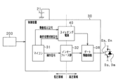
- FIG. 1 is a configuration diagram of a power supply system
- FIG. 2 is a block diagram of a control device
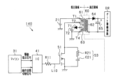
- FIG. 3 is a block diagram of a switching power supply
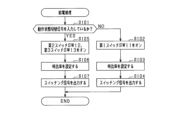
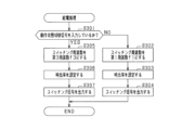
- FIG. 4 is a flowchart of a power supply process.
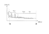
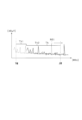
- FIG. 5 is a diagram showing the relationship between noise magnitude and frequency.
- FIG. 6 is a configuration diagram of a switching power supply according to a second embodiment
- FIG. 7 is a flowchart of a power supply process according to the second embodiment.
- FIG. 8 is a diagram showing the relationship between noise magnitude and frequency in the second embodiment
- FIG. 9 is a flowchart of a power supply process according to a third embodiment.
- FIG. 10 is a diagram showing the relationship between noise magnitude and frequency in the third embodiment.
- the insulated power supply device of this embodiment is mounted on the power supply system of a mobile body, including, for example, an electric vehicle or a hybrid vehicle.
- the power supply system 10 includes a motor 11 as a rotating electric machine, an inverter 12 as a power conversion device, a high-voltage battery 20 as a power storage device, and a control device 30.
- the motor 11 is connected to the inverter 12 and serves as a main engine of a mobile body.
- the inverter 12 is a three-phase inverter and is connected to the high-voltage battery 20.
- the control device 30 controls the motor 11 by controlling the inverter 12. A detailed description will be given below.
- Motor 11 is a three-phase synchronous machine, and includes star-connected U-, V-, and W-phase armature windings 11a-11c, and a rotor (not shown).
- the armature windings 11a-11c of each phase are arranged with an electrical angle of 120°.
- Motor 11 is, for example, a permanent magnet synchronous machine.
- the rotor is capable of transmitting power to, for example, the drive wheels of a mobile object. Motor 11 therefore serves as a source of torque that drives the mobile object.
- the inverter 12 is a three-phase full-bridge inverter having three phases of series connections (legs) of upper arm switches Sp and lower arm switches Sn, which are connected in parallel.
- An upper arm diode Dp which is a freewheel diode, is connected in inverse parallel (reverse polarity) to the upper arm switch Sp
- a lower arm diode Dn which is also a freewheel diode, is connected in inverse parallel to the lower arm switch Sn.
- each switch Sp, Sn is a semiconductor switch element (semiconductor device), and is, for example, an IGBT, but may also be a MOSFET.
- the upper arm switch Sp and the lower arm switch Sn may be collectively referred to as upper and lower arm switches Sp, Sn below.
- the inverter 12 is equipped with a smoothing capacitor 13.
- the high-potential terminal of the smoothing capacitor 13 is connected to the positive power supply path H1.
- the low-potential terminal of the smoothing capacitor 13 is connected to the negative power supply path L1.
- the smoothing capacitor 13 may be provided outside the inverter 12.
- the first ends of the armature windings 11a to 11c are connected to the connection point between the emitter, which is the low potential terminal of the upper arm switch Sp, and the collector, which is the high potential terminal of the lower arm switch Sn, via a conductive member 14 such as a bus bar.
- the second ends of the armature windings 11a to 11c of each phase are connected to each other at the neutral point.
- the collector of the upper arm switch Sp of each phase is connected to the positive power supply path H1.
- the emitter of the lower arm switch Sn of each phase is connected to the negative power supply path L1. This connects the inverter 12 to the high voltage battery 20 via the positive power supply path H1 and the negative power supply path L1.
- the positive power supply path H1 and the negative power supply path L1 are provided with a main switch SMR that switches between energizing and deenergizing the power supply paths H1 and L1.
- the main switch SMR is a mechanical relay switch, but may also be a semiconductor switch.
- the high-voltage battery 20 is a power supply source for driving the rotor of the motor 11 to rotate.
- the high-voltage battery 20 is a battery pack configured as a series connection of battery cells, which are single batteries.
- the positive terminal of the high-voltage battery 20 is connected to the positive power supply path H1, and the negative terminal is connected to the negative power supply path L1.
- the inter-terminal voltages (e.g., rated voltages) of the battery cells that make up the battery pack are set to be the same, for example.
- the battery cells are secondary batteries such as lithium-ion batteries.
- the power supply system 10 also includes an external charging mechanism 80 for connection to an external charger 100 as an external power supply.
- the external charging mechanism 80 includes an inlet 82 and a relay 81.
- the inlet 82 is connected to the power supply paths H1, L1 between the high-voltage battery 20 and the inverter 12 via the relay 81.
- the inlet 82 is configured to supply power from the external charger 100 to the high-voltage battery 20 during external charging when the main switch SMR and the relay 81 are in the on state (closed state, energized state). As shown in FIG. 1, the inlet 82 may be connected to the neutral point of the motor 11 to enable neutral point charging.
- the external charger 100 includes a connector 110 that is configured to be connectable to the inlet 82 of the vehicle.
- the external charger 100 is, for example, a DC power source, but may also be an AC power source. In this case, an AC/DC converter or the like is required in the external charger 100 or the power supply system 10.
- an AC/DC converter is provided in the power supply system 10
- some of the circuit elements that configure the motor 11 and the inverter 12 may be reused.
- the system may be configured so that charging power is supplied to the inverter 12 via the motor 11, the inverter 12 is operated, and the power is converted by the motor 11 and the inverter 12 to charge the high-voltage battery 20.
- the control device 30 is mainly composed of a microcontroller 31 (microcontroller unit) and is driven by power supplied from a low-voltage battery 21 as a DC power source.
- the microcontroller 31 has a CPU.
- the functions provided by the microcontroller 31 can be provided by software recorded in a physical memory device and a computer that executes the software, software only, hardware only, or a combination of these.
- a microcontroller when a microcontroller is provided by an electronic circuit, which is hardware, it can be provided by a digital circuit including a large number of logic circuits, or an analog circuit.
- a microcontroller executes a program stored in a non-transitory tangible storage medium serving as a memory unit that the microcontroller has. When a program is executed, a method corresponding to the program is performed.
- the memory unit is, for example, a non-volatile memory.
- the program stored in the memory unit can be updated via a communication network such as the Internet, for example, over the air (OTA).
- OTA over the air
- the microcomputer 31 operates the inverter 12 to control the torque of the motor 11 to the command torque Trq* based on the detection values of various sensors (not shown) (such as a voltage sensor, a current sensor, and a rotation angle sensor).
- the control device 30 generates an operation signal to turn on and off each of the switches Sp, Sn that make up the inverter 12, and outputs the operation signal to the gate drive circuit DR (drive circuit) of each switch Sp, Sn via the interface unit 32.
- the low-voltage battery 21 is a storage battery whose output voltage is lower than the output voltage of the high-voltage battery 20, for example a lead-acid battery. In this embodiment, the low-voltage battery 21 corresponds to the "DC power source.”
- the interface unit 32 has the function of transmitting signals between the high-voltage area including the motor 11, inverter 12, and high-voltage battery 20 and the low-voltage area including the control device 30 and low-voltage battery 21 while electrically insulating these systems.
- the interface unit 32 is, for example, a photocoupler.
- the switching power supply 40 has a function of supplying drive power to the gate drive circuit DR that drives each switch Sp, Sn while providing insulation between the high voltage region and the low voltage region.
- the switching power supply 40 is a flyback type switching power supply.
- the switching power supply 40 includes a power supply IC 41 and a control switch circuit 50.
- the power supply IC 41 and the control switch circuit 50 are provided in a low-voltage region.
- the power supply IC 41 controls the on/off of the control switch circuit 50 by a switching signal. Therefore, the power supply IC 41 is a switch control unit.
- the control switch circuit 50 When the control switch circuit 50 is turned on, it supplies power from the low-voltage battery 21 to each transformer 60, and when it is turned off, it stops the supply of power from the low-voltage battery 21 to each transformer 60.
- the configuration of the control switch circuit 50 will be described later.
- the switching power supply 40 includes a transformer 60 that supplies power to the gate drive circuits DR of the switches Sp and Sn.
- the transformer 60 may be provided for each gate drive circuit DR, or a part or all of the transformer 60 may be shared.
- the transformer 60 has an input winding 61 which is a primary winding, and an output winding 62 and a feedback winding 63 which are secondary windings.
- the transformer 60 has a common core around which the windings 61, 62, and 63 are wound, and the windings 61, 62, and 63 are magnetically coupled by the common core.
- the input winding 61 and the feedback winding 63 are provided in the low voltage region.
- the output winding 62 is provided in the high voltage region.
- the transformer 60 has a number of terminals.
- the output terminals of the transformer 60 are connected to corresponding output windings 62.
- the first terminal T1 of the transformer 60 is connected to the second terminal T2 of the transformer 60 via the input winding 61.
- the third terminal T3 of the transformer 60 is connected to the fourth terminal T4 of the transformer 60 via the feedback winding 63.
- the output terminal of the transformer 60 is connected to the gate drive circuit DR via an output diode 64 and an output capacitor 65.
- the first terminal T1 of the transformer 60 is connected to the positive terminal of the low-voltage battery 21 via a wire.
- the negative side of the low-voltage battery 21 is connected to ground.
- the second terminal T2 of the transformer 60 is connected to the control switch circuit 50 via a wire.
- the third terminal T3 of the transformer 60 is connected to the anode of the feedback diode 71.
- the cathode of the feedback diode 71 is connected to ground via a feedback capacitor 72.
- the fourth terminal T4 of the transformer 60 is connected to ground via a wiring.
- the control switch circuit 50 includes a control switch 51.
- the control switch 51 is a voltage-controlled semiconductor switch, specifically an N-channel MOSFET.
- the drain of the control switch 51 is connected to the second terminal T2 of the transformer 60.
- the source of the control switch 51 is connected to ground.
- This control switch 51 is connected to the power supply IC 41 via an electrical path L10, and a switching signal for controlling on/off switching can be input from the power supply IC 41 to the gate via the electrical path L10.
- this electrical path L10 is provided with a resistance circuit 52 for changing the switching speed when the switching signal switches from a high level state to a low level state or from a low level state to a high level state.
- This resistor circuit 52 is configured to be able to change its resistance value. More specifically, the resistor circuit 52 includes a first resistor R11 as a first resistor element, a first switch SW11 connected in series to the first resistor R11, a second resistor R12 as a second resistor element, and a second switch SW12 connected in series to the first resistor R11.
- the series connection of the first resistor R11 and the first switch SW11 is provided on the electrical path L10, and the series connection of the second resistor R12 and the second switch SW12 is connected in parallel to the series connection of the first resistor R11 and the first switch SW11.
- the resistance value of the first resistor R11 and the resistance value of the second resistor R12 are different, and specifically, the resistance value of the second resistor R12 is greater than the resistance value of the first resistor R11.
- the power supply IC 41 outputs a switching signal by turning on either the first switch SW11 or the second switch SW12. Therefore, when the second switch SW12 is turned on, it is possible to slow down the switching speed of the switching signal input to the control switch 51 compared to when the first switch SW11 is turned on.
- a snubber circuit 55 is connected in parallel to the control switch 51.
- the snubber circuit 55 is configured so that its time constant can be changed.
- the snubber circuit 55 is configured by connecting a first snubber circuit 53 and a second snubber circuit 54 in parallel.
- the first snubber circuit 53 and the second snubber circuit 54 are each an RC snubber circuit for absorbing the transient high voltage that occurs when the switch is turned off.
- the first snubber circuit 53 is composed of a series connection of a first snubber resistor R21 and a first snubber capacitor C21.
- the high potential side terminal of this first snubber circuit 53 (the terminal on the first snubber resistor R21 side) is connected to the high potential side terminal side (drain side) of the control switch 51.
- the low potential side terminal of this first snubber circuit 53 (the terminal on the first snubber capacitor C21 side) is connected to the low potential side terminal side (source side, i.e., ground) of the control switch 51.
- the second snubber circuit 54 is composed of a series connection of a second snubber resistor R22 and a second snubber capacitor C22.
- the high-potential terminal of this second snubber circuit 54 (the terminal on the second snubber resistor R22 side) is connected to the high-potential terminal (drain side) of the control switch 51.
- the low-potential terminal of this second snubber circuit 54 (the terminal on the second snubber capacitor C22 side) is connected to the low-potential terminal (source side, i.e., ground) of the control switch 51 via a third switch SW13 that serves as a snubber changeover switch.
- the third switch SW13 is connected in series to the second snubber circuit 54, and when the third switch SW13 is turned on, it is electrically connected to the control switch 51, and when it is turned off, it is disconnected.
- the power supply IC 41 is capable of controlling the on/off of this third switch SW13, and when the third switch SW13 is turned on, it is possible to make the time constant of the snubber circuit 55 larger and the switching speed slower than when the third switch SW13 is off.
- the resistance value of the first snubber resistor R21, the resistance value of the second snubber resistor R22, the capacitance of the first snubber capacitor C21, and the capacitance of the second snubber capacitor C22 may be set arbitrarily.
- the resistance value of the second snubber resistor R22 may be made larger than the resistance value of the first snubber resistor R21, and the capacitance of the second snubber capacitor C22 may be made larger than the capacitance of the first snubber capacitor C21.
- the power supply IC 41 is an integrated circuit, and the functions provided by the power supply IC 41, like the microcomputer 31, can be provided by software recorded in a physical memory device and a computer that executes the software, by software alone, by hardware alone, or a combination of these.
- the power supply IC 41 controls the on/off of the control switch circuit 50 according to a predetermined power supply control program. Specifically, the power supply IC 41 controls the on/off of the control switch circuit 50 to supply power from the low-voltage battery 21 to the gate drive circuit DR while electrically insulating the low-voltage battery 21 from the gate drive circuit DR.
- the power supply IC 41 sets a duty ratio Ton/Tsw where one switching period in the control switch circuit 50 is Tsw and the on-time is Ton. Then, a switching signal according to the set duty ratio is output to the control switch circuit 50.
- the power supply IC 41 corresponds to the "switch control unit.” When a switching signal is input to the control switch circuit 50, the on/off of the control switch 51 is controlled according to the switching signal input to its gate.
- the control switch 51 When the control switch 51 is turned on, power is supplied to the input winding 61 from the low-voltage battery 21. During this time, an induced voltage is generated in the feedback winding 63 such that the potential of the fourth terminal T4 of the transformer 60 becomes higher than the third terminal T3. In this case, the flow of current to the feedback winding 63 is restricted by the feedback diode 71, and magnetic energy is stored in the transformer 60. As in the case of the feedback winding 63, the flow of current to the output winding 62 is restricted by the output diode 64.
- the power supply system 10 is connected to an external charger 100 and is configured to be capable of external charging.
- external charging When external charging is performed, if the charging voltage of the external charger 100 is applied to the motor 11 as well as the high-voltage battery 20, a parasitic capacitance is generated in the motor 11, which may cause the motor 11 to operate unintentionally.
- the switching power supply 40 needs to supply drive power to the gate drive circuit DR for operating the upper and lower arm switches Sp, Sn during external charging.
- noise occurs due to switching. It is preferable to reduce such noise during external charging.
- a noise threshold Th is set for each frequency band, and laws and regulations require that noise not exceed the noise threshold Th.
- the switching power supply 40 of this embodiment executes the following process during external charging. This will be explained in detail below.
- a host control device 200 such as a host ECU or a battery control ECU notifies the control device 30 of this.
- the microcomputer 31 of the control device 30 outputs a drive instruction signal to the power supply IC 41 of the switching power supply 40.
- the host control device 200 notifies the control device 30 that external charging is in progress.
- the microcomputer 31 of the control device 30 outputs an operation state switching signal to the power supply IC 41. Therefore, the microcomputer 31 functions as a power supply control device.
- the power supply IC 41 When the power supply IC 41 receives a drive instruction signal, it performs the power supply process shown in FIG. 4 at predetermined intervals. First, the power supply IC 41 determines whether or not an operation state switching signal has been received, i.e., whether or not external charging is in progress (step S101). If the determination result is negative, the power supply IC 41 turns on the first switch SW11 and turns off the second and third switches SW12 and SW13 (step S102). The power supply IC 41 also sets the time ratio Ton/Tsw when one switching period in the control switch circuit 50 is Tsw and the on time is Ton (step S103).
- step S104 the power supply IC 41 outputs a switching signal according to the duty ratio set in step S103 to the control switch circuit 50 (step S104). This causes the switching signal to be input to the gate of the control switch 51, and the control switch 51 is turned on and off in accordance with the switching signal. Then, when the control switch 51 is turned on and off, as described above, drive power is supplied to the gate drive circuit DR.
- step S101 determines whether the determination result in step S101 is positive. If the determination result in step S101 is positive, the power supply IC 41 turns off the first switch SW11 and turns on the second and third switches SW12 and SW13 (step S105). The power supply IC 41 also sets the time ratio Ton/Tsw when one switching period in the control switch circuit 50 is Tsw and the on time is Ton (step S106).
- step S106 the power supply IC 41 outputs a switching signal according to the duty ratio set in step S106 to the control switch circuit 50 (step S107) while keeping the second and third switches SW12 and SW13 on.
- step S107 the control switch 51 is turned on and off, and drive power is supplied to the gate drive circuit DR.
- the second and third switches SW12 and SW13 are turned on and the power supply IC 41 outputs a switching signal.
- the resistance circuit 52 the second resistor R12, which has a larger resistance value than the first resistor R11, is switched to, and the resistance value of the resistance circuit 52 becomes larger than the normal value (the resistance value of the first resistor R11).
- the second snubber circuit 54 is also connected to the control switch 51, and the time constant of the snubber circuit 55 becomes larger than the normal value (the time constant of only the first snubber circuit 53). Therefore, the switching speed can be slowed down. As a result, the speed at which the control switch 51 switches from on to off or from off to on can be slowed down.
- FIG. 5 shows noise generated by the switching power supply 40 while it is in operation.
- the vertical axis shows the noise magnitude [dB ⁇ V], and the horizontal axis shows the noise frequency [MHz].
- FIG. 5 also shows the noise threshold Th determined by laws and regulations for each frequency band.
- the noise threshold Th is a threshold when the mobile object is stopped, that is, during external charging.
- the frequency range for which the noise threshold Th is set has upper and lower limits.
- the noise threshold Th differs for each frequency band. For example, the noise threshold Th1 in the low frequency band is larger than the noise threshold Th2 in the high frequency band. In other words, even larger noise is tolerated in the low frequency band compared to the high frequency band.
- the noise when the operation state switching signal is not input i.e., when external charging is not in progress
- the noise when the operation state switching signal is input i.e., when external charging is in progress
- the switching power supply 40 of the first embodiment suppresses the noise level overall by slowing down the switching speed. In other words, it is possible to reduce the noise level evenly across all frequency bands, and it is easy to reduce the noise level below the noise threshold Th.
- the power supply IC 41 switches the resistance value of the resistor circuit 52 to a predetermined normal value and inputs a switching signal to the control switch 51 to control on/off switching.
- the power supply IC 41 switches the resistance value of the resistor circuit 52 to a value greater than the normal value and inputs a switching signal to the control switch 51, thereby slowing down the switching speed. More specifically, in normal operation, the power supply IC 41 turns on the first switch SW11 and inputs a switching signal to the control switch 51 via the first resistor R11.
- the power supply IC 41 turns on the second switch SW12 and inputs a switching signal via the second resistor R12. This makes it possible to slow down the switching speed with a simple circuit configuration.
- the power supply IC 41 normally switches the time constant in the snubber circuit 55 to a predetermined normal value and inputs a switching signal to the control switch 51 to control on/off switching.
- the power supply IC 41 switches the time constant in the snubber circuit 55 to a value larger than the normal value and inputs a switching signal to the control switch 51. That is, the power supply IC 41 normally inputs a switching signal to the control switch 51 with the first snubber circuit 53 connected in parallel to the control switch 51.
- the power supply IC 41 inputs a switching signal with the first snubber circuit 53 and the second snubber circuit 54 connected in parallel to the control switch 51. This makes it possible to slow down the switching speed with a simple circuit configuration.
- the switching power supply 140 of the second embodiment does not have a configuration for slowing down the switching speed, specifically, the second resistor R12 and the second snubber circuit 54. That is, as shown in FIG. 6, the power supply IC 41 is connected to the gate of the control switch 51 via the first resistor R11, but does not have the second resistor R12 and cannot be switched. In addition, only the first snubber circuit 53 is connected in parallel to the control switch 51, and the second snubber circuit 54 is not added and connected in parallel.
- the power supply IC 41 is configured to be able to change the switching frequency. More specifically, when the power supply IC 41 of the second embodiment receives a drive instruction signal, it performs the power supply process shown in FIG. 7 at predetermined intervals. First, the power supply IC 41 determines whether or not an operation state switching signal has been received (step S201). If the determination result is negative, the power supply IC 41 sets the switching frequency (operating frequency) to a predetermined first frequency f1 (step S202). Then, the power supply IC 41 identifies the switching period Tsw1 from the first frequency f1 and sets the duty ratio Ton1/Tsw1 (step S203).
- the power supply IC 41 outputs a switching signal according to the duty ratio set in step S203 to the control switch circuit 50 (step S204).
- the switching signal is operated at the switching frequency (first frequency f1) set in step S202.
- the switching signal is input to the gate of the control switch 51, and the control switch 51 is turned on and off in accordance with the switching signal.
- driving power is supplied to the gate drive circuit DR.
- step S201 determines whether the determination result in step S201 is positive. If the determination result in step S201 is positive, the power supply IC 41 sets the switching frequency to a second frequency f2 different from the first frequency f1 (step S205). The second frequency f2 is a lower frequency than the first frequency f1. The power supply IC 41 then identifies the switching period Tsw2 from the second frequency f2 and sets the duty ratio Ton2/Tsw2 (step S206). The power supply IC 41 then outputs a switching signal according to the duty ratio set in step S206 to the control switch circuit 50 (step S207). At this time, the switching signal is operated at the switching frequency (second frequency f2) set in step S205. This turns the control switch 51 on and off, and driving power is supplied to the gate drive circuit DR.
- FIG. 8 shows noise based on the operation of the switching power supply 140 of the second embodiment.
- the frequency range for which the noise threshold Th is set has upper and lower limits.
- the noise threshold Th differs for each frequency band. For example, the noise threshold Th1 in the low frequency band is larger than the noise threshold Th2 in the high frequency band. In other words, even larger noise is tolerated in the low frequency band compared to the high frequency band.
- the power supply IC 41 of the second embodiment therefore sets the switching frequency to a second frequency f2 during external charging, which is lower than the first frequency f1 during normal operation. That is, the power supply IC 41 lowers the switching frequency (operating frequency) during external charging, shifting the noise frequency overall to the lower frequency side (left side). This makes it possible to move noise that was in the high frequency band to a low frequency band and make it below the noise threshold Th. Alternatively, it moves the noise to a low frequency band where no noise threshold Th is set (a frequency band lower than the lower limit of the threshold Th), thereby satisfying the noise requirements.
- the switching speed is not slowed down, so heat generation that accompanies a decrease in switching speed is suppressed, and power consumption can be reduced.
- the circuit configuration of the switching power supply 140 of the third embodiment is the same as that of the second embodiment (see FIG. 6), so its description will be omitted. And, like the second embodiment, the power supply IC 41 of the third embodiment is configured to be able to change the switching frequency.
- the power supply IC 41 of the third embodiment performs the power supply process shown in FIG. 9 at predetermined intervals.
- the processes of steps S301 to S304 are the same as steps S201 to S204, and therefore will be omitted.
- the power supply IC 41 sets the switching frequency to a third frequency f3 different from the first frequency f1 (step S305).
- the third frequency f3 is a higher frequency than the first frequency f1.
- the power supply IC 41 identifies the switching period Tsw3 from the third frequency f3 and sets the duty ratio Ton3/Tsw3 (step S306).
- the power supply IC 41 then outputs a switching signal according to the duty ratio set in step S306 to the control switch circuit 50 (step S307). At this time, the switching signal is operated at the switching frequency (third frequency f3) set in step S305. This turns the control switch 51 on and off, and driving power is supplied to the gate drive circuit DR.
- Fig. 10 shows noise based on the operation of the switching power supply 40 of the second embodiment.
- the power supply IC 41 of the third embodiment sets the switching frequency to a third frequency f3 that is higher than the first frequency f1 during normal operation during external charging. That is, the power supply IC 41 of the third embodiment increases the switching frequency (operating frequency) during external charging, shifting the noise frequency overall to the higher frequency side (right side). At that time, the noise Ns1 that exceeds the noise threshold Th during normal operation is shifted so that it falls outside the upper limit of the frequency range in which the noise threshold Th is set. This satisfies the noise requirements.
- the switching speed is not slowed down, so heat generation that accompanies a decrease in switching speed is suppressed, and power consumption can be reduced.
- the power supply IC 41 may input a current value from the feedback winding 63 and perform feedback control based on the current value.
- the feedback winding 63 does not need to be provided.
- the first and second embodiments may be combined. That is, the power supply IC 41 may turn on the second and third switches SW12 and SW13 to slow down the switching speed and lower the switching frequency (operating frequency).
- the first and third embodiments may be combined. That is, the power supply IC 41 may turn on the second and third switches SW12 and SW13 to slow down the switching speed and increase the switching frequency.
- only one of the second resistor R12 and the second snubber circuit 54 may be provided.
- the switching speed can be slowed down by using only one of them.
- the switching speed is slowed down by switching to the second resistor R12, but the circuit configuration of the resistor circuit 52 may be changed as desired if the resistance value is changeable.
- the switching speed is slowed down by connecting the second snubber circuit 54, but the circuit configuration of the snubber circuit 55 may be changed as desired if the time constant can be changed.
- control unit and the method described in the present disclosure may be realized by a dedicated computer provided by configuring a processor and memory programmed to execute one or more functions embodied in a computer program.
- control unit and the method described in the present disclosure may be realized by a dedicated computer provided by configuring a processor with one or more dedicated hardware logic circuits.
- control unit and the method described in the present disclosure may be realized by one or more dedicated computers configured by combining a processor and memory programmed to execute one or more functions with a processor configured with one or more hardware logic circuits.
- the computer program may be stored in a computer-readable non-transient tangible recording medium as instructions executed by the computer.
- the control switch circuit includes: A control switch (51) connected to the primary winding and switching between supplying power to the primary winding and stopping the supply of power thereto; a resistor circuit (52) provided in an electrical path between the gate of the control switch and the switch control unit, the resistor circuit is configured so that its resistance value can be changed;
- the switch control unit is During normal operation when the operation state switching signal is not input, the resistance value of the resistor circuit is switched to a predetermined normal value, and a switching signal for controlling on/off switching is input to the control switch. 2.
- the isolated power supply device wherein, when the operation state switching signal is input, a resistance value in the resistor circuit is switched to a value larger than the normal value, and the switching speed is slowed down by inputting the switching signal to the control switch.
- the control switch circuit includes: A control switch (51) connected to the primary winding and switching between supplying power to the primary winding and stopping the supply of power thereto; a snubber circuit (55) configured with a series connection of a capacitor and a resistor and connected in parallel to the control switch; The snubber circuit is configured so that its time constant can be changed, The switch control unit is During normal operation when the operation state switching signal is not input, a time constant in the snubber circuit is switched to a predetermined normal value, and a switching signal for controlling on/off switching is input to the control switch, 3.
- the isolated power supply device is mounted on a power supply system (10) capable of performing external charging for charging an electricity storage device (20) from an external power supply (100), the semiconductor device is a semiconductor switching element constituting an inverter (12) that converts electric power from the power storage device and supplies the electric power to a motor; the drive circuit is a gate drive circuit that inputs an operation signal to a gate of the semiconductor switching element of the inverter, 4.
- the isolated power supply device according to any one of configurations 1 to 3, wherein the operation state switching signal is input to the switch control unit during external charging.
- the inverter is provided in a power supply path between the motor (11) and the power storage device, 5.
- the isolated power supply device according to configuration 4, wherein during external charging, the semiconductor switching element of the inverter is turned on and off, so that power of the external power supply is converted by the motor and the inverter and supplied to the power storage device.
- a power supply system (10) capable of performing external charging for charging an electricity storage device (20) from an external power supply (100), comprising: an inverter (12) provided in a power supply path between a motor (11) and the electricity storage device; A drive circuit (DR) for semiconductor switching elements (Sp, Sn) constituting the inverter; an isolated power supply device (40) for supplying power to the drive circuit; A power supply control device (31) that controls the insulated power supply device, The isolated power supply device comprises: A primary winding (61) connected to a DC power source (21); a secondary winding (62) capable of being magnetically coupled to the primary winding via a core; a control switch circuit (50) that, when turned on, supplies power from the DC power source to the primary winding and, when turned off, stops the supply of power from the DC power source to the primary winding; A switch control unit (41) that controls the on/off of the control switch circuit, During external charging, the semiconductor switching element of the inverter is turned on and off, whereby power from the external power supply (100
- the isolated power supply device comprises: A primary winding (61) connected to a DC power source; a secondary winding (62) capable of being magnetically coupled to the primary winding via a core; a control switch circuit (50) that, when turned on, supplies power from the DC power source to the primary winding and, when turned off, stops the supply of power from the DC power source to the primary winding;
- a switch control unit (41) that controls the on/off of the control switch circuit, a power supply control program that, when an operating state switching signal is input to the isolated power supply device, causes the switch control unit to perform on/off control by making a switching frequency different from that in normal times and by making the switching speed slower than that in normal times, or by executing either one of these.
Landscapes
- Engineering & Computer Science (AREA)
- Power Engineering (AREA)
- Dc-Dc Converters (AREA)
Applications Claiming Priority (2)
| Application Number | Priority Date | Filing Date | Title |
|---|---|---|---|
| JP2023063752A JP7848738B2 (ja) | 2023-04-10 | 2023-04-10 | 絶縁型電源装置、電源システム、及び電源制御プログラム |
| JP2023-063752 | 2023-04-10 |
Publications (1)
| Publication Number | Publication Date |
|---|---|
| WO2024214506A1 true WO2024214506A1 (ja) | 2024-10-17 |
Family
ID=93059165
Family Applications (1)
| Application Number | Title | Priority Date | Filing Date |
|---|---|---|---|
| PCT/JP2024/010970 Ceased WO2024214506A1 (ja) | 2023-04-10 | 2024-03-21 | 絶縁型電源装置、電源システム、及び電源制御プログラム |
Country Status (2)
| Country | Link |
|---|---|
| JP (1) | JP7848738B2 (https=) |
| WO (1) | WO2024214506A1 (https=) |
Citations (5)
| Publication number | Priority date | Publication date | Assignee | Title |
|---|---|---|---|---|
| JP2019201532A (ja) * | 2018-05-18 | 2019-11-21 | 株式会社デンソー | インバータ制御システム |
| JP2020031462A (ja) * | 2018-08-21 | 2020-02-27 | キヤノン株式会社 | スイッチング電源 |
| JP2020145850A (ja) * | 2019-03-06 | 2020-09-10 | トヨタ自動車株式会社 | 車両用電源システム |
| WO2021230177A1 (ja) * | 2020-05-15 | 2021-11-18 | 株式会社デンソー | 電力変換器の制御回路 |
| JP2022118417A (ja) * | 2021-02-02 | 2022-08-15 | トヨタ自動車株式会社 | 電源システム |
-
2023
- 2023-04-10 JP JP2023063752A patent/JP7848738B2/ja active Active
-
2024
- 2024-03-21 WO PCT/JP2024/010970 patent/WO2024214506A1/ja not_active Ceased
Patent Citations (5)
| Publication number | Priority date | Publication date | Assignee | Title |
|---|---|---|---|---|
| JP2019201532A (ja) * | 2018-05-18 | 2019-11-21 | 株式会社デンソー | インバータ制御システム |
| JP2020031462A (ja) * | 2018-08-21 | 2020-02-27 | キヤノン株式会社 | スイッチング電源 |
| JP2020145850A (ja) * | 2019-03-06 | 2020-09-10 | トヨタ自動車株式会社 | 車両用電源システム |
| WO2021230177A1 (ja) * | 2020-05-15 | 2021-11-18 | 株式会社デンソー | 電力変換器の制御回路 |
| JP2022118417A (ja) * | 2021-02-02 | 2022-08-15 | トヨタ自動車株式会社 | 電源システム |
Also Published As
| Publication number | Publication date |
|---|---|
| JP7848738B2 (ja) | 2026-04-21 |
| JP2024150357A (ja) | 2024-10-23 |
Similar Documents
| Publication | Publication Date | Title |
|---|---|---|
| JP6418252B2 (ja) | 回転電機制御装置 | |
| JP6668930B2 (ja) | 電力変換装置および電動車両の制御装置 | |
| CN106165277B (zh) | 逆变器控制装置 | |
| CN106104998B (zh) | 逆变器控制装置 | |
| JP6291899B2 (ja) | 回転電機制御装置 | |
| JP6253850B2 (ja) | 交流回転電機の制御装置 | |
| JP7259563B2 (ja) | 回転電機制御システム | |
| JP2022177342A (ja) | 電力変換装置 | |
| JP7243676B2 (ja) | 電力変換器の制御回路 | |
| JP7790585B2 (ja) | 電力変換装置、プログラム及び制御方法 | |
| JP2020058178A (ja) | 充電制御方法および充電制御装置 | |
| JP6307983B2 (ja) | インバータ制御装置 | |
| JP2017118806A (ja) | 電力変換装置および制御方法 | |
| JP2021129396A (ja) | 電力変換器の制御回路 | |
| JP6079455B2 (ja) | 充電装置及び制御方法 | |
| JP7718601B2 (ja) | 電力変換装置、プログラム | |
| JP7848738B2 (ja) | 絶縁型電源装置、電源システム、及び電源制御プログラム | |
| JP7354958B2 (ja) | 電力変換器の制御回路 | |
| JP2014155308A (ja) | 充電装置 | |
| WO2018207829A1 (ja) | 回転電機装置の制御装置 | |
| JP7669901B2 (ja) | 電力変換装置 | |
| JP7810147B2 (ja) | 電源装置、電源制御装置、及び電源制御プログラム | |
| JP2025049820A (ja) | 電力変換装置及びプログラム | |
| WO2024224950A1 (ja) | 電源システム及び電源制御プログラム | |
| WO2025177794A1 (ja) | 電力変換装置 |
Legal Events
| Date | Code | Title | Description |
|---|---|---|---|
| 121 | Ep: the epo has been informed by wipo that ep was designated in this application |
Ref document number: 24788536 Country of ref document: EP Kind code of ref document: A1 |
|
| NENP | Non-entry into the national phase |
Ref country code: DE |
|
| 122 | Ep: pct application non-entry in european phase |
Ref document number: 24788536 Country of ref document: EP Kind code of ref document: A1 |