WO2024209586A1 - 光源ユニット、照明ユニット、露光装置、及び露光方法 - Google Patents
光源ユニット、照明ユニット、露光装置、及び露光方法 Download PDFInfo
- Publication number
- WO2024209586A1 WO2024209586A1 PCT/JP2023/014075 JP2023014075W WO2024209586A1 WO 2024209586 A1 WO2024209586 A1 WO 2024209586A1 JP 2023014075 W JP2023014075 W JP 2023014075W WO 2024209586 A1 WO2024209586 A1 WO 2024209586A1
- Authority
- WO
- WIPO (PCT)
- Prior art keywords
- light source
- heat sink
- source unit
- unit according
- light
- Prior art date
- Legal status (The legal status is an assumption and is not a legal conclusion. Google has not performed a legal analysis and makes no representation as to the accuracy of the status listed.)
- Ceased
Links
Images


Classifications
-
- G—PHYSICS
- G03—PHOTOGRAPHY; CINEMATOGRAPHY; ANALOGOUS TECHNIQUES USING WAVES OTHER THAN OPTICAL WAVES; ELECTROGRAPHY; HOLOGRAPHY
- G03F—PHOTOMECHANICAL PRODUCTION OF TEXTURED OR PATTERNED SURFACES, e.g. FOR PRINTING, FOR PROCESSING OF SEMICONDUCTOR DEVICES; MATERIALS THEREFOR; ORIGINALS THEREFOR; APPARATUS SPECIALLY ADAPTED THEREFOR
- G03F7/00—Photomechanical, e.g. photolithographic, production of textured or patterned surfaces, e.g. printing surfaces; Materials therefor, e.g. comprising photoresists; Apparatus specially adapted therefor
- G03F7/70—Microphotolithographic exposure; Apparatus therefor
- G03F7/708—Construction of apparatus, e.g. environment aspects, hygiene aspects or materials
- G03F7/70858—Environment aspects, e.g. pressure of beam-path gas, temperature
- G03F7/70883—Environment aspects, e.g. pressure of beam-path gas, temperature of optical system
- G03F7/70891—Temperature
-
- G—PHYSICS
- G03—PHOTOGRAPHY; CINEMATOGRAPHY; ANALOGOUS TECHNIQUES USING WAVES OTHER THAN OPTICAL WAVES; ELECTROGRAPHY; HOLOGRAPHY
- G03F—PHOTOMECHANICAL PRODUCTION OF TEXTURED OR PATTERNED SURFACES, e.g. FOR PRINTING, FOR PROCESSING OF SEMICONDUCTOR DEVICES; MATERIALS THEREFOR; ORIGINALS THEREFOR; APPARATUS SPECIALLY ADAPTED THEREFOR
- G03F7/00—Photomechanical, e.g. photolithographic, production of textured or patterned surfaces, e.g. printing surfaces; Materials therefor, e.g. comprising photoresists; Apparatus specially adapted therefor
- G03F7/20—Exposure; Apparatus therefor
-
- G—PHYSICS
- G03—PHOTOGRAPHY; CINEMATOGRAPHY; ANALOGOUS TECHNIQUES USING WAVES OTHER THAN OPTICAL WAVES; ELECTROGRAPHY; HOLOGRAPHY
- G03F—PHOTOMECHANICAL PRODUCTION OF TEXTURED OR PATTERNED SURFACES, e.g. FOR PRINTING, FOR PROCESSING OF SEMICONDUCTOR DEVICES; MATERIALS THEREFOR; ORIGINALS THEREFOR; APPARATUS SPECIALLY ADAPTED THEREFOR
- G03F7/00—Photomechanical, e.g. photolithographic, production of textured or patterned surfaces, e.g. printing surfaces; Materials therefor, e.g. comprising photoresists; Apparatus specially adapted therefor
- G03F7/70—Microphotolithographic exposure; Apparatus therefor
- G03F7/70008—Production of exposure light, i.e. light sources
- G03F7/7005—Production of exposure light, i.e. light sources by multiple sources, e.g. light-emitting diodes [LED] or light source arrays
-
- G—PHYSICS
- G03—PHOTOGRAPHY; CINEMATOGRAPHY; ANALOGOUS TECHNIQUES USING WAVES OTHER THAN OPTICAL WAVES; ELECTROGRAPHY; HOLOGRAPHY
- G03F—PHOTOMECHANICAL PRODUCTION OF TEXTURED OR PATTERNED SURFACES, e.g. FOR PRINTING, FOR PROCESSING OF SEMICONDUCTOR DEVICES; MATERIALS THEREFOR; ORIGINALS THEREFOR; APPARATUS SPECIALLY ADAPTED THEREFOR
- G03F7/00—Photomechanical, e.g. photolithographic, production of textured or patterned surfaces, e.g. printing surfaces; Materials therefor, e.g. comprising photoresists; Apparatus specially adapted therefor
- G03F7/70—Microphotolithographic exposure; Apparatus therefor
- G03F7/70058—Mask illumination systems
- G03F7/70075—Homogenization of illumination intensity in the mask plane by using an integrator, e.g. fly's eye lens, facet mirror or glass rod, by using a diffusing optical element or by beam deflection
-
- H—ELECTRICITY
- H10—SEMICONDUCTOR DEVICES; ELECTRIC SOLID-STATE DEVICES NOT OTHERWISE PROVIDED FOR
- H10H—INORGANIC LIGHT-EMITTING SEMICONDUCTOR DEVICES HAVING POTENTIAL BARRIERS
- H10H20/00—Individual inorganic light-emitting semiconductor devices having potential barriers, e.g. light-emitting diodes [LED]
- H10H20/80—Constructional details
- H10H20/85—Packages
- H10H20/858—Means for heat extraction or cooling
-
- H—ELECTRICITY
- H10—SEMICONDUCTOR DEVICES; ELECTRIC SOLID-STATE DEVICES NOT OTHERWISE PROVIDED FOR
- H10H—INORGANIC LIGHT-EMITTING SEMICONDUCTOR DEVICES HAVING POTENTIAL BARRIERS
- H10H29/00—Integrated devices, or assemblies of multiple devices, comprising at least one light-emitting semiconductor element covered by group H10H20/00
- H10H29/80—Constructional details
- H10H29/85—Packages
- H10H29/858—Means for heat extraction or cooling
- H10H29/8582—Means for heat extraction or cooling characterised by their shape
-
- H—ELECTRICITY
- H10—SEMICONDUCTOR DEVICES; ELECTRIC SOLID-STATE DEVICES NOT OTHERWISE PROVIDED FOR
- H10H—INORGANIC LIGHT-EMITTING SEMICONDUCTOR DEVICES HAVING POTENTIAL BARRIERS
- H10H29/00—Integrated devices, or assemblies of multiple devices, comprising at least one light-emitting semiconductor element covered by group H10H20/00
- H10H29/80—Constructional details
- H10H29/85—Packages
- H10H29/858—Means for heat extraction or cooling
- H10H29/8586—Means for heat extraction or cooling comprising fluids, e.g. heat-pipes
Definitions
- liquid crystal display panels have come into widespread use as display elements for personal computers, televisions, and other devices.
- Liquid crystal display panels are manufactured by forming a circuit pattern of thin-film transistors on a plate (glass substrate) using photolithography techniques.
- An exposure device is used for this photolithography process, which projects and exposes the original pattern formed on a mask onto a photoresist layer on the plate via a projection optical system.
- the light source unit comprises a heat sink and a plurality of light source elements arranged two-dimensionally on a first surface of the heat sink, and the first surface of the heat sink is formed with a plurality of protrusions that protrude from the first surface and overlap at least one of the plurality of light source elements in a plan view.
- the exposure apparatus includes the above-mentioned illumination unit and a projection optical system that projects a pattern image of a mask illuminated by the illumination unit onto a photosensitive substrate.
- an exposure method is an exposure method using the above-mentioned exposure apparatus, and includes illuminating a mask with the illumination unit, and projecting a pattern image of the mask onto a photosensitive substrate using the projection optical system.
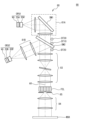
- FIG. 9A is a plan view illustrating a heat sink according to a first modified example of the second embodiment, and FIG. 9B is a cross-sectional view taken along line AA of FIG. 9A.
- FIG. 10A is a plan view illustrating a heat sink according to Modification 2 of the second embodiment, and FIG. 10B is a cross-sectional view taken along line AA of FIG. 10A.
- FIG. 11 is a cross-sectional view illustrating a heat sink according to the third embodiment.
- FIG. 12 is a diagram showing a preferable configuration of a lighting unit when using a heat sink according to the third embodiment.
- the exposure apparatus 10 is a scanning stepper (scanner) that transfers a pattern formed on the mask MSK onto a glass substrate (hereafter referred to as "plate") P by driving the mask MSK and the glass substrate P in the same direction and at the same speed relative to the projection optical system PL.
- the plate P is a rectangular glass substrate used, for example, in liquid crystal display devices (flat panel displays), with at least one side or diagonal length of 500 mm or more.
- the direction in which the mask MSK and plate P are driven during scanning exposure is defined as the X-axis direction
- the direction perpendicular to this in the horizontal plane is defined as the Y-axis direction
- the direction perpendicular to the X-axis and Y-axis is defined as the Z-axis direction
- the directions of rotation (tilt) around the X-axis, Y-axis, and Z-axis are defined as the ⁇ x, ⁇ y, and ⁇ z directions, respectively.
- the exposure apparatus 10 includes an illumination system IOP, a mask stage MST that holds a mask MSK, a projection optical system PL, a body 70 that supports these, a substrate stage PST that holds a plate P, and a control system for these.
- the control system provides overall control of each component of the exposure apparatus 10.
- the body 70 comprises a base (vibration isolation table) 71, columns 72A and 72B, an optical base 73, a support 74, and a slide guide 75.
- the base (vibration isolation table) 71 is placed on a floor F and supports the columns 72A, 72B, etc. by isolating vibrations from the floor F.
- the columns 72A and 72B each have a frame shape, and the column 72A is placed inside the column 72B.
- the optical base 73 has a flat plate shape and is fixed to the ceiling of the column 72A.
- the support 74 is supported by the ceiling of the column 72B via a slide guide 75.
- the slide guide 75 comprises an air ball lifter and a positioning mechanism, and positions the support 74 (i.e., the mask stage MST described later) at an appropriate position in the X-axis direction relative to the optical base 73.
- the illumination system IOP is disposed above the body 70.
- the illumination system IOP irradiates the mask MSK with illumination light IL.
- the detailed configuration of the illumination system IOP will be described later.
- the mask stage MST is supported by a support 74.
- a mask MSK having a pattern surface (the lower surface in FIG. 1) on which a circuit pattern is formed is fixed to the mask stage MST by, for example, vacuum adsorption (or electrostatic adsorption).
- the mask stage MST is driven by a drive system including, for example, a linear motor at a predetermined stroke in the scanning direction (X-axis direction) and is also slightly driven in the non-scanning directions (Y-axis direction and ⁇ z direction).
- the position information of the mask stage MST in the XY plane is measured by an interferometer system.
- the interferometer system measures the position of the mask stage MST by irradiating a measurement beam onto a movable mirror (or a mirror-finished reflective surface (not shown)) provided at the end of the mask stage MST and receiving the reflected light from the movable mirror.
- the measurement results are supplied to a control device (not shown), which drives the mask stage MST via a drive system in accordance with the measurement results of the interferometer system.
- the projection optical system PL is supported by the optical base 73 below (-Z side) the mask stage MST.
- the projection optical system PL is configured in the same manner as the projection optical system disclosed in, for example, US Pat. No. 5,729,331, and includes a plurality of (for example, seven) projection optical units 100 (multi-lens projection optical units) arranged in a staggered pattern, for example, to form a rectangular image field with the Y-axis direction as the longitudinal direction.
- four projection optical units 100 are arranged at a predetermined interval in the Y-axis direction, and the remaining three projection optical units 100 are arranged at a predetermined interval in the Y-axis direction, spaced apart from the four projection optical units 100 on the +X side.
- each of the multiple projection optical units 100 for example, a system that forms an erect normal image with a two-sided telecentric equal magnification system is used.
- the multiple projection areas of the projection optical units 100 arranged in a staggered pattern are collectively called the exposure area.
- the illumination light IL that has passed through the mask MSK forms a projected image (partial upright image) of the circuit pattern of the mask MSK in the illumination area in the irradiation area (exposure area (conjugate to the illumination area)) on the plate P arranged on the image plane side of the projection optical system PL via the projection optical system PL.
- a resist sensitizer
- the mask stage MST and the substrate stage PST By synchronously driving the mask stage MST and the substrate stage PST, i.e., by driving the mask MSK in the scanning direction (X-axis direction) relative to the illumination area (illumination light IL) and driving the plate P in the same scanning direction relative to the exposure area (illumination light IL), the plate P is exposed and the pattern of the mask MSK is transferred onto the plate P.
- the substrate stage PST is placed on a base (vibration isolation table) 71 below (on the -Z side) the projection optical system PL.
- a plate P is held on the substrate stage PST via a substrate holder (not shown).
- the position information of the substrate stage PST in the XY plane (including rotation information (yawing amount (amount of rotation in the ⁇ z direction ⁇ z), pitching amount (amount of rotation in the ⁇ x direction ⁇ x), and rolling amount (amount of rotation in the ⁇ y direction ⁇ y))) is measured by an interferometer system.
- the interferometer system measures the position of the substrate stage PST by irradiating a measurement beam from the optical base 73 to a movable mirror (or a mirror-finished reflective surface (not shown)) provided at the end of the substrate stage PST and receiving the reflected light from the movable mirror.
- the measurement result is supplied to a control device (not shown), which drives the substrate stage PST in accordance with the measurement result of the interferometer system.
- alignment measurement (e.g., EGA, etc.) is performed prior to exposure, and the plate P is exposed using the results in the following procedure.
- the mask stage MST and substrate stage PST are synchronously driven in the X-axis direction according to instructions from the control device. This performs scanning exposure on the first shot area on the plate P.
- the control device moves (steps) the substrate stage PST to a position corresponding to the second shot area. Then, scanning exposure is performed on the second shot area.
- the control device similarly repeats stepping between the shot areas of the plate P and scanning exposure on the shot areas to transfer the pattern of the mask MSK to all shot areas on the plate P.
- the illumination system IOP includes a plurality of illumination units 90 corresponding to the plurality of projection optical units 100 included in the projection optical system PL.
- FIG. 2 is a diagram showing a schematic configuration of the illumination unit 90.
- the illumination unit 90 includes a first light source unit OPU1, a second light source unit OPU2, and an illumination optical system 80.
- the first light source unit OPU1 includes a heat sink 40, a first light source array 20A, and a first magnifying optical system 30A
- the second light source unit OPU2 includes a heat sink 40, a second light source array 20B, and a second magnifying optical system 30B.
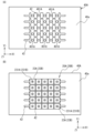
- FIG. 3(A) is a plan view showing a schematic configuration of the heat sink 40
- FIG. 3(B) is a cross-sectional view taken along line A-A in FIG. 3(A).
- the heat sink 40 has a rectangular planar shape.
- the longitudinal direction of the heat sink 40 is defined as the X1 direction, the lateral direction as the Y1 direction, and the thickness direction as the Z1 direction.
- the X1 direction, Y1 direction, and Z1 direction are mutually perpendicular.
- the heat sink 40 is made of a metal, such as copper, and is a microchannel heat sink with a thickness of 7 mm or less.
- the heat sink 40 has a flow path 402 through which the refrigerant passes, a refrigerant inlet 403 that supplies the refrigerant to the flow path 402, and a refrigerant outlet 404 that discharges the refrigerant that has passed through the flow path 402.
- the flow path 402 is shown by a dotted line.
- the flow path 402 meanders inside the heat sink 40.
- the heat sink 40 has a first surface 40a and a second surface 40b facing each other, and a plurality of protrusions 401 are formed on the first surface 40a, protruding from the first surface 40a and extending in the Y1 direction.
- each protrusion 401 is made of a part of the heat sink 40. That is, the protrusions 401 are made of a metal such as copper.
- the protrusions 401 can be formed, for example, by etching the first surface 40a of the heat sink 40 using a resist patterned by a photolithography process as a mask.
- the protrusions 401 may also be formed by machining the first surface 40a of the heat sink 40.
- An insulating layer 41 and a wiring layer 42 are formed in this order on the first surface 40a on both sides of each protrusion 401 in the X1 direction.
- FIG. 4(A) is a plan view that shows the state in which the first light source array 20A and the second light source array 20B are mounted on the heat sink 40
- FIG. 4(B) is a cross-sectional view taken along line A-A in FIG. 4(A)
- FIG. 4(C) is an enlarged view of the area surrounded by a circle C1 in FIG. 4(B). Note that hatching of the LED chips 23A and 23B, which will be described later, has been omitted in FIG. 4(B) and FIG. 4(C).
- the first light source array 20A has a plurality of LED (Light Emitting Diode) chips 23A (5 ⁇ 5 in FIG. 4(A)) arranged two-dimensionally on the first surface 40a of the heat sink 40.
- the number of LED chips 23A may be changed as necessary.
- Each LED chip 23A is arranged so as to overlap one of the multiple protrusions 401 in a planar view.
- each protrusion 401 overlaps with at least one of the multiple LED chips 23A in a planar view.
- each LED chip 23A is connected to the wiring layer 42 via solder 44.
- the LED chips 23A adjacent to each other in the X1 direction are connected in series by the wiring layer 42, and as shown by the arrow AR1 in FIG. 4(B), a current flows, for example, in the -X1 direction through the wiring layer 42 and the LED chip 23A.
- the LED chips 23A are arranged at a pitch P1, which is the distance between the centers of adjacent LED chips 23A.
- Each of the multiple LED chips 23A has a light-emitting portion 231A, and the peak wavelength of the light emitted from the light-emitting portion 231A is in the range of 380 to 390 nm.
- the light-emitting portion 231A is an ultraviolet LED (UV LED). It is more preferable that the peak wavelength of the light emitted from the light-emitting portion 231A is 385 nm.
- the light-emitting surface of the light-emitting portion 231A is square, and the length of one side is a1.
- the Z1 direction is approximately parallel to the optical axis of the light emitted by the light-emitting portion 231A.
- the second light source array 20B includes a plurality of LED chips 23B (5 x 5 in FIG. 4(A)) arranged two-dimensionally on the first surface 40a of the heat sink 40.
- the number of LED chips 23B may be changed as necessary.
- Each LED chip 23B is arranged so as to overlap one of the multiple protrusions 401 in a planar view. In other words, each protrusion 401 overlaps with at least one of the multiple LED chips 23B in a planar view.
- each LED chip 23B is connected to the wiring layer 42 via solder 44.
- the LED chips 23B adjacent to each other in the X1 direction are connected in series by the wiring layer 42, and as shown by the arrow AR1 in FIG. 4(B), a current flows, for example, in the -X1 direction through the wiring layer 42 and the LED chips 23B.
- the LED chips 23B are arranged at a pitch P2, which is the distance between the centers of adjacent LED chips 23B.
- the arrangement pitch P1 of the LED chips 23A and the arrangement pitch P2 of the LED chips 23B may be the same or different.
- Each of the multiple LED chips 23B has a light-emitting portion 231B, and the peak wavelength of the light emitted from the light-emitting portion 231B is in the range of 360 to 370 nm.
- the light-emitting portion 231B is a UV LED. It is more preferable that the peak wavelength of the light emitted from the light-emitting portion 231B is 365 nm.
- the light-emitting surface of the light-emitting portion 231B is square, and the length of one side is a2.
- the length a2 of one side of the light-emitting surface of the light-emitting portion 231B may be the same as or different from the length a1 of one side of the light-emitting surface of the light-emitting portion 231A.
- the brightness of the light from the light-emitting portion 231A of the LED chip 23A and the brightness of the light from the light-emitting portion 231B of the LED chip 23B decrease as the temperature of the LED chips 23A and 23B increases. In other words, the light-emitting efficiency of the LED chips 23A and 23B decreases as the temperature increases.
- the LED chips 23A are mounted directly on the heat sink 40.
- This allows the LED chips 23A to be cooled more efficiently than when the LED chips 23A are arranged on a substrate, for example, and the substrate on which the LED chips 23A are arranged is mounted on a heat sink.
- This makes it possible to suppress a decrease in the brightness of the light emitted from the first light source array 20A.
- the size of the first light source unit OPU1 in the Z1 direction can be reduced compared to when the substrate on which the LED chips 23A are arranged is mounted on a heat sink.
- the LED chips 23B are mounted directly on the heat sink 40, the LED chips 23B can be cooled more efficiently than when a substrate on which the LED chips 23B are arranged is mounted on a heat sink. This makes it possible to suppress a decrease in the brightness of the light emitted from the second light source array 20B. In addition, the size of the second light source unit OPU2 in the Z1 direction can be reduced.
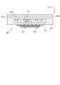
- FIG. 5 is a diagram for explaining the first magnifying optical system 30A and the second magnifying optical system 30B provided in the first light source unit OPU1 and the second light source unit OPU2, respectively.
- the first magnifying optical system 30A is a magnifying optical system for forming a magnified image of the light-emitting portion 231A of each LED chip 23A on a predetermined plane PP.
- the first magnifying optical system 30A has a plurality of lens portions 31A arranged to correspond to the arrangement of the LED chips 23A.
- Each lens portion 31A is a double-telecentric optical system that enlarges and projects the light-emitting portion 231A at a magnification M1 that is equal to or greater than (arrangement pitch P1 of the LED chips 23B)/(length a1 of one side of the light-emitting surface of the light-emitting portion 231A). Note that, for clarity of illustration, FIG. 5 shows only four LED chips 23A (23B) aligned in a row along the Y1 direction.
- the second magnifying optical system 30B is a magnifying optical system for forming a magnified image of the light-emitting portion 231B of each LED chip 23B on a predetermined plane PP.
- the second magnifying optical system 30B has a plurality of lens portions 31B arranged to correspond to the arrangement of the LED chips 23B.
- Each lens portion 31B is a double-telecentric optical system that enlarges and projects the light-emitting portion 231B at a magnification M2 that is equal to or greater than (arrangement pitch P2 of the LED chips 23A)/(length a2 of one side of the light-emitting surface of the light-emitting portion 231B).
- each of the lens units 31A and 31B has four plano-convex lenses, but this is not limited to this, and the lens units 31A and 31B may have, for example, two biconvex lenses or three biconvex lenses. Furthermore, the lens units 31A and 31B may have, for example, a plano-convex lens and a biconvex lens.
- the illumination optical system 80 comprises a first focusing optical system 81A including a first dichroic mirror DM1, a second focusing optical system 81B, a second dichroic mirror DM2, an imaging optical system 83, a fly's eye lens FEL, and a condenser optical system 84.
- the first focusing optical system 81A forms the pupil of the magnified image of the light emitting part 231A formed by the first magnifying optical system 30A. That is, the rear focal position of the first focusing optical system 81A is the position of the pupil.
- the first focusing optical system 81A has a first dichroic mirror DM1 in the middle of the optical path, and reflects at least a part of the light with a peak wavelength of 385 nm. As a result, the light beam is incident on the second dichroic mirror DM2. Note that the first focusing optical system 81A may be configured without the first dichroic mirror DM1.
- the arrangement of the first light source unit OPU1 and the arrangement of each lens of the first focusing optical system 81A may be appropriately adjusted so that the light beam is incident on the second dichroic mirror DM2.
- the first focusing optical system 81A may be configured with one lens, or may be configured with a lens group including multiple lenses.
- the second focusing optical system 81B forms the pupil of the magnified image of the light-emitting section 231B formed by the second magnifying optical system 30B.
- the rear focal position of the second focusing optical system 81B is the pupil position.
- the second focusing optical system 81B may be composed of a single lens, or may be composed of a lens group including multiple lenses.
- the second dichroic mirror DM2 transmits at least a portion of the light with a peak wavelength of 385 nm and reflects at least a portion of the light with a peak wavelength of 365 nm. This forms a composite image by superimposing the pupil image formed by the first focusing optical system 81A and the pupil image formed by the second focusing optical system 81B.
- the second dichroic mirror DM2 forms a composite image by superimposing the pupil image formed by the first focusing optical system 81A and the pupil image formed by the second focusing optical system 81B. That is, the second dichroic mirror DM2 is disposed at a position that is the rear focal position of the first focusing optical system 81A and the rear focal position of the second focusing optical system 81B. As a result, the second dichroic mirror DM2 is Koehler illuminated with the light emitted from the first light source unit OPU1 and the light emitted from the second light source unit OPU2.
- the configuration is not limited to this embodiment, and the first focusing optical system 81A and the second focusing optical system 81B may be configured to perform critical illumination that forms an image of the first light source unit OPU1 and an image of the second light source unit OPU2 on the second dichroic mirror DM2, respectively.
- the illumination unit 90 is provided with a detector DT10 for monitoring light with a peak wavelength of 385 nm, a detector DT20 for monitoring light with a peak wavelength of 365 nm, and a detector DT30 for monitoring light with a peak wavelength of 385 nm and light with a peak wavelength of 365 nm.
- detector DT10 detects the illuminance of light with a peak wavelength of 385 nm reflected by the first dichroic mirror DM1.
- Detector DT20 detects the illuminance of light with a peak wavelength of 365 nm reflected by the second dichroic mirror DM2.
- Detector DT30 detects the illuminance of 385 nm light unintentionally reflected by the second dichroic mirror DM2 and the illuminance of 365 nm light unintentionally transmitted by the second dichroic mirror DM2.
- the detection results of the detectors DT10 to DT30 are output to a control device (not shown), and the control device controls the value of the current supplied to the LED chips 23A and 23B provided in the first light source unit OPU1 and the second light source unit OPU2, respectively, based on the detection results of the detectors DT10 to DT30.
- the imaging optical system 83 is a double-telecentric optical system that projects the composite image created by the second dichroic mirror DM2 at the same magnification onto the incident end of the fly-eye lens FEL. Note that the imaging optical system 83 may also reduce and project the composite image created by the second dichroic mirror DM2 onto the incident end of the fly-eye lens FEL.
- the fly-eye lens FEL is constructed by arranging, for example, a large number of lens elements having positive refractive power densely and vertically so that their optical axes are parallel to the reference optical axis AX.
- Each lens element constituting the fly-eye lens FEL has a rectangular cross section similar to the shape of the illumination field to be formed on the mask MSK (and thus the shape of the exposure area to be formed on the plate P).
- the light beam incident on the fly-eye lens FEL is wavefront split by multiple lens elements, and one light source image is formed on or near the rear focal plane (exit surface) of each lens element.
- a substantial surface light source i.e., a secondary light source, consisting of multiple light source images is formed on or near the rear focal plane (exit surface) of the fly-eye lens FEL.
- the light beam from the secondary light source formed on or near the rear focal plane (exit surface) of the fly-eye lens FEL is incident on an aperture stop 85 arranged nearby.
- the rear focal plane (exit surface) of the fly-eye lens FEL is optically conjugate with the first light source array 20A and the second light source array 20B.
- the aperture stop 85 is positioned at a position that is nearly optically conjugate with the entrance pupil plane of the projection optical system PL, and has a variable opening for defining the range that contributes to the illumination of the secondary light source.
- the aperture stop 85 changes the aperture diameter of the variable opening to set the ⁇ value (the ratio of the aperture diameter of the secondary light source image on the pupil plane of the projection optical system to the aperture diameter of the pupil plane) that determines the illumination conditions to a desired value.
- the light from the secondary light source that passes through the aperture stop 85 is subjected to the focusing action of the condenser optical system 84, and then illuminates the mask MSK, on which a predetermined pattern is formed, in a superimposed manner.
- the wavelengths of the light emitted by the first light source unit OPU1 and the second light source unit OPU2 are not limited to those described above, and the first light source unit OPU1 and the second light source unit OPU2 may be configured by appropriately combining LED chips that emit light having a peak wavelength in the range of 360 to 440 nm.
- the peak wavelength of the light emitted from the light-emitting portion 231A of the LED chip 23A may be in the range of 400 to 410 nm.
- the first light source unit OPU1 may be configured to emit light with a peak wavelength of 405 nm
- the second light source unit OPU2 may be configured to emit light with a peak wavelength of 365 nm.
- the first light source unit OPU1 may be configured to emit light with a peak wavelength of 395 nm
- the second light source unit OPU2 may be configured to emit light with a peak wavelength of 385 nm.
- the combination of the wavelength of the light emitted from the first light source unit OPU1 and the wavelength of the light emitted from the second light source unit OPU2 is not limited to these examples. Note that when the combination of the wavelength of the light emitted from the first light source unit OPU1 and the wavelength of the light emitted from the second light source unit OPU2 is a combination other than that of the first embodiment, it is preferable to change the material of the dichroic mirror appropriately depending on the wavelength to be used.
- the first light source unit OPU1 includes a heat sink 40 and a plurality of LED chips 23A arranged two-dimensionally on the first surface 40a of the heat sink 40.
- the first surface 40a of the heat sink 40 has a plurality of protrusions 401 formed thereon, which protrude from the first surface 40a and overlap at least one of the plurality of LED chips 23A in a plan view.
- This allows the LED chips 23A to be directly mounted on the heat sink 40, so that the LED chips 23A can be cooled more efficiently than when a substrate on which the LED chips 23A are arranged is mounted on a heat sink.
- the size of the first light source unit OPU1 in the Z1 direction can be reduced compared to when a substrate on which the LED chips 23A are arranged is mounted on a heat sink.
- the protrusion 401 extends in the Y1 direction, but the protrusion 401 may extend in the X1 direction.
- the LED chips 23A adjacent to each other in the Y1 direction are connected in series
- the LED chips 23B adjacent to each other in the Y1 direction are connected in series.
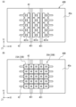
- FIG. 6(A) is a plan view showing a heat sink 40A relating to variant example 1 of the first embodiment
- FIG. 6(B) is a plan view showing the state in which a first light source array 20A and a second light source array 20B are mounted on the heat sink 40A relating to variant example 1.
- the heat sink 40A has a plurality of projections (posts) 401A on the first surface 40a that protrude from the first surface 40a and are spaced apart from one another.
- the plurality of projections 401A each overlap with the LED chip 23A in a plan view.
- the protrusion 401A has a circular planar shape, but the planar shape of the protrusion 401A may be an ellipse or a polygonal shape such as a square or a pentagon.
- the rest of the configuration is the same as in the first embodiment, so a detailed description is omitted.
- the LED chip 23A may be mounted directly to the heat sink 40A using the protrusions 401A spaced apart from each other as in variant example 1. This allows the LED chip 23A to be cooled more efficiently and reduces the size of the first light source unit OPU1 in the Z1 direction compared to mounting a board on which multiple LED chips 23A are arranged to a heat sink.
- Figure 7 (A) is a plan view showing a heat sink 40B relating to variant example 2 of the first embodiment
- Figure 7 (B) is a plan view showing the state in which the first light source array 20A and the second light source array 20B are mounted on the heat sink 40B relating to variant example 2.
- the heat sink 40B has, on the first surface 40a, a number of projections (posts) 401A that protrude from the first surface 40a and are spaced apart from one another, and a number of projections 401 that protrude from the first surface 40a and extend in the Y1 direction.
- the multiple protrusions 401A overlap with the multiple LED chips 23A in a planar view.
- the protrusions 401 overlap with each of the multiple LED chips 23A in a planar view.
- the protrusions 401A and the protrusions 401 are alternately arranged in the X1 direction, but the arrangement of the protrusions 401A and the protrusions 401 is not limited to FIG. 7A.
- the multiple protrusions 401A may be collectively provided on the +X1 side, and the multiple protrusions 401 may be collectively provided on the -X1 side.
- the number of protrusions 401 may be one, or three or more.
- the other configurations are the same as those in the first embodiment, so detailed description will be omitted.
- a protrusion 401A that overlaps each of the multiple LED chips 23A in a planar view may be combined with a protrusion 401 that overlaps each of the multiple LED chips 23A in a planar view.
- the protrusion 401 extends in the Y1 direction, but it may extend in the X1 direction. In this case, the LED chips 23A adjacent in the Y1 direction are connected in series.
- FIG. 8A is a plan view illustrating a heat sink 40C according to the second embodiment
- FIG. 8B is a cross-sectional view taken along line AA of FIG. 8A.
- the heat sink 40C extends in the X1 direction and has a flow path 402A through which a refrigerant flows from a refrigerant inlet 403A provided at one end of the heat sink 40C in the X1 direction to a refrigerant outlet 404A provided at the other end of the heat sink 40C in the X1 direction.
- the heat sink 40C has multiple flow paths 402A corresponding to each row of the LED chips 23A, but one flow path 402A may be provided for each of the multiple rows of the LED chips 23A.
- the heat sink 40C has five protrusions 401 on the first surface 40a, which protrude from the first surface 40a, extend in the Y1 direction, and are spaced apart in the X1 direction.
- the five protrusions 401 are referred to as protrusions 401a, 401b, 401c, 401d, and 401e, in order from the end where the refrigerant inlet 403A is provided. If the widths in the X1 direction of protrusions 401a, 401b, 401c, 401d, and 401e are Wa, Wb, Wc, Wd, and We, respectively, then Wa ⁇ Wb ⁇ Wc ⁇ Wd ⁇ We. That is, in the second embodiment, the closer to the refrigerant inlet 403A, the narrower the width of the protrusions 401 in the X1 direction.
- the refrigerant flows in the flow path 402A in the -X1 direction, so the cooling effect of the refrigerant on the LED chip 23A is higher the closer it is to the refrigerant inlet 403A.
- the protrusion 401 which has a narrow width in the X1 direction and a low cooling effect, near the refrigerant inlet 403A, where the cooling effect of the refrigerant on the LED chip 23A is high, and arranging the protrusion 401, which has a wide width in the X1 direction and a high cooling effect, near the refrigerant outlet 404A, where the cooling effect of the refrigerant on the LED chip 23A is low, it is possible to reduce uneven cooling of the LED chip 23A and to cool the LED chip 23A approximately uniformly.
- FIG. 9A is a plan view illustrating a heat sink 40D according to a first modified example of the second embodiment
- FIG. 9B is a cross-sectional view taken along line AA of FIG. 9A.
- a protrusion 401A is provided on the first surface 40a of the heat sink 40D, protruding from the first surface 40a and overlapping with the LED chip 23A in a plan view.
- the planar shape of the protrusion 401A is a square.
- the protrusions 401A that are closest to the refrigerant inlet 403A are designated as protrusions 401Aa, and the protrusions 401A are designated as protrusions 401Ab, 401Ac, 401Ad, and 401Ae in the -X direction. If the lengths of one side of the protrusions 401Aa, 401Ab, 401Ac, 401Ad, and 401Ae are La, Lb, Lc, Ld, and Le, respectively, La ⁇ Lb ⁇ Lc ⁇ Ld ⁇ Le.
- the area of the upper surface of the protrusions 401A becomes smaller the closer to the end where the refrigerant inlet 403A is provided.
- the other configurations are the same as those in the second embodiment, and detailed explanations are omitted.
- the refrigerant flows in the flow path 402A in the -X1 direction, so the cooling effect of the refrigerant on the LED chip 23A is higher at a position closer to the refrigerant inlet 403A.
- the closer the protrusion 401A is to the refrigerant inlet 403A the smaller the area of the upper surface, so the cooling effect of the protrusion 401A on the LED chip 23A is lower at the protrusion 401A closer to the refrigerant inlet 403A.
- the protrusion 401A with a small upper surface area and low cooling effect near the refrigerant inlet 403A, where the cooling effect of the refrigerant on the LED chip 23A is high, and arranging the protrusion 401A with a large upper surface area and high cooling effect near the refrigerant outlet 404A, where the cooling effect of the refrigerant on the LED chip 23A is low, the cooling unevenness of the LED chip 23A can be reduced and the LED chip 23A can be cooled approximately uniformly.
- the planar shape of the protrusion 401A may be other shapes, such as a circular shape.
- FIG. 10A is a plan view illustrating a heat sink 40E according to a second modification of the second embodiment
- FIG. 10B is a cross-sectional view taken along line AA of FIG. 10A.
- the heat sink 40E has, on the first surface 40a, protrusions (posts) 401A that overlap with each of the multiple LED chips 23A in a planar view, and protrusions 401 that extend in the Y1 direction and overlap with each of the multiple LED chips 23A in a planar view.
- the protrusion 401A has a square planar shape with a side length of L.
- the width of the protrusion 401 in the X1 direction is W.
- the length L of one side of the protrusion 401A is equal to the width W of the protrusion 401 in the X1 direction. Therefore, the area of the upper surface of the protrusion 401A is smaller than the area of the upper surface of the protrusion 401.
- the protrusion 401A and the protrusion 401 are provided in this order from one end where the refrigerant inlet 403A is provided to the other end where the refrigerant outlet 404A is provided.
- the rest of the configuration is the same as in the second embodiment, so detailed description will be omitted.
- the protrusion 401A which has a small upper surface area and a low cooling effect, near the refrigerant inlet 403A, where the refrigerant has a high cooling effect on the LED chip 23A
- the protrusion 401 which has a large upper surface area and a high cooling effect, near the refrigerant outlet 404A, where the refrigerant has a low cooling effect on the LED chip 23A
- uneven cooling of the LED chip 23A can be reduced and the LED chip 23A can be cooled approximately uniformly.
- the planar shape of the protrusion 401A may be other shapes, such as a circular shape.
- FIG. 11 is a cross-sectional view illustrating a heat sink 40F according to the third embodiment.
- the heat sink 40F has an internal space 410 and a working fluid 411 held in the internal space 410.
- the internal space 410 is disposed between the first surface 40a and the flow path 402A. That is, in the heat sink 40E, a vapor chamber is formed between the first surface 40a and the flow path 402A.
- the working fluid 411 held in the internal space 410 evaporates due to the heat from the LED chip 23A.
- the evaporated working fluid 411 moves within the internal space 410 as shown by arrow AR3, diffusing the heat.
- the diffused working fluid 411 is cooled and liquefied by the refrigerant flowing through the flow path 402A. In this way, the working fluid 411 repeatedly evaporates and liquefies, thereby cooling the heat source (LED chips 23A and 23B).
- the vapor chamber has high thermal conductivity and is flat, allowing heat to be diffused instantly over a wide area. Therefore, the heat sink 40F can cool the LED chip 23A more efficiently than a heat sink that does not have a vapor chamber.
- heat sink 40C The rest of the configuration is the same as the heat sink 40C according to the second embodiment, so a detailed description will be omitted.
- the heat sinks 40, 40A to 40E according to the first and second embodiments and their modified examples may have a vapor chamber.
- FIG. 12 is a diagram showing a preferred configuration of a lighting unit 90A when using a heat sink 40F according to the third embodiment.
- the light emitting surface of the light emitting portion 231A of the LED chip 23A and the light emitting surface of the light emitting portion 231B of the LED chip 23B face the direction of gravity, as shown in FIG. 12, so that the liquefied working fluid 411 moves by gravity toward the LED chips 23A and 23B.
- the illumination optical system 80A of the illumination unit 90A includes a third focusing optical system 81C, a fourth focusing optical system 81D including a third dichroic mirror DM3, a second dichroic mirror DM2, an imaging optical system 83, a fly's eye lens FEL, and a condenser optical system 84.
- the third focusing optical system 81C forms the pupil of the enlarged image of the light-emitting section 231A formed by the first magnifying optical system 30A.
- the rear focal position of the third focusing optical system 81C is the pupil position.
- the arrangement of the first light source unit OPU1 and the arrangement of each lens of the third focusing optical system 81C are adjusted so that the light beam is incident on the second dichroic mirror DM2.
- the fourth focusing optical system 81D forms the pupil of the magnified image of the light-emitting section 231B formed by the second magnifying optical system 30B.
- the rear focal position of the fourth focusing optical system 81D is the pupil position.
- the fourth focusing optical system 81D has a third dichroic mirror DM3 in the middle of the optical path, which reflects at least a portion of the light with a peak wavelength of 365 nm. This causes the light beam to be incident on the second dichroic mirror DM2.
- the configurations and functions of the second dichroic mirror DM2, the imaging optical system 83, the fly-eye lens FEL, and the condenser optical system 84 are the same as those in FIG. 2, so detailed explanations are omitted.
- the first light source array 20A and the second light source array 20B are respectively mounted on the heat sinks 40, 40A to 40E having the same configuration, but this is not limited to the above.
- the configuration of the heat sink on which the first light source array 20A is mounted may be different from the configuration of the heat sink on which the second light source array 20B is mounted.
- the first light source array 20A may be mounted on the heat sink 40 according to the first embodiment
- the second light source array 20B may be mounted on the heat sink 40C according to the second embodiment.
- the heat sink has flow paths 402, 402A through which the refrigerant flows, but this is not limited to this.
- the heat sink may be, for example, a fin-type heat sink.
- the heat sink does not have to be a microchannel heat sink.
- the refrigerant inlets 403, 403A and the refrigerant outlets 404, 404A are provided on the side of the heat sink, but they may be provided on the first surface 40a or the second surface 40b of the heat sink, respectively.
- the thickness of the heat sink is 7 mm or less.
- the thickness of the heat sink refers to the length from the upper surface of the protrusion 401 and/or the protrusion 401A formed on the first surface 40a of the heat sink to the second surface 40b.
- the length from the upper surface of the protrusion 401 and/or the protrusion 401A to the first surface 40a is preferably 500 ⁇ m or less, and more preferably 150 to 200 ⁇ m.
- the upper limit of the thickness of the substrate that can be carried in may be limited to about 7 mm, and a wiring layer may not be formed on a thick substrate.
- the thickness of the heat sink may be 7 mm or more.
- the protrusions 401, 401A are described as being part of the heat sink, but this is not limiting.
- the protrusions 401, 401A may be a member different from the heat sink (a member separate from the heat sink) that comes into contact with the first surface 40a of the heat sink.
- the protrusions 401, 401A may be formed by fixing (soldering, bonding) a member different from the heat sink to the first surface 40a.
- the protrusions 401, 401A may be formed from the same material as the heat sink, or from a different material.
- the protrusions 401, 401A are formed from a material different from the heat sink, it is preferable that the protrusions 401, 401A are made of a metal with high thermal conductivity.
- the illumination unit 90, 90A includes the first light source unit OPU1, the second light source unit OPU2, and the illumination optical system 80, 80A including the second dichroic mirror DM2, but this is not limited to the above.
- the illumination unit 90, 90A may include only one of the first light source unit OPU1 and the second light source unit OPU2.
- the illumination optical system 80, 80A may have any configuration as long as it can guide the light emitted from the first light source unit OPU1 or the second light source unit OPU2 to the mask MSK.
- the flow path 402 has a serpentine shape, but the flow path 402A in the second embodiment may be applied to the first embodiment and its modified example.
- Exposure apparatus 20A First light source array 20B Second light source array 40a First surface 40b Second surface 23A, 23B LED chip 40, 40A, 40B, 40C, 40D, 40E, 40F Heat sink 80, 80A Illumination optical system 90, 90A Illumination unit 100 Projection optical unit 231A, 231B Light emitting portion 401, 401A Protrusion 402, 402A Flow path 403, 403A Coolant inlet 404, 404A Coolant outlet DM2 Second dichroic mirror MSK Mask OPU1 First light source unit OPU2 Second light source unit PL Projection optical system P Glass substrate
Landscapes
- Physics & Mathematics (AREA)
- General Physics & Mathematics (AREA)
- Health & Medical Sciences (AREA)
- Engineering & Computer Science (AREA)
- Atmospheric Sciences (AREA)
- Toxicology (AREA)
- Life Sciences & Earth Sciences (AREA)
- Environmental & Geological Engineering (AREA)
- Epidemiology (AREA)
- Public Health (AREA)
- Exposure And Positioning Against Photoresist Photosensitive Materials (AREA)
- Cooling Or The Like Of Semiconductors Or Solid State Devices (AREA)
- Arrangement Of Elements, Cooling, Sealing, Or The Like Of Lighting Devices (AREA)
Priority Applications (6)
| Application Number | Priority Date | Filing Date | Title |
|---|---|---|---|
| PCT/JP2023/014075 WO2024209586A1 (ja) | 2023-04-05 | 2023-04-05 | 光源ユニット、照明ユニット、露光装置、及び露光方法 |
| JP2025512473A JPWO2024209913A1 (https=) | 2023-04-05 | 2024-03-18 | |
| KR1020257032366A KR20250160467A (ko) | 2023-04-05 | 2024-03-18 | 광원 유닛, 조명 유닛, 노광 장치, 및 노광 방법 |
| CN202480023500.9A CN120958387A (zh) | 2023-04-05 | 2024-03-18 | 光源单元、照明单元、曝光装置、以及曝光方法 |
| PCT/JP2024/010439 WO2024209913A1 (ja) | 2023-04-05 | 2024-03-18 | 光源ユニット、照明ユニット、露光装置、及び露光方法 |
| TW113110265A TWI915769B (zh) | 2023-04-05 | 2024-03-20 | 光源單元、照明單元、曝光裝置、以及曝光方法 |
Applications Claiming Priority (1)
| Application Number | Priority Date | Filing Date | Title |
|---|---|---|---|
| PCT/JP2023/014075 WO2024209586A1 (ja) | 2023-04-05 | 2023-04-05 | 光源ユニット、照明ユニット、露光装置、及び露光方法 |
Publications (1)
| Publication Number | Publication Date |
|---|---|
| WO2024209586A1 true WO2024209586A1 (ja) | 2024-10-10 |
Family
ID=92971823
Family Applications (2)
| Application Number | Title | Priority Date | Filing Date |
|---|---|---|---|
| PCT/JP2023/014075 Ceased WO2024209586A1 (ja) | 2023-04-05 | 2023-04-05 | 光源ユニット、照明ユニット、露光装置、及び露光方法 |
| PCT/JP2024/010439 Ceased WO2024209913A1 (ja) | 2023-04-05 | 2024-03-18 | 光源ユニット、照明ユニット、露光装置、及び露光方法 |
Family Applications After (1)
| Application Number | Title | Priority Date | Filing Date |
|---|---|---|---|
| PCT/JP2024/010439 Ceased WO2024209913A1 (ja) | 2023-04-05 | 2024-03-18 | 光源ユニット、照明ユニット、露光装置、及び露光方法 |
Country Status (4)
| Country | Link |
|---|---|
| JP (1) | JPWO2024209913A1 (https=) |
| KR (1) | KR20250160467A (https=) |
| CN (1) | CN120958387A (https=) |
| WO (2) | WO2024209586A1 (https=) |
Citations (5)
| Publication number | Priority date | Publication date | Assignee | Title |
|---|---|---|---|---|
| JP2006332077A (ja) * | 2005-05-23 | 2006-12-07 | Nikon Corp | 光源ユニット、照明光学装置、露光装置、および露光方法 |
| JP2012134564A (ja) * | 2004-09-10 | 2012-07-12 | Seoul Semiconductor Co Ltd | 発光素子及びその製造方法 |
| JP2015529396A (ja) * | 2012-08-22 | 2015-10-05 | フレックス‐エヌ‐ゲート アドバンスト プロダクト ディベロップメント エルエルシー | Ledヘッドランプ用マイクロチャネルヒートシンク |
| JP2017187545A (ja) * | 2016-04-01 | 2017-10-12 | シーシーエス株式会社 | 光照射装置 |
| WO2021251090A1 (ja) * | 2020-06-08 | 2021-12-16 | 株式会社ブイ・テクノロジー | 露光用の光源装置、照明装置、露光装置、及び露光方法 |
Family Cites Families (3)
| Publication number | Priority date | Publication date | Assignee | Title |
|---|---|---|---|---|
| JP4587170B2 (ja) | 2005-01-20 | 2010-11-24 | キヤノン株式会社 | 露光装置及びデバイスの製造方法 |
| JP2010274256A (ja) * | 2009-01-29 | 2010-12-09 | Kyocera Corp | 光照射ヘッド、露光デバイス、画像形成装置、液滴硬化装置、および液滴硬化方法 |
| JP4914998B1 (ja) * | 2010-11-17 | 2012-04-11 | 国立大学法人九州工業大学 | Ledモジュール装置及びその製造方法 |
-
2023
- 2023-04-05 WO PCT/JP2023/014075 patent/WO2024209586A1/ja not_active Ceased
-
2024
- 2024-03-18 KR KR1020257032366A patent/KR20250160467A/ko active Pending
- 2024-03-18 WO PCT/JP2024/010439 patent/WO2024209913A1/ja not_active Ceased
- 2024-03-18 JP JP2025512473A patent/JPWO2024209913A1/ja active Pending
- 2024-03-18 CN CN202480023500.9A patent/CN120958387A/zh active Pending
Patent Citations (5)
| Publication number | Priority date | Publication date | Assignee | Title |
|---|---|---|---|---|
| JP2012134564A (ja) * | 2004-09-10 | 2012-07-12 | Seoul Semiconductor Co Ltd | 発光素子及びその製造方法 |
| JP2006332077A (ja) * | 2005-05-23 | 2006-12-07 | Nikon Corp | 光源ユニット、照明光学装置、露光装置、および露光方法 |
| JP2015529396A (ja) * | 2012-08-22 | 2015-10-05 | フレックス‐エヌ‐ゲート アドバンスト プロダクト ディベロップメント エルエルシー | Ledヘッドランプ用マイクロチャネルヒートシンク |
| JP2017187545A (ja) * | 2016-04-01 | 2017-10-12 | シーシーエス株式会社 | 光照射装置 |
| WO2021251090A1 (ja) * | 2020-06-08 | 2021-12-16 | 株式会社ブイ・テクノロジー | 露光用の光源装置、照明装置、露光装置、及び露光方法 |
Also Published As
| Publication number | Publication date |
|---|---|
| JPWO2024209913A1 (https=) | 2024-10-10 |
| WO2024209913A1 (ja) | 2024-10-10 |
| KR20250160467A (ko) | 2025-11-13 |
| CN120958387A (zh) | 2025-11-14 |
| TW202505310A (zh) | 2025-02-01 |
Similar Documents
| Publication | Publication Date | Title |
|---|---|---|
| JP4678493B2 (ja) | 光源ユニット、照明光学装置、露光装置、および露光方法 | |
| KR20170091905A (ko) | 노광용 광원모듈 유닛 및 그 광원모듈 유닛이 구비된 노광장치 | |
| WO2024209586A1 (ja) | 光源ユニット、照明ユニット、露光装置、及び露光方法 | |
| TWI915769B (zh) | 光源單元、照明單元、曝光裝置、以及曝光方法 | |
| JP7806909B2 (ja) | 照明ユニット、露光装置、及び露光方法 | |
| TWI855790B (zh) | 光源單元、照明單元、曝光裝置、及曝光方法 | |
| TWI876438B (zh) | 光源單元、照明單元、曝光裝置、及曝光方法 | |
| TWI915658B (zh) | 光源單元、照明單元、曝光裝置、及曝光方法 | |
| WO2024038538A1 (ja) | 光源ユニット、照明ユニット、露光装置、及び露光方法 | |
| KR20250160466A (ko) | 구동 방법, 광원 유닛, 조명 유닛, 노광 장치, 및 노광 방법 | |
| KR20210122109A (ko) | 광원 장치, 조명 장치 및 노광 장치 | |
| TWI920814B (zh) | 曝光裝置 | |
| WO2025079172A1 (ja) | 光源ユニット、照明ユニット、露光装置、及び露光方法 | |
| JP2006253486A (ja) | 照明装置、投影露光方法、投影露光装置、及びマイクロデバイスの製造方法 | |
| KR20250060918A (ko) | 합성 광학 소자, 조명 유닛, 노광 장치, 및 노광 방법 | |
| WO2025094252A1 (ja) | 露光装置 | |
| WO2025013286A1 (ja) | 照明ユニット、露光装置、及び露光方法 | |
| KR20260060422A (ko) | 광원 유닛, 조명 유닛, 노광 장치, 및 노광 방법 | |
| JP2026056837A (ja) | 光源装置、露光装置、及び物品の製造方法 |
Legal Events
| Date | Code | Title | Description |
|---|---|---|---|
| 121 | Ep: the epo has been informed by wipo that ep was designated in this application |
Ref document number: 23931998 Country of ref document: EP Kind code of ref document: A1 |
|
| NENP | Non-entry into the national phase |
Ref country code: DE |
|
| 122 | Ep: pct application non-entry in european phase |
Ref document number: 23931998 Country of ref document: EP Kind code of ref document: A1 |