WO2024209562A1 - 電子部品、電気機器、バスバー、電子部品の製造方法および電気機器の製造方法 - Google Patents
電子部品、電気機器、バスバー、電子部品の製造方法および電気機器の製造方法 Download PDFInfo
- Publication number
- WO2024209562A1 WO2024209562A1 PCT/JP2023/013995 JP2023013995W WO2024209562A1 WO 2024209562 A1 WO2024209562 A1 WO 2024209562A1 JP 2023013995 W JP2023013995 W JP 2023013995W WO 2024209562 A1 WO2024209562 A1 WO 2024209562A1
- Authority
- WO
- WIPO (PCT)
- Prior art keywords
- bus bar
- hole
- busbar
- contact
- region
- Prior art date
- Legal status (The legal status is an assumption and is not a legal conclusion. Google has not performed a legal analysis and makes no representation as to the accuracy of the status listed.)
- Ceased
Links
Images



Classifications
-
- H—ELECTRICITY
- H01—ELECTRIC ELEMENTS
- H01F—MAGNETS; INDUCTANCES; TRANSFORMERS; SELECTION OF MATERIALS FOR THEIR MAGNETIC PROPERTIES
- H01F27/00—Details of transformers or inductances, in general
- H01F27/28—Coils; Windings; Conductive connections
- H01F27/29—Terminals; Tapping arrangements for signal inductances
-
- H—ELECTRICITY
- H01—ELECTRIC ELEMENTS
- H01R—ELECTRICALLY-CONDUCTIVE CONNECTIONS; STRUCTURAL ASSOCIATIONS OF A PLURALITY OF MUTUALLY-INSULATED ELECTRICAL CONNECTING ELEMENTS; COUPLING DEVICES; CURRENT COLLECTORS
- H01R4/00—Electrically-conductive connections between two or more conductive members in direct contact, i.e. touching one another; Means for effecting or maintaining such contact; Electrically-conductive connections having two or more spaced connecting locations for conductors and using contact members penetrating insulation
- H01R4/28—Clamped connections, spring connections
- H01R4/30—Clamped connections, spring connections utilising a screw or nut clamping member
- H01R4/34—Conductive members located under head of screw
-
- H—ELECTRICITY
- H01—ELECTRIC ELEMENTS
- H01R—ELECTRICALLY-CONDUCTIVE CONNECTIONS; STRUCTURAL ASSOCIATIONS OF A PLURALITY OF MUTUALLY-INSULATED ELECTRICAL CONNECTING ELEMENTS; COUPLING DEVICES; CURRENT COLLECTORS
- H01R4/00—Electrically-conductive connections between two or more conductive members in direct contact, i.e. touching one another; Means for effecting or maintaining such contact; Electrically-conductive connections having two or more spaced connecting locations for conductors and using contact members penetrating insulation
- H01R4/58—Electrically-conductive connections between two or more conductive members in direct contact, i.e. touching one another; Means for effecting or maintaining such contact; Electrically-conductive connections having two or more spaced connecting locations for conductors and using contact members penetrating insulation characterised by the form or material of the contacting members
Definitions
- the present invention relates to electronic components, electrical equipment, bus bars, methods for manufacturing electronic components, and methods for manufacturing electrical equipment.
- the electronic component and the contact member are in contact with each other to establish electrical continuity. If the contact resistance at the contact surface is large, at least one of the following problems will occur: the current passing between the electronic component and the contact member will decrease, or the material around the contact surface will deform due to heat generation.
- the present invention has been made in consideration of the above-mentioned problems, and provides an electronic component, an electronic device, a bus bar, a method for manufacturing an electronic component, and a method for manufacturing an electronic device that reduce current loss.
- the electronic device of the present invention is an electrical device having an electronic component including a main body including an electronic element and a bus bar electrically connected to the electronic element, and a second bus bar in contact with the bus bar, the bus bar having a hole, an uneven area having an uneven structure around the hole on the contact surface where the hole opens, the second bus bar in contact with the contact surface on the opposing surface opposite the contact surface, and a top portion which is a protruding tip portion of the uneven structure is fitted into the second bus bar.
- the busbar of the present invention is a conductor having a hole, and is characterized in that an uneven area having an uneven structure is formed around the hole on the contact surface where the hole opens.
- the method for manufacturing an electronic component of the present invention is a method for manufacturing an electronic component that includes a main body including an electronic element and a bus bar electrically connected to the electronic element, and includes a forming step in which a hole is formed in a region where a hole is to be formed, and an imprinting step in which a pressing member is pressed against the hole or the periphery of the region where a hole is to be formed to form a concave-convex structure around the hole or the region where a hole is to be formed, and is characterized in that the forming step and the imprinting step are performed simultaneously or sequentially.
- the method for manufacturing an electronic device of the present invention is a method for manufacturing an electric device having an electronic component including a main body including an electronic element and a bus bar electrically connecting to the electronic element, and a second bus bar in contact with the bus bar, the bus bar having a hole, an uneven area having an uneven structure around the hole on a contact surface where the hole opens, the bus bar and the second bus bar are arranged so that the contact surface faces an opposing surface of the second bus bar, and the contact surface and the opposing surface are pressed against each other so that a part of the uneven structure fits into the second bus bar.
- the busbar has an uneven structure, which allows the uneven structure to bite into the contact member that comes into contact with the busbar, thereby making contact with the busbar. This allows the contact area between the busbar and the contact member to be increased, or allows the busbar to bite into the contact member and press against it, reducing contact resistance and suppressing current loss.
- Fig. 1A is a perspective view showing an example of an electronic component according to a first embodiment of the present invention
- Fig. 1B is a front view of a first bus bar
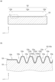
- Fig. 2(a) is a cross-sectional view taken along the dashed line in Fig. 1(b) of the electronic component according to the first embodiment, as viewed in the direction of the arrows II-II.
- Fig. 2(b) is an enlarged view of a region X in Fig. 2(a).
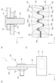
- Fig. 3(a) is a schematic diagram of an electronic device according to a first embodiment
- Fig. 3(b) is a schematic diagram of a joint portion between a first bus bar and a second bus bar
- FIG. 3(c) is a schematic enlarged cross-sectional view illustrating a joint mode between a peripheral portion of the first bus bar and the second bus bar.
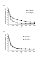
- 4(a) is a graph showing an example of the contact resistance value of a first busbar having a concave-convex structure and a busbar not having a concave-convex structure
- FIG 4(b) is a graph showing an example of the contact resistance value of a first busbar having an oxide film and a first busbar not having an oxide film.
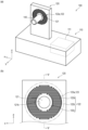
- Fig. 5(a) is a perspective view showing an example of an electronic component according to a second embodiment of the present invention
- Fig. 5(b) is a front view of a first bus bar.
- FIG. 6(a) is a cross-sectional view of the electronic component according to the second embodiment taken along the dashed line in Fig. 5(b) as viewed in the direction of the arrow V-V.
- Fig. 6(b) is an enlarged view of region Z in Fig. 6(a).
- Fig. 6(c) is an enlarged view of region Y in Fig. 6(a).
- 7A and 7B are schematic enlarged cross-sectional views illustrating a joining manner between an outer peripheral portion of a first bus bar and a second bus bar in an electronic component according to a second embodiment, respectively.
- the various components of the electronic components, electrical devices, and bus bars of the present invention do not need to be independent entities, and it is permitted that multiple components are formed as a single member, that one component is formed from multiple members, that one component is part of another component, that part of one component overlaps with part of another component, etc.
- the manufacturing method of the electronic component or electronic device of the present invention may be described using a number of steps described in order, but the order of the steps does not limit the order or timing of performing the number of steps. Therefore, when implementing the manufacturing method of the electronic component or electronic device of the present invention, the order of the number of steps may be changed to the extent that does not interfere with the content, and some or all of the timing of performing the number of steps may overlap with each other.
- FIG. 1A is a perspective view showing an example of an electronic component 100 according to a first embodiment of the present invention.
- the electronic component 100 includes a main body 110 and a bus bar (first bus bar 120).
- the main body 110 includes an electronic element 111.
- the first bus bar 120 is electrically connected to the electronic element 111.
- the first bus bar 120 has a hole 121.
- an uneven region 122a having an uneven structure 123 (see FIG. 1( b )) is formed around the hole 121.
- First busbar 120 has uneven structure 123 (see FIG. 1( b )), which allows uneven structure 123 to bite into a contact member (second busbar 200 (see FIG.
- first busbar 120 bites into the contact member, causing first busbar 120 to be pressed against the contact member, and this pressure may bond the surfaces of first busbar 120 and the contact member together. This reduces contact resistance and suppresses current loss.
- the electronic component 100 refers to a part including an electronic element 111 that constitutes an electronic circuit.
- a component that can be connected to or removed from a contact member is called the electronic component 100.
- the electronic element 111 is a component included in the electronic component 100, and is a part that constitutes an electronic circuit including a core or a coil.
- the main function of the electronic component 100 is realized by the electronic element 111.
- the electronic element 111 may include a core or a coil, and the electronic component 100 as a whole may be a coil component such as an inverter, an inductor, a transformer, or an antenna.
- the electronic component 100 in this embodiment is an in-vehicle electronic component that constitutes an electric device mounted on a vehicle body such as an automobile. More specifically, battery devices such as lithium ion batteries and all-solid-state batteries mounted on electric vehicles are examples of electric devices. Examples of the electronic component 100 include various reactors that are connected to an electric device that is an in-vehicle battery device and to which a current is applied during charging or discharging.
- the main body 110 is a part of the electronic component 100 and includes the electronic element 111. It is preferable that the main body 110 has the electronic element 111 therein.
- the entire main body 110 may be covered with a molded resin or the like.
- the main body 110 is a member whose longitudinal direction is the x-axis direction, but the main body 110 may have any shape.
- the busbar is made of a material having electrical conductivity, such as a metal containing copper.
- the busbar has a cross section (a cross section cut horizontally with respect to a contact surface 122 described later) that is larger than that of a wire and has an overall shape that is approximately rod-like or plate-like.
- the electronic component 100 or an electric device 1 described later has a first busbar 120 or a second busbar 200 as a busbar.
- the direction in which the busbar has the largest dimension among the height direction, width direction, and thickness direction of the busbar may be referred to as the longitudinal direction of the busbar.
- the longitudinal direction of the first busbar 120 and the second busbar 200 (see FIG. 3A) is the z-axis direction.
- the cross section of the first busbar 120 is a cross section cut horizontally with respect to the contact surface 122, in other words, a cross section of the first busbar 120 cut perpendicularly to the plate thickness direction (y direction).
- the cross section of the busbar may be a polygon such as a rectangle, or may be a circle or an ellipse.
- the first bus bar 120 is a member for electrically connecting a contact member connected to the electronic component 100 and the electronic element 111.
- a part of the base end side (-z direction) of the first bus bar 120 is embedded inside the main body 110, and another part of the tip side (z direction) protrudes outward from the main body 110.
- the outer edge of the tip of the first bus bar 120 is semicircular in shape along a peripheral wall surface 121b that defines a hole 121 described later.
- the first bus bar 120 is electrically connected to the electronic element 111 inside the main body 110.
- the electronic component 100 has one first bus bar 120 , but the electronic component 100 may have a plurality of first bus bars 120 .
- the hole 121 of the first busbar 120 is a hole into which the shaft member 140 (see FIG. 3A), which will be described later, is inserted.
- the hole 121 may be a through hole as in the present embodiment, or may be a concave portion with a bottom.
- the hole 121 is defined by a peripheral wall surface 121b, which is also a part of the outer surface of the first busbar 120. It is preferable that the penetration direction or depth direction of the hole 121 (hereinafter collectively referred to as the penetration direction; y-axis direction) is a direction perpendicular to the longitudinal direction (z-axis direction) of the first busbar 120. Specifically, as shown in FIG.
- the penetration direction of the hole 121 is the same direction as the direction (y-axis direction) in which the first busbar 120 and the contact member (such as the second busbar 200 (see FIG. 3A)) that contacts the first busbar 120 are arranged.
- the shape of the hole 121 as viewed from the penetration direction of the hole 121 is circular, but is not limited thereto.
- the shape may be a polygon such as a rectangle, or may be an ellipse in addition to a circle.
- the shape and dimensions of the hole 121 in the penetration direction of the hole 121 are preferably sufficient to allow the shaft member 140 (see FIG. 3A) to be inserted therethrough. That is, as shown in FIG.
- the shaft member 140 when the shaft member 140 is inserted into the hole 121, it is preferable that a gap is generated between the peripheral wall surface 121b of the hole 121 and the peripheral surface of the shaft member 140.
- the radius of the hole 121 is larger than the radius of the cross section of the shaft member 140 (particularly the shaft portion 142). 1B, the hole 121 is open at least in the contact surface 122.
- the hole 121 is open in the contact surface 122 and in a back surface (a surface of the first bus bar 120 facing in the -y direction) that is disposed on the opposite side of the contact surface 122.
- the contact surface 122 is a partial surface area of the outer surface of the first bus bar 120.
- the contact surface 122 is a partial surface area that is in contact with a contact destination member (such as the second bus bar 200) or is to be in contact with the contact destination member.
- the contact surface 122 may be composed only of a surface area that is in contact with or is to be in contact with the contact destination member, or may include a surface area around the surface area that is not in contact with the contact destination member or is not to be in contact with the contact destination member.
- the uneven region 122a is a partial region of the contact surface 122, and refers to a surface region in which the uneven structure 123 is formed.
- the uneven region 122a is a region that is larger in unevenness than other regions (e.g., the outer peripheral portion 122b) adjacent to the outside of the uneven region 122a.
- the uneven region 122a is a flat region that extends in the approximate extension direction of the contact surface 122.
- the uneven region 122a formed around the hole 121 means that the uneven region 122a is formed on a part of the contact surface 122 close to the hole 121.
- the shortest distance along the contact surface 122 between the hole 121 and the uneven region 122a is preferably smaller than the protruding dimension of the shaft head 141 described later.
- the protruding dimension of the shaft head 141 is the height of the outer peripheral edge of the shaft head 141 based on the peripheral surface of the shaft 142.
- it is preferable that the distance is smaller than the radius of the hole 121. More preferably, the distance is zero.
- the shaft member 140 By arranging the uneven region 122a around the hole portion 121 in this manner, the shaft member 140 (particularly the shaft head portion 141) can sufficiently apply stress for the uneven structure 123 described later to fit into the contacting member (the second bus bar 200, etc.).
- the uneven region 122a is formed so as to surround the periphery of the hole 121.
- the uneven region 122a is formed outward in all directions in the radial direction of the hole 121.
- the radial direction of the hole 121 refers to a direction extending in the penetrating direction of the hole 121 and passing through the center of the hole 121 toward the peripheral wall surface 121b that defines the hole 121.
- the uneven region 122a may be formed outward in a part of the radial direction of the hole 121.
- the uneven region 122a is a partial surface region of one face (face facing the y direction) having the contact surface 122 on the outer surface of the first bus bar 120.
- a part or all of the outer periphery of the uneven region 122a is preferably located more inward than the outer periphery of the first bus bar 120.
- uneven region 122a may be formed in a part (hereinafter also referred to as overlapping part) of the surface facing the y direction that overlaps with second bus bar 200 as seen in the penetration direction of hole 121.
- the outer periphery of uneven region 122a may be located outside or inside the overlapping part as seen in the penetration direction of hole 121.
- the uneven structure 123 is a structure having a plurality of recesses or protrusions.
- the uneven region 122a as a whole has the uneven structure 123, and thus has a rough surface having a larger surface roughness than the surrounding region of the uneven region 122a (such as the outer periphery 122b described later).
- the recesses in uneven structure 123 are parts in the uneven region that are arranged on the protruding inner side of first busbar 120
- the protrusions in uneven structure 123 are parts in uneven region 122a that are arranged on the protruding outer side of first busbar 120.
- the uneven structure 123 in this embodiment is formed by two or more bottomed grooves 123a aligned with each other.
- the grooves 123a are defined by a bottom (groove bottom 123a1 (see FIG. 2B)) and a pair of walls (groove wall 123a2 (see FIG. 2B)) sandwiching the groove bottom 123a1.
- the grooves 123a aligned with each other means that the extension directions of the respective grooves 123a have the same directional components, and preferably the grooves 123a are approximately parallel to each other.
- the extension direction of the grooves 123a may be linear as in this embodiment, or may be wavy.
- the shape of the multiple grooves 123a may be concentric circles with different radii. That is, the extension direction of the grooves 123a may be circular. Even when the grooves 123a are wavy or circular, it is preferable that adjacent grooves 123a are aligned with each other.
- the plurality of substantially linear grooves 123a extend in the longitudinal direction (z-axis direction) of the first bus bar 120.
- the plurality of grooves 123a are continuously arranged in a direction perpendicular to the longitudinal direction (x-axis direction). As shown in FIG. 3A, in this embodiment, the first bus bar 120 and the second bus bar 200 are arranged in the longitudinal direction (z-axis direction) of the first bus bar 120 while being in contact with each other with parts of each of them overlapping in the y-axis direction.
- the grooves 123a By arranging the grooves 123a extending in the longitudinal direction of the first bus bar 120 in a direction perpendicular to the longitudinal direction, the contact surface between the first bus bar 120 and the second bus bar 200 is unlikely to shift laterally in a direction intersecting the longitudinal direction.
- the grooves 123a may extend in a direction perpendicular to the longitudinal direction of the first bus bar 120, and the plurality of grooves 123a may be arranged in the longitudinal direction.
- the widths of the groove bottom 123a1 and top 123b, as well as the inclination angle of the groove wall 123a2 are changed in Figures 1(a), 1(b) and 2(a) compared to those of the groove 123a in Figures 2(b) and 3(c).
- the uneven structure 123 is composed of a plurality of grooves 123a, but instead of this embodiment, the uneven structure 123 may be composed of a plurality of scattered protrusions (e.g., protrusions having a cone or pyramid shape).
- the uneven structure 123 in this embodiment can be said to have a plurality of protruding portions 123e.
- the protruding portion 123e is a portion protruding from the protruding inner side of the first bus bar 120 toward the protruding outer side, and is a part of the first bus bar 120.
- the protruding portion 123e in this embodiment is a part of the first bus bar 120 sandwiched between one groove 123a and another groove 123a adjacent to the one groove 123a. More specifically, the protruding portion 123e is a part of the first bus bar 120 defined by the groove wall portion 123a2 and the top portion 123b that define the groove 123a.
- the protruding portion 123e in this embodiment extends in a substantially linear extension direction along the groove 123a.
- the width of the protruding portion 123e is preferably smaller toward the protruding direction of the uneven structure 123.
- the protruding dimension of the protruding portion 123e is preferably larger than the width dimension of the protruding portion 123e (particularly the width dimension of the base end portion of the protruding portion 123e). This makes it easier for the protruding portion to fit into the second bus bar 200 in the joining process described below.
- the protruding direction of the uneven structure 123 may be simply referred to as the protruding direction.
- the width direction of the protruding portion 123e refers to any direction perpendicular to the protruding direction in which the dimension of the protruding portion 123e is the smallest.
- the width dimension of the protruding portion 123e is the dimension of the protruding portion 123e in the width direction.
- the width dimension of the protruding portion 123e is the dimension of the protruding portion 123e in the direction in which the plurality of grooves 123a are arranged.
- the top portion 123b which is the protruding tip portion of the concave-convex structure 123, is flat. In other words, the top portion 123b has a width of a predetermined dimension.
- the apex 123b is a portion of the uneven structure 123 that is disposed on the protruding outer side of the first bus bar 120.
- the area sandwiched between the multiple grooves 123a is the apex 123b, and the apex 123b extends in approximately the same direction as the direction in which the grooves 123a extend (z-axis direction).
- the apex 123b has a predetermined width in the direction in which the grooves 123a are arranged (x-axis direction).
- the protruding ends of the protrusions are the apex 123b.
- "flat" means that the top 123b is planar, or the radius of curvature of the top 123b at the point located on the outermost protruding side of the protrusion is greater than half the width of the protrusion (particularly the width of the protruding tip).
- the top 123b may be a curved surface that is gently curved toward the outside or inside of the first bus bar 120.
- the radius of curvature of the top 123b is greater than the width of the protrusion. More preferably, the top 123b is planar. Alternatively, the shape of apex 123b may be pointed toward the outside of first bus bar 120. That is, the radius of curvature of apex 123b at the point located on the outermost protruding side of the protrusion may be smaller than half the width dimension of the protrusion (particularly the width dimension of the protruding tip). The pointed apex 123b makes it easier for apex 123b to fit into second bus bar 200 when first bus bar 120 and second bus bar 200 are pressure-welded together.
- tops 123b are flat, in the joining step described below, tops 123b come into surface contact with the surface of second busbar 200 before tops 123b fit into second busbar 200. This prevents tops 123b from slipping on second busbar 200. As a result, first busbar 120 and second busbar 200 can be kept in pressure contact with each other in a desired positional relationship. Furthermore, tops 123b are pressed intensively against a predetermined portion on the surface of second busbar 200, making it easy for tops 123b to fit into that predetermined portion.
- the width of the apex 123b makes it possible to increase the inclination angle of the wall portion (groove wall portion 123a2 described later) that defines the groove 123a relative to the outer periphery 122b, compared to when the apex 123b is sharp and has substantially no width. This makes it easier for the oxide film covering the groove wall portion 123a2 to peel off in the joining process described later.
- the width of the apex 123b sandwiched between the two grooves 123a is larger than the width of the bottom of the groove 123a (groove bottom 123a1).
- the apex 123b has a predetermined width in the direction in which the grooves 123a are arranged (x-axis direction).
- the groove bottom 123a1 has a predetermined width in the direction in which the grooves 123a are arranged (x-axis direction), but is not limited to this.
- the groove bottom 123a1 may be substantially linear and the width of the groove bottom 123a1 may be substantially zero. Even in this case, the width of the apex 123b is larger than the width of the groove bottom 123a1.
- top portion 123b Since the width of top portion 123b is larger than the width of groove bottom portion 123a1 in this manner, the width of top portion 123b is sufficiently ensured, which satisfactorily prevents misalignment between first bus bar 120 and second bus bar 200 in the joining process as described above.
- a part of the material of second busbar 200 is pushed out and rises around top portion 123b.
- the part of second busbar 200 can fit into the bottom side of groove 123a. As a result, it becomes easy to maintain the state in which top portion 123b is fitted into second busbar 200.
- the contact area between second busbar 200 and first busbar 120 increases, and contact resistance can be reduced.
- the width of the top portion 123b may be equal to or smaller than the width of the groove bottom portion 123a1.
- the width of the top 123b is preferably smaller than the width of the groove 123a at the opening of the groove 123a.
- the contact surface 122 includes an outer periphery 122b that is a part adjacent to the uneven region 122a outside the uneven region 122a.
- the outer peripheral portion 122b is a partial surface area adjacent to the uneven region 122a on the contact surface 122, and is an area where the uneven structure 123 is not formed. That is, the outer peripheral portion 122b is an area whose surface is formed flatter than the uneven region 122a. Also, the outer peripheral portion 122b is an area outside the uneven region 122a when viewed in the radial direction of the shaft member 140.
- the outer peripheral portion 122b is a partial surface area having a predetermined width along a part of the outer edge of the uneven region 122a.
- the outer peripheral portion 122b is an area formed so as to surround the periphery of the uneven region 122a when viewed in the penetration direction, and has a predetermined width in the radial direction of the shaft member 140.
- the outer circumferential portion 122b is a partial surface region that is disposed on the base end side (-z direction) of the first bus bar 120 and further outward than the uneven region 122a.
- the outer circumferential portion 122b is a region sandwiched between the outer circumferential edge of the uneven region 122a and the two-dot chain line shown in FIG. 1B.
- the region formed outside the uneven region 122a in that part of the radial direction of the hole 121 is the outer circumferential portion 122b.
- the outer circumferential portion 122b is a partial surface region that surrounds the periphery of the outer circumferential edge of the uneven region 122a as shown in FIG. 5B. As shown in FIG.
- the apex 123b protrudes in the protruding direction (y direction) of the uneven structure 123 more than the outer periphery 122b.
- the apex 123b is disposed outside the outer periphery 122b in the protruding direction.
- the protruding direction of the uneven structure 123 is the direction from the height of the recess in the uneven structure 123 (the height of the groove bottom 123a1) toward the height of the apex 123b.
- the protruding direction coincides with the direction (y direction) from the contact surface 122 toward the outside of the first bus bar 120 among the directions perpendicular to the contact surface 122 (uneven region 122a).
- top portion 123b protrudes in the protruding direction of uneven structure 123 further than outer periphery 122b, top portion 123b contacts second bus bar 200 before outer periphery 122b contacts second bus bar 200 in a joining step described below. As a result, top portion 123b can be easily fitted into second bus bar 200.
- the outer periphery 122b and the apex 123b may be disposed at the same height in the protruding direction of the uneven structure 123, or the outer periphery 122b may protrude further than the apex 123b in the protruding direction of the uneven structure 123. In this case, wear of the protruding portions of the uneven structure 123 can be suppressed.
- the first busbar 120 includes a conductor portion 125 and an oxide film 126.
- the oxide film 126 covers the conductor portion 125.
- the conductor portion 125 is a portion of the first busbar 120 made of a material with good electrical conductivity, such as a metal containing copper.
- the oxide film 126 is a thin film made of an oxide of the metal used for the conductor portion 125 and formed on the surface of the conductor portion 125.
- the oxide film 126 is insulating or has a higher resistance than the conductor portion 125.
- the oxide film 126 covers at least a portion of the conductor portion 125. In the first busbar 120 that is not joined to the second busbar 200, the oxide film 126 covers at least the entire contact surface 122.
- the thickness of the oxide film 126 is approximately uniform throughout the entire area.
- the thickness of the oxide film 126 is depicted in Figures 2(b), 3(c), 6(b), and 6(c) as being greater than the actual thickness of the oxide film.
- First bus bar 120 may be provided as a single bus bar without having main body portion 110. As described above, first bus bar 120 is a conductor and has hole portion 121. In contact surface 122 where hole portion 121 opens, uneven region 122a having uneven structure 123 is formed around hole portion 121.
- the electronic component 100 of this embodiment can be provided as an electric device 1 having the electronic component 100.
- the electric device 1 has the electronic component 100 and a second bus bar (second bus bar 200).
- the electronic component 100 includes a main body 110 including an electronic element 111 and a first bus bar 120 electrically connected to the electronic element 111.
- the first bus bar 120 has a hole 121, and an uneven region 122a having an uneven structure 123 is formed around the hole 121 on a contact surface 122 where the hole 121 opens.
- Second bus bar 200 contacts first bus bar 120.
- Second bus bar 200 contacts contact surface 122 at opposing surface 210 that faces contact surface 122.
- top portion 123b which is a protruding tip portion of uneven structure 123, fits into second bus bar 200.
- the 3A is a schematic diagram showing an example of an electric device 1.
- the electric device 1 is a device including an electronic component 100, and the electric device 1 in this embodiment is for in-vehicle use.
- the electric device 1 may have a closed electronic circuit by itself, or may be electrically connected to another electric device.
- the second busbar 200 is a busbar electrically connected to the first busbar 120.
- the second busbar 200 may be a busbar for connecting to another electric device electrically connected to the electric device 1, or may be a busbar for connecting to another electronic component included in the electric device 1.
- the second busbar 200 in this embodiment is a plate-shaped busbar.
- the extension direction of the second busbar 200 is substantially the same as the extension direction of the first busbar 120, and the first busbar 120 and the second busbar 200 are disposed substantially parallel to each other. As described above, the first busbar 120 and the second busbar 200 are disposed so as to partially overlap each other when viewed in the axial direction of the shaft member 140.
- the facing surface 210 of the second busbar 200 refers to a partial surface region on the outer surface of the second busbar 200, and is a surface that includes a portion that is in contact with or will be in contact with the first busbar 120.
- the facing surface 210 may include only a portion or the entirety of the surface that is in contact with or will be in contact with the first busbar 120.
- the facing surface 210 may further include a partial surface region that is disposed in the vicinity of the surface that is in contact with or will be in contact with the first busbar 120, and that does not or will not be in contact with the first busbar 120.
- a portion (such as top portion 123b) of first busbar 120 fitted into second busbar 200 means that the portion is disposed within the maximum outer shape of second busbar 200.
- the maximum outer shape of second busbar 200 is a three-dimensional shape that includes the insides of large and small recesses (not limited to recesses in uneven structure 123) formed on the surface of second busbar 200.
- the part of the first busbar 120 that fits into the second busbar 200 is not limited to the top 123b.
- the second busbar 200 it is preferable that not only the top 123b but also a part of the tip side (top 123b side) of the groove wall 123a2 fits into the second busbar 200. More preferably, as shown in FIG. 3C, more than half of the tip side of the groove wall 123a2 fits into the second busbar 200. In other words, a part of the bottom side of the groove wall 123a2 and the groove bottom 123a1 are disposed outside the second busbar 200. Instead of this embodiment, the entire groove wall 123a2 may fit into the second busbar 200. Also, the part that fits into the second busbar 200 (the top 123b and a part of the groove wall 123a2 in this embodiment) is in surface contact with the second busbar 200.
- the first bus bar 120 includes a conductor portion 125 and an oxide film 126.
- the oxide film 126 covers at least a portion of the conductor portion 125.
- the range of the conductor portion 125 covered by the oxide film 126 in the electric device 1 in which the first bus bar 120 and the second bus bar 200 are joined is different from the range of the conductor portion 125 covered by the oxide film 126 in the electronic component 100 to which the second bus bar 200 is not joined.
- the outer periphery 122 b is a covered portion covered by the oxide film 126.
- at least a portion of the uneven structure 123 is an exposed portion exposed from the oxide film 126.
- the exposed portion is buried in the second bus bar 200.
- the covered portion is a surface region on the outer surface of the first bus bar 120 where the oxide film 126 is formed and the conductor portion 125 is not exposed.
- the exposed portion is a surface region on the outer surface of the first bus bar 120 where the oxide film 126 is not formed and the conductor portion 125 is exposed.
- a part or the entirety of the surface of the uneven structure 123 is an exposed portion. In this embodiment, only a part of the surface of the uneven structure 123 is an exposed portion, and the other part is a covered portion.
- the outer circumferential portion 122b being a covered portion means that at least a part of the outer circumferential portion 122b is a covered portion.
- almost the entire outer circumferential portion 122b is a covered portion as in this embodiment.
- a portion of the groove wall portion 123a2 is an exposed portion, and the entire remaining outer surface of the first bus bar 120 is a covered portion covered with an oxide film 126.
- first busbar 120 and second busbar 200 are joined, at least a portion of the exposed portion of first busbar 120 is fitted into second busbar 200. In the present embodiment, substantially the entire exposed portion is fitted into second busbar 200. At the exposed portion fitted into second busbar 200, conductor portion 125 of first busbar 120 and second busbar 200 are in contact with each other.
- busbars are plated with a metal such as nickel to prevent the formation of an oxide film and improve conductivity, and to protect the conductor parts.
- a part of the surface of the uneven structure 123 is an exposed part where the conductor parts 125 are exposed, and the first busbar 120 and the second busbar 200 come into contact with each other at the exposed part and conduct electricity.
- the conductor parts 125 are exposed at the uneven structure 123 that conducts electricity with the second busbar 200, and the outer surface of the other parts of the first busbar 120 is covered with an oxide film 126, so that the conductor parts 125 are protected at the exposed parts.
- the groove wall 123a2 is disposed obliquely with respect to the outer circumferential portion 122b. At least a part of the groove wall 123a2 is an exposed portion and is in contact with the second bus bar 200. In this embodiment, a part of the groove wall 123a2 on the top 123b side is the exposed part, and a part of the groove bottom 123a1 side is the covered part. However, the oxide film 126 may remain locally on the part of the groove wall 123a2 on the top 123b side to form the covered part.
- first bus bar 120 contacts second bus bar 200 at top 123b and groove wall 123a2 (particularly a portion on the top 123b side), but groove bottom 123a1 and second bus bar 200 are spaced apart from each other.
- a gap is provided inside groove 123a, which is defined by groove bottom 123a1, groove wall 123a2, and second bus bar 200.
- At least a portion of groove bottom 123a1 spaced apart from second bus bar 200 is a covering portion.
- groove wall portion 123a2 is disposed obliquely with respect to outer periphery 122b, so that groove wall portion 123a2 is disposed obliquely with respect to the thickness direction in which second bus bar 200 is pressed against first bus bar 120 in a joining step described below.
- This makes it easier for oxide film 126 on groove wall portion 123a2 to be scraped off by second bus bar 200 compared to when groove wall portion 123a2 is orthogonal to outer periphery 122b (i.e. stands vertically) or parallel to outer periphery 122b.
- top 123b is a covered portion.
- the thickness of oxide film 126 at top 123b is preferably smaller than the thickness of oxide film 126 at groove bottom 123a1. This improves electrical continuity between first bus bar 120 and second bus bar 200 at top 123b.
- the entire top 123b may be an exposed portion in which conductor portion 125 is exposed.
- the oxide film 126 may remain on the surface of the uneven structure 123, and the entire uneven structure 123 may be covered with the oxide film 126.
- the thickness of the oxide film 126 may be approximately uniform in the uneven structure 123, or may not be uniform.
- the oxide film 126 fitted into the second bus bar 200 may be thinner than the oxide film 126 disposed outside the second bus bar 200.
- the thickness of the oxide film 126 covering a part of the top 123b side of the groove wall 123a2 may be smaller than the thickness of the oxide film 126 covering the groove bottom 123a1.
- the second bus bar 200 includes a second conductor portion 220 and a second oxide film 230 coating the second conductor portion 220.
- a portion of the outer surface of the second bus bar 200 that comes into contact with the first bus bar 120 (a portion of the facing surface 210) is a second exposed portion where the second conductor portion 220 is exposed.
- the other portion of the outer surface of the second bus bar 200 is a second coated portion that is coated with the second oxide film 230.
- the second conductor portion 220 is a portion of the second bus bar 200 made of a material having good electrical conductivity, such as a metal containing copper.
- the second oxide film 230 is a thin film formed on the surface of the second conductor portion 220 by an oxide of the metal in the second conductor portion 220.
- the second oxide film 230 is insulating or has a higher resistance than the second conductor portion 220.
- the second oxide film 230 covers at least a part of the second conductor portion 220. It is preferable that the second oxide film 230 covers substantially the entire second conductor portion 220.
- the second oxide film 230 covering substantially the entire second conductor portion 220 includes the presence of a minute surface region (a second exposed portion described later) in which the conductor portion 125 is exposed without being covered by the oxide film 126 in a part of the facing surface 210.
- a part or the whole of the portion of the facing surface 210 that is in contact with the first bus bar 120 is a second exposed portion where the second conductor portion 220 is exposed, while a portion of the facing surface 210 that is not in contact with the first bus bar 120 may be a second covered portion covered with the second oxide film 230.
- a portion of the facing surface 210 that faces and contacts the groove wall portion 123a2 is the second exposed portion.
- a portion of the facing surface 210 that faces and contacts the top portion 123b or the outer circumferential portion 122b is the second covered portion.
- a portion of the facing surface 210 that faces and is separated from the groove bottom portion 123a1 is also the second covered portion.
- the thickness of the second oxide film 230 in the second covered portion that faces and is separated from the groove bottom portion 123a1 is greater than the thickness of the second oxide film 230 in the portion that faces and contacts the top portion 123b or the outer circumferential portion 122b.
- the first bus bar 120 and the second bus bar 200 are maintained in joint by a shaft member 140 (see FIG. 3( a )).
- the shaft member 140 is a long member having a shaft portion 142 that is inserted into a hole portion 121 in the first bus bar 120 and a hole provided in the second bus bar 200.
- the shaft member 140 is a bolt.
- the shaft member 140 has a shaft head portion 141 that is larger in diameter than the shaft portion 142 at one end of the shaft portion 142 that is inserted into the bus bar.
- a nut 143 is fastened from the other end of the shaft member 140, and the first bus bar 120 and the second bus bar 200 are fastened by the shaft head portion 141 and the nut 143, thereby maintaining the joint between the first bus bar 120 and the second bus bar 200.
- shaft member 140 may not have shaft head 141. In that case, for example, after shaft portion 142 is inserted into hole portion 121, one end of shaft member 140 may be fixed to a part of first bus bar 120 by welding or the like, and the first bus bar 120 and second bus bar 200 may be sandwiched between one end of shaft member 140 and nut 143 to maintain the joint between them.
- one end of shaft member 140 may be fixed to, for example, a wall portion of another member by welding or the like, and the first bus bar 120 and second bus bar 200 may be sandwiched between the wall portion and nut 143 to maintain the joint between them.
- this method is a method for manufacturing electronic component 100 including main body 110 including electronic element 111, and first bus bar 120 electrically connected to electronic element 111. This method includes a forming step and a marking step.
- holes 121 are formed in a region where holes are to be formed.
- the region where holes are to be formed is a partial surface region on the outer surface of the conductive material that is the material of the first busbar 120, and is a region where holes 121 are to be formed.
- the conductive material may be formed into the outer shape of the first busbar 120 by cutting or the like before holes 121 are formed in the forming process. In that case, one hole 121 may be formed in the conductive material having the outer shape of the first busbar 120.
- the conductive material having the outer shape of the first busbar 120 may be referred to as the first busbar 120.
- the conductive material in which multiple holes 121 are formed may be cut to match the outer shape of the first busbar 120 to manufacture multiple first busbars 120.
- the outer shape of the first busbar 120 and holes 121 may be formed simultaneously by one punch member.
- the stamping process is a process in which the uneven structure 123 is stamped on the first bus bar 120. Specifically, a pressing member (not shown) is pressed against the periphery of the hole 121 or the region where the hole is to be formed. As a result, the uneven structure 123 is formed around the hole 121 or the region where the hole is to be formed.
- the pressing member is a member for forming the uneven structure 123 by pressing against the first bus bar 120 or the conductive material (hereinafter, sometimes collectively referred to as the first bus bar 120).
- the pressing member has a pressing surface region on the outer surface thereof that is pressed against the first bus bar 120. In the pressing surface region, unevenness corresponding to the uneven structure 123 is formed.
- the pressing surface region is pressed against the periphery of the hole 121 or the region where the hole is to be formed, and the unevenness is transferred to form the uneven structure 123.
- the pressing surface region is provided with a plurality of convex portions having a shape and dimensions corresponding to the shape and dimensions of the groove 123a.
- the protruding height of the convex portions in the unevenness of the pressing surface area is preferably greater than the depth of the concave portions 123a (concave grooves 123a) of the uneven structure 123.
- the protruding height of the convex portions refers to the dimensions of the convex portions in the protruding direction of the convex portions.
- the pressing surface area having such unevenness with a large protruding height may be pressed against the first bus bar 120 or the conductive material until only a portion of the tip side of each convex portion of the unevenness is fitted into the first bus bar 120 or the conductive material.
- the pressing surface area may be pressed against the first bus bar 120 or the conductive material to the extent that the concave portion formed between the two convex portions in the pressing surface area is not completely fitted into the first bus bar 120 or the conductive material.
- a portion of first busbar 120 or conductive material that is pushed out by being pressed against the convex portions of the pressing surface region can enter the concave portions formed between the convex portions.
- first busbar 120 or conductive material can enter the concave portion, making it easier to form uneven structure 123 in first busbar 120 or conductive material. Furthermore, if a portion of first busbar 120 or conductive material pushed out by the convex portions of the pressing surface region escapes to the concave portion, the depth of groove 123a that is formed will be greater than the depth to which the convex portions are fitted into first busbar 120 or conductive material. As a result, groove 123a of sufficient depth can be formed while minimizing the force pressing the pressing member.
- the forming step and the marking step may be performed simultaneously or in sequence.
- the forming step and the marking step are performed in sequence includes both the marking step being performed after the forming step and the marking step being performed after the forming step.
- the forming step and the marking step are performed simultaneously includes not only the forming step and the marking step being performed completely simultaneously, but also the case where only a part of each step is performed overlapping.
- a punch member that punches first bus bar 120 or the conductive material to form hole 121 also serves as a pressing member. In other words, while hole 121 is being formed by the punch member, uneven structure 123 is formed around hole 121.
- the stamping step When the forming step is performed before the stamping step, in the stamping step, a pressing member is pressed against the periphery of the hole 121. Also, when the stamping step is performed before the forming step, the hole 121 is formed near the concave-convex region 122a, preferably in the center, as described above.
- the first bus bar 120 thus formed is combined with the body portion 110 so as to be electrically connected to the electronic element 111, thereby manufacturing the electronic component 100. Note that the series of steps including the forming step and the marking step in this method may be used as a method for manufacturing first bus bar 120 instead of electronic component 100, which is a part of an electronic component.
- a method for manufacturing the electric device 1 in this embodiment (hereinafter, the method for manufacturing the electric device 1 as well as the method for manufacturing the electronic component 100 may be referred to as this method) will be described below.
- electrical device 1 manufactured by this method has electronic component 100 including main body 110 including electronic element 111 and first bus bar 120 electrically connected to electronic element 111, and second bus bar 200 in contact with first bus bar 120.
- First bus bar 120 has hole 121, and uneven region 122a having uneven structure 123 is formed around hole 121 on contact surface 122 where hole 121 opens.
- This method includes a joining step of joining the first bus bar 120 and the second bus bar 200 together.
- the first bus bar 120 and the second bus bar 200 are arranged so that the contact surface 122 of the first bus bar 120 faces the facing surface 210 of the second bus bar 200.
- the contact surface 122 and the facing surface 210 face each other means that the contact surface 122 and the facing surface 210 have the same directional components as each other as shown in Fig. 3(b) , and preferably means that the contact surface 122 and the facing surface 210 are approximately parallel to each other.
- contact surface 122 and opposing surface 210 are then pressed against each other, so that part of uneven structure 123 fits into second bus bar 200.
- Contact surface 122 and opposing surface 210 are pressed against each other by applying stress to each other in a direction intersecting (preferably perpendicular) the contact surface of contact surface 122 and opposing surface 210.
- this direction may be referred to as the pressing direction of contact surface 122 and opposing surface 210, or simply as the pressing direction.
- the part of uneven structure 123 that fits into second bus bar 200 is particularly apex 123b.
- Contact surface 122 is pressed against opposing surface 210 with sufficient force for apex 123b to fit into second bus bar 200. At least apex 123b and a part of groove wall portion 123a2 on the apex 123b side fit into second bus bar 200.
- Opposing surface 210 is substantially flat before the fit-in, but as apex 123b fits into it, uneven structure 123 is transferred to opposing surface 210, and opposing surface 210 becomes a surface having apexes and concaves.
- the pressure contact between contact surface 122 and opposing surface 210 may be performed by tightly clamping first bus bar 120 and second bus bar 200 between shaft head 141 and nut 143.
- shaft member 140 may be loosely inserted between first bus bar 120 and second bus bar 200 and nut 143 may be tightened to tightly clamp first bus bar 120 and second bus bar 200 between shaft head 141 and nut 143.
- the pressure contact between contact surface 122 and opposing surface 210 may be performed by gripping with a jig (not shown), and in the gripped state, shaft member 140 may be inserted and nut 143 may be tightened.
- the first bus bar 120 includes a conductive portion 125 and an oxide coating 126 that covers the conductive portion 125 .
- a portion of oxide film 126 where second bus bar 200 is pressed against is removed, and a portion of conductor portion 125 is exposed to become an exposed portion. The exposed portion and second bus bar 200 come into contact with each other.
- first busbar 120 and second busbar 200 rub against each other.
- part of oxide film 126 covering the outer surface of first busbar 120 at the portion rubbed by second busbar 200 is removed and thinned, or is completely removed and conductor portion 125 is exposed.
- at least top 123b and groove wall 123a2 are pressed against second busbar 200 and rub against each other.
- oxide film 126 covering top 123b or groove wall 123a2 is removed.
- the oxide film 126 covering a portion of the top 123b side of the groove wall portion 123a2 is removed to expose the inner conductor portion 125, and the oxide film 126 covering the top 123b has a portion of its surface removed to become thinner.
- the reason why the manner in which the oxide film 126 is removed differs between the top 123b and the groove wall 123a2 is that the manner in which the top 123b or the groove wall 123a2 is pressed against the opposing surface 210 differs.
- the flat top 123b is disposed approximately perpendicular to the pressing direction.
- the groove wall 123a2 is disposed parallel to the pressing direction or preferably obliquely to the pressing direction.
- the oxide film 126 covering the groove wall 123a2 is more likely to peel off due to the pressing between the first bus bar 120 and the second bus bar 200 than the oxide film 126 covering the top 123b.
- the oxide film 126 covering the groove wall 123a2 is sufficiently removed to expose the conductor portion 125, and the oxide film 126 covering the top 123b is removed to such an extent that a thin oxide film 126 remains.
- a part of the groove wall 123a2 on the top 123b side from which the oxide film 126 has been removed is exposed.
- the second bus bar 200 and the conductor portion 125 of the first bus bar 120 are in direct contact with each other at the exposed part of the groove wall 123a2.
- the oxide film 126 of the first bus bar 120 and the second bus bar 200 are in contact with each other.
- a thin oxide film 126 covering the top portion 123b remains, but instead of this embodiment, the oxide film 126 covering the top portion 123b may be completely removed to expose the top portion 123b.
- the conductor portion 125 and the second bus bar 200 are in direct contact with each other in at least a part of the top portion 123b that is exposed after the oxide film 126 has been removed.
- outer periphery 122b may or may not be in contact with opposing surface 210 of second bus bar 200.
- oxide film 126 covering a part of outer periphery 122b that faces and is in contact with second bus bar 200 may be thinned by removing a part of the surface.
- oxide film 126 covering that part of outer periphery 122b may be removed to the extent that conductor portion 125 is exposed.
- the oxide film 126 may not be completely removed even when the second bus bar 200 is pressed against the uneven structure 123, but may remain over the entire area of the uneven structure 123. Specifically, the oxide film 126 may be thinned as a result of a portion of the surface being peeled off due to rubbing, and may remain over the entire area of the uneven structure 123. In this case, the thin oxide film 126 provides good electrical conduction between the second bus bar 200 and the first bus bar 120. In addition, since the entire uneven structure 123, including the groove wall portion 123a2, etc., is the covering portion, the conductor portion 125 can be protected over substantially the entire area of the uneven structure 123.
- the second busbar 200 also includes the second conductor portion 220 and the second oxide film 230 covering the second conductor portion 220.
- the second oxide film 230 covering the second busbar 200 is also removed and thinned, or removed and peeled off to the extent that the conductor portion 125 is exposed.
- a part of the outer surface of the second busbar 200 facing the groove wall portion 123a2 becomes a second exposed portion that is not covered by the second oxide film 230.
- the part of the outer surface of the second busbar 200 facing the top portion 123b has the second oxide film 230 worn away and thinned.
- the thickness of the second oxide film 230 covering the part of the outer surface of the second bus bar 200 facing the top 123b is smaller than the thickness of the second oxide film 230 covering the part of the outer surface of the second bus bar 200 facing the groove bottom 123a1.
- the vertical axis in Figures 4(a) and 4(b) indicates the value of the contact resistance at the contact surface between the first bus bar 120 and the second bus bar 200 when the first bus bar 120 and the second bus bar 200 are pressure-welded with a predetermined stress.
- the horizontal axis in Figures 4(a) and 4(b) indicates the magnitude of the bolt tightening load applied to press the first bus bar 120 and the second bus bar 200 together.
- FIG. 4A shows the contact resistance at the contact surface when a busbar simulating the first busbar 120 of the present embodiment (hereinafter, the busbar is also referred to as the first busbar 120) and the second busbar 200 are pressed together with a load of 0 [N] to 6000 [N].
- the busbar is also referred to as the first busbar 120
- the second busbar 200 are pressed together with a load of 0 [N] to 6000 [N].
- a busbar having no uneven structure 123 and a flat contact surface 122 hereinafter, referred to as the first control busbar
- FIG. 4A also shows the contact resistance at the contact surface when the first control busbar and the second busbar 200 are pressed together with a load of 0 [N] to 6000 [N].
- first busbar 120 and the second busbar 200 were pressed together such that the contact surface 122 of the first busbar 120 or the contact surface of the first control busbar and the opposing surface 210 of the second busbar 200 face each other as described above.
- the pressed state was maintained by shaft member 140, and a current was passed through first bus bar 120 or first control bus bar, and second bus bar 200, to measure the contact resistance at the contact surface between the bus bars.
- the contact resistance when the first busbar 120 having the uneven structure 123 was used was smaller than the contact resistance when the first control busbar was used in all cases where a load of 0 [N] to 6000 [N] was applied.
- the contact resistance when the first busbar 120 was used was smaller than the contact resistance when the first control busbar was used.
- the contact resistance when the first busbar 120 having the uneven structure 123 was used was smaller than the contact resistance when the first control busbar was used. From the above results, it was confirmed that the contact resistance can be reduced by the first busbar 120 having the uneven structure 123.
- the contact resistance was measured at the contact surface between the first busbar 120 having an oxide film 126 formed on its surface (referred to as a coated first busbar) or the first busbar 120 having no oxide film 126 formed on its surface (referred to as an uncoated first busbar) and the second busbar 200.
- the oxide film 126 of the coated first busbar was formed artificially by placing the uncoated first busbar in a thermostatic chamber maintained at 100 degrees for 50 hours.
- the uncoated first busbar can be said to be a first busbar 120 that does not have the oxide film 126 and is composed only of the conductor portion 125.
- the values of contact resistance in the coated first busbar and the uncoated first busbar are shown in FIG. 4(b).
- the contact resistance of the coated first busbar was greater than the contact resistance of the uncoated first busbar when the busbars were pressed against each other at 0 [N] or 500 [N]. It is believed that the contact resistance of the coated first busbar was greater because oxide film 126, which is insulating or has a higher resistance than conductor portion 125, is sandwiched between conductor portion 125 and second busbar 200. On the other hand, when the busbars were pressed together with a load of 1000 N or more, the difference in the contact resistance between the coated first busbar and the uncoated first busbar was smaller than when a load of 0 N or 500 N was applied.
- the contact resistance between the coated first busbar and the uncoated first busbar was equivalent.
- a part of the coated first busbar (particularly the top portion 123b) fits into the second busbar 200 and the oxide film 126 of the coated first busbar is removed to expose the conductor portion 125 or to make the oxide film 126 thinner. It is believed that the contact resistance between the busbars is reduced because exposed conductor portion 125 and second busbar 200 are electrically connected without oxide film 126, or because conductor portion 125 and second busbar 200 are electrically connected via oxide film 126 which is thin and has low resistance.
- oxide film 126 is sufficiently removed to fully expose conductor portion 125, thereby directly connecting conductor portion 125 and second busbar 200, thereby reducing the contact resistance between the busbars. From the above, it has been shown that even when oxide film 126 covering conductor portion 125 is formed in first busbar 120, the uneven structure 123 reduces the contact resistance between first busbar 120 and second busbar 200.
- FIG. 5A is a perspective view showing an example of an electronic component 100 according to this embodiment. First, an overview of an electronic component 100 according to the present embodiment will be described.
- the electronic component 100 of this embodiment includes a main body 110 and a bus bar (first bus bar 120) similar to the electronic component 100 of the first embodiment.
- the main body 110 includes an electronic element 111.
- the first bus bar 120 is electrically connected to the electronic element 111.
- the first bus bar 120 has a hole 121. In the contact surface 122 where the hole 121 opens, an uneven region 122a having an uneven structure 123 is formed around the hole 121.
- the electronic component 100 of this embodiment differs from the first embodiment in that the shaft member 140 is pressed against a peripheral wall surface 121b that defines the hole portion 121 (through hole 121), which is a through hole, and is erected in the hole portion 121.
- through hole 121 has a shape and dimensions that are small enough that a part of first bus bar 120 interferes with shaft member 140 when shaft portion 142 of shaft member 140 is inserted therethrough.
- the radius of through hole 121 is smaller than the radius of the cross-sectional surface of shaft portion 142.
- the contact surface 122 includes an inner periphery 122c located closer to the shaft member 140 than the uneven region 122a.
- the inner periphery 122c is a partial surface area of the contact surface 122.
- the inner periphery 122c is a surface area occupying a side closer to the through hole 121 than the inner peripheral edge of the uneven region 122a as viewed in the through hole 121 penetration direction.
- the inner periphery 122c is disposed so as to surround the periphery of the through hole 121 as viewed in the through hole 121 penetration direction, and the uneven region 122a is disposed so as to surround the inner periphery 122c.
- the uneven region 122a is formed only in a part of the radial direction of the through hole 121 and not formed in the other part of the radial direction
- the area sandwiched between the peripheral wall surface 121b of the through hole 121 and the uneven region 122a when viewed in the penetrating direction of the through hole 121 is the inner peripheral portion 122c. 6A, the inner periphery 122c is flat.
- the inner periphery 122c being flat means that the uneven structure 123 is not formed on the inner periphery 122c.
- the inner periphery 122c being flat includes the inner periphery 122c being a curved surface that bulges toward the protruding outer side of the first bus bar 120 or is recessed toward the protruding inner side.
- the inner periphery 122c is preferably a flat surface. Since inner periphery 122c is flat, in a joining step described below, inner periphery 122c abuts against opposing surface 210 of second busbar 200, thereby enabling the positional relationship between first busbar 120 and second busbar 200 to be aligned.
- inner periphery 122c comes into surface contact with opposing surface 210, so that contact surface 122 of first busbar 120 and opposing surface 210 of second busbar 200 are arranged in parallel.
- the first bus bar 120 is curved and bulges toward the protruding direction of the uneven structure 123 as described later. More specifically, a portion close to the shaft member 140 is bulged the most toward the protruding direction. For this reason, a virtual surface II (a surface shown by a two-dot chain line in FIG. 6(b) and FIG. 6(c)) which is a surface connecting the protruding ends 123b of the protruding portions 123e and which will be described later, is curved and bulges toward the protruding direction of the uneven structure 123. Specifically, a portion of the virtual surface II close to the shaft member 140 is bulged the most toward the protruding direction. That is, in FIG.
- the virtual surface II is arranged with an upward inclination from the lower left to the upper right in the figure.
- the virtual surfaces I and II shown in FIG. 6(b) and FIG. 6(c), respectively, are surfaces connected to each other.
- the curved shape of the first bus bar 120 is not illustrated, and the first bus bar 120 is illustrated as being flat.
- the curved shape of first bus bar 120 (the curved shape of imaginary plane II) may be formed by cutting or applying stress when forming the outer shape of first bus bar 120. Alternatively, the shape may be formed by pressing shaft member 140 into through hole 121.
- the outer circumferential portion 122b is a region that is formed so as to surround the periphery of the uneven region 122a when viewed in the penetrating direction of the through hole 121 and has a predetermined width in the radial direction of the through hole 121.
- the inner circumferential portion 122c protrudes in the protruding direction of the uneven structure 123 more than the outer circumferential portion 122b.
- the inner circumferential portion 122c protrudes in the protruding direction of the uneven structure 123 more than the outer circumferential portion 122b, the inner circumferential portion 122c continues to be in pressure contact with the second bus bar 200 until the outer circumferential portion 122b and the second bus bar 200 start to be in pressure contact with each other in a joining process described later.
- the inner circumferential portion 122c is deformed by receiving stress from the second bus bar 200. Specifically, a part of the inner circumferential portion 122c is in pressure contact with the shaft member 140 (see FIG. 3A) in the radial inward direction (direction from the periphery of the shaft member 140 toward the shaft center).
- the inner peripheral portion 122c and the outer peripheral portion 122b may be disposed at the same height in the protruding direction of the uneven structure 123. In other words, the inner peripheral portion 122c and the outer peripheral portion 122b may be disposed on the same plane.
- the first bus bar 120 and the second bus bar 200 when the first bus bar 120 and the second bus bar 200 are pressed together in a joining process described later, the first bus bar 120 and the second bus bar 200 come into contact with each other substantially simultaneously at both a part of the contact surface 122 on the side close to the shaft member 140 and a part of the peripheral side of the contact surface 122. This allows the first bus bar 120 and the second bus bar 200 to be pressed together while aligning their relative positions.
- the outer circumferential portion 122b may protrude in the protruding direction of the uneven structure 123 beyond the inner circumferential portion 122c.
- the uneven structure 123 has a plurality of protruding portions 123e.
- the protruding end 123b (the apex 123b described later) of the protruding portion 123e protrudes in the protruding direction of the uneven structure 123 from the inner periphery 122c. It is sufficient that one protruding portion 123e protrudes in the protruding direction of the uneven structure 123 from substantially the entire inner periphery 122c.
- the imaginary plane II is arranged with an upward inclination from the lower left to the upper right in the figure.
- the protruding end 123b of the protruding portion 123e near the inner periphery 122c protrudes in the protruding direction from the inner periphery 122c.
- the other protruding portions 123e may or may not protrude in the protruding direction from the inner periphery 122c.
- the inner circumferential portion 122c may or may not protrude in the protruding direction more than the other protruding portions 123e.
- the inner circumferential portion 122c protrudes in the protruding direction of the uneven structure 123 more than the protruding portions 123e arranged in the vicinity of the outer circumferential portion 122b.
- the protruding ends 123b of all the protruding portions 123e in the uneven structure 123 may protrude in the protruding direction of the uneven structure 123 beyond substantially the entire inner circumferential portion 122c.
- the protruding end 123b of the protruding portion 123e protrudes in the protruding direction of the uneven structure 123 beyond the outer circumferential portion 122b.
- protruding end 123b of protruding portion 123e protrudes further in the protruding direction of uneven structure 123 than inner periphery 122c, in a joining step described below, protruding end 123b of protruding portion 123e abuts against second bus bar 200 before inner periphery 122c abuts against second bus bar 200. For this reason, protruding portion 123e including protruding end 123b can be easily fitted into second bus bar 200 in the joining step.
- the inner periphery 122c and the protruding end 123b may be disposed at approximately the same height in the protruding direction of the uneven structure 123.
- the inner periphery 122c may protrude in the protruding direction of the uneven structure 123 further than the protruding end 123b of the protruding portion 123e.
- the outer periphery 122b may protrude in the protruding direction of the uneven structure 123 further than the protruding end 123b of the protruding portion 123e, and the protruding end 123b of the protruding portion 123e may protrude in the protruding direction further than the outer periphery 122b.
- the inner periphery 122c protruding in the protruding direction of the uneven structure 123 further than the protruding end 123b of the protruding portion 123e, the inner periphery 122c abuts against the opposing surface 210 (see FIG. 3B) of the second busbar 200 before the protruding end 123b in the joining process described below.
- the stress from the second busbar 200 causes the inner periphery 122c to deform, and the pressure between the shaft member 140 and the peripheral wall surface 121b of the through hole 121 increases, so that the shaft member 140 (see FIG. 3B) and the first busbar 120 are more firmly fixed.
- the flat inner periphery 122c abuts against the opposing surface 210 of the second busbar 200 before the protruding end 123b, so that the relative positions of the first busbar 120 and the second busbar 200 can be aligned as described above.
- the uneven structure 123 has a bottomed recess 123a (groove 123a).
- the depth dimension of a part of the recess 123a is greater than the depth dimension of the other part of the recess 123a arranged on the side close to the periphery of the uneven region 122a (the left side in the figure. Hereinafter, simply referred to as the peripheral side of the uneven region).
- the depth of the recess 123a is the depth dimension of the bottom of the recess (groove bottom 123a1) based on the imaginary plane II.
- the imaginary line II is obliquely arranged from the lower left to the upper right in the figure.
- the depth of the recess 123a may be the maximum depth dimension, the minimum depth dimension, or the average depth dimension of the bottom of the recess 123a based on the imaginary plane II.
- the recess 123a is a groove 123a.
- the depth dimension of the recess 123a in this embodiment can be a depth dimension from an upper end (one end continuing to the top 123b) of one of the pair of groove wall portions 123a2 that define the groove 123a to a groove bottom portion 123a1.
- the depth dimension of a portion of the recess 123a being larger than the depth dimension of another portion of the recess 123a on the peripheral side of the uneven region means that the depth dimension of a partial length region in the recess groove 123a is larger than the depth dimension of another partial length region on the peripheral side of the uneven region in the recess groove 123a.
- the depth dimension of a portion of the recess 123a being larger than the depth dimension of another portion of the recess 123a on the peripheral side of the uneven region may mean that the depth dimension of a partial length region of one recess groove 123a is larger than the depth dimension of a partial length region of another recess groove 123a arranged on the peripheral side of the uneven region than the partial length region.
- the protruding dimension of one protruding portion 123e is larger than the protruding dimension of the other protruding portion 123e on the peripheral side of the uneven region.
- the protruding end 123b of one protruding portion 123e protrudes in the protruding direction of the uneven structure 123 more than the protruding end 123b of the other protruding portion 123e on the peripheral side of the uneven region.
- the protruding dimension of the protruding portion 123e is the height of the protruding end 123b based on the height of the base end of the protruding portion 123e in the protruding direction of the uneven structure 123 (the same height as the groove bottom 123a1).
- first bus bar 120 and second bus bar 200 are fixed by being sandwiched between shaft head 141 and nut 143. For this reason, the region of uneven region 122a that is close to shaft member 140 is pressed more strongly against second bus bar 200 than the region on the peripheral side of the uneven region from said region.
- the depth dimension of recessed groove 123a is larger in the region of uneven region 122a that is closer to shaft member 140, so that second bus bar 200 can be fitted deep into recess 123a in the region where the pressing force between first bus bar 120 and second bus bar 200 is strong.
- a portion of the side close to the shaft member 140 in the imaginary plane II bulges most toward the protruding direction of the uneven structure 123. That is, the protruding end 123b of one protruding portion 123e protrudes in the protruding direction of the uneven structure 123 more than the protruding end 123b of the other protruding portion 123e on the peripheral side of the uneven region. Also, the bottom of the recess 123a is disposed at a uniform height (height represented by the imaginary plane I) in the protruding direction of the uneven structure 123.
- the groove bottom 123a1 has the same height in the protruding direction over the entire length region of the groove 123a, and the heights of the groove bottoms 123a1 of the two adjacent grooves 123a are the same in the protruding direction.
- the protruding end 123b of one protruding portion 123e protrudes in the protruding direction of the uneven structure 123 further than the protruding end 123b of the other protruding portion 123e on the peripheral side of the uneven region, so that in the joining process described below, the protruding portion 123e arranged on the shaft member 140 side can be inserted into the second bus bar 200 in order.
- the imaginary plane II may be a plane perpendicular to the penetration direction of the through-hole 121. That is, the heights of the protruding ends of the multiple protruding portions 123e in the protruding direction of the uneven structure 123 may be the same as each other.
- the adjacent portion 124 is a part of the outer surface of the first busbar 120 that is adjacent to the contact surface 122 (outer peripheral portion 122b) and disposed outward from the contact surface 122 (outer peripheral portion 122b) in the radial direction of the shaft member 140.
- the adjacent portion 124 protrudes in the protruding direction of the uneven structure 123 in the uneven structure 123 more than the outer peripheral portion 122b, and the height of the boundary between the adjacent portion 124 and the outer peripheral portion 122b in the protruding direction suddenly changes.
- the surface that stands up with respect to the contact portion 122 at the boundary between the adjacent portion 124 and the outer peripheral portion 122b is called the step surface 124a of the step (hereinafter simply referred to as the step surface 124a).
- the step surface 124 a is disposed so as to intersect with the contact portion 122 , and is preferably disposed so as to be perpendicular to the contact portion 122 .
- the stepped surface 124a can be generated by pressing a pressing member against the first bus bar 120 in the stamping process.
- the outer shape, through holes 121, and uneven structure 123 of first bus bar 120 may be formed at the same time as described in the first embodiment. For example, while forming the outer shape and through holes 121 of first bus bar 120 with a punch member, uneven structure 123 may be formed by a pressing surface area provided on the punch member. In this case, step surface 124a may not be formed on first bus bar 120.
- the electronic component 100 of this embodiment has the following features, similar to the first embodiment.
- the protruding tip of the uneven structure 123 is a top portion 123b which is flat.
- the concave-convex structure 123 is formed by two or more bottomed grooves 123a aligned along each other.
- the width of an apex 123b sandwiched between the two grooves 123a is greater than the width of the bottom of the groove (groove bottom 123a1).
- the contact surface 122 includes an outer periphery 122b that is a part adjacent to the uneven region 122a outside the uneven region 122a.
- Second bus bar 200 contacts first bus bar 120.
- Second bus bar 200 contacts contact surface 122 at opposing surface 210 that faces contact surface 122.
- Top portion 123b which is a protruding tip portion of uneven structure 123, fits into second bus bar 200.
- First bus bar 120 includes a conductor portion 125 and an oxide film 126. Oxide film 126 covers conductor portion 125.
- Outer periphery portion 122b is a covered portion that is covered with oxide film 126. At least a part of the uneven structure is an exposed portion that is exposed from oxide film 126. The exposed portion is buried in second bus bar 200.
- the concave-convex structure 123 is formed by two or more bottomed grooves 123a aligned along each other.
- the groove 123a is defined by a bottom (groove bottom 123a1) and a pair of walls (groove wall 123a2) sandwiching the groove bottom 123a1.
- the groove wall 123a2 is disposed obliquely with respect to the outer circumferential portion 122b. At least a portion of the groove wall 123a2 is an exposed portion and is in contact with the second bus bar 200.
- the second bus bar 200 includes a second conductor portion 220 and a second oxide film 230 coating the second conductor portion 220.
- a portion of the outer surface of the second bus bar 200 that contacts the first bus bar 120 is a second exposed portion where the second conductor portion 220 is exposed.
- the other portion of the outer surface of the second bus bar 200 is a second coated portion that is coated with the second oxide film 230.
- electronic component 100 in this embodiment may be joined to second bus bar 200 to provide electrical device 1.
- first bus bar 120 in electronic component 100 in this embodiment may be provided as a bus bar without including main body portion 110.
- the method for manufacturing electronic component 100 in this embodiment includes a forming step and a marking step.
- the method includes an inserting step that is performed after the forming step and before the stamping step.
- the shaft member 140 is inserted into the through hole 121 from the back surface toward the contact surface 122 (in the y direction) while being pressed against the peripheral wall surface 121b that defines the through hole 121, and is erected in the through hole 121.
- the shaft member 140 being erected in the through hole 121 means that the shaft member 140 is erected preferably vertically so as to intersect with the contact surface 122.
- the shaft member 140 is inserted into the through hole 121 from the other end opposite to the shaft head 141, and is inserted into the through hole 121 from the bottom upward in Fig. 6(a) until the shaft head 141 abuts against the first bus bar 120.
- the surface area of the contact surface 122 around the through hole 121 may be pressed in the opposite direction to the insertion direction of the shaft member 140 by a jig (not shown).
- the jig may have a surface for pressing the entire or partial surface area of the contact surface 122, for example.
- the first bus bar 120 after the insertion step may be a plate-like shape having a flat surface without curvature, or may be a curved surface that is slightly bulged in the insertion direction of the shaft member 140 (upward in FIG. 6(a)) as described above. Note that in FIG. 6(a), the curved shape of the first bus bar 120 is omitted, and the first bus bar 120 is illustrated as a flat plate.
- the pressing member in this embodiment has an escape hole into which shaft member 140 is accommodated in the stamping process.
- shaft member 140 is accommodated in the escape hole.
- the escape hole is a bottomed hole or through hole provided in the pressing member.
- the depth direction of the escape hole is the direction in which the pressing member is pressed against first bus bar 120.
- the shape and dimensions of the cross section in the depth direction of the escape hole are approximately the same as the shape and dimensions of the cross section of shaft portion 142. This allows the pressing member to be pressed against a desired position on first bus bar 120.
- the cross-sectional shape and dimensions of the relief hole in the depth direction may be larger than those of the shaft portion 142. This prevents a portion of the contact surface 122 that is to form the inner periphery 122c from being pressed by the pressing surface area of the pressing member. This allows the inner periphery 122c to protrude in the protruding direction of the uneven structure 123 beyond the outer periphery 122b in the first bus bar 120 after the stamping process.
- the marking step is performed after the insertion step, which makes it possible to prevent the jig from pressing the concave-convex structure 123 during the insertion step, thereby preventing the concave-convex structure 123 from being deformed.
- the insertion step and the marking step may be performed simultaneously.
- the insertion step and the marking step may be performed simultaneously means that at least a part of the insertion step and at least a part of the marking step are performed in an overlapping manner.
- the pressing member may be disposed on the first bus bar 120 so that the pressing surface area is in contact with the contact surface 122 of the first bus bar 120, and then the shaft member 140 may be inserted into the through hole 121 of the first bus bar 120.
- the first bus bar 120 may be pressed against the pressing member by expanding the first bus bar 120 in the insertion direction of the shaft member 140 due to the insertion of the shaft member 140.
- the shaft member 140 may be inserted and the shaft head 141 may bias the first bus bar 120, so that the first bus bar 120 and the pressing member are pressed against each other to form the uneven structure 123.
- the inserting step may be performed after the stamping step.
- the shaft member 140 may be inserted from the back surface of the first busbar 120 toward the contact surface 122 (from the first busbar 120 toward the second busbar 200) in a state in which the contact surface 122 and the opposing surface 210 face each other and the first busbar 120 and the second busbar 200 are in contact with each other.
- the first busbar 120 expands in the insertion direction of the shaft member 140 due to the insertion of the shaft member 140 into the through hole 121, and the first busbar 120 begins to bite into the second busbar 200 or bites further into it.
- the top portion 123b may fit into the second busbar 200.
- the present invention is not limited to the above-described embodiment, and includes various modifications, improvements, and other aspects as long as the object of the present invention is achieved.
- the first embodiment and the second embodiment may be collectively referred to as the present embodiment. The following modifications can be combined as appropriate.
- shaft member 140 and first bus bar 120 may be joined to each other by adhesive or brazing, for example, in shaft portion 142 .
- the electric device 1, the electronic component 100, or the first bus bar 120 in the present embodiment is not limited to those manufactured by the above-mentioned manufacturing method.
- the uneven structure 123 is not limited to be formed by pressing a pressing member.
- the uneven structure 123 may be formed by laser irradiation or may be physically cut by a cutting blade.
- Electronic component 110 Main body 111 Electronic element 120 First bus bar 121 Hole, through hole 121b Peripheral wall surface 122 Contact surface 122a Uneven region 122b Outer periphery 122c Inner periphery 123 Uneven structure 123a Groove, recess 123a1 Groove bottom 123a2 Groove wall 123b Top, protruding end 123e Protruding portion 124 Adjacent portion 124a Step surface 125 Conductor portion 126 Oxide film 140 Shaft member 141 Shaft head 142 Shaft portion 143 Nut 200 Second bus bar 210 Opposing surface 220 Second conductive portion 230 Second oxide film
- An electronic component including a main body including an electronic element and a bus bar electrically connecting to the electronic element, The bus bar has a hole.
- An electronic component wherein an uneven region having an uneven structure is formed around the hole on the contact surface where the hole opens.
- the electronic component according to (1) in which the protruding tip portions of the concave-convex structure are flat.
- the uneven structure is formed by two or more bottomed grooves aligned with each other, The electronic component according to (2), wherein the width of the top portion sandwiched between the two grooves is greater than the width of the bottom portion of the groove.
- An electric device having an electronic component including a main body including an electronic element and a bus bar electrically connected to the electronic element, and a second bus bar in contact with the bus bar, The bus bar has a hole.
- a concave-convex region having a concave-convex structure is formed around the hole on the contact surface where the hole is open, the second bus bar is in contact with the contact surface at an opposing surface facing the contact surface, an apex, which is a protruding tip portion of the concave-convex structure, is fitted into the second bus bar.
- the bus bar includes a conductor portion and an oxide film covering the conductor portion, the contact surface includes an outer circumferential portion that is a part adjacent to the uneven region outside the uneven region, the outer circumferential portion is a coating portion covered with the oxide film, At least a part of the uneven structure is an exposed portion exposed from the oxide film,
- the uneven structure is formed by two or more bottomed grooves aligned with each other,
- the groove is defined by a bottom portion and a pair of walls sandwiching the bottom portion,
- the wall portion is disposed obliquely with respect to the outer periphery,
- the electrical device according to (6) wherein at least a portion of the wall portion is the exposed portion and is in contact with the second bus bar.
- the second bus bar includes a second conductive portion and a second oxide film covering the second conductive portion, a second exposed portion of an outer surface of the second bus bar that is in contact with the bus bar and that is an exposed portion of the second conductor portion;
- the electric device according to any one of (5) to (7), wherein another part of the outer surface of the second bus bar is a second covering portion that is covered with the second oxide film.
- a conductor having a hole The busbar, wherein a concave-convex region having a concave-convex structure is formed around the hole on a contact surface where the hole opens.
- a method for manufacturing an electronic component including a main body including an electronic element and a bus bar electrically connecting to the electronic element comprising the steps of: a forming step of forming a hole in a hole formation region; a stamping step in which a pressing member is pressed against the periphery of the hole or the hole formation planned region to form a concave-convex structure around the hole or the hole formation planned region, The method for manufacturing an electronic component, wherein the forming step and the marking step are carried out simultaneously or in sequence.
- a method for manufacturing an electric device having an electronic component including a main body including an electronic element and a bus bar electrically connected to the electronic element, and a second bus bar in contact with the bus bar comprising: The bus bar has a hole.
- a concave-convex region having a concave-convex structure is formed around the hole on the contact surface where the hole is open, the bus bar and the second bus bar are arranged such that the contact surface faces an opposing surface of the second bus bar; a step of pressing the contact surface and the opposing surface against each other so that a portion of the uneven structure fits into the second bus bar.
- the bus bar includes a conductor portion and an oxide coating film covering the conductor portion, the contact surface and the opposing surface are pressed against each other, thereby removing a portion of the oxide film where the second bus bar is pressed against, and thereby exposing a portion of the conductor portion to become an exposed portion;
Landscapes
- Engineering & Computer Science (AREA)
- Power Engineering (AREA)
- Connection Of Batteries Or Terminals (AREA)
- Connection Or Junction Boxes (AREA)
- Connections Effected By Soldering, Adhesion, Or Permanent Deformation (AREA)
Priority Applications (5)
| Application Number | Priority Date | Filing Date | Title |
|---|---|---|---|
| DE112023005776.1T DE112023005776T5 (de) | 2023-04-04 | 2023-04-04 | Elektronische komponente, elektrische vorrichtung, sammelschiene, verfahren zur herstellung einer elektronischen komponente und verfahren zur herstellung einer elektrischen vorrichtung |
| JP2025512265A JPWO2024209562A1 (https=) | 2023-04-04 | 2023-04-04 | |
| CN202380096198.5A CN120917627A (zh) | 2023-04-04 | 2023-04-04 | 电子部件、电气设备、汇流条、电子部件的制造方法以及电气设备的制造方法 |
| PCT/JP2023/013995 WO2024209562A1 (ja) | 2023-04-04 | 2023-04-04 | 電子部品、電気機器、バスバー、電子部品の製造方法および電気機器の製造方法 |
| US19/338,309 US20260018328A1 (en) | 2023-04-04 | 2025-09-24 | Electronic Component, Electric Device, Bus Bar, Method For Manufacturing Electronic Component, And Method For Manufacturing Electric Device |
Applications Claiming Priority (1)
| Application Number | Priority Date | Filing Date | Title |
|---|---|---|---|
| PCT/JP2023/013995 WO2024209562A1 (ja) | 2023-04-04 | 2023-04-04 | 電子部品、電気機器、バスバー、電子部品の製造方法および電気機器の製造方法 |
Related Child Applications (1)
| Application Number | Title | Priority Date | Filing Date |
|---|---|---|---|
| US19/338,309 Continuation US20260018328A1 (en) | 2023-04-04 | 2025-09-24 | Electronic Component, Electric Device, Bus Bar, Method For Manufacturing Electronic Component, And Method For Manufacturing Electric Device |
Publications (1)
| Publication Number | Publication Date |
|---|---|
| WO2024209562A1 true WO2024209562A1 (ja) | 2024-10-10 |
Family
ID=92971460
Family Applications (1)
| Application Number | Title | Priority Date | Filing Date |
|---|---|---|---|
| PCT/JP2023/013995 Ceased WO2024209562A1 (ja) | 2023-04-04 | 2023-04-04 | 電子部品、電気機器、バスバー、電子部品の製造方法および電気機器の製造方法 |
Country Status (5)
| Country | Link |
|---|---|
| US (1) | US20260018328A1 (https=) |
| JP (1) | JPWO2024209562A1 (https=) |
| CN (1) | CN120917627A (https=) |
| DE (1) | DE112023005776T5 (https=) |
| WO (1) | WO2024209562A1 (https=) |
Citations (7)
| Publication number | Priority date | Publication date | Assignee | Title |
|---|---|---|---|---|
| JPS48108187U (https=) * | 1972-03-03 | 1973-12-14 | ||
| JP2005237140A (ja) * | 2004-02-20 | 2005-09-02 | Toyota Motor Corp | 基板および基板の配線方法 |
| JP2014132547A (ja) * | 2012-12-07 | 2014-07-17 | Yazaki Corp | 導電体の接続構造 |
| JP2018055892A (ja) * | 2016-09-27 | 2018-04-05 | 日立化成株式会社 | モジュール電池 |
| KR20190009120A (ko) * | 2017-07-18 | 2019-01-28 | 한국단자공업 주식회사 | 버스바조립체 및 그 제조방법 |
| CN209981481U (zh) * | 2019-07-31 | 2020-01-21 | 河南盛泰科技有限公司 | 一种导电母排搭接结构 |
| JP2020528140A (ja) * | 2018-03-28 | 2020-09-17 | エルジー・ケム・リミテッド | シャント抵抗及びこれを含む電流検出装置 |
-
2023
- 2023-04-04 CN CN202380096198.5A patent/CN120917627A/zh active Pending
- 2023-04-04 DE DE112023005776.1T patent/DE112023005776T5/de active Pending
- 2023-04-04 JP JP2025512265A patent/JPWO2024209562A1/ja active Pending
- 2023-04-04 WO PCT/JP2023/013995 patent/WO2024209562A1/ja not_active Ceased
-
2025
- 2025-09-24 US US19/338,309 patent/US20260018328A1/en active Pending
Patent Citations (7)
| Publication number | Priority date | Publication date | Assignee | Title |
|---|---|---|---|---|
| JPS48108187U (https=) * | 1972-03-03 | 1973-12-14 | ||
| JP2005237140A (ja) * | 2004-02-20 | 2005-09-02 | Toyota Motor Corp | 基板および基板の配線方法 |
| JP2014132547A (ja) * | 2012-12-07 | 2014-07-17 | Yazaki Corp | 導電体の接続構造 |
| JP2018055892A (ja) * | 2016-09-27 | 2018-04-05 | 日立化成株式会社 | モジュール電池 |
| KR20190009120A (ko) * | 2017-07-18 | 2019-01-28 | 한국단자공업 주식회사 | 버스바조립체 및 그 제조방법 |
| JP2020528140A (ja) * | 2018-03-28 | 2020-09-17 | エルジー・ケム・リミテッド | シャント抵抗及びこれを含む電流検出装置 |
| CN209981481U (zh) * | 2019-07-31 | 2020-01-21 | 河南盛泰科技有限公司 | 一种导电母排搭接结构 |
Also Published As
| Publication number | Publication date |
|---|---|
| CN120917627A (zh) | 2025-11-07 |
| DE112023005776T5 (de) | 2025-12-24 |
| US20260018328A1 (en) | 2026-01-15 |
| JPWO2024209562A1 (https=) | 2024-10-10 |
Similar Documents
| Publication | Publication Date | Title |
|---|---|---|
| US8906545B2 (en) | Prismatic secondary battery | |
| JP2511123B2 (ja) | 圧着端子、及び圧着端子と電線の接続方法 | |
| US8828589B2 (en) | Battery and method of manufacturing same | |
| US9153813B2 (en) | Secondary battery | |
| JP5272017B2 (ja) | 二次電池用ブスバー及び二次電池モジュール | |
| JP2009283256A (ja) | 電源装置および電源装置の製造方法 | |
| EP3972044B1 (en) | Secondary battery and terminal for secondary battery and manufacturing method thereof | |
| JP6044543B2 (ja) | 接続体、接続体の製造方法、蓄電素子及び蓄電素子の製造方法 | |
| JP2012226935A (ja) | 端子取付構造 | |
| EP4531198A1 (en) | Current collecting plate and battery unit comprising current collecting plate | |
| JP2023013136A (ja) | 端子部品および端子部品の製造方法 | |
| WO2024098328A1 (en) | Battery cell | |
| WO2024209562A1 (ja) | 電子部品、電気機器、バスバー、電子部品の製造方法および電気機器の製造方法 | |
| JP2020043040A (ja) | プレスフィット端子及びプレスフィット端子の製造方法 | |
| WO2024209561A1 (ja) | 電子部品の製造方法、電子部品およびバスバー | |
| JP2017143056A (ja) | 電気コネクタ及び該電気コネクタを備える電気化学的リアクタ | |
| JP2021061206A (ja) | 密閉型電池 | |
| JPH07230834A (ja) | バスバーとタブ端子の固定構造 | |
| JP7811927B2 (ja) | 蓄電装置用端子および蓄電装置 | |
| WO2024214747A1 (ja) | 電線付き圧着端子および電線付き圧着端子の製造方法 | |
| JP6988620B2 (ja) | 端子金具 | |
| JP2025123938A (ja) | 電池及び電池の製造方法 | |
| JP2025011454A (ja) | 電線接続構造 | |
| KR20250039641A (ko) | 이차전지 | |
| JPH10270049A (ja) | 電池用電極及びその製造方法 |
Legal Events
| Date | Code | Title | Description |
|---|---|---|---|
| 121 | Ep: the epo has been informed by wipo that ep was designated in this application |
Ref document number: 23931974 Country of ref document: EP Kind code of ref document: A1 |
|
| WWE | Wipo information: entry into national phase |
Ref document number: 2025512265 Country of ref document: JP |
|
| WWE | Wipo information: entry into national phase |
Ref document number: 202380096198.5 Country of ref document: CN |
|
| WWE | Wipo information: entry into national phase |
Ref document number: 112023005776 Country of ref document: DE |
|
| WWP | Wipo information: published in national office |
Ref document number: 202380096198.5 Country of ref document: CN |
|
| WWP | Wipo information: published in national office |
Ref document number: 112023005776 Country of ref document: DE |
|
| 122 | Ep: pct application non-entry in european phase |
Ref document number: 23931974 Country of ref document: EP Kind code of ref document: A1 |