WO2024209331A1 - 記憶装置および電子機器 - Google Patents
記憶装置および電子機器 Download PDFInfo
- Publication number
- WO2024209331A1 WO2024209331A1 PCT/IB2024/053142 IB2024053142W WO2024209331A1 WO 2024209331 A1 WO2024209331 A1 WO 2024209331A1 IB 2024053142 W IB2024053142 W IB 2024053142W WO 2024209331 A1 WO2024209331 A1 WO 2024209331A1
- Authority
- WO
- WIPO (PCT)
- Prior art keywords
- memory
- transistor
- oxide
- semiconductor
- conductor
- Prior art date
- Legal status (The legal status is an assumption and is not a legal conclusion. Google has not performed a legal analysis and makes no representation as to the accuracy of the status listed.)
- Ceased
Links
Images
















Classifications
-
- G—PHYSICS
- G11—INFORMATION STORAGE
- G11C—STATIC STORES
- G11C16/00—Erasable programmable read-only memories
- G11C16/02—Erasable programmable read-only memories electrically programmable
- G11C16/04—Erasable programmable read-only memories electrically programmable using variable threshold transistors, e.g. FAMOS
-
- H—ELECTRICITY
- H10—SEMICONDUCTOR DEVICES; ELECTRIC SOLID-STATE DEVICES NOT OTHERWISE PROVIDED FOR
- H10B—ELECTRONIC MEMORY DEVICES
- H10B43/00—EEPROM devices comprising charge-trapping gate insulators
- H10B43/20—EEPROM devices comprising charge-trapping gate insulators characterised by three-dimensional [3D] arrangements, e.g. with cells on different height levels
-
- H—ELECTRICITY
- H10—SEMICONDUCTOR DEVICES; ELECTRIC SOLID-STATE DEVICES NOT OTHERWISE PROVIDED FOR
- H10B—ELECTRONIC MEMORY DEVICES
- H10B43/00—EEPROM devices comprising charge-trapping gate insulators
- H10B43/30—EEPROM devices comprising charge-trapping gate insulators characterised by the memory core region
-
- H—ELECTRICITY
- H10—SEMICONDUCTOR DEVICES; ELECTRIC SOLID-STATE DEVICES NOT OTHERWISE PROVIDED FOR
- H10D—INORGANIC ELECTRIC SEMICONDUCTOR DEVICES
- H10D30/00—Field-effect transistors [FET]
- H10D30/01—Manufacture or treatment
- H10D30/021—Manufacture or treatment of FETs having insulated gates [IGFET]
-
- H—ELECTRICITY
- H10—SEMICONDUCTOR DEVICES; ELECTRIC SOLID-STATE DEVICES NOT OTHERWISE PROVIDED FOR
- H10D—INORGANIC ELECTRIC SEMICONDUCTOR DEVICES
- H10D30/00—Field-effect transistors [FET]
- H10D30/60—Insulated-gate field-effect transistors [IGFET]
- H10D30/67—Thin-film transistors [TFT]
-
- H—ELECTRICITY
- H10—SEMICONDUCTOR DEVICES; ELECTRIC SOLID-STATE DEVICES NOT OTHERWISE PROVIDED FOR
- H10D—INORGANIC ELECTRIC SEMICONDUCTOR DEVICES
- H10D30/00—Field-effect transistors [FET]
- H10D30/60—Insulated-gate field-effect transistors [IGFET]
- H10D30/68—Floating-gate IGFETs
-
- H—ELECTRICITY
- H10—SEMICONDUCTOR DEVICES; ELECTRIC SOLID-STATE DEVICES NOT OTHERWISE PROVIDED FOR
- H10D—INORGANIC ELECTRIC SEMICONDUCTOR DEVICES
- H10D30/00—Field-effect transistors [FET]
- H10D30/60—Insulated-gate field-effect transistors [IGFET]
- H10D30/69—IGFETs having charge trapping gate insulators, e.g. MNOS transistors
Definitions
- One aspect of the present invention relates to a storage device and an electronic device.
- one aspect of the present invention is not limited to the above technical field.
- the technical field of the invention disclosed in this specification relates to an object, a method, or a manufacturing method.
- one aspect of the present invention relates to a process, a machine, a manufacture, or a composition of matter. Therefore, more specifically, examples of the technical field of one aspect of the present invention disclosed in this specification include semiconductor devices, display devices, liquid crystal display devices, light-emitting devices, power storage devices, imaging devices, memory devices, signal processing devices, processors, electronic devices, systems, driving methods thereof, manufacturing methods thereof, and inspection methods thereof.
- NAND-type flash memory which has a high degree of integration achieved by arranging memory cells three-dimensionally, is becoming popular as a large-capacity storage device for use in information terminals (Patent Document 1).
- Patent Document 1 NAND-type flash memory in which memory cells are arranged three-dimensionally is referred to as "3D NAND.”
- Patent Document 2 discloses an example in which an oxide semiconductor is used for the semiconductor layer.
- a memory string is a structure in which multiple memory cells are connected in series, and generally refers to a configuration that includes a selection transistor.
- a 3D NAND memory string has a configuration in which multiple cell transistors connected in series are sandwiched between a selection transistor on the bit line side and a selection transistor on the source line side.
- the memory string is arranged vertically, with one selection transistor at the bottom end and the other selection transistor at the top end.
- Each cell transistor can be formed with an area of 4F2 (F is the minimum processing dimension), and it is preferable to provide the select transistor with a similar shape so as not to impair the integration density.
- the select transistor has a switching function as its main function and has a different structure from the cell transistor, which has a memory function.
- problems of one embodiment of the present invention are not limited to the problems listed above.
- the problems listed above do not preclude the existence of other problems.
- the other problems are problems not mentioned in this section, which will be described below. Problems not mentioned in this section can be derived by a person skilled in the art from the description in the specification or drawings, etc., and can be appropriately extracted from these descriptions.
- one embodiment of the present invention solves at least one of the problems listed above and other problems. Note that one embodiment of the present invention does not need to solve all of the problems listed above and other problems.
- One aspect of the present invention relates to 3D NAND that requires fewer transistor manufacturing processes.
- One aspect of the present invention is a memory device having a memory string in which a first transistor, a plurality of second transistors, and a third transistor are connected in series in this order, and each of the first to third transistors has a cylindrical structure, and the structure has a configuration in which an oxide semiconductor, an insulator, and a first conductor are concentrically arranged in this order from the side to the inside.
- the structure has a first region on the side and a second region on the opposite side to the first region, the second conductor is provided in contact with the first region, and a third conductor is provided in contact with the second region.
- the first conductor has a function of a gate electrode
- the second conductor has a function of one of a source electrode or a drain electrode
- the third conductor has a function of the other of the source electrode or the drain electrode.
- the second transistor is a memory device having a charge storage layer between the oxide semiconductor and the first conductor.
- One of the source or drain of the first transistor is electrically connected to a source line, and one of the source or drain of the third transistor is electrically connected to a bit line.
- a memory block can be formed by stacking multiple memory strings in a direction perpendicular to the longitudinal direction of the memory string. Also, a storage device can have multiple memory blocks.
- the charge storage layer can be made of silicon nitride.
- the oxide semiconductor preferably contains at least one of indium and zinc.
- An electronic device having the above-mentioned storage device and at least one of a camera and a display unit is also an aspect of the present invention.
- a memory device with fewer transistor manufacturing steps can be provided.
- a memory device with a large memory capacity can be provided.
- a memory device with a high degree of integration can be provided.
- a semiconductor device including the above memory device can be provided.
- a new semiconductor device, etc. can be provided.
- the effects of one embodiment of the present invention are not limited to the effects listed above.
- the effects listed above do not preclude the existence of other effects.
- the other effects are effects not mentioned in this section, which will be described below. Effects not mentioned in this section can be derived by a person skilled in the art from the description in the specification or drawings, and can be appropriately extracted from these descriptions. Note that one embodiment of the present invention has at least one of the effects listed above and other effects. Therefore, one embodiment of the present invention may not have the effects listed above in some cases.
- FIG. 1A is a perspective view illustrating a memory string
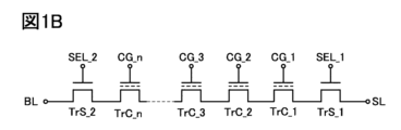
- FIG IB is a circuit diagram of the memory string
- FIG. 2 is a perspective view illustrating a memory block
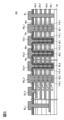
- FIG. 3 is a cross-sectional view illustrating a memory block.
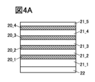
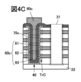
- 4A to 4D are diagrams for explaining a method for manufacturing a memory block
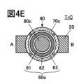
- Fig. 4E is a cross-sectional view for explaining a cell transistor
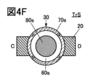
- Fig. 4F is a cross-sectional view for explaining a selection transistor.
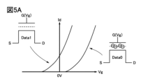
- Fig. 5A is a diagram illustrating the Id-Vg characteristics of a transistor
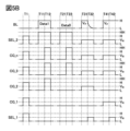
- Fig. 5B is a timing chart illustrating the operation of a memory string.
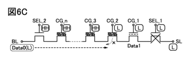
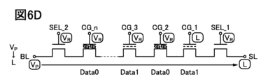
- 6A to 6E are diagrams illustrating the operation of a memory string.
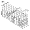
- FIG. 7A is a perspective view illustrating the memory device
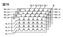
- FIG 7B is a circuit diagram illustrating the memory device.
- FIG. 8 is a block diagram illustrating an example of the configuration of a semiconductor device.
- FIG. 9 is a diagram illustrating an example of the configuration of a semiconductor device.
- FIG. 10 is a block diagram illustrating the CPU.
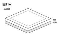
- 11A and 11B are perspective views of a semiconductor device.
- 12A and 12B are perspective views of a semiconductor device.
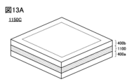
- 13A and 13B are perspective views of a semiconductor device.
- 14A and 14B are diagrams showing various storage devices by hierarchical level.
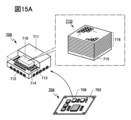
- 15A and 15B are diagrams illustrating an example of an electronic component.
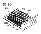
- 16A and 16B are diagrams for explaining an example of an electronic device
- Fig. 16C to Fig. 16E are diagrams for explaining an example of a mainframe computer.
- FIG. 17 is a diagram illustrating an example of space equipment.
- FIG. 18 is a diagram illustrating an example of
- an oxynitride is a material whose composition contains more oxygen than nitrogen.
- examples of oxynitrides include silicon oxynitride, aluminum oxynitride, and hafnium oxynitride.
- a nitride oxide is a material whose composition contains more nitrogen than oxygen. Examples of nitride oxides include silicon nitride oxide, aluminum nitride oxide, and hafnium nitride oxide.
- parallel refers to a state in which two straight lines are arranged at an angle of -10 degrees or more and 10 degrees or less. Therefore, it also includes the case of -5 degrees or more and 5 degrees or less.
- Approximately parallel refers to a state in which two straight lines are arranged at an angle of -30 degrees or more and 30 degrees or less.
- Perfect refers to a state in which two straight lines are arranged at an angle of 80 degrees or more and 100 degrees or less. Therefore, it also includes the case of 85 degrees or more and 95 degrees or less.
- approximately perpendicular refers to a state in which two straight lines are arranged at an angle of 60 degrees or more and 120 degrees or less.
- orthogonal refers to a state in which two straight lines cross or connect at an angle of 80 degrees or more and 100 degrees or less. Therefore, it also includes the case of 85 degrees or more and 95 degrees or less. "Approximately perpendicular” or “approximately perpendicular” refers to a state in which two straight lines cross or connect at an angle of 60 degrees or more and 120 degrees or less.
- arrows indicating the X direction, Y direction, and Z direction may be used.
- the "X direction” is the direction along the X axis, and there may be no distinction between the forward direction and the reverse direction unless explicitly stated. The same applies to the "Y direction” and "Z direction.”
- the X direction, Y direction, and Z direction are directions that intersect with each other.
- the X direction, Y direction, and Z direction are directions that are perpendicular to each other.
- wiring CG (wirings CG_1 to CG_n) are electrically connected to the gates of each cell transistor TrC.
- the wiring CG is a wiring that supplies a signal potential for selecting one cell transistor TrC when resetting, writing, and reading data.
- memory strings 10 memory strings 10_1 to 10_4
- the memory strings 10 can also be stacked in 100 or more layers, or in 200 or more layers. The greater the number of stacked memory strings 10, the greater the memory capacity can be.
- each memory string 10 shares structures 30 and 40. Therefore, by forming an alternating stack of insulators and conductors 20 (conductors 20_1 to 20_4) and then forming structures 30 or 40 at positions that divide the conductors 20, it is possible to form multiple transistors in the height direction using the same material in the same process. In addition, since there is no need to separate structures between upper and lower memory strings, the degree of integration can be increased.
- the memory strings 10 operate in parallel, so the wiring SEL_1, wiring CG, wiring SEL_2, and source line SL can be shared. Since each memory string 10 handles different data, a bit line BL is provided for each memory string 10.
- memory string 10_1 can be electrically connected to bit line BL_1 via conductor 20_1 and plug 50.
- Memory string 10_2 can be electrically connected to bit line BL_2 via conductor 20_2 and plug 50.
- Memory string 10_3 can be electrically connected to bit line BL_3 via conductor 20_3 and plug 50.
- Memory string 10_4 can be electrically connected to bit line BL_4 via conductor 20_4 and plug 50.
- conductors 20_1 to 20_4 can be electrically connected to source line SL via plug 50.
- the conductors 20_1 to 20_4 may be referred to as local bit lines, and the bit lines BL_1 to BL_4 may be referred to as global bit lines.
- FIG. 3 is a cross-sectional view of the memory block 101 shown in FIG. 2.
- the plug and the wiring can be formed separately.
- the conductor 80 is formed as a part of the wiring (wirings CG_1 to CG_4, wiring SEL_1, or wiring SEL_2) is shown, but the conductor 80 and the wiring can be formed separately.
- the oxide semiconductor 70 provided in the structure 30 is illustrated as the oxide semiconductor 70s
- the insulator 60 is illustrated as the insulator 60s.
- the oxide semiconductor 70 provided in the structure 40 is illustrated as the oxide semiconductor 70c
- the insulator 60 is illustrated as the insulator 60c.
- FIGs 4A to 4D are diagrams explaining a method for fabricating the cell transistor TrC and the selection transistor TrS shown in Figure 3.
- a laminate is formed in which insulators 21 (insulators 21_1 to 21_5) and conductors 20 (conductors 20_1 to 20_4) are alternately formed on an insulator 22 (see Figure 4A).
- an oxide semiconductor 70c is formed so as to cover the side and bottom surfaces of the opening 41, and an insulator 60c having a charge storage layer is formed on the oxide semiconductor 70c.
- a conductor 80c is formed on the insulator 60c so as to fill the opening 41 (see FIG. 4C). At this point, the multiple cell transistors TrC shown in FIG. 3 are completed.
- an opening 31 that is circular in top view and reaches the insulator 22 is formed (see FIG. 4C). Note that, although an example is shown in which the opening 41 and the opening 31 have the same diameter, this is not limiting and can be set as appropriate.
- an oxide semiconductor 70s is formed so as to cover the side and bottom surfaces of the opening 41, and an insulator 60s is formed on the oxide semiconductor 70s.
- the oxide semiconductor 70s may be formed of the same material as the oxide semiconductor 70c.
- a conductor 80s is formed on the insulator 60s so as to fill the opening 31 (see FIG. 4D). At this point, the selection transistors TrS_1 and TrS_2 shown in FIG. 3 are completed.
- openings are formed for forming the source lines SL and bit lines BL, and the source lines SL and bit lines BL are formed so as to fill the openings (see FIG. 3).
- the selection transistors TrS_1 and TrS_2 can be manufactured in the same process, so that the number of transistor manufacturing steps can be reduced compared to the conventional 3D NAND manufacturing process. Note that, although an example in which structure 30 is formed after structure 40 is formed has been shown above, structure 40 may also be formed after structure 30 is formed.
- Figure 4E is a cross-sectional view of the cell transistor TrC at the position A-B shown in Figure 4D.
- the cell transistor TrC has an oxide semiconductor 70c on the side (outermost periphery) of the structure 40, an insulator 60c on the inside thereof, and a conductor 80c further inside.
- the oxide semiconductor 70c, the insulator 60c, and the conductor 80c are arranged concentrically.
- One of the conductors 20 is provided in contact with a first region that is part of the side of the oxide semiconductor 70c, and the other of the conductors 20 is provided in contact with a second region opposite the first region.
- the other of the conductors 20 acts as a drain electrode.
- the conductor 20 is provided with a width smaller than the diameter of the structure 40. Therefore, the region of the oxide semiconductor 70c in contact with one of the conductors 20 functions as one of the source and drain, and the region of the oxide semiconductor 70c in contact with the other of the conductors 20 functions as the other of the source and drain. In addition, between the one and the other of the conductors 20, the region of the oxide semiconductor 70c that is not in contact with the one or the other of the conductors 20 functions as a channel formation region.
- the oxide semiconductor 70c Since the oxide semiconductor 70c has a ring shape, there are two channel formation regions between one side of the conductor 20 and the other side.
- the channel length of the cell transistor TrC corresponds to the distance on the circumference of the oxide semiconductor 70c between one side of the conductor 20 and the other side (see the dashed arrow in the figure), and the channel width corresponds to the thickness of the conductor 20.
- the channel length can be controlled by the diameter of the structure 40 (diameter of the opening 41). For example, if it is desired to increase the channel length, the diameter of the structure 40 can be increased. Alternatively, it can be controlled by the width of the conductor 20.
- the opening is circular when viewed from above has been shown, one embodiment of the present invention is not limited to this.
- the opening can be circular when viewed from above, as well as elliptical, polygonal with rounded corners, etc. Note that the circular shape is not limited to a perfect circle.
- the insulator 60c functions as a gate insulator and a memory region.
- the conductor 80c functions as a gate electrode. That is, the conductor 80c functions as a control gate of the memory cell.
- the insulator 61 constituting the insulator 60c functions as a block layer, the insulator 62 functions as a charge storage layer, and the insulator 63 functions as a tunnel layer. When a high voltage is applied to the conductor 80c, electrons can be injected from the oxide semiconductor 70c through the insulator 63 into the insulator 62.
- the gate of the cell transistor TrC is electrically connected to the wiring CG. That is, the conductor 80c is electrically connected to the wiring CG. Alternatively, as shown in FIG. 3, the conductor 80c may be formed as part of the wiring CG.
- the wiring CG can also be called the "control gate” or "control gate wiring.”
- the insulator 62 which functions as a charge storage layer, is made of a material having a smaller band gap than the insulators 61 and 63.
- the thickness of the insulator 63 (length in a direction perpendicular to the Z direction) is preferably 1 nm or more and 10 nm or less.
- the thickness of the insulator 62 is preferably 5 nm or more and 20 nm or less.
- the thickness of the insulator 61 is preferably 5 nm or more and 50 nm or less.
- the thickness of the insulator 63 is preferably thinner than the insulator 61.
- silicon oxide can be used for insulators 61 and 63
- silicon nitride can be used for insulator 62.
- Insulators 61 to 63 can each have a layered structure of multiple insulators.
- insulator 63 can have a layered structure of silicon oxide and aluminum oxide. By making insulator 63 have a layered structure, the reliability of the cell transistor TrC can be improved.
- silicon nitride can be used for the insulators 61 and 63.
- the insulator 62 can function as a charge storage layer.
- Figure 4F is a cross-sectional view of the select transistor TrS at the position C-D shown in Figure 4D.
- the select transistor TrS differs from the cell transistor TrC in that it does not have a charge storage layer.
- the selection transistor TrS has an oxide semiconductor 70s on the side (outermost periphery) of the structure 30, an insulator 60s inside that, and a conductor 80s inside that.
- the oxide semiconductor 70s, the insulator 60s, and the conductor 80s are arranged concentrically.
- One of the conductors 20 is provided in contact with a first region that is part of the side of the oxide semiconductor 70s, and the other of the conductors 20 is provided in contact with a second region opposite the first region.
- the other of the conductors 20 acts as a drain electrode.
- the insulator 60s functions as a gate insulator.
- the insulator 60s can be made of silicon oxide.
- the conductor 80s functions as a gate electrode.
- the cell transistor TrC and the selection transistor TrS are transistors (also referred to as "OS transistors") that use an oxide semiconductor (oxide semiconductors 70c and 70s), which is a type of metal oxide, in a semiconductor layer in which a channel is formed.
- oxide semiconductors 70c and 70s oxide semiconductors 70c and 70s
- the off-current of an oxide semiconductor is extremely small because the band gap of the oxide semiconductor is 2 eV or more. This allows the power consumption of the memory string 10 to be reduced. This allows the power consumption of a storage device including the memory string 10 to be reduced.
- transistors using polycrystalline silicon exhibit variations in threshold voltage due to grain boundaries, but OS transistors are less affected by grain boundaries and have small variations in threshold voltage. Therefore, by using OS transistors for the cell transistors TrC, the memory string 10 can suppress malfunctions caused by variations in threshold voltage.
- the substrate on which the memory string 10 is formed may be, for example, an insulating substrate, a semiconductor substrate, or a conductive substrate.
- insulating substrates include glass substrates, quartz substrates, sapphire substrates, stabilized zirconia substrates (such as yttria-stabilized zirconia substrates), and resin substrates.
- semiconductor substrates include semiconductor substrates made of silicon or germanium, or compound semiconductor substrates made of silicon carbide, silicon germanium, gallium arsenide, indium phosphide, zinc oxide, and gallium oxide.
- semiconductor substrates include semiconductor substrates having an insulator region inside the aforementioned semiconductor substrate, such as an SOI (Silicon On Insulator) substrate.
- Examples of materials with a high dielectric constant include aluminum oxide, gallium oxide, hafnium oxide, tantalum oxide, zirconium oxide, hafnium zirconium oxide, oxides having aluminum and hafnium, oxynitrides having aluminum and hafnium, oxides having silicon and hafnium, oxynitrides having silicon and hafnium, and nitrides having silicon and hafnium.
- materials with a low relative dielectric constant include inorganic insulating materials such as silicon oxide, silicon oxynitride, and silicon nitride oxide, and resins such as polyester, polyolefin, polyamide (nylon, aramid, etc.), polyimide, polycarbonate, and acrylic.
- inorganic insulating materials with a low relative dielectric constant include silicon oxide with added fluorine, silicon oxide with added carbon, and silicon oxide with added carbon and nitrogen. Another example is silicon oxide with vacancies. These silicon oxides may contain nitrogen.
- the electrical characteristics of a transistor using a metal oxide (oxide semiconductor) can be stabilized by surrounding it with an insulator that has a function of suppressing the permeation of impurities and oxygen.
- an insulator that has a function of suppressing the permeation of impurities and oxygen for example, an insulator containing boron, carbon, nitrogen, oxygen, fluorine, magnesium, aluminum, silicon, phosphorus, chlorine, argon, gallium, germanium, yttrium, zirconium, lanthanum, neodymium, hafnium, or tantalum can be used in a single layer or a stacked layer.
- metal oxides such as aluminum oxide, magnesium oxide, gallium oxide, germanium oxide, yttrium oxide, zirconium oxide, lanthanum oxide, neodymium oxide, hafnium oxide, and tantalum oxide
- metal nitrides such as aluminum nitride, silicon nitride oxide, and silicon nitride can be used.
- Insulators in contact with a semiconductor such as a gate insulator, or insulators provided near a semiconductor layer are preferably insulators having a region containing excess oxygen.
- insulators having a region containing excess oxygen in contact with a semiconductor layer or in the vicinity of the semiconductor layer, oxygen vacancies in the semiconductor layer can be reduced.
- Examples of insulators that are likely to form a region containing excess oxygen include silicon oxide, silicon oxynitride, and silicon oxide with vacancies.
- Insulators that have a barrier property against oxygen include oxides containing either or both of aluminum and hafnium, oxides containing hafnium and silicon (hafnium silicate), magnesium oxide, gallium oxide, silicon nitride, and silicon nitride oxide.
- oxides containing either or both of aluminum and hafnium include aluminum oxide, hafnium oxide, and oxides containing aluminum and hafnium (hafnium aluminate).
- Insulators that have barrier properties against hydrogen include aluminum oxide, magnesium oxide, hafnium oxide, gallium oxide, silicon nitride, and silicon nitride oxide.
- An insulator that has a barrier property against oxygen and an insulator that has a barrier property against hydrogen can be said to have a barrier property against either or both of oxygen and hydrogen.
- Insulators having the function of capturing or fixing hydrogen include oxides containing magnesium, or oxides containing one or both of aluminum and hafnium. It is more preferable that these oxides have an amorphous structure. In oxides having an amorphous structure, oxygen atoms have dangling bonds, and the dangling bonds may have the property of capturing or fixing hydrogen. It is preferable that these oxides have an amorphous structure, but crystalline regions may be formed in some parts.
- a barrier insulating film refers to an insulating film having a barrier property.
- the barrier property refers to a property that a corresponding substance is difficult to diffuse (also referred to as a property that a corresponding substance is difficult to permeate, a property that the permeability of a corresponding substance is low, or a function of suppressing the diffusion of a corresponding substance).
- the function of capturing or fixing a corresponding substance can be rephrased as a barrier property.
- hydrogen refers to at least one of, for example, a hydrogen atom, a hydrogen molecule, and a substance bonded to hydrogen such as a water molecule and OH ⁇ .
- impurities refer to impurities in a channel formation region or a semiconductor layer unless otherwise specified, and refer to at least one of, for example, a hydrogen atom, a hydrogen molecule, a water molecule, a nitrogen atom, a nitrogen molecule, a nitrogen oxide molecule (N 2 O, NO, NO 2, etc.), a copper atom, etc.
- oxygen refers to at least one of, for example, an oxygen atom, an oxygen molecule, etc.
- the barrier property against oxygen refers to a property that at least one of an oxygen atom, an oxygen molecule, etc. is difficult to diffuse.
- the conductor it is preferable to use a metal element selected from aluminum, chromium, copper, silver, gold, platinum, tantalum, nickel, titanium, molybdenum, tungsten, hafnium, vanadium, niobium, manganese, magnesium, zirconium, beryllium, indium, ruthenium, iridium, strontium, lanthanum, etc., or an alloy containing the above-mentioned metal elements as a component, or an alloy combining the above-mentioned metal elements.
- a nitride of the alloy or an oxide of the alloy may be used as the alloy containing the above-mentioned metal elements as a component.
- tantalum nitride titanium nitride, tungsten, a nitride containing titanium and aluminum, a nitride containing tantalum and aluminum, ruthenium oxide, ruthenium nitride, an oxide containing strontium and ruthenium, an oxide containing lanthanum and nickel, etc.
- a semiconductor with high electrical conductivity typified by polycrystalline silicon containing an impurity element such as phosphorus, or a silicide such as nickel silicide may be used.
- conductive materials containing nitrogen such as nitrides containing tantalum, nitrides containing titanium, nitrides containing molybdenum, nitrides containing tungsten, nitrides containing ruthenium, nitrides containing tantalum and aluminum, or nitrides containing titanium and aluminum
- conductive materials containing oxygen such as ruthenium oxide, oxides containing strontium and ruthenium, or oxides containing lanthanum and nickel
- materials containing metal elements such as titanium, tantalum, or ruthenium are preferred because they are conductive materials that are difficult to oxidize, conductive materials that have a function of suppressing the diffusion of oxygen, or materials that maintain conductivity even when oxygen is absorbed.
- examples of conductive materials containing oxygen include indium oxide containing tungsten oxide, indium oxide containing titanium oxide, indium tin oxide, indium tin oxide containing titanium oxide, indium tin oxide to which silicon has been added, indium zinc oxide, and indium zinc oxide containing tungsten oxide.
- a conductive film formed using a conductive material containing oxygen may be called an oxide conductive film.
- conductive materials primarily composed of tungsten, copper, or aluminum are preferred because they have high conductivity.
- multiple conductive layers formed from the above materials can be stacked and used.
- a stacked structure can be used that combines the above-mentioned material containing a metal element with a conductive material containing oxygen.
- a stacked structure can be used that combines the above-mentioned material containing a metal element with a conductive material containing nitrogen.
- a stacked structure can be used that combines the above-mentioned material containing a metal element with a conductive material containing oxygen and a conductive material containing nitrogen.
- a conductive material containing oxygen and a metal element contained in the metal oxide in which the channel is formed as a conductor that functions as a gate electrode may also be used.
- a conductive material containing the above-mentioned metal element and nitrogen may also be used.
- a conductive material containing nitrogen such as titanium nitride or tantalum nitride, may be used.
- Indium tin oxide, indium oxide containing tungsten oxide, indium zinc oxide containing tungsten oxide, indium oxide containing titanium oxide, indium tin oxide containing titanium oxide, indium zinc oxide, and indium tin oxide with added silicon may also be used.
- Indium gallium zinc oxide containing nitrogen may also be used.
- Non-single crystal structures include, for example, CAAC structures, polycrystalline structures, nc structures, pseudo-amorphous (a-like) structures, and amorphous structures.
- the a-like structure has a structure between the nc structure and the amorphous structure. The classification of crystal structures will be described later.
- metal oxides having an a-like structure and metal oxides having an amorphous structure have voids or low-density regions. That is, metal oxides having an a-like structure and metal oxides having an amorphous structure have lower crystallinity than metal oxides having an nc structure and metal oxides having a CAAC structure. In addition, metal oxides having an a-like structure have a higher hydrogen concentration in the metal oxide than metal oxides having an nc structure and metal oxides having a CAAC structure. Therefore, lattice defects are easily generated in metal oxides having an a-like structure and metal oxides having an amorphous structure.
- a metal oxide with high crystallinity for the semiconductor layer of a transistor.
- a metal oxide having a CAAC structure or a metal oxide having a single crystal structure By using such a metal oxide for a transistor, a transistor with good electrical characteristics can be realized. In addition, a highly reliable transistor can be realized.
- a metal oxide for the channel formation region of a transistor, which increases the on-state current of the transistor.
- the crystal it is preferable to use a metal oxide with high crystallinity for the metal oxide including the channel formation region. Furthermore, it is preferable for the crystal to have a crystal structure in which multiple layers (for example, a first layer, a second layer, and a third layer) are stacked. That is, the crystal has a layered crystal structure (also called a layered crystal or layered structure). In this case, the c-axis of the crystal is oriented in the direction in which the multiple layers are stacked.
- Examples of metal oxides having the crystal include single crystal oxide semiconductors and CAAC-OS (c-axis aligned crystalline oxide semiconductors).
- the c-axis of the crystal in the normal direction to the surface on which the metal oxide is formed or the film surface. This allows the multiple layers to be arranged parallel or approximately parallel to the surface on which the metal oxide is formed or the film surface. In other words, the multiple layers extend in the channel length direction.
- the above three-layered crystal structure has the following structure.
- the first layer has an atomic coordination structure of an oxygen octahedron with the metal of the first layer at the center.
- the second layer has an atomic coordination structure of an oxygen trigonal bipyramid or tetrahedron with the metal of the second layer at the center.
- the third layer has an atomic coordination structure of an oxygen trigonal bipyramid or tetrahedron with the metal of the third layer at the center.
- Examples of the crystal structure of the above crystal include a YbFe 2 O 4 type structure, a Yb 2 Fe 3 O 7 type structure, and modified structures thereof.
- each of the first layer to the third layer is preferably composed of one metal element or multiple metal elements having the same valence, and oxygen.
- the valence of the one or multiple metal elements constituting the first layer is preferably the same as the valence of the one or multiple metal elements constituting the second layer.
- the first layer and the second layer may have the same metal element.
- the valence of the one or multiple metal elements constituting the first layer is different from the valence of the one or multiple metal elements constituting the third layer.
- the above structure improves the crystallinity of the metal oxide and increases the mobility of the metal oxide. Therefore, by using the metal oxide in the channel formation region of a transistor, the on-state current of the transistor increases, and the electrical characteristics of the transistor can be improved.
- Examples of the metal oxide of one embodiment of the present invention include indium oxide, gallium oxide, and zinc oxide.
- the metal oxide of one embodiment of the present invention preferably contains at least indium (In) or zinc (Zn).
- the metal oxide preferably has two or three elements selected from indium, element M, and zinc.
- the element M is a metal element or semimetal element having a high bond energy with oxygen, for example, a metal element or semimetal element having a higher bond energy with oxygen than indium.
- the element M include aluminum, gallium, tin, yttrium, titanium, vanadium, chromium, manganese, iron, cobalt, nickel, zirconium, molybdenum, hafnium, tantalum, tungsten, lanthanum, cerium, neodymium, magnesium, calcium, strontium, barium, boron, silicon, germanium, and antimony.
- the element M in the metal oxide is preferably one or more of the above elements, more preferably one or more selected from aluminum, gallium, tin, and yttrium, and even more preferably gallium.
- the metal oxide of one embodiment of the present invention preferably has one or more selected from indium, gallium, and zinc.
- metal elements and metalloid elements may be collectively referred to as “metal elements", and the "metal element” described in this specification and the like may include metalloid elements.
- indium zinc oxide In-Zn oxide
- indium tin oxide In-Sn oxide
- indium titanium oxide In-Ti oxide
- indium gallium oxide In-Ga oxide
- indium gallium aluminum oxide In-Ga-Al oxide
- indium gallium tin oxide In-Ga-Sn oxide
- gallium zinc oxide Ga-Zn oxide, also referred to as GZO
- aluminum zinc oxide Al-Zn oxide, also referred to as AZO
- IAZO indium Indium aluminum zinc oxide
- indium tin zinc oxide In-Sn-Zn oxide
- indium titanium zinc oxide In-Ti-Zn oxide
- indium gallium tin zinc oxide In-Ga-Sn-Zn oxide, also written as IGZTO
- the field effect mobility of the transistor can be increased.
- the metal oxide may have one or more metal elements with a large periodic number instead of indium.
- the metal oxide may have one or more metal elements with a large periodic number in addition to indium.
- Examples of metal elements with a large periodic number include metal elements belonging to the fifth period and metal elements belonging to the sixth period.
- the metal elements include yttrium, zirconium, silver, cadmium, tin, antimony, barium, lead, bismuth, lanthanum, cerium, praseodymium, neodymium, promethium, samarium, and europium. Note that lanthanum, cerium, praseodymium, neodymium, promethium, samarium, and europium are called light rare earth elements.
- the metal oxide may also contain one or more nonmetallic elements.
- the field effect mobility of the transistor may be increased.
- nonmetallic elements include carbon, nitrogen, phosphorus, sulfur, selenium, fluorine, chlorine, bromine, and hydrogen.
- the metal oxide becomes highly crystalline, and the diffusion of impurities in the metal oxide can be suppressed. Therefore, fluctuations in the electrical characteristics of the transistor can be suppressed, and reliability can be improved.
- the transistor can obtain a large on-current and high frequency characteristics.
- In-Ga-Zn oxide may be used as an example of a metal oxide.
- the metal oxide film formation method of the present invention it is preferable to deposit atoms one layer at a time.
- the ALD method is used, so that it is easy to form a metal oxide having the above-mentioned layered crystal structure.
- ALD plasma Enhanced ALD
- the ALD method can deposit atoms one layer at a time, and therefore has the following advantages: extremely thin films can be formed; films can be formed on structures with high aspect ratios; films can be formed with fewer defects such as pinholes; films can be formed with excellent coverage; and films can be formed at low temperatures.
- the PEALD method may be preferable because it can form films at lower temperatures by using plasma.
- some precursors used in the ALD method contain elements such as carbon or chlorine.
- films formed by the ALD method may contain more elements such as carbon or chlorine than films formed by other film formation methods. Note that the quantification of these elements can be performed using XPS or SIMS.
- the metal oxide film formation method of one embodiment of the present invention uses the ALD method, but adopts one or both of the conditions of a high substrate temperature during film formation and the implementation of an impurity removal process, and therefore the amount of carbon and chlorine contained in the film may be smaller than when the ALD method is used without applying these.
- the ALD method is a film formation method in which a film is formed by a reaction on the surface of a workpiece, unlike a film formation method in which particles released from a target are deposited. Therefore, it is a film formation method that is not easily affected by the shape of the workpiece and has good step coverage.
- the ALD method has excellent step coverage and excellent thickness uniformity, making it suitable for coating the surface of an opening with a high aspect ratio.
- the ALD method since the ALD method has a relatively slow film formation speed, it may be preferable to use it in combination with other film formation methods such as a sputtering method or a CVD method, which have a fast film formation speed.
- a method of forming a first metal oxide film using a sputtering method and forming a second metal oxide film on the first metal oxide using an ALD method can be mentioned.
- the second metal oxide may grow as a crystal using the crystalline portion as a nucleus.
- the ALD method can control the composition of the resulting film by the amount of raw material gas introduced.
- the ALD method can form a film of any composition by adjusting the amount of raw material gas introduced, the number of introductions (also called the number of pulses), the time required for one pulse (also called the pulse time), and the like.
- the ALD method can form a film whose composition changes continuously by changing the raw material gas while forming the film.
- the time required for film formation can be shortened compared to forming a film using multiple film formation chambers because no time is required for transportation and pressure adjustment. Therefore, the productivity of memory devices can be increased in some cases.
- Lattice defects include point defects such as atomic vacancies and foreign atoms, line defects such as dislocations, surface defects such as grain boundaries, and volume defects such as voids.
- Factors that cause lattice defects include a discrepancy in the ratio of the atomic numbers of the constituent elements (an excess or deficiency of constituent atoms) and impurities.
- the metal oxide used in the semiconductor layer of a transistor When a metal oxide is used in the semiconductor layer of a transistor, lattice defects in the metal oxide can cause carrier generation or capture. Therefore, if a metal oxide with many lattice defects is used in the semiconductor layer of a transistor, the electrical characteristics of the transistor may become unstable. Therefore, it is preferable that the metal oxide used in the semiconductor layer of a transistor has few lattice defects.
- V O H oxygen vacancies
- the transistor is likely to have normally-on characteristics. Therefore, it is preferable that oxygen vacancies and impurities are reduced as much as possible in the channel formation region in the metal oxide. In other words, it is preferable that the carrier concentration of the channel formation region in the metal oxide is reduced and the channel formation region in the metal oxide is made i-type (intrinsic) or substantially i-type.
- the types of lattice defects likely to exist in metal oxides and the amount of lattice defects present vary depending on the structure of the metal oxide or the method of forming the metal oxide film.
- a transistor with high field-effect mobility can be realized.
- a highly reliable transistor can be realized.
- a miniaturized or highly integrated transistor can be realized. For example, a transistor with a channel length of 2 nm to 30 nm can be manufactured.
- an oxide semiconductor having a low carrier concentration is preferably used for the channel formation region of the transistor.
- the carrier concentration of the channel formation region of the oxide semiconductor is 1 ⁇ 10 18 cm ⁇ 3 or less, preferably 1 ⁇ 10 17 cm ⁇ 3 or less, more preferably 1 ⁇ 10 15 cm ⁇ 3 or less, more preferably 1 ⁇ 10 13 cm ⁇ 3 or less, more preferably 1 ⁇ 10 11 cm ⁇ 3 or less, and further preferably less than 1 ⁇ 10 10 cm ⁇ 3 and 1 ⁇ 10 ⁇ 9 cm ⁇ 3 or more. Note that in order to reduce the carrier concentration of the oxide semiconductor, it is only necessary to reduce the impurity concentration in the oxide semiconductor and reduce the density of defect states.
- a semiconductor having a low impurity concentration and a low density of defect states is referred to as a high-purity intrinsic or substantially high-purity intrinsic.
- an oxide semiconductor having a low carrier concentration may be referred to as a high-purity intrinsic or substantially high-purity intrinsic oxide semiconductor.
- a highly pure intrinsic or substantially highly pure intrinsic oxide semiconductor film has a low density of defect states, and therefore may also have a low density of trap states.
- the charge trapped in the trap states of the oxide semiconductor takes a long time to disappear and may behave as if it were a fixed charge. Therefore, a transistor in which a channel formation region is formed in an oxide semiconductor with a high density of trap states may have unstable electrical characteristics.
- an impurity in an oxide semiconductor refers to, for example, anything other than the main component that constitutes the oxide semiconductor.
- an element with a concentration of less than 0.1 atomic % can be considered an impurity.
- the band gap of the oxide semiconductor is preferably larger than that of silicon (typically 1.1 eV), and is preferably 2 eV or more, more preferably 2.5 eV or more, and further preferably 3.0 eV or more.
- the off-state current (also referred to as Ioff) of the transistor can be reduced.
- OS transistors use oxide semiconductors, which are semiconductor materials with a wide band gap, and therefore the short channel effect can be suppressed. In other words, OS transistors are transistors that do not have the short channel effect or have an extremely small short channel effect.
- the short channel effect is a degradation of electrical characteristics that becomes evident as transistors are miniaturized (reduced channel length).
- Specific examples of short channel effects include a decrease in threshold voltage, an increase in subthreshold swing value (sometimes referred to as S value), and an increase in leakage current.
- S value refers to the amount of change in gate voltage in the subthreshold region that changes the drain current by one order of magnitude at a constant drain voltage.
- characteristic length is widely used as an index of resistance to short channel effects.
- Characteristic length is an index of how easily the potential of the channel formation region bends. The smaller the characteristic length, the steeper the potential rises, and therefore the more resistant it is to short channel effects.
- OS transistors are accumulation-type transistors, while Si transistors are inversion-type transistors. Therefore, compared to Si transistors, OS transistors have smaller characteristic lengths between the source region and the channel-forming region, and between the drain region and the channel-forming region. Therefore, OS transistors are more resistant to the short-channel effect than Si transistors. In other words, when it is desired to manufacture a transistor with a short channel length, OS transistors are more suitable than Si transistors.
- the OS transistor can also be regarded as having an n + /n ⁇ /n + accumulation-type junction-less transistor structure or an n + /n ⁇ / n + accumulation-type non-junction transistor structure in which the channel formation region is an n ⁇ type region and the source and drain regions are n + type regions.
- the OS transistor can have good electrical characteristics even when the memory device is miniaturized or highly integrated. For example, good electrical characteristics can be obtained even when the channel length or gate length of the OS transistor is 20 nm or less, 15 nm or less, 10 nm or less, 7 nm or less, or 6 nm or less, and 1 nm or more, 3 nm or more, or 5 nm or more.
- the gate length is the length of the gate electrode in the direction in which carriers move inside the channel formation region when the transistor is operating.
- the cutoff frequency of the transistor can be improved.
- the cutoff frequency of the transistor can be set to, for example, 50 GHz or more, preferably 100 GHz or more, and more preferably 150 GHz or more in a room temperature environment.
- OS transistors As explained above, compared to Si transistors, OS transistors have the excellent advantages of having a smaller off-state current and being able to fabricate transistors with a short channel length.
- the carbon concentration in a channel formation region of the oxide semiconductor measured by SIMS is 1 ⁇ 10 20 atoms/cm 3 or less, preferably 5 ⁇ 10 19 atoms/cm 3 or less, more preferably 3 ⁇ 10 19 atoms/cm 3 or less, more preferably 1 ⁇ 10 19 atoms/cm 3 or less, more preferably 3 ⁇ 10 18 atoms/cm 3 or less, and further preferably 1 ⁇ 10 18 atoms/cm 3 or less.
- the silicon concentration in the channel formation region of the oxide semiconductor measured by SIMS is 1 ⁇ 10 20 atoms/cm 3 or less, preferably 5 ⁇ 10 19 atoms/cm 3 or less, more preferably 3 ⁇ 10 19 atoms/cm 3 or less, more preferably 1 ⁇ 10 19 atoms/cm 3 or less, more preferably 3 ⁇ 10 18 atoms/cm 3 or less, and still more preferably 1 ⁇ 10 18 atoms/cm 3 or less.
- the nitrogen concentration in a channel formation region of an oxide semiconductor obtained by SIMS is set to 1 ⁇ 10 20 atoms/cm 3 or less, preferably 5 ⁇ 10 19 atoms/cm 3 or less, more preferably 1 ⁇ 10 19 atoms/cm 3 or less, more preferably 5 ⁇ 10 18 atoms/cm 3 or less, more preferably 1 ⁇ 10 18 atoms/cm 3 or less, and further preferably 5 ⁇ 10 17 atoms/cm 3 or less.
- Hydrogen contained in the oxide semiconductor reacts with oxygen bonded to a metal atom to form water, which may form an oxygen vacancy.
- an electron serving as a carrier may be generated.
- some of the hydrogen may bond to oxygen bonded to a metal atom to generate an electron serving as a carrier. Therefore, a transistor using an oxide semiconductor containing hydrogen is likely to have normally-on characteristics. For this reason, it is preferable that hydrogen in a channel formation region of the oxide semiconductor is reduced as much as possible.
- the hydrogen concentration in the channel formation region of the oxide semiconductor obtained by SIMS is less than 1 ⁇ 10 20 atoms/cm 3 , preferably less than 5 ⁇ 10 19 atoms/cm 3 , more preferably less than 1 ⁇ 10 19 atoms/cm 3 , more preferably less than 5 ⁇ 10 18 atoms/cm 3 , and further preferably less than 1 ⁇ 10 18 atoms/cm 3 .
- the concentration of the alkali metal or the alkaline earth metal in a channel formation region of the oxide semiconductor obtained by SIMS is set to 1 ⁇ 10 18 atoms/cm 3 or less, preferably 2 ⁇ 10 16 atoms/cm 3 or less.
- the oxide semiconductor can be rephrased as a semiconductor layer including a channel formation region of a transistor.
- the semiconductor material that can be used for the semiconductor layer is not limited to the above-mentioned metal oxides.
- a semiconductor material having a band gap (a semiconductor material that is not a zero-gap semiconductor) may be used for the semiconductor layer.
- a semiconductor of a single element, a compound semiconductor, or a layered material (also referred to as an atomic layer material, a two-dimensional material, or the like) is preferably used for the semiconductor material.
- layered material is a general term for a group of materials having a layered crystal structure.
- a layered crystal structure is a structure in which layers formed by covalent bonds or ionic bonds are stacked via bonds weaker than covalent bonds or ionic bonds, such as van der Waals forces.
- Layered materials have high electrical conductivity within a unit layer, that is, high two-dimensional electrical conductivity.
- Examples of elemental semiconductors that can be used in the semiconductor material include silicon and germanium.
- Examples of silicon that can be used in the semiconductor layer include single crystal silicon, polycrystalline silicon, microcrystalline silicon, and amorphous silicon.
- An example of polycrystalline silicon is low temperature polysilicon (LTPS).
- Compound semiconductors that can be used for the semiconductor material include silicon carbide, silicon germanium, gallium arsenide, indium phosphide, boron nitride, and boron arsenide.
- the boron nitride that can be used for the semiconductor layer preferably includes an amorphous structure.
- the boron arsenide that can be used for the semiconductor layer preferably includes crystals with a cubic crystal structure.
- Layered materials include graphene, silicene, boron carbonitride, and chalcogenides.
- boron carbonitride carbon atoms, nitrogen atoms, and boron atoms are arranged in a hexagonal lattice structure on a plane.
- Chalcogenides are compounds that contain chalcogen. Chalcogen is a general term for elements that belong to Group 16, and includes oxygen, sulfur, selenium, tellurium, polonium, and livermorium.
- Other examples of chalcogenides include transition metal chalcogenides and Group 13 chalcogenides.
- transition metal chalcogenide that functions as a semiconductor.
- transition metal chalcogenides that can be used as the semiconductor layer include molybdenum sulfide (representatively MoS 2 ), molybdenum selenide (representatively MoSe 2 ), molybdenum tellurium (representatively MoTe 2 ), tungsten sulfide (representatively WS 2 ), tungsten selenide (representatively WSe 2 ), tungsten tellurium (representatively WTe 2 ), hafnium sulfide (representatively HfS 2 ), hafnium selenide (representatively HfSe 2 ), zirconium sulfide (representatively ZrS 2 ), and zirconium selenide (representatively ZrSe 2 ).
- the cell transistor TrC functions as a memory cell. Data is written by injecting charge into the charge storage layer (insulator 62) of the cell transistor TrC.
- the cell transistor TrC When Data0 is written, the cell transistor TrC operates as a normally-off type (enhancement type) transistor, and when Data1 is written, it operates as a normally-on type (depletion type) transistor.
- the selection transistor TrS_1 and the selection transistor TrS_2 always operate as normally-off type (enhancement type) transistors.
- FIG. 5A is a diagram illustrating an example of the Id-Vg characteristics of the cell transistor TrC.
- the horizontal axis of FIG. 5A represents the gate voltage (Vg), and the vertical axis represents the drain current (Id).
- the threshold voltage of the cell transistor TrC is changed by controlling the flow of electrons into and out of the charge storage layer, and data in the memory string is reset, written, and read.
- a low level potential “L”, a read potential “V R “, a high level potential “H”, and a high level potential “HH” can be used, with “L” ⁇ "V R “ ⁇ ”H” ⁇ ”HH".
- a potential “V P " equivalent to "H” is used to precharge the bit line BL.
- the potential of the source line SL is always “L”. For example, 0 V or a GND potential can be used for "L”.
- TrC memory cells
- the potential of the bit line BL is set to "L”
- the potential of the wiring SEL_2 is set to “H”
- the potential of the wirings CG_1 to CG_n is set to “H”
- the potential of the wiring SEL_1 is set to "H”.
- the high-level potential "H” is a potential at which electrons can be input to and output from the charge storage layer and is a potential at which the normally-off transistor can be made conductive.
- the selection transistor TrS_1, the cell transistor TrC, and the selection transistor TrS_2 are conductive.
- the cell transistor TrC electrons are supplied from the semiconductor layer to the charge storage layer through the tunnel layer due to the potential difference between the gate and the source and drain (see FIG. 6A). This operation resets the data in all the cell transistors TrC (memory cells).
- the potential of the bit line BL is set to "Data1”
- the potential of the wiring SEL_2 is set to "HH”
- the potential of the wirings CG_1 to CG_n is set to “L”
- the potential of the wiring SEL_1 is set to "L”.
- “Data1” corresponds to data "1”
- “Data1” can be set to a potential equivalent to a high-level potential “H”.
- the high-level potential "HH” is a potential that can turn on a normally-off transistor whose source potential is "H”.
- the potential of the bit line BL is set to "Data1”
- the potential of the wiring SEL_2 is set to "HH”
- the potential of the wirings CG_2 to CG_n is set to "HH”
- the potential of the wiring CG_1 is set to "L”
- the potential of the wiring SEL_1 is set to "L”.
- the selection transistor TrS_2 and the cell transistors TrC_2 to TrC_n are conductive, and the potential "Data1" of the bit line BL is supplied to either the source or drain of the cell transistor TrC_1.
- the potential difference between the gate and either the source or the drain causes electrons to be emitted from the charge storage layer through the tunnel layer to the semiconductor layer (see FIG. 6B). This state can be said to be writing "Data1" to the cell transistor TrC_1.
- the potential of the bit line BL is set to "Data0”
- the potential of the wiring SEL_2 is set to "HH”
- the potential of the wirings CG_1 to CG_n is set to “L”
- the potential of the wiring SEL_1 is set to "L”.
- “Data0” corresponds to data “0”
- “Data0” can be set to a potential equivalent to the low-level potential “L”.
- the potential of the bit line BL is set to "Data0”
- the potential of the wiring SEL_2 is set to "HH”
- the potential of the wirings CG_3 to CG_n is set to "HH”
- the potentials of the wirings CG_1 and CG_2 are set to "L”
- the potential of the wiring SEL_1 is set to "L”.
- the selection transistor TrS_2 and the cell transistors TrC_3 to TrC_n are conductive, and the potential "Data0" of the bit line BL is supplied to either the source or drain of the cell transistor TrC_2.
- the gate and either the source or the drain are at approximately the same potential, so the electrons supplied during period T1 remain in the charge storage layer (see FIG. 6C). This state can be said to be writing "Data0" to the cell transistor TrC_2.
- a potential of "L” is supplied to the gate of the cell transistor TrC to be read.
- Data1 is written to the cell transistor TrC and the cell transistor TrC is normally on, the transistor is conductive even if the potential supplied to the gate is "L”.
- Data0 is written to the cell transistor TrC and the cell transistor TrC is normally off, the transistor is non-conductive when the potential supplied to the gate is "L”.
- the potential of the bit line BL is set to "V P "
- the potential of the wiring SEL_2 is set to “V R "
- the potential of the wirings CG_2 to CG_n is set to “V R”
- the potential of the wiring CG_1 is set to "L”
- the potential of the wiring SEL_1 is set to "L”.
- the bit line BL is set to a floating state.
- V P is a precharge potential, which can be set to, for example, a potential equivalent to the first high-level potential "H”.
- V R is a read potential, which is a potential equal to or higher than the threshold voltage of a normally-off transistor.
- the selection transistor TrS_2 is turned on. Furthermore, since "Data1" is written to the cell transistor TrC_1 and the cell transistor TrC_1 is a normally-on type, the cell transistor TrC_1 is turned on even when the potential of the wiring CG_1 is "L". Furthermore, the cell transistors TrC_2 to TrC_n are turned on because a voltage "V R " equal to or higher than the threshold voltage is applied to their gates. However, since the selection transistor TrS_1 is turned off, the potential of the bit line BL does not change from "V P ".
- the potential of the wiring SEL_2 is set to "V R "
- the potentials of the wirings CG_2 to CG_n are set to “V R "
- the potential of the wiring CG_1 is set to "L”
- the potential of the wiring SEL_1 is set to "V R ".
- the potential of the bit line BL is set to "V P "
- the potential of the wiring SEL_2 is set to "V R "
- the potential of the wirings CG_3 to CG_n is set to “V R "
- the potential of the wiring CG_2 is set to "L”
- the potential of the wiring CG_1 is set to “V R”
- the potential of the wiring SEL_1 is set to "L”.
- the bit line BL is set to a floating state.
- the selection transistor TrS_2 is turned on. Furthermore, since "Data0" is written to the cell transistor TrC_2 and the cell transistor TrC_2 is a normally-off type, the cell transistor TrC_2 is turned off when the potential of the wiring CG_1 is "L". Furthermore, the cell transistors TrC_1 and TrC_3 to TrC_n are turned on because a voltage "V R " equal to or higher than the threshold voltage is applied to their gates. At this time, since the cell transistor TrC_2 and the selection transistor TrS_1 are turned off, the potential of the bit line BL does not change from "V P ".
- the potential of the wiring SEL_2 is set to "V R "
- the potentials of the wirings CG_3 to CG_n are set to “V R "
- the potential of the wiring CG_2 is set to "L”
- the potential of the wiring CG_1 is set to “V R”
- the potential of the wiring SEL_1 is set to "V R ".
- the selection transistor TrS_1 is conductive, but the cell transistor TrC_2 is non-conductive, so the bit line BL and the source line SL are not conductive, and the potential of the bit line BL, which has been precharged to "V P ", does not change. Therefore, by reading the potential "V P " of the bit line BL with a sense amplifier, "Data0" can be read from the cell transistor TrC_1 (see FIG. 6E).
- wiring SEL_1, wiring CG, and wiring SEL_2 are shared by multiple memory strings, so multiple memory strings can operate in parallel.
- the storage device of one embodiment of the present invention may have a structure including a plurality of memory blocks.
- FIG. 7A is a perspective view illustrating a storage device including memory blocks 101 to 104
- FIG. 7B is a circuit diagram illustrating connections between the memory blocks 101 to 104 and each wiring.
- Memory blocks 101 to 104 can have the same configuration, and Figures 7A and 7B show an example of a configuration in which each memory block has four memory strings (see Figures 2 and 3). Since the number of wirings would be enormous if independent wiring were provided for each memory block, it is preferable to share some wirings among the memory blocks.
- Figures 7A and 7B show an example in which the wiring CG and bit lines BL (bit lines BL_1 to BL_4) are shared by each memory block. Such bit lines BL shared by multiple memory blocks can be called global bit lines.
- bit line BL is shared, data is reset, written, and read for each memory block. Therefore, wiring connecting to the selection transistor TrS is provided for each memory block.
- wiring SEL_1a is electrically connected to selection transistor TrS_1, and wiring SEL_2a is electrically connected to selection transistor TrS_2.
- wiring SEL_1b is electrically connected to selection transistor TrS_1, and wiring SEL_2b is electrically connected to selection transistor TrS_2.
- wiring SEL_1c is electrically connected to selection transistor TrS_1, and wiring SEL_2c is electrically connected to selection transistor TrS_2.
- wiring SEL_1d is electrically connected to selection transistor TrS_1, and wiring SEL_2d is electrically connected to selection transistor TrS_2.
- each memory block may share a selection transistor.
- each memory block may be provided with the same number of bit lines BL as memory strings. Although the number of wirings increases, multiple memory blocks can be operated in parallel, allowing data to be reset, written, and read at high speed.
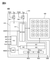
- FIG. 8 shows a block diagram illustrating an example of the configuration of a semiconductor device 400.
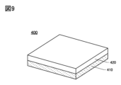
- the semiconductor device 400 shown in FIG. 8 has a drive circuit 410 and a memory array 420.
- the memory array 420 has one or more memory strings 10.
- the drive circuit 410 has a PSW241 (power switch), a PSW242, and a peripheral circuit 415.
- the peripheral circuit 415 has a peripheral circuit 411, a control circuit 412, and a voltage generation circuit 428.
- each circuit, signal, and voltage can be selected or removed as needed. Alternatively, other circuits or signals may be added.
- the signals BW, CE, GW, CLK, WAKE, ADDR, WDA, PON1, and PON2 are input signals from the outside, and the signal RDA is an output signal to the outside.
- the signal CLK is a clock signal.
- signals BW, CE, and GW are control signals.
- Signal CE is a chip enable signal
- signal GW is a global write enable signal
- signal BW is a byte write enable signal.
- Signal ADDR is an address signal.
- Signal WDA is write data
- signal RDA is read data.
- Signals PON1 and PON2 are power gating control signals. Signals PON1 and PON2 may be generated by control circuit 412.
- the control circuit 412 is a logic circuit that has the function of controlling the overall operation of the semiconductor device 400. For example, the control circuit performs a logical operation on the signals CE, GW, and BW to determine the operation mode (e.g., write operation, read operation) of the semiconductor device 400. Alternatively, the control circuit 412 generates a control signal for the peripheral circuit 411 so that this operation mode is executed.
- the control circuit performs a logical operation on the signals CE, GW, and BW to determine the operation mode (e.g., write operation, read operation) of the semiconductor device 400.
- the control circuit 412 generates a control signal for the peripheral circuit 411 so that this operation mode is executed.
- the voltage generation circuit 428 has a function of generating a negative voltage.
- WAKE has a function of controlling the input of CLK to the voltage generation circuit 428. For example, when an H-level signal is given to WAKE, the signal CLK is input to the voltage generation circuit 428, and the voltage generation circuit 428 generates a negative voltage.
- the peripheral circuit 411 is a circuit for writing and reading data to and from the memory string 10.
- the peripheral circuit 411 includes a row decoder 441, a column decoder 442, a row driver 423, a column driver 424, an input circuit 425, an output circuit 426, and a sense amplifier 427.
- the row decoder 441 and the column decoder 442 have the function of decoding the signal ADDR.
- the row decoder 441 is a circuit for specifying the row to be accessed
- the column decoder 442 is a circuit for specifying the column to be accessed.
- the row driver 423 has the function of selecting the wiring CG specified by the row decoder 441.
- the column driver 424 has the function of writing data to the memory string 10, reading data from the memory string 10, and holding the read data.
- the input circuit 425 has a function of holding a signal WDA.
- the data held by the input circuit 425 is output to the column driver 424.
- the output data of the input circuit 425 is data (Din) to be written to the memory string 10.
- the data (Dout) read from the memory string 10 by the column driver 424 is output to the output circuit 426.
- the output circuit 426 has a function of holding Dout.
- the output circuit 426 has a function of outputting Dout to the outside of the semiconductor device 400.
- the data output from the output circuit 426 is the signal RDA.
- the PSW 241 has a function of controlling the supply of V DD to the peripheral circuit 415.
- the PSW 242 has a function of controlling the supply of V HM to the row driver 423.
- the high power supply voltage of the semiconductor device 400 is V DD
- the low power supply voltage is GND (ground potential).
- V HM is a high power supply voltage used to set the word line to a high level, and is higher than V DD .
- the signal PON1 controls the on/off of the PSW 241, and the signal PON2 controls the on/off of the PSW 242.
- the number of power supply domains to which V DD is supplied in the peripheral circuit 415 is one, but it may be more than one. In this case, a power switch may be provided for each power supply domain.
- the driving circuit 410 and memory array 420 of the semiconductor device 400 may be provided on the same plane. Also, as shown in FIG. 9, the driving circuit 410 and memory array 420 may be provided overlapping each other. By providing the driving circuit 410 and memory array 420 overlapping each other, the signal propagation distance can be shortened.
- the semiconductor device 400 may also use an arithmetic processing device such as a CPU (Central Processing Unit) and a GPU (Graphics Processing Unit) in the control circuit 412 of the drive circuit 410.
- an arithmetic processing device such as a CPU (Central Processing Unit) and a GPU (Graphics Processing Unit) in the control circuit 412 of the drive circuit 410.
- a CPU and a GPU etc.
- a semiconductor device 400 having an arithmetic processing function can be realized.
- Memory string 10 can function as a RAM. Therefore, a part of memory array 420 can function as a main memory or a cache memory. Memory string 10 can also function as a flash memory. Therefore, a part of memory array 420 can function like a flash memory.
- the semiconductor device 400 according to one aspect of the present invention can function as a universal memory.
- the functions of a CPU, cache memory, and storage can be realized on the same chip.
- the semiconductor device 400 shown in FIG. 9 has a driver circuit 410 including a CPU, and a 3D OS NAND type storage device according to one embodiment of the present invention in a memory array 420.
- the 3D OS NAND type storage device according to one embodiment of the present invention can function as a cache memory and as a storage device.
- Figure 10 shows a block diagram of the central processing unit 1100.
- Figure 10 shows an example of a CPU configuration that can be used for the central processing unit 1100.
- the central processing unit 1100 shown in FIG. 10 has an ALU 1191 (ALU: Arithmetic logic unit, arithmetic circuit), an ALU controller 1192, an instruction decoder 1193, an interrupt controller 1194, a timing controller 1195, a register 1196, a register controller 1197, a bus interface 1198), a cache 1199, and a cache interface 1189 on a substrate 1190.
- the substrate 1190 is a semiconductor substrate, an SOI substrate, a glass substrate, or the like. It may have a rewritable ROM and a ROM interface.
- the cache 1199 and the cache interface 1189 may be provided on separate chips.
- the cache 1199 is connected to a main memory provided on a separate chip via a cache interface 1189.
- the cache interface 1189 has a function of supplying a portion of the data stored in the main memory to the cache 1199.
- the cache 1199 has a function of storing that data.
- the central processing unit 1100 shown in FIG. 10 is merely one example of a simplified configuration, and an actual central processing unit 1100 has a wide variety of configurations depending on its application.
- the central processing unit 1100 shown in FIG. 10 or a configuration including an arithmetic circuit may be one core, and a configuration including multiple such cores may be configured so that each core operates in parallel, in other words, a configuration similar to a GPU.
- the number of bits that the central processing unit 1100 can handle in the internal arithmetic circuit and data bus may be, for example, 8 bits, 16 bits, 32 bits, 64 bits, etc.
- Instructions input to the central processing unit 1100 via the bus interface 1198 are input to the instruction decoder 1193, decoded, and then input to the ALU controller 1192, the interrupt controller 1194, the register controller 1197, and the timing controller 1195.
- the ALU controller 1192, interrupt controller 1194, register controller 1197, and timing controller 1195 perform various controls based on the decoded instructions. Specifically, the ALU controller 1192 generates signals for controlling the operation of the ALU 1191. Furthermore, while the central processing unit 1100 is executing a program, the interrupt controller 1194 determines and processes interrupt requests from external input/output devices or peripheral circuits based on their priority or mask state. The register controller 1197 generates an address for the register 1196, and reads and writes to the register 1196 depending on the state of the central processing unit 1100.
- the timing controller 1195 also generates signals that control the timing of the operations of the ALU 1191, the ALU controller 1192, the instruction decoder 1193, the interrupt controller 1194, and the register controller 1197.
- the timing controller 1195 includes an internal clock generation unit that generates an internal clock signal based on a reference clock signal, and supplies the internal clock signal to the various circuits described above.
- a memory device is provided in the register 1196 and the cache 1199.
- the memory device for example, the memory device shown in the previous embodiment can be used.
- connection distance between them can be shortened. This allows the communication speed between them to be increased. In addition, the short connection distance allows for reduced power consumption.
- the control circuit 412 can cause some or all of the multiple memory strings 10 of the semiconductor device 400 to function as RAM based on a signal supplied from the central processing unit 1100.
- the semiconductor device 400 can cause some of the multiple memory strings 10 to function as RAM, and the other memory strings 10 to function as storage.
- a 3D OS NAND type storage device for the semiconductor device 400, it can function as a cache, a main memory, and a storage.
- the semiconductor device 400 according to one aspect of the present invention can function as a universal memory, for example.
- the semiconductor device 400 when the semiconductor device 400 is used as a main memory, its storage capacity can be increased or decreased as needed.Furthermore, when the semiconductor device 400 is used as a cache, its storage capacity can be increased or decreased as needed.
- the control circuit 412 may have a function of performing ECC when data is moved or copied between an area functioning as main memory of the semiconductor device 400 and the cache 1199.
- FIGs. 12A and 12B show perspective views of the semiconductor device 1150B.
- the semiconductor device 1150B has a semiconductor device 400a and a semiconductor device 400b on the central processing unit 1100.
- the central processing unit 1100, the semiconductor device 400a, and the semiconductor device 400b have overlapping regions.
- the central processing unit 1100, the semiconductor device 400a, and the semiconductor device 400b are shown separately in Fig. 12B.
- the semiconductor device 400a and the semiconductor device 400b function as memory devices.
- a NOR type memory device may be used for one of the semiconductor device 400a or the semiconductor device 400b, and a NAND type memory device may be used for the other.
- Both the semiconductor device 400a and the semiconductor device 400b may be NAND type memory devices.
- Examples of NOR type memory devices include DRAM and SRAM. Since NOR type memory devices can operate faster than NAND type memory devices, for example, a part of the semiconductor device 400a can be used as a main memory and/or cache 1199. Note that the stacking order of the semiconductor device 400a and the semiconductor device 400b may be reversed.
- FIGS 13A and 13B show perspective views of semiconductor device 1150C.
- Semiconductor device 1150C has a configuration in which central processing unit 1100 is sandwiched between semiconductor device 400a and semiconductor device 400b.
- Central processing unit 1100, semiconductor device 400a, and semiconductor device 400b have overlapping areas.
- central processing unit 1100, semiconductor device 400a, and semiconductor device 400b are shown separately in Figure 13B.
- the semiconductor device 1150C By configuring the semiconductor device 1150C, it is possible to increase the communication speed between the semiconductor device 400a and the central processing unit 1100, and the communication speed between the semiconductor device 400b and the central processing unit 1100. In addition, it is possible to reduce power consumption compared to the semiconductor device 1150B.
- Figure 14A shows various memory devices used in semiconductor devices by layer. The higher the layer, the faster the operating speed is required for the memory device, and the lower the layer, the larger the memory capacity and higher the recording density are required for the memory device. From the top layer, Figure 14A shows memory integrated as a register in a processing unit such as a CPU, SRAM (Static Random Access Memory), DRAM (Dynamic Random Access Memory), and 3D NAND memory.
- a processing unit such as a CPU, SRAM (Static Random Access Memory), DRAM (Dynamic Random Access Memory), and 3D NAND memory.
- Registers also have the function of storing setting information for the processor.
- SRAM is used, for example, in caches.
- Caches have the function of duplicating and storing part of the data stored in main memory. By duplicating frequently used data and storing it in the cache, the speed of accessing the data can be increased.
- the storage capacity required for a cache is smaller than that of main memory, but it is required to operate at a faster speed than main memory.
- data rewritten in the cache is duplicated and supplied to the main memory.
- DRAM is used, for example, as a main memory.
- the main memory has a function of holding programs or data read from storage.
- the recording density of DRAM is approximately 0.1 to 0.3 Gbit/ mm2 .
- 3D NAND memory is used, for example, for storage.
- Storage has a function of holding data that needs to be stored for a long time and various programs used in a processing unit. Therefore, storage requires a larger memory capacity and a higher recording density than an operating speed.
- the recording density of a memory device used for storage is approximately 0.6 to 6.0 Gbit/ mm2 .
- a storage device has a high operating speed and is capable of retaining data for a long period of time.
- a storage device can be suitably used as a storage device located in a boundary area 901 that includes both the hierarchical level where the cache is located and the hierarchical level where the main memory is located.
- a storage device can also be suitably used as a storage device located in a boundary area 902 that includes both the hierarchical level where the main memory is located and the hierarchical level where the storage is located.
- a storage device can be suitably used in both the hierarchy where the main memory is located and the hierarchy where the storage is located. Further, a storage device according to one aspect of the present invention can be suitably used in the hierarchy where the cache is located.
- Figure 14B shows the hierarchy of various storage devices different from that of Figure 14A.
- FIG 14B from the top layer, there are shown memory integrated as a register in a processor such as a CPU, an SRAM used as a cache, and a 3D OS NAND memory.
- the 3D OS NAND memory can be used as a cache, main memory, and storage. Note that when a high-speed memory of 1 GHz or more is required as a cache, the cache is integrated into a processor such as a CPU.
- the storage device can be applied to storage devices of various electronic devices (e.g., information terminals, computers, smartphones, e-book terminals, digital still cameras, video cameras, recording and playback devices, navigation systems, game consoles, etc.). It can also be used in image sensors, IoT (Internet of Things), healthcare-related devices, etc. Note that here, the term "computer” includes tablet computers, notebook computers, desktop computers, and large computers such as server systems.
- Embodiment 5 electronic components, electronic devices, large scale computers, space equipment, and data centers (also referred to as data centers (DCs)) that can use the memory devices or semiconductor devices described in the above embodiments will be described.
- the electronic components, electronic devices, large scale computers, space equipment, and data centers that use the memory devices of one embodiment of the present invention are effective in achieving high performance, such as low power consumption.
- FIG. 15A shows a perspective view of a substrate (mounting substrate 704) on which an electronic component 709 is mounted.
- the electronic component 709 shown in FIG. 15A has a memory device 710 in a mold 711. In FIG. 15A, some parts are omitted in order to show the inside of the electronic component 709.
- the electronic component 709 has lands 712 on the outside of the mold 711. The lands 712 are electrically connected to electrode pads 713, and the electrode pads 713 are electrically connected to the memory device 710 via wires 714.
- the electronic component 709 is mounted on, for example, a printed circuit board 702. A plurality of such electronic components are combined and electrically connected on the printed circuit board 702 to complete the mounting substrate 704.
- the memory device 710 also has a drive circuit layer 715 and a memory layer 716.
- the memory layer 716 is configured by stacking multiple memory cell arrays.
- the stacked configuration of the drive circuit layer 715 and the memory layer 716 can be a monolithic stacked configuration. In the monolithic stacked configuration, each layer can be connected without using a through electrode technology such as a TSV (Through Silicon Via) or a bonding technology such as Cu-Cu direct bonding.
- TSV Through Silicon Via
- a bonding technology such as Cu-Cu direct bonding.
- the memory as an on-chip memory, it is possible to reduce the size of the connection wiring, etc., compared to technologies that use through electrodes such as TSVs, and it is also possible to increase the number of connection pins. Increasing the number of connection pins enables parallel operation, making it possible to improve the memory bandwidth (also called memory bandwidth).
- the memory cell arrays in the memory layer 716 are formed using OS transistors and the memory cell arrays are monolithically stacked.
- OS transistors By forming the memory cell arrays in a monolithic stacked configuration, it is possible to improve either or both of the memory bandwidth and the memory access latency.
- the bandwidth is the amount of data transferred per unit time
- the access latency is the time from access to the start of data exchange.
- Si transistors when Si transistors are used for the memory layer 716, it is difficult to form a monolithic stacked configuration compared to OS transistors. Therefore, it can be said that OS transistors have a superior structure to Si transistors in a monolithic stacked configuration.
- the memory device 710 may also be referred to as a die.
- a die refers to a chip piece obtained during the manufacturing process of a semiconductor chip by forming a circuit pattern on, for example, a disk-shaped substrate (also called a wafer) and cutting it into a dice shape.
- Semiconductor materials that can be used for the die include, for example, silicon (Si), silicon carbide (SiC), and gallium nitride (GaN).
- Si silicon
- SiC silicon carbide
- GaN gallium nitride
- a die obtained from a silicon substrate also called a silicon wafer
- a silicon die obtained from a silicon substrate (also called a silicon wafer) may be called a silicon die.
- Electronic component 730 is an example of a SiP (System in Package) or MCM (Multi Chip Module).
- Electronic component 730 has an interposer 731 provided on a package substrate 732 (printed circuit board), and a semiconductor device 735 and multiple memory devices 710 provided on interposer 731.
- the memory device 710 is used as a high bandwidth memory (HBM).
- the semiconductor device 735 can be an integrated circuit such as a central processing unit (CPU), a graphics processing unit (GPU), or a field programmable gate array (FPGA).
- the package substrate 732 may be, for example, a ceramic substrate, a plastic substrate, or a glass epoxy substrate.
- the interposer 731 may be, for example, a silicon interposer or a resin interposer.
- the interposer 731 has multiple wirings and functions to electrically connect multiple integrated circuits with different terminal pitches.
- the multiple wirings are provided in a single layer or multiple layers.
- the interposer 731 also functions to electrically connect the integrated circuits provided on the interposer 731 to electrodes provided on the package substrate 732.
- the interposer may be called a "rewiring substrate” or "intermediate substrate.”
- a through electrode may be provided in the interposer 731, and the integrated circuits and the package substrate 732 may be electrically connected using the through electrode.
- a TSV may be used as the through electrode.
- the interposer on which the HBM is mounted is required to have fine, high-density wiring. Therefore, it is preferable to use a silicon interposer for the interposer on which the HBM is mounted.
- silicon interposers In addition, in SiP and MCM using silicon interposers, deterioration in reliability due to differences in the expansion coefficient between the integrated circuit and the interposer is unlikely to occur. In addition, since the surface of the silicon interposer is highly flat, poor connection between the integrated circuit mounted on the silicon interposer and the silicon interposer is unlikely to occur. In particular, it is preferable to use silicon interposers in 2.5D packages (2.5-dimensional mounting) in which multiple integrated circuits are arranged horizontally on the interposer.
- a composite structure may be formed by combining a memory cell array stacked using TSVs and a monolithic stacking memory cell array.
- a heat sink may be provided overlapping the electronic component 730.
- electrodes 733 may be provided on the bottom of the package substrate 732.
- FIG. 15B shows an example in which the electrodes 733 are formed of solder balls. By providing solder balls in a matrix on the bottom of the package substrate 732, BGA (Ball Grid Array) mounting can be realized.
- the electrodes 733 may also be formed of conductive pins. By providing conductive pins in a matrix on the bottom of the package substrate 732, PGA (Pin Grid Array) mounting can be realized.
- the electronic component 730 can be mounted on other substrates using various mounting methods, including but not limited to BGA and PGA.
- mounting methods include SPGA (Staggered Pin Grid Array), LGA (Land Grid Array), QFP (Quad Flat Package), QFJ (Quad Flat J-leaded package), and QFN (Quad Flat Non-leaded package).
- FIG. 16A a perspective view of an electronic device 6500 is shown in FIG. 16A.
- the electronic device 6500 shown in FIG. 16A is a portable information terminal that can be used as a smartphone.
- the electronic device 6500 includes a housing 6501, a display portion 6502, a power button 6503, a button 6504, a speaker 6505, a microphone 6506, a camera 6507, a light source 6508, a control device 6509, and the like.
- the control device 6509 includes, for example, one or more selected from a CPU, a GPU, and a storage device.
- the storage device of one embodiment of the present invention can be applied to the display portion 6502, the control device 6509, and the like.
- the electronic device 6600 shown in FIG. 16B is an information terminal that can be used as a notebook personal computer.
- the electronic device 6600 includes a housing 6611, a keyboard 6612, a pointing device 6613, an external connection port 6614, a display unit 6615, a control device 6616, and the like.
- the control device 6616 includes, for example, one or more of a CPU, a GPU, and a storage device.
- the storage device of one embodiment of the present invention can be applied to the display unit 6615, the control device 6616, and the like. Note that the use of the storage device of one embodiment of the present invention for the above-described control device 6509 and the control device 6616 is preferable because power consumption can be reduced.
- Fig. 16C shows a perspective view of the large scale computer 5600.
- the large scale computer 5600 shown in Fig. 16C has a rack 5610 housing a plurality of rack-mounted computers 5620.
- the large scale computer 5600 may also be called a supercomputer.
- the computer 5620 can have the configuration shown in the perspective view of FIG. 16D, for example.
- the computer 5620 has a motherboard 5630, which has multiple slots 5631 and multiple connection terminals.
- a PC card 5621 is inserted into the slot 5631.
- the PC card 5621 has connection terminals 5623, 5624, and 5625, each of which is connected to the motherboard 5630.
- the PC card 5621 shown in FIG. 16E is an example of a processing board equipped with a CPU, a GPU, a storage device, and the like.
- the PC card 5621 has a board 5622.
- the board 5622 also has a connection terminal 5623, a connection terminal 5624, a connection terminal 5625, a semiconductor device 5626, a semiconductor device 5627, a semiconductor device 5628, and a connection terminal 5629.
- FIG. 16E illustrates semiconductor devices other than the semiconductor device 5626, the semiconductor device 5627, and the semiconductor device 5628, but for those semiconductor devices, please refer to the description of the semiconductor device 5626, the semiconductor device 5627, and the semiconductor device 5628 described below.
- connection terminal 5629 has a shape that allows it to be inserted into the slot 5631 of the motherboard 5630, and the connection terminal 5629 functions as an interface for connecting the PC card 5621 and the motherboard 5630.
- An example of the standard for the connection terminal 5629 is PCIe.
- Connection terminals 5623, 5624, and 5625 can be, for example, interfaces for supplying power to PC card 5621, inputting signals, and the like. They can also be, for example, interfaces for outputting signals calculated by PC card 5621. Examples of standards for connection terminals 5623, 5624, and 5625 include USB (Universal Serial Bus), SATA (Serial ATA), and SCSI (Small Computer System Interface). In addition, when a video signal is output from connection terminals 5623, 5624, and 5625, examples of standards for each include HDMI (registered trademark).
- the semiconductor device 5626 has a terminal (not shown) for inputting and outputting signals, and the semiconductor device 5626 and the board 5622 can be electrically connected by inserting the terminal into a socket (not shown) provided on the board 5622.
- the semiconductor device 5627 has multiple terminals, and the semiconductor device 5627 and the board 5622 can be electrically connected by, for example, soldering the terminals to wiring provided on the board 5622 using a reflow method.
- Examples of the semiconductor device 5627 include an FPGA, a GPU, and a CPU.
- the electronic component 730 can be used as the semiconductor device 5627.
- the semiconductor device 5628 has a plurality of terminals, and the semiconductor device 5628 and the board 5622 can be electrically connected to the terminals by, for example, soldering the terminals to wiring provided on the board 5622 using a reflow method.
- An example of the semiconductor device 5628 is a memory device.
- the electronic component 709 can be used as the semiconductor device 5628.
- the mainframe computer 5600 can also function as a parallel computer. By using the mainframe computer 5600 as a parallel computer, it is possible to perform large-scale calculations required for artificial intelligence learning and inference, for example.
- the memory device of one embodiment of the present invention can be suitably used in space equipment, such as equipment for processing and storing information.
- the storage device of one embodiment of the present invention can include an OS transistor.
- the OS transistor has small changes in electrical characteristics due to radiation exposure.
- the OS transistor has high resistance to radiation and can be preferably used in an environment where radiation may be incident.
- the OS transistor can be preferably used in outer space.
- FIG 17 shows an artificial satellite 6800 as an example of space equipment.
- the artificial satellite 6800 has a body 6801, a solar panel 6802, an antenna 6803, a secondary battery 6805, and a control device 6807.
- a planet 6804 is shown as an example of outer space.
- outer space refers to an altitude of 100 km or more, for example, but the outer space described in this specification may also include the thermosphere, mesosphere, and stratosphere.
- the secondary battery 6805 may be provided with a battery management system (also called BMS) or a battery control circuit.
- BMS battery management system
- the use of OS transistors in the above-mentioned battery management system or battery control circuit is preferable because it has low power consumption and high reliability even in outer space.
- outer space is an environment with radiation levels 100 times higher than on Earth.
- radiation include electromagnetic waves (electromagnetic radiation) such as X-rays and gamma rays, as well as particle radiation such as alpha rays, beta rays, neutron rays, proton rays, heavy ion rays, and meson rays.
- the solar panel 6802 When sunlight is irradiated onto the solar panel 6802, the power required for the operation of the satellite 6800 is generated. However, for example, in a situation where the solar panel is not irradiated with sunlight, or where the amount of sunlight irradiating the solar panel is small, the amount of power generated is small. Therefore, there is a possibility that the power required for the operation of the satellite 6800 will not be generated. In order to operate the satellite 6800 even in a situation where the generated power is small, it is advisable to provide the satellite 6800 with a secondary battery 6805. Note that the solar panel may be called a solar cell module.
- the artificial satellite 6800 can generate a signal.
- the signal is transmitted via the antenna 6803, and can be received, for example, by a receiver installed on the ground or by another artificial satellite.
- the position of the receiver that received the signal can be measured.
- the artificial satellite 6800 can constitute a satellite positioning system.
- the control device 6807 has a function of controlling the artificial satellite 6800.
- the control device 6807 is configured using, for example, one or more of a CPU, a GPU, and a storage device.
- the control device 6807 is preferably a storage device according to one embodiment of the present invention.
- an OS transistor Compared to a Si transistor, an OS transistor has smaller fluctuations in electrical characteristics due to radiation exposure. In other words, the OS transistor has high reliability even in an environment where radiation may be incident, and can be preferably used.
- the artificial satellite 6800 can also be configured to have a sensor.
- the artificial satellite 6800 can have the function of detecting sunlight reflected off an object on the ground.
- the artificial satellite 6800 can have a thermal infrared sensor, the artificial satellite 6800 can have the function of detecting thermal infrared rays emitted from the earth's surface. From the above, the artificial satellite 6800 can have the function of, for example, an earth observation satellite.
- an artificial satellite is given as an example of space equipment, but the present invention is not limited to this.
- a storage device according to one embodiment of the present invention can be suitably used in space equipment such as a spaceship, a space capsule, or a space probe.
- OS transistors As explained above, compared to Si transistors, OS transistors have the advantages of being able to achieve a wider memory bandwidth and having higher radiation resistance.
- the storage device can be suitably used in a storage system applied to, for example, a data center.
- the data center is required to perform long-term management of data, such as ensuring the immutability of the data.
- it is necessary to increase the size of the building, for example, to install storage and servers for storing a huge amount of data, to secure a stable power source for storing the data, or to secure cooling equipment required for storing the data.
- a storage device By using a storage device according to one embodiment of the present invention in a storage system applied to a data center, it is possible to reduce the power required to store data and to miniaturize the storage device that stores the data. This makes it possible to miniaturize the storage system, the power source for storing data, and the cooling equipment. This makes it possible to save space in the data center.
- the memory device of one embodiment of the present invention consumes less power, and therefore heat generation from the circuit can be reduced. This reduces adverse effects of heat generation on the circuit itself, peripheral circuits, and modules. Furthermore, by using the memory device of one embodiment of the present invention, a data center that operates stably even in a high-temperature environment can be realized. This improves the reliability of the data center.
- FIG 18 shows a storage system applicable to a data center.
- the storage system 7000 shown in Figure 18 has multiple servers 7001sb as hosts 7001 (illustrated as Host Computer). It also has multiple storage devices 7003md as storage 7003 (illustrated as Storage).
- the host 7001 and storage 7003 are shown connected via a storage area network 7004 (illustrated as SAN: Storage Area Network) and a storage control circuit 7002 (illustrated as Storage Controller).
- SAN Storage Area Network
- the host 7001 corresponds to a computer that accesses data stored in the storage 7003.
- the hosts 7001 may be connected to each other via a network.
- Storage 7003 uses flash memory to reduce data access speed, i.e. the time required to store and output data, but this time is significantly longer than the time required by DRAM, which can be used as cache memory within the storage.
- cache memory is normally provided within the storage to reduce the time required to store and output data.
- the above-mentioned cache memory is used in the storage control circuit 7002 and the storage 7003. Data exchanged between the host 7001 and the storage 7003 is stored in the cache memory in the storage control circuit 7002 and the storage 7003, and then output to the host 7001 or the storage 7003.
- OS transistors as transistors for storing data in the above-mentioned cache memory and configuring them to hold a potential corresponding to the data, it is possible to reduce the frequency of refreshing and reduce power consumption.
- configuring the memory cell array in a stacked manner it is possible to reduce the size.
- the application of the memory device of one embodiment of the present invention to one or more selected from electronic components, electronic devices, mainframes, space equipment, and data centers is expected to have an effect of reducing power consumption. Therefore, while energy demand is expected to increase with the performance or integration of memory devices, the use of the memory device of one embodiment of the present invention can reduce emissions of greenhouse gases such as carbon dioxide (CO 2 ). In addition, the memory device of one embodiment of the present invention is also effective as a measure against global warming because of its low power consumption.
- CO 2 greenhouse gases
Landscapes
- Engineering & Computer Science (AREA)
- Microelectronics & Electronic Packaging (AREA)
- Semiconductor Memories (AREA)
- Non-Volatile Memory (AREA)
Abstract
トランジスタの作製工程の少ない記憶装置を提供する。 メモリストリングを構成する第1の選択トランジスタ、セルトランジスタおよび第2の選択トランジスタは、それぞれ円柱型の構造体を有する。当該構造体は、側面から内側方向に、酸化物半導体と、絶縁体と、導電体とを同心円状に有する。メモリストリングは、トランジスタが横方向に並ぶように配置することができ、第1の選択トランジスタおよび第2の選択トランジスタの作製工程を共通にすることができる。したがって、トランジスタの作製工程を削減することができる。
Description
本発明の一態様は、記憶装置および電子機器に関する。
なお、本発明の一態様は、上記の技術分野に限定されない。本明細書等で開示する発明の技術分野は、物、方法、または、製造方法に関するものである。または、本発明の一態様は、プロセス、マシン、マニュファクチャ、または、組成物(コンポジション・オブ・マター)に関するものである。そのため、より具体的に本明細書で開示する本発明の一態様の技術分野としては、半導体装置、表示装置、液晶表示装置、発光装置、蓄電装置、撮像装置、記憶装置、信号処理装置、プロセッサ、電子機器、システム、それらの駆動方法、それらの製造方法、またはそれらの検査方法を一例として挙げることができる。
なお、本明細書等において半導体装置とは、半導体特性を利用することで機能し得る装置全般を指す。トランジスタなどの半導体素子をはじめ、半導体回路、演算装置、記憶装置は、半導体装置の一態様である。表示装置(液晶表示装置、発光表示装置など)、投影装置、照明装置、電気光学装置、蓄電装置、記憶装置、半導体回路、撮像装置、電子機器などは、半導体装置を有すると言える場合がある。
また、本発明の一態様は、上記の技術分野に限定されない。本明細書等で開示する発明の一態様は、物、方法、または、製造方法に関するものである。また、本発明の一態様は、プロセス、マシン、マニュファクチャ、または、組成物(コンポジション・オブ・マター)に関するものである。
情報端末に用いる大容量記憶装置として、メモリセルを3次元的に配置することで集積度を高めたNAND型フラッシュメモリが普及している(特許文献1)。本明細書などでは、メモリセルが3次元的に配置されたNAND型フラッシュメモリを「3D NAND」と呼称する。
3D NANDでは、メモリストリングを構成するトランジスタの半導体層に多結晶シリコンを用いる場合が多いが、特許文献2では、当該半導体層に酸化物半導体を用いた例が開示されている。なお、メモリストリングとは、複数のメモリセルが直列に接続された構造であって、一般的には選択トランジスタを含んだ構成を指す。
3D NANDのメモリストリングは、直列接続された複数のセルトランジスタをビット線側の選択トランジスタとソース線側の選択トランジスタで挟む構成を有する。一般的な3D NANDでは、メモリストリングは縦に配置され、下端に選択トランジスタの一方が設けられ、上端に選択トランジスタの他方が設けられる。
セルトランジスタは1つあたり4F2(Fは最小加工寸法)の面積で形成することができ、集積度を損なわせないように選択トランジスタも同様の形状で設けることが好ましい。ただし、選択トランジスタはスイッチング機能を主とし、メモリ機能を有するセルトランジスタとは構造が異なる。
そのため、メモリストリングを縦に配置する構成では、まず、下端の選択トランジスタを形成し、その上にセルトランジスタを形成し、その上に上端の選択トラジスタを形成する工程が用いられる。このように、一般的な3D NANDでは、3回のトランジスタ作製工程が必要となる。
したがって、本発明の一態様では、トランジスタの作製工程の少ない記憶装置を提供することを目的の一つとする。または、記憶容量の大きい記憶装置を提供することを目的の一つとする。または、集積度の高い記憶装置を提供することを目的の一つとする。または、上記記憶装置を有する半導体装置を提供することを目的の一つとする。または、新規の半導体装置等を提供することを目的の一つとする。
なお本発明の一態様の課題は、上記列挙した課題に限定されない。上記列挙した課題は、他の課題の存在を妨げるものではない。なお他の課題は、以下の記載で述べる、本項目で言及していない課題である。本項目で言及していない課題は、当業者であれば明細書または図面等の記載から導き出せるものであり、これらの記載から適宜抽出することができる。なお、本発明の一態様は、上記列挙した課題、および他の課題のうち、少なくとも一つの課題を解決するものである。なお、本発明の一態様は、上記列挙した課題、および他の課題の全てを解決する必要はない。
本発明の一態様は、トランジスタの作製工程の少ない3D NANDに関する。
本発明の一態様は、第1のトランジスタと、複数の第2のトランジスタと、第3のトランジスタとが、この順に直列接続されたメモリストリングを有する記憶装置であって、第1乃至第3のトランジスタは、それぞれ円柱型の構造体を有し、構造体は、側面から内側方向に、酸化物半導体と、絶縁体と、第1の導電体とが、この順に同心円状に設けられた構成を有し、構造体は側面に、第1の領域と、第1の領域の反対側に第2の領域と、を有し、第1の領域には第2の導電体が接して設けられ、第2の領域には第3の導電体が接して設けられ、第1乃至第3のトランジスタにおいて、第1の導電体は、ゲート電極の機能を有し、第2の導電体は、ソース電極またはドレイン電極の一方の機能を有し、第3の導電体は、ソース電極またはドレイン電極の他方の機能を有し、第2のトランジスタは、酸化物半導体と第1の導電体との間に電荷蓄積層を有する記憶装置である。
第1のトランジスタのソースまたはドレインの一方は、ソース線と電気的に接続され、第3のトランジスタのソースまたはドレインの一方は、ビット線と電気的に接続される。
メモリストリングの長手方向に対して垂直な方向に、複数のメモリストリングが積層することでメモリブロックを形成することができる。また、記憶装置は、メモリブロックを複数有することができる。
電荷蓄積層には、窒化シリコンを用いることができる。酸化物半導体は、インジウムまたは亜鉛の少なくとも一方を含むことが好ましい。
上記記憶装置と、カメラおよび表示部の少なくとも一つを有する電子機器も本発明の一態様である。
本発明の一態様により、トランジスタの作製工程の少ない記憶装置を提供することができる。または、記憶容量の大きい記憶装置を提供することができる。または、集積度の高い記憶装置を提供することができる。または、上記記憶装置を有する半導体装置を提供することができる。または、新規の半導体装置等を提供することができる。
なお、本発明の一態様の効果は、上記列挙した効果に限定されない。上記列挙した効果は、他の効果の存在を妨げるものではない。なお他の効果は、以下の記載で述べる、本項目で言及していない効果である。本項目で言及していない効果は、当業者であれば明細書または図面等の記載から導き出せるものであり、これらの記載から適宜抽出することができる。なお、本発明の一態様は、上記列挙した効果、および他の効果のうち、少なくとも一つの効果を有するものである。従って本発明の一態様は、場合によっては、上記列挙した効果を有さない場合もある。
図1Aは、メモリストリングを説明する斜視図である。図1Bは、メモリストリングの回路図である。
図2は、メモリブロックを説明する斜視図である。
図3は、メモリブロックを説明する断面図である。
図4A乃至図4Dは、メモリブロックの作製方法を説明する図である。図4Eは、セルトランジスタを説明する断面図である。図4Fは、選択トランジスタを説明する断面図である。
図5Aは、トランジスタのId−Vg特性を説明する図である。図5Bは、メモリストリングの動作を説明するタイミングチャートである。
図6A乃至図6Eは、メモリストリングの動作を説明する図である。
図7Aは、記憶装置を説明する斜視図である。図7Bは、記憶装置を説明する回路図である。
図8は、半導体装置の構成例を説明するブロック図である。
図9は、半導体装置の構成例を説明する図である。
図10は、CPUを説明するブロック図である。
図11Aおよび図11Bは、半導体装置の斜視図である。
図12Aおよび図12Bは、半導体装置の斜視図である。
図13Aおよび図13Bは、半導体装置の斜視図である。
図14Aおよび図14Bは、各種の記憶装置を階層ごとに示す図である。
図15Aおよび図15Bは、電子部品の一例を説明する図である。
図16Aおよび図16Bは、電子機器の一例を説明する図である。図16C乃至図16Eは、大型計算機の一例を説明する図である。
図17は、宇宙用機器の一例を説明する図である。
図18は、データセンターに適用可能なストレージシステムの一例を説明する図である。
図2は、メモリブロックを説明する斜視図である。
図3は、メモリブロックを説明する断面図である。
図4A乃至図4Dは、メモリブロックの作製方法を説明する図である。図4Eは、セルトランジスタを説明する断面図である。図4Fは、選択トランジスタを説明する断面図である。
図5Aは、トランジスタのId−Vg特性を説明する図である。図5Bは、メモリストリングの動作を説明するタイミングチャートである。
図6A乃至図6Eは、メモリストリングの動作を説明する図である。
図7Aは、記憶装置を説明する斜視図である。図7Bは、記憶装置を説明する回路図である。
図8は、半導体装置の構成例を説明するブロック図である。
図9は、半導体装置の構成例を説明する図である。
図10は、CPUを説明するブロック図である。
図11Aおよび図11Bは、半導体装置の斜視図である。
図12Aおよび図12Bは、半導体装置の斜視図である。
図13Aおよび図13Bは、半導体装置の斜視図である。
図14Aおよび図14Bは、各種の記憶装置を階層ごとに示す図である。
図15Aおよび図15Bは、電子部品の一例を説明する図である。
図16Aおよび図16Bは、電子機器の一例を説明する図である。図16C乃至図16Eは、大型計算機の一例を説明する図である。
図17は、宇宙用機器の一例を説明する図である。
図18は、データセンターに適用可能なストレージシステムの一例を説明する図である。
以下、実施の形態について図面を参照しながら説明する。ただし、実施の形態は多くの異なる態様で実施することが可能であり、趣旨およびその範囲から逸脱することなくその形態および詳細を様々に変更し得ることは、当業者であれば容易に理解される。したがって、本発明は、以下の実施の形態の記載内容に限定して解釈されるものではない。
また、図面において、同一部分または同様な機能を有する部分には同一の符号を異なる図面間で共通して用い、その繰り返しの説明は省略する場合がある。また、同様の機能を指す場合には、ハッチングパターンを同じくし、特に符号を付さない場合がある。
また、本明細書等において、酸化窒化物とは、その組成として、窒素よりも酸素の含有量が多いものである。酸化窒化物としては、酸化窒化シリコン、酸化窒化アルミニウム、および、酸化窒化ハフニウムなどが挙げられる。また、窒化酸化物とは、その組成として、酸素よりも窒素の含有量が多いものである。窒化酸化物としては、窒化酸化シリコン、窒化酸化アルミニウム、および、窒化酸化ハフニウムなどが挙げられる。
また、本明細書等において、「絶縁体」という用語を、絶縁膜または絶縁層と言い換えることができる。また、「導電体」という用語を、導電膜または導電層と言い換えることができる。また、「半導体」という用語を、半導体膜または半導体層と言い換えることができる。
また、本明細書等において、「平行」とは、二つの直線が−10度以上10度以下の角度で配置されている状態をいう。したがって、−5度以上5度以下の場合も含まれる。また、「概略平行」とは、二つの直線が−30度以上30度以下の角度で配置されている状態をいう。また、「垂直」とは、二つの直線が80度以上100度以下の角度で配置されている状態をいう。したがって、85度以上95度以下の場合も含まれる。また、「概略垂直」とは、二つの直線が60度以上120度以下の角度で配置されている状態をいう。また、「直交」とは、二つの直線が80°以上100°以下の角度で交差または接続されている状態をいう。したがって、85°以上95°以下の場合も含まれる。また、「略直交」または「概略直交」とは、二つの直線が60°以上120°以下の角度で交差または接続されている状態をいう。
また、本明細書に係る図面等において、X方向、Y方向、およびZ方向を示す矢印を付す場合がある。なお、本明細書等において、「X方向」とはX軸に沿う方向であり、明示する場合を除き順方向と逆方向を区別しない場合がある。「Y方向」および「Z方向」についても同様である。また、X方向、Y方向、およびZ方向は、それぞれが互いに交差する方向である。例えば、X方向、Y方向、およびZ方向は、それぞれが互いに直交する方向である。
また、本明細書等において、「上に」、「下に」などの配置を示す語句は、構成要素同士の位置関係を、図面を参照して説明するために、便宜上用いている。また、構成要素同士の位置関係は、各構成を描写する方向に応じて適宜変化するものである。したがって、明細書で説明した語句に限定されず、状況に応じて適切に言い換えることができる。
(実施の形態1)
本実施の形態では、本発明の一態様の記憶装置について説明する。
本実施の形態では、本発明の一態様の記憶装置について説明する。
本発明の一態様は、半導体層に酸化物半導体を用いた3D NAND型の記憶装置である。記憶装置が有するメモリストリングは、第1の選択トランジスタと、複数のセルトランジスタと、第2の選択トランジスタとが、この順に直列接続された構成を有する。なお、本明細書において、酸化物半導体を用いた3D NAND型の記憶装置を3D OS NAND(登録商標)と呼ぶことがある。
第1の選択トランジスタ、セルトランジスタおよび第2の選択トランジスタは、それぞれ円柱型の構造体を有する。当該構造体は、側面から内側方向に、酸化物半導体と、絶縁体と、第1の導電体とを同心円状に有し、当該構造体の側面には、第2の導電体および第3の導電体が接して設けられる。第1の導電体はゲート電極として機能し、第2の導電体および第3の導電体の一方はソース電極、他方はドレイン電極として機能する。
セルトランジスタには、酸化物半導体と第1の導電体との間に、さらに電荷蓄積層が設けられる。そのため、セルトランジスタと選択トランジスタとは、作製工程が異なる。一般的な3D NANDに用いられているメモリストリングは長手方向を高さ方向とする縦配置であり、第1の選択トランジスタ、セルトランジスタ、第2の選択トランジスタのそれぞれを別の工程で作り分けるため、3回のトランジスタ作製工程が必要である。
一方で、本発明の一態様のメモリストリングは、トランジスタが横方向に並ぶように配置することができ、第1の選択トランジスタおよび第2の選択トランジスタの作製工程を共通にすることができる。したがって、トランジスタの作製工程を2回に削減することができ、製造コストを削減することができる。
図1Aは、本発明の一態様のメモリストリングを説明する斜視図であり、一部を拡大した図を含む。なお、層間膜などの絶縁層は図示を省略している。図1Bは、メモリストリングの回路図である。メモリストリング10は、それぞれ横方向に一列に並ぶように配置された、選択トランジスタTrS_1と、複数のセルトランジスタTrC(セルトランジスタTrC_1乃至TrC_4)と、選択トランジスタTrS_2とが、この順に直列接続された構成を有する。セルトランジスタTrCは、単体でメモリセルとして動作することができる。したがって、メモリストリング10は、複数のメモリセルを有するNAND型の記憶装置として機能する。
なお、図1Aでは、4個のセルトランジスタTrCが直列接続されている例を示しているが、図1Bに示す回路図のように、n個のセルトランジスタTrCが直列接続されていてもよい。nは4以上の整数であり、例えば、100、200、またはそれ以上とすることができる。nの値が大きいほど、記憶容量を高めることができる。
選択トランジスタTrS_1および選択トランジスタTrS_2は、構造体30(構造体30_1および30_2)を有し、セルトランジスタTrCは、構造体40(構造体40_1乃至40_4)を有する。
構造体30および構造体40は、側面から内側方向に、酸化物半導体70と、絶縁体60と、導電体80とが、この順に同心円状に設けられた構成を有し、構造体30および構造体40の側面には、一対の導電体20が接して設けられる。導電体20の幅は構造体30および構造体40の径よりも細く、一方の導電体20は、構造体30または構造体40の側面が有する第1の領域に接して設けられ、他方の導電体20は、第1の領域とは反対側の第2の領域に接して設けられる。なお、詳細は後述するが、構造体30と構造体40とでは、絶縁体60の構成が異なり、構造体40は絶縁体60に電荷蓄積層を有する。
導電体80はゲート電極として機能し、導電体20の一方はソース電極またはドレイン電極の一方として機能し、導電体20の他方はソース電極またはドレイン電極の他方として機能する。なお、導電体20は、隣り合うトランジスタで共有される。共有される導電体20は、一方のトランジスタにおいてソース電極として機能するとき、他方のトランジスタにおいてはドレイン電極として機能する。
また、構造体30_1の側面に接して設けられる一対の導電体20の一方は、ソース線SLと電気的に接続される。すなわち、図1Bに示すように、選択トランジスタTrS_1のソースまたはドレインの一方は、ソース線SLと電気的に接続される。また、構造体30_2の側面に接して設けられる一対の導電体20の一方は、ビット線BLと電気的に接続される。すなわち、図1Bに示すように、選択トランジスタTrS_2のソースまたはドレインの一方は、ビット線BLと電気的に接続される。
図1Bに示すように、選択トランジスタTrS_1のゲートには配線SEL_1が電気的に接続され、選択トランジスタTrS_2のゲートには配線SEL_2が電気的に接続される。配線SEL_1および配線SEL_2は、データのリセット、書き込みおよび読み出しにおいて、一つのメモリストリング10を選択するための信号電位を供給する配線である。
また、セルトランジスタTrCのそれぞれのゲートには、配線CG(配線CG_1乃至CG_n)が電気的に接続される。配線CGは、データのリセット、書き込みおよび読み出しにおいて、一つのセルトランジスタTrCを選択するための信号電位を供給する配線である。
図2は、メモリストリング10を縦方向(メモリストリング10の長手方向に対して垂直な方向)に積層したメモリブロック101を説明する斜視図である。なお、層間膜などの絶縁層は図示を省略している。また、最上部に示すソース線SL、配線SEL_1、配線CG、配線SEL_2、ビット線BL(ビット線BL_1乃至BL_4)は明瞭化のため、破線で示している。配線SEL_1、配線CG、および配線SEL_2は、前述した導電体80と電気的に接続される。なお、導電体80は、各配線の一部であってもよい。
また、図2に示すメモリブロック101では、4個のメモリストリング10(メモリストリング10_1乃至10_4)を積層する構成を例示しているが、これに限らない。メモリストリング10を100層以上、または200層以上の積層にすることもできる。メモリストリング10の積層数が多いほど記憶容量を高めることができる。
なお、上記では、メモリストリング10を縦方向に積層したという表現を用いたが、各メモリストリング10は、構造体30および構造体40を共有する。したがって、絶縁体と導電体20(導電体20_1乃至20_4)とを交互に積層を形成した後、導電体20を分断する位置に構造体30または構造体40を形成することで、高さ方向に複数のトランジスタを同一工程において同一材料を用いて形成することができる。また、上下のメモリストリング間で構造体を分離する必要がないため、集積度を高めることができる。
メモリブロック101において、各メモリストリング10は並列動作を行うため、配線SEL_1、配線CG、配線SEL_2およびソース線SLは共用することができる。なお、各メモリストリング10では、取り扱うデータがそれぞれ異なるため、ビット線BLはメモリストリング10ごとに設けられる。
図2に示すように、メモリストリング10_1は、導電体20_1およびプラグ50を介してビット線BL_1と電気的に接続することができる。また、メモリストリング10_2は、導電体20_2およびプラグ50を介してビット線BL_2と電気的に接続することができる。また、メモリストリング10_3は、導電体20_3およびプラグ50を介してビット線BL_3と電気的に接続することができる。また、メモリストリング10_4は、導電体20_4およびプラグ50を介してビット線BL_4と電気的に接続することができる。また、メモリストリング10_1乃至10_4において、導電体20_1乃至20_4は、プラグ50を介してソース線SLと電気的に接続することができる。
なお、上記構成において、導電体20_1乃至20_4をローカルビット線、ビット線BL_1乃至BL_4をグローバルビット線と呼ぶ場合もある。
図3は、図2に示すメモリブロック101の断面に相当する図である。なお、ソース線SL、およびビット線BLにおいては、プラグ部分と一体形成する例を示しているが、図2に示すように、プラグと配線を個別に形成することもできる。また、構造体30および構造体40においても、導電体80を配線(配線CG_1乃至CG_4、配線SEL_1または配線SEL_2)の一部として形成する例を示しているが、導電体80と当該配線を個別に形成することもできる。なお、構造体30に設けられる酸化物半導体70を酸化物半導体70s、絶縁体60を絶縁体60sとして図示している。また、構造体40に設けられる酸化物半導体70を酸化物半導体70c、絶縁体60を絶縁体60cとして図示している。
図4A乃至図4Dは、図3に示すセルトランジスタTrCおよび選択トランジスタTrSの作製方法を説明する図である。まず、絶縁体22上に絶縁体21(絶縁体21_1乃至21_5)と導電体20(導電体20_1乃至20_4)を交互に形成した積層体を形成する(図4A参照)。
続いて、構造体40を形成するために、絶縁体22に達する上面視が円形の開口部41を形成する(図4B参照)。
続いて、開口部41の側面および底面を覆うように酸化物半導体70cを形成し、酸化物半導体70c上に電荷蓄積層を有する絶縁体60cを形成する。続いて、絶縁体60c上に開口部41を充填するように導電体80cを形成する(図4C参照)。ここで、図3に示す複数のセルトランジスタTrCが完成する。
続いて、構造体30を形成するために、絶縁体22に達する上面視が円形の開口部31を形成する(図4C参照)。なお、開口部41および開口部31を同一の径である例を示しているが、これに限らず、適宜設定することができる。
続いて、開口部41の側面および底面を覆うように酸化物半導体70sを形成し、酸化物半導体70s上に絶縁体60sを形成する。なお、酸化物半導体70sは、酸化物半導体70cと同一の材料で形成してもよい。続いて、絶縁体60s上に開口部31を充填するように導電体80sを形成する(図4D参照)。ここで、図3に示す選択トランジスタTrS_1およびTrS_2が完成する。
続いて、ソース線SLおよびビット線BLを形成するための開口部を形成し、当該開口部を埋め込むようにソース線SLおよびビット線BLを形成する(図3参照)。
上記のとおり、本発明の一態様では、選択トランジスタTrS_1およびTrS_2を同一の工程で作製することができるため、従来の3D NANDの作製工程よりトランジスタの作製工程を少なくすることができる。なお、上記では、構造体40を形成した後に構造体30を形成する例を示したが、構造体30を形成した後に構造体40を形成してもよい。
図4Eは、図4Dに示すA−B位置におけるセルトランジスタTrCの断面図である。
セルトランジスタTrCは、構造体40の側面(最外周)に酸化物半導体70cを有し、その内側に絶縁体60cを有し、さらにその内側に導電体80cを有する。酸化物半導体70c、絶縁体60cおよび導電体80cは、同心円状に設けられる。酸化物半導体70cの側面の一部である第1の領域には導電体20の一方が接して設けられ、第1の領域の反対側の第2の領域には導電体20の他方が接して設けられる。導電体20の一方がソース電極として作用するとき、導電体20の他方はドレイン電極として作用する。
導電体20は、構造体40の径よりも小さい幅で設ける。したがって、酸化物半導体70cの導電体20の一方と接する領域はソースまたはドレインの一方として機能し、酸化物半導体70cの導電体20の他方と接する領域はソースまたはドレインの他方として機能する。また、導電体20の一方と他方との間において、酸化物半導体70cの導電体20の一方および他方と接しない領域はチャネル形成領域として機能する。
酸化物半導体70cは環状の形状を有するため、導電体20の一方と他方との間において、チャネル形成領域は2つ存在する。セルトランジスタTrCのチャネル長は、導電体20の一方と他方との間における酸化物半導体70cの円周上の距離に相当し(図中破線矢印参照)、チャネル幅は導電体20の厚さに相当する。
チャネル長は、構造体40の径(開口部41の径)によって制御することができる。例えばチャネル長を大きくしたい場合には、構造体40の径を大きくすればよい。または、導電体20の幅で制御することもできる。また、上面視において開口部が円形である例について示したが、本発明の一態様はこれに限られるものではない。例えば、上面視において開口部が、円形の他、楕円形、角の丸い多角形などとすることができる。なお、円形は真円に限定されない。
絶縁体60cは、ゲート絶縁体および記憶領域として機能する。導電体80cはゲート電極として機能する。すなわち、導電体80cは、メモリセルの制御ゲートとして機能する。絶縁体60cを構成する絶縁体61はブロック層として機能し、絶縁体62は電荷蓄積層として機能し、絶縁体63はトンネル層として機能する。導電体80cに高電圧が印加されたとき、電子を酸化物半導体70cから絶縁体63を介して絶縁体62に注入することができる。
図1Bに示すように、セルトランジスタTrCのゲートは、配線CGと電気的に接続される。すなわち、導電体80cは、配線CGと電気的に接続される。または、図3に示すように、導電体80cが配線CGの一部として形成されていてもよい。なお、配線CGは「コントロールゲート」または「コントロールゲート配線」ということもできる。
電荷蓄積層として機能する絶縁体62には、絶縁体61および絶縁体63よりもバンドギャップが小さい材料を用いる。絶縁体63の厚さ(Z方向と垂直な方向の長さ)は、1nm以上10nm以下が好ましい。絶縁体62の厚さは、5nm以上20nm以下が好ましい。絶縁体61の厚さは、5nm以上50nm以下が好ましい。また、絶縁体63の厚さは、絶縁体61よりも薄いことが好ましい。絶縁体62、及び絶縁体63の厚さを上述の範囲にすることで、電荷蓄積層への電子の出し入れを効率よく行うことができる。
例えば、絶縁体61および絶縁体63に酸化シリコンを用い、絶縁体62に窒化シリコンを用いることができる。絶縁体61乃至63は、それぞれが複数の絶縁体の積層構造とすることができる。例えば、絶縁体63を、酸化シリコンと酸化アルミニウムの積層構造とすることができる。絶縁体63を積層構造とすることで、セルトランジスタTrCの信頼性を高めることができる。
また、例えば、絶縁体61および絶縁体63に窒化シリコンを用いることができる。この場合、絶縁体62には、絶縁体61および絶縁体63に用いた窒化シリコンよりも、シリコンの含有量が多い窒化シリコンを用いることで、電荷蓄積層として機能させることができる。
図4Fは、図4Dに示すC−D位置における選択トランジスタTrSの断面図である。選択トランジスタTrSは、電荷蓄積層を有さない点がセルトランジスタTrCと異なる。
選択トランジスタTrSは、構造体30の側面(最外周)に酸化物半導体70sを有し、その内側に絶縁体60sを有し、さらにその内側に導電体80sを有する。酸化物半導体70s、絶縁体60sおよび導電体80sは、同心円状に設けられる。酸化物半導体70sの側面の一部である第1の領域には導電体20の一方が接して設けられ、第1の領域と反対側の第2の領域には導電体20の他方が接して設けられる。導電体20の一方がソース電極として作用するとき、導電体20の他方はドレイン電極として作用する。
絶縁体60sは、ゲート絶縁体として機能する。例えば、絶縁体60sに酸化シリコンを用いることができる。導電体80sは、ゲート電極として機能する。
セルトランジスタTrCおよび選択トランジスタTrSは、チャネルが形成される半導体層に金属酸化物の一種である酸化物半導体(酸化物半導体70c、70s)を用いたトランジスタ(「OSトランジスタ」ともいう。)である。酸化物半導体はバンドギャップが2eV以上であるため、オフ電流が著しく小さい。よって、メモリストリング10の消費電力を低減できる。よって、メモリストリング10を含む記憶装置の消費電力を低減できる。
また、OSトランジスタを含むメモリセルを「OSメモリ」と呼ぶことができる。また、当該メモリセルを含むメモリストリング10も「OSメモリ」と呼ぶことができる。
また、多結晶シリコンを用いたトランジスタは、結晶粒界に起因するしきい値電圧のばらつきがみられるが、OSトランジスタは結晶粒界の影響が少なく、しきい値電圧のばらつきは小さい。そのため、セルトランジスタTrCにOSトランジスタを用いることで、メモリストリング10はしきい値電圧ばらつきに起因する誤動作を抑えることができる。
また、OSトランジスタは高温環境下においても動作が安定し、特性変動が少ない。例えば、高温環境下でもオフ電流がほとんど増加しない。具体的には、室温以上200℃以下の環境温度下でもオフ電流がほとんど増加しない。また、高温環境下でもオン電流が低下しにくい。よって、OSメモリを含むメモリストリング10は、高温環境下においても動作が安定し、高い信頼性が得られる。また、OSトランジスタは、ソースとドレイン間の絶縁耐圧が高い。メモリストリング10を構成するトランジスタにOSトランジスタを用いることで、高温環境下においても動作が安定し、信頼性の良好なメモリストリング10が実現できる。よって、メモリストリング10を含む記憶装置の信頼性を高めることができる。
以下では、記憶装置に用いることができる構成材料について説明する。
[基板]
メモリストリング10を形成する基板としては、例えば、絶縁体基板、半導体基板、または導電体基板を用いればよい。絶縁体基板としては、例えば、ガラス基板、石英基板、サファイア基板、安定化ジルコニア基板(イットリア安定化ジルコニア基板など)、樹脂基板などがある。また、半導体基板としては、例えば、シリコン、ゲルマニウムを材料とした半導体基板、または炭化シリコン、シリコンゲルマニウム、ヒ化ガリウム、リン化インジウム、酸化亜鉛、酸化ガリウムからなる化合物半導体基板などがある。さらには、前述の半導体基板内部に絶縁体領域を有する半導体基板、例えば、SOI(Silicon On Insulator)基板などがある。導電体基板としては、黒鉛基板、金属基板、合金基板、導電性樹脂基板などがある。または、金属の窒化物を有する基板、金属の酸化物を有する基板などがある。さらには、絶縁体基板に導電体または半導体が設けられた基板、半導体基板に導電体または絶縁体が設けられた基板、導電体基板に半導体または絶縁体が設けられた基板などがある。または、これらの基板に素子が設けられたものを用いてもよい。基板に設けられる素子としては、容量素子、抵抗素子、スイッチ素子、発光素子、記憶素子などがある。
メモリストリング10を形成する基板としては、例えば、絶縁体基板、半導体基板、または導電体基板を用いればよい。絶縁体基板としては、例えば、ガラス基板、石英基板、サファイア基板、安定化ジルコニア基板(イットリア安定化ジルコニア基板など)、樹脂基板などがある。また、半導体基板としては、例えば、シリコン、ゲルマニウムを材料とした半導体基板、または炭化シリコン、シリコンゲルマニウム、ヒ化ガリウム、リン化インジウム、酸化亜鉛、酸化ガリウムからなる化合物半導体基板などがある。さらには、前述の半導体基板内部に絶縁体領域を有する半導体基板、例えば、SOI(Silicon On Insulator)基板などがある。導電体基板としては、黒鉛基板、金属基板、合金基板、導電性樹脂基板などがある。または、金属の窒化物を有する基板、金属の酸化物を有する基板などがある。さらには、絶縁体基板に導電体または半導体が設けられた基板、半導体基板に導電体または絶縁体が設けられた基板、導電体基板に半導体または絶縁体が設けられた基板などがある。または、これらの基板に素子が設けられたものを用いてもよい。基板に設けられる素子としては、容量素子、抵抗素子、スイッチ素子、発光素子、記憶素子などがある。
[絶縁体]
絶縁体としては、絶縁性を有する酸化物、窒化物、酸化窒化物、窒化酸化物、金属酸化物、金属酸化窒化物、金属窒化酸化物などがある。
絶縁体としては、絶縁性を有する酸化物、窒化物、酸化窒化物、窒化酸化物、金属酸化物、金属酸化窒化物、金属窒化酸化物などがある。
例えば、トランジスタの微細化、および高集積化が進むと、ゲート絶縁体の薄膜化により、リーク電流などの問題が生じる場合がある。ゲート絶縁体として機能する絶縁体に、high−k材料を用いることで物理膜厚を保ちながら、トランジスタ動作時の低電圧化が可能となる。また、ゲート絶縁体として機能する絶縁体の等価酸化膜厚(EOT)の薄膜化が可能となる。一方、層間膜として機能する絶縁体には、比誘電率が低い材料を用いることで、配線間に生じる寄生容量の静電容量を低減できる。したがって、絶縁体の機能に応じて、材料を選択するとよい。なお、比誘電率が低い材料は、絶縁耐力が大きい材料でもある。
比誘電率が高い(high−k)材料としては、例えば、酸化アルミニウム、酸化ガリウム、酸化ハフニウム、酸化タンタル、酸化ジルコニウム、ハフニウムジルコニウム酸化物、アルミニウムおよびハフニウムを有する酸化物、アルミニウムおよびハフニウムを有する酸化窒化物、シリコンおよびハフニウムを有する酸化物、シリコンおよびハフニウムを有する酸化窒化物、並びに、シリコンおよびハフニウムを有する窒化物などが挙げられる。
比誘電率が低い材料としては、例えば、酸化シリコン、酸化窒化シリコン、および窒化酸化シリコンなどの無機絶縁材料、ポリエステル、ポリオレフィン、ポリアミド(ナイロン、アラミドなど)、ポリイミド、ポリカーボネート、およびアクリルなどの樹脂が挙げられる。また、比誘電率が低い他の無機絶縁材料として、例えば、フッ素を添加した酸化シリコン、炭素を添加した酸化シリコン、並びに、炭素および窒素を添加した酸化シリコンなどが挙げられる。また、例えば、空孔を有する酸化シリコンが挙げられる。なお、これらの酸化シリコンは、窒素を含んでもよい。
また、金属酸化物(酸化物半導体)を用いたトランジスタは、不純物および酸素の透過を抑制する機能を有する絶縁体で囲うことによって、トランジスタの電気特性を安定にすることができる。不純物および酸素の透過を抑制する機能を有する絶縁体としては、例えば、ホウ素、炭素、窒素、酸素、フッ素、マグネシウム、アルミニウム、シリコン、リン、塩素、アルゴン、ガリウム、ゲルマニウム、イットリウム、ジルコニウム、ランタン、ネオジム、ハフニウム、またはタンタルを含む絶縁体を、単層で、または積層で用いることができる。具体的には、不純物および酸素の透過を抑制する機能を有する絶縁体として、酸化アルミニウム、酸化マグネシウム、酸化ガリウム、酸化ゲルマニウム、酸化イットリウム、酸化ジルコニウム、酸化ランタン、酸化ネオジム、酸化ハフニウム、酸化タンタルなどの金属酸化物、窒化アルミニウム、窒化酸化シリコン、窒化シリコンなどの金属窒化物を用いることができる。
また、ゲート絶縁体などの、半導体と接する絶縁体、または半導体層の近傍に設ける絶縁体は、過剰酸素を含む領域を有する絶縁体であることが好ましい。例えば、過剰酸素を含む領域を有する絶縁体を半導体層と接する、または半導体層の近傍に設ける構造とすることで、半導体層が有する酸素欠損を低減することができる。過剰酸素を含む領域を形成しやすい絶縁体として、酸化シリコン、酸化窒化シリコン、または空孔を有する酸化シリコンなどが挙げられる。
また、酸素に対するバリア性を有する絶縁体としては、アルミニウムおよびハフニウムの一方または両方を含む酸化物、ハフニウムおよびシリコンを含む酸化物(ハフニウムシリケート)、酸化マグネシウム、または酸化ガリウム、窒化シリコン、並びに、窒化酸化シリコンなどが挙げられる。また、アルミニウムおよびハフニウムの一方また両方を含む酸化物として、酸化アルミニウム、酸化ハフニウム、アルミニウムおよびハフニウムを含む酸化物(ハフニウムアルミネート)、などが挙げられる。
また、水素に対するバリア性を有する絶縁体としては、酸化アルミニウム、酸化マグネシウム、酸化ハフニウム、酸化ガリウム、窒化シリコンまたは窒化酸化シリコン等が挙げられる。
酸素に対するバリア性を有する絶縁体、および水素に対するバリア性を有する絶縁体は、酸素および水素の一方または両方に対するバリア性を有する絶縁体といえる。
また、水素を捕獲するまたは固着する機能を有する絶縁体として、マグネシウムを含む酸化物、または、アルミニウムおよびハフニウムの一方または両方を含む酸化物が挙げられる。また、これらの酸化物は、アモルファス構造を有することがより好ましい。アモルファス構造を有する酸化物では、酸素原子がダングリングボンドを有しており、当該ダングリングボンドで水素を捕獲するまたは固着する性質を有する場合がある。なお、これらの酸化物は、アモルファス構造であることが好ましいが、一部に結晶領域が形成されていてもよい。
なお、本明細書等において、バリア絶縁膜とは、バリア性を有する絶縁膜のことを指す。また、バリア性とは、対応する物質が拡散し難い性質(対応する物質が透過し難い性質、対応する物質の透過性が低い性質、または、対応する物質の拡散を抑制する機能ともいう)とする。なお、対応する物質を捕獲するまたは固着する(ゲッタリングともいう)機能を、バリア性と言い換えることができる。なお、対応する物質として記載される場合の水素は、例えば、水素原子、水素分子、並びに、水分子およびOH−などの水素と結合した物質などの少なくとも一を指す。また、対応する物質として記載される場合の不純物は、特段の明示が無い限り、チャネル形成領域または半導体層における不純物を指し、例えば、水素原子、水素分子、水分子、窒素原子、窒素分子、酸化窒素分子(N2O、NO、NO2など)、銅原子などの少なくとも一を指す。また、対応する物質として記載される場合の酸素は、例えば、酸素原子、酸素分子などの少なくとも一を指す。具体的には、酸素に対するバリア性とは、酸素原子、酸素分子等の少なくとも一が拡散し難い性質を指す。
[導電体]
導電体としては、アルミニウム、クロム、銅、銀、金、白金、タンタル、ニッケル、チタン、モリブデン、タングステン、ハフニウム、バナジウム、ニオブ、マンガン、マグネシウム、ジルコニウム、ベリリウム、インジウム、ルテニウム、イリジウム、ストロンチウム、ランタンなどから選ばれた金属元素、または前述した金属元素を成分とする合金か、前述した金属元素を組み合わせた合金等を用いることが好ましい。前述した金属元素を成分とする合金として、当該合金の窒化物、または当該合金の酸化物を用いてもよい。例えば、窒化タンタル、窒化チタン、タングステン、チタンとアルミニウムを含む窒化物、タンタルとアルミニウムを含む窒化物、酸化ルテニウム、窒化ルテニウム、ストロンチウムとルテニウムを含む酸化物、ランタンとニッケルを含む酸化物などを用いることが好ましい。また、リン等の不純物元素を含有させた多結晶シリコンに代表される、電気伝導度が高い半導体、ニッケルシリサイドなどのシリサイドを用いてもよい。
導電体としては、アルミニウム、クロム、銅、銀、金、白金、タンタル、ニッケル、チタン、モリブデン、タングステン、ハフニウム、バナジウム、ニオブ、マンガン、マグネシウム、ジルコニウム、ベリリウム、インジウム、ルテニウム、イリジウム、ストロンチウム、ランタンなどから選ばれた金属元素、または前述した金属元素を成分とする合金か、前述した金属元素を組み合わせた合金等を用いることが好ましい。前述した金属元素を成分とする合金として、当該合金の窒化物、または当該合金の酸化物を用いてもよい。例えば、窒化タンタル、窒化チタン、タングステン、チタンとアルミニウムを含む窒化物、タンタルとアルミニウムを含む窒化物、酸化ルテニウム、窒化ルテニウム、ストロンチウムとルテニウムを含む酸化物、ランタンとニッケルを含む酸化物などを用いることが好ましい。また、リン等の不純物元素を含有させた多結晶シリコンに代表される、電気伝導度が高い半導体、ニッケルシリサイドなどのシリサイドを用いてもよい。
また、タンタルを含む窒化物、チタンを含む窒化物、モリブデンを含む窒化物、タングステンを含む窒化物、ルテニウムを含む窒化物、タンタルおよびアルミニウムを含む窒化物、またはチタンおよびアルミニウムを含む窒化物などの窒素を含む導電性材料、酸化ルテニウム、ストロンチウムおよびルテニウムを含む酸化物、またはランタンおよびニッケルを含む酸化物などの酸素を含む導電性材料、チタン、タンタル、またはルテニウムなどの金属元素を含む材料は、酸化しにくい導電性材料、酸素の拡散を抑制する機能を有する導電性材料、または、酸素を吸収しても導電性を維持する材料であるため、好ましい。なお、酸素を含む導電性材料として、酸化タングステンを含むインジウム酸化物、酸化チタンを含むインジウム酸化物、インジウム錫酸化物、酸化チタンを含むインジウム錫酸化物、シリコンを添加したインジウム錫酸化物、インジウム亜鉛酸化物、および、酸化タングステンを含むインジウム亜鉛酸化物などが挙げられる。本明細書等では、酸素を含む導電性材料を用いて成膜される導電膜を、酸化物導電膜と呼ぶことがある。
また、タングステン、銅、またはアルミニウムを主成分とする導電性材料は、導電性が高いため、好ましい。
また、上記の材料で形成される導電層を複数積層して用いることができきる。例えば、前述した金属元素を含む材料と、酸素を含む導電性材料と、を組み合わせた積層構造を用いることができる。また、前述した金属元素を含む材料と、窒素を含む導電性材料と、を組み合わせた積層構造を用いることができる。また、前述した金属元素を含む材料と、酸素を含む導電性材料と、窒素を含む導電性材料と、を組み合わせた積層構造を用いることができる。
なお、トランジスタのチャネル形成領域に金属酸化物を用いる場合において、ゲート電極として機能する導電体には、前述した金属元素を含む材料と、酸素を含む導電性材料と、を組み合わせた積層構造を用いることが好ましい。この場合は、酸素を含む導電性材料をチャネル形成領域側に設けるとよい。酸素を含む導電性材料をチャネル形成領域側に設けることで、当該導電性材料から離脱した酸素がチャネル形成領域に供給されやすくなる。
特に、ゲート電極として機能する導電体として、チャネルが形成される金属酸化物に含まれる金属元素および酸素を含む導電性材料を用いることが好ましい。また、前述した金属元素および窒素を含む導電性材料を用いてもよい。例えば、窒化チタン、窒化タンタルなどの窒素を含む導電性材料を用いてもよい。また、インジウム錫酸化物、酸化タングステンを含むインジウム酸化物、酸化タングステンを含むインジウム亜鉛酸化物、酸化チタンを含むインジウム酸化物、酸化チタンを含むインジウム錫酸化物、インジウム亜鉛酸化物、および、シリコンを添加したインジウム錫酸化物のうち一つまたは複数を用いてもよい。また、窒素を含むインジウムガリウム亜鉛酸化物を用いてもよい。このような材料を用いることで、チャネルが形成される金属酸化物に含まれる水素を捕獲することができる場合がある。または、外方の絶縁体などから混入する水素を捕獲することができる場合がある。
[金属酸化物(酸化物半導体)]
金属酸化物の構造は、単結晶構造と、それ以外の構造(非単結晶の構造)と、に分けられる。非単結晶の構造としては、例えば、CAAC構造、多結晶(polycrystalline)構造、nc構造、擬似非晶質(a−like:amorphous−like)構造、および非晶質構造などがある。a−like構造は、nc構造と非晶質構造との間の構造を有する。なお、結晶構造の分類については、後述する。
金属酸化物の構造は、単結晶構造と、それ以外の構造(非単結晶の構造)と、に分けられる。非単結晶の構造としては、例えば、CAAC構造、多結晶(polycrystalline)構造、nc構造、擬似非晶質(a−like:amorphous−like)構造、および非晶質構造などがある。a−like構造は、nc構造と非晶質構造との間の構造を有する。なお、結晶構造の分類については、後述する。
また、a−like構造を有する金属酸化物、および非晶質構造を有する金属酸化物は、鬆または低密度領域を有する。すなわち、a−like構造を有する金属酸化物、および非晶質構造を有する金属酸化物は、nc構造を有する金属酸化物およびCAAC構造を有する金属酸化物と比べて、結晶性が低い。また、a−like構造を有する金属酸化物は、nc構造を有する金属酸化物およびCAAC構造を有する金属酸化物と比べて、金属酸化物中の水素濃度が高い。よって、a−like構造を有する金属酸化物、および非晶質構造を有する金属酸化物では、格子欠陥が生成されやすい。
よって、トランジスタの半導体層には、結晶性の高い金属酸化物を用いることが好ましい。例えば、CAAC構造を有する金属酸化物、または単結晶構造の金属酸化物を用いることが好ましい。当該金属酸化物をトランジスタに用いることで、良好な電気特性を有するトランジスタを実現できる。また、信頼性の高いトランジスタを実現できる。
また、トランジスタのチャネル形成領域には、当該トランジスタのオン電流が大きくなる金属酸化物を用いることが好ましい。当該トランジスタのオン電流を大きくするには、当該トランジスタに用いる金属酸化物の移動度を高くするとよい。金属酸化物の移動度を高くするには、キャリア(nチャネル型トランジスタの場合は、電子)の伝送を向上させる、または、キャリアの伝送に寄与する散乱因子を低減する必要がある。なお、キャリアは、チャネル形成領域を介して、ソースからドレインに流れる。よって、キャリアがチャネル長方向に流れやすいチャネル形成領域を設けることで、トランジスタのオン電流を大きくすることができる。
ここで、チャネル形成領域を含む金属酸化物に、結晶性の高い金属酸化物を用いることが好ましい。さらに、当該結晶は、複数の層(例えば、第1の層と、第2の層と、第3の層)が積層された結晶構造を有することが好ましい。つまり、当該結晶は、層状の結晶構造(層状結晶、層状構造ともいう)を有する。このとき、当該結晶のc軸の向きは、複数の層が積層される方向となる。当該結晶を有する金属酸化物には、例えば、単結晶酸化物半導体、CAAC−OS(c−axis aligned crystalline oxide semiconductor)などが含まれる。
また、上記結晶のc軸を、金属酸化物の被形成面または膜表面に対する法線方向に配向することが好ましい。これにより、複数の層は、金属酸化物の被形成面または膜表面に対して、平行または概略平行に配置される。つまり、複数の層は、チャネル長方向に広がる。
例えば、上記のような3層の層状の結晶構造は、以下のような構造になる。第1の層は、当該第1の層が有する金属が中心に存在する酸素の八面体形の、原子の配位構造を有する。また、第2の層は、当該第2の層が有する金属が中心に存在する酸素の三方両錐形または四面体形の、原子の配位構造を有する。また、第3の層は、当該第3の層が有する金属が中心に存在する酸素の三方両錐形または四面体形の、原子の配位構造を有する。
上記結晶の結晶構造として、例えば、YbFe2O4型構造、Yb2Fe3O7型構造、これらの変形型構造などがある。
さらに、第1の層乃至第3の層のそれぞれは、一の金属元素、または、価数が同じである複数の金属元素と、酸素とで構成されることが好ましい。なお、第1の層を構成する一または複数の金属元素の価数と、第2の層を構成する一または複数の金属元素の価数と、は同じであることが好ましい。また、第1の層と、第2の層とは、同じ金属元素を有してもよい。また、第1の層を構成する一または複数の金属元素の価数と、第3の層を構成する一または複数の金属元素の価数と、は異なることが好ましい。
上記構成にすることで、金属酸化物の結晶性を向上し、当該金属酸化物の移動度を高くすることができる。よって、当該金属酸化物をトランジスタのチャネル形成領域に用いることで、トランジスタのオン電流が大きくなり、当該トランジスタの電気特性を向上させることができる。
本発明の一態様の金属酸化物として、例えば、インジウム酸化物、ガリウム酸化物、および亜鉛酸化物が挙げられる。本発明の一態様の金属酸化物は、少なくともインジウム(In)または亜鉛(Zn)を含むことが好ましい。また、金属酸化物は、インジウムと、元素Mと、亜鉛と、の中から選ばれる二または三を有することが好ましい。なお、元素Mは、酸素との結合エネルギーが高い金属元素または半金属元素であり、例えば、酸素との結合エネルギーがインジウムよりも高い金属元素または半金属元素である。元素Mとして、具体的には、アルミニウム、ガリウム、スズ、イットリウム、チタン、バナジウム、クロム、マンガン、鉄、コバルト、ニッケル、ジルコニウム、モリブデン、ハフニウム、タンタル、タングステン、ランタン、セリウム、ネオジム、マグネシウム、カルシウム、ストロンチウム、バリウム、ホウ素、シリコン、ゲルマニウム、およびアンチモンなどが挙げられる。金属酸化物が有する元素Mは、上記元素のいずれか一種または複数種であることが好ましく、アルミニウム、ガリウム、スズ、およびイットリウムから選ばれた一種または複数種であることがより好ましく、ガリウムがさらに好ましい。金属酸化物が有する元素Mがガリウムである場合、本発明の一態様の金属酸化物は、インジウム、ガリウム、および亜鉛の中から選ばれるいずれか一または複数を有することが好ましい。なお、本明細書等において、金属元素と半金属元素をまとめて「金属元素」と呼ぶことがあり、本明細書等に記載の「金属元素」には半金属元素が含まれることがある。
本発明の一態様の金属酸化物半導体として、例えば、インジウム亜鉛酸化物(In−Zn酸化物)、インジウムスズ酸化物(In−Sn酸化物)、インジウムチタン酸化物(In−Ti酸化物)、インジウムガリウム酸化物(In−Ga酸化物)、インジウムガリウムアルミニウム酸化物(In−Ga−Al酸化物)、インジウムガリウムスズ酸化物(In−Ga−Sn酸化物)、ガリウム亜鉛酸化物(Ga−Zn酸化物、GZOとも記す)、アルミニウム亜鉛酸化物(Al−Zn酸化物、AZOとも記す)、インジウムアルミニウム亜鉛酸化物(In−Al−Zn酸化物、IAZOとも記す)、インジウムスズ亜鉛酸化物(In−Sn−Zn酸化物)、インジウムチタン亜鉛酸化物(In−Ti−Zn酸化物)、インジウムガリウム亜鉛酸化物(In−Ga−Zn酸化物、IGZOとも記す)、インジウムガリウムスズ亜鉛酸化物(In−Ga−Sn−Zn酸化物、IGZTOとも記す)、インジウムガリウムアルミニウム亜鉛酸化物(In−Ga−Al−Zn酸化物、IGAZOまたはIAGZOとも記す)などを用いることができる。または、シリコンを含むインジウムスズ酸化物、ガリウムスズ酸化物(Ga−Sn酸化物)、アルミニウムスズ酸化物(Al−Sn酸化物)などが挙げられる。
金属酸化物に含まれる全ての金属元素の原子数の和に対するインジウムの原子数の割合を高くすることにより、トランジスタの電界効果移動度を高めることができる。
なお、金属酸化物は、インジウムに代えて、周期の数が大きい金属元素の一種または複数種を有してもよい。または、金属酸化物は、インジウムに加えて、周期の数が大きい金属元素の一種または複数種を有してもよい。金属元素の軌道の重なりが大きいほど、金属酸化物におけるキャリア伝導は大きくなる傾向がある。よって、周期の数が大きい金属元素を含むことで、トランジスタの電界効果移動度を高めることができる場合がある。周期の数が大きい金属元素として、第5周期に属する金属元素、および第6周期に属する金属元素などが挙げられる。当該金属元素として、具体的には、イットリウム、ジルコニウム、銀、カドミウム、スズ、アンチモン、バリウム、鉛、ビスマス、ランタン、セリウム、プラセオジム、ネオジム、プロメチウム、サマリウム、およびユウロピウムなどが挙げられる。なお、ランタン、セリウム、プラセオジム、ネオジム、プロメチウム、サマリウム、およびユウロピウムは、軽希土類元素と呼ばれる。
また、金属酸化物は、非金属元素の一種または複数種を有してもよい。金属酸化物が非金属元素を有することで、トランジスタの電界効果移動度を高めることができる場合がある。非金属元素として、例えば、炭素、窒素、リン、硫黄、セレン、フッ素、塩素、臭素、および水素などが挙げられる。
また、金属酸化物に含まれる全ての金属元素の原子数の和に対する亜鉛の原子数の割合を高くすることにより、結晶性の高い金属酸化物となり、金属酸化物中の不純物の拡散を抑制できる。したがって、トランジスタの電気特性の変動が抑制され、信頼性を高めることができる。
また、金属酸化物に含まれる全ての金属元素の原子数の和に対する元素Mの原子数の割合を高くすることにより、金属酸化物に酸素欠損が形成されることを抑制できる。したがって、酸素欠損に起因するキャリア生成が抑制され、オフ電流の小さいトランジスタとすることができる。また、トランジスタの電気特性の変動が抑制され、信頼性を高めることができる。
また、金属酸化物に含まれる全ての金属元素の原子数の和に対するInの原子数の割合を高くすることにより、トランジスタは大きいオン電流、および高い周波数特性を得ることができる。
本実施の形態では、金属酸化物として、In−Ga−Zn酸化物を例に挙げて説明する場合がある。
上記の層状の結晶構造を有する金属酸化物を形成するためには、一層ずつ原子を堆積することが好ましい。本発明の一態様の金属酸化物の成膜方法では、ALD法を用いるため、上記の層状の結晶構造を有する金属酸化物を形成することが容易である。
ALD法としては、プリカーサおよびリアクタントの反応を熱エネルギーのみで行う熱ALD(Thermal ALD)法、および、プラズマ励起されたリアクタントを用いるプラズマALD(PEALD:Plasma Enhanced ALD)法などが挙げられる。
ALD法は、一層ずつ原子を堆積することができるため、極薄の成膜が可能、アスペクト比の高い構造への成膜が可能、ピンホールなどの欠陥の少ない成膜が可能、被覆性に優れた成膜が可能、および低温での成膜が可能、などの効果がある。また、PEALD法は、プラズマを利用することで、より低温での成膜が可能となり好ましい場合がある。なお、ALD法で用いるプリカーサには炭素または塩素などの元素を含むものがある。このため、ALD法により設けられた膜は、他の成膜法により設けられた膜と比較して、炭素または塩素などの元素を多く含む場合がある。なお、これらの元素の定量は、XPSまたはSIMSを用いて行うことができる。なお、本発明の一態様の金属酸化物の成膜方法では、ALD法を用いるが、成膜時の基板温度が高い条件の採用、および、不純物除去処理の実施の一方または双方を適用するため、これらを適用せずにALD法を用いる場合に比べて、膜中に含まれる炭素および塩素の量が少ないことがある。
ALD法は、ターゲットなどから放出される粒子が堆積する成膜方法とは異なり、被処理物の表面における反応により膜が形成される成膜方法である。したがって、被処理物の形状の影響を受けにくく、良好な段差被覆性を有する成膜方法である。特に、ALD法は、優れた段差被覆性と、優れた厚さの均一性を有するため、アスペクト比の高い開口部の表面を被覆する場合などに好適である。ただし、ALD法は、比較的成膜速度が遅いため、成膜速度の速いスパッタリング法、またはCVD法などの他の成膜方法と組み合わせて用いることが好ましい場合もある。例えば、スパッタリング法を用いて、第1の金属酸化物を成膜し、当該第1の金属酸化物上にALD法を用いて、第2の金属酸化物を成膜する方法などが挙げられる。例えば、上記第1の金属酸化物が結晶部を有する場合、上記第2の金属酸化物が当該結晶部を核として、結晶成長する場合がある。
ALD法は、原料ガスの導入量によって、得られる膜の組成を制御することができる。例えば、ALD法では、原料ガスの導入量、導入回数(パルス回数ともいう)、1パルスに要する時間(パルス時間ともいう)などを調節することによって、任意の組成の膜を成膜することができる。また、例えば、ALD法では、成膜しながら原料ガスを変化させることによって、組成が連続的に変化した膜を成膜することができる。原料ガスを変化させながら成膜する場合、複数の成膜室を用いて成膜する場合と比べて、搬送および圧力調整に掛かる時間を要さない分、成膜に掛かる時間を短くすることができる。したがって、記憶装置の生産性を高めることができる場合がある。
金属酸化物は、格子欠陥を有する場合がある。格子欠陥とは、原子空孔、異種原子などの点欠陥、転位などの線欠陥、結晶粒界などの面欠陥、空隙などの体積欠陥がある。また、格子欠陥の生成の要因としては、構成元素の原子数の比率のずれ(構成原子の過不足)、および不純物などがある。
金属酸化物をトランジスタの半導体層に用いる場合、金属酸化物中の格子欠陥は、キャリアの生成または捕獲などを引き起こす要因となりうる。よって、格子欠陥が多い金属酸化物をトランジスタの半導体層に用いると、当該トランジスタの電気特性が不安定となる恐れがある。よって、トランジスタの半導体層に用いる金属酸化物は、格子欠陥が少ないことが好ましい。
金属酸化物を用いたトランジスタは、特に、金属酸化物中のチャネル形成領域に酸素欠損(VO)および不純物が存在すると、電気特性が変動しやすく、信頼性が悪くなる場合がある。また、酸素欠損近傍の水素が、酸素欠損に水素が入った欠陥(以下、VOHと呼ぶ場合がある)を形成し、キャリアとなる電子を生成する場合がある。このため、金属酸化物中のチャネル形成領域に酸素欠損が含まれていると、トランジスタはノーマリーオン特性となりやすい。したがって、金属酸化物中のチャネル形成領域では、酸素欠損および不純物はできる限り低減されていることが好ましい。言い換えると、金属酸化物中のチャネル形成領域は、キャリア濃度が低減され、i型化(真性化)または実質的にi型化されていることが好ましい。
金属酸化物中に存在しやすい格子欠陥の種類、および格子欠陥の存在量は、金属酸化物の構造または金属酸化物の成膜方法などによって異なる。
[[金属酸化物(酸化物半導体)を有するトランジスタ]]
続いて、金属酸化物(酸化物半導体)をトランジスタに用いる場合について説明する。以下では、半導体層に酸化物半導体を用いたトランジスタをOSトランジスタと記し、半導体層にシリコンを用いたトランジスタをSiトランジスタと記す場合がある。
続いて、金属酸化物(酸化物半導体)をトランジスタに用いる場合について説明する。以下では、半導体層に酸化物半導体を用いたトランジスタをOSトランジスタと記し、半導体層にシリコンを用いたトランジスタをSiトランジスタと記す場合がある。
本発明の一態様の金属酸化物(酸化物半導体)をトランジスタに用いることで、高い電界効果移動度のトランジスタを実現できる。また、信頼性の高いトランジスタを実現できる。また、微細化または高集積化されたトランジスタを実現できる。例えば、チャネル長が2nm以上30nm以下のトランジスタを作製しうる。
トランジスタのチャネル形成領域には、キャリア濃度の低い酸化物半導体を用いることが好ましい。例えば、酸化物半導体のチャネル形成領域のキャリア濃度は1×1018cm−3以下、好ましくは1×1017cm−3以下、より好ましくは1×1015cm−3以下、より好ましくは1×1013cm−3以下、より好ましくは1×1011cm−3以下、さらに好ましくは1×1010cm−3未満であり、1×10⁻⁹cm−3以上である。なお、酸化物半導体のキャリア濃度を低くする場合においては、酸化物半導体中の不純物濃度を低くし、欠陥準位密度を低くすればよい。本明細書等において、不純物濃度が低く、欠陥準位密度の低いことを高純度真性または実質的に高純度真性と言う。なお、キャリア濃度の低い酸化物半導体を、高純度真性または実質的に高純度真性な酸化物半導体と呼ぶ場合がある。
また、高純度真性または実質的に高純度真性である酸化物半導体膜は、欠陥準位密度が低いため、トラップ準位密度も低くなる場合がある。
また、酸化物半導体のトラップ準位に捕獲された電荷は、消失するまでに要する時間が長く、あたかも固定電荷のように振る舞うことがある。そのため、トラップ準位密度の高い酸化物半導体にチャネル形成領域が形成されるトランジスタは、電気特性が不安定となる場合がある。
したがって、トランジスタの電気特性を安定にするためには、酸化物半導体中の不純物濃度を低減することが有効である。また、酸化物半導体中の不純物濃度を低減するためには、近接する膜中の不純物濃度も低減することが好ましい。不純物としては、水素、炭素、窒素などが挙げられる。なお、酸化物半導体中の不純物とは、例えば、酸化物半導体を構成する主成分以外をいう。例えば、濃度が0.1atomic%未満の元素は不純物といえる。
また、酸化物半導体のバンドギャップは、シリコンのバンドギャップ(代表的には1.1eV)よりも大きいことが好ましく、好ましくは2eV以上、より好ましくは2.5eV以上、さらに好ましくは3.0eV以上である。シリコンよりも、バンドギャップの大きい酸化物半導体を用いることで、トランジスタのオフ電流(Ioffとも呼称する)を低減できる。
また、Siトランジスタでは、トランジスタの微細化が進むにつれて、短チャネル効果(ショートチャネル効果:Short Channel Effect:SCEともいう)が発現する。そのため、Siトランジスタでは、微細化が困難となる。短チャネル効果が発現する要因の一つとして、シリコンのバンドギャップが小さいことが挙げられる。一方、OSトランジスタは、バンドギャップの大きい半導体材料である、酸化物半導体を用いるため、短チャネル効果の抑制を図ることができる。別言すると、OSトランジスタは、短チャネル効果がない、または短チャネル効果が極めて少ないトランジスタである。
なお、短チャネル効果とは、トランジスタの微細化(チャネル長の縮小)に伴って顕在化する電気特性の劣化である。短チャネル効果の具体例としては、しきい値電圧の低下、サブスレッショルドスイング値(S値と表記することがある)の増大、漏れ電流の増大などがある。ここで、S値とは、ドレイン電圧一定にてドレイン電流を1桁変化させるサブスレッショルド領域でのゲート電圧の変化量をいう。
また、短チャネル効果に対する耐性の指標として、特性長(Characteristic Length)が広く用いられている。特性長とは、チャネル形成領域のポテンシャルの曲がりやすさの指標である。特性長が小さいほどポテンシャルが急峻に立ち上がるため、短チャネル効果に強いといえる。
OSトランジスタは蓄積型のトランジスタであり、Siトランジスタは反転型のトランジスタである。したがって、Siトランジスタと比較して、OSトランジスタは、ソース領域−チャネル形成領域間の特性長、およびドレイン領域−チャネル形成領域間の特性長が小さい。したがって、OSトランジスタは、Siトランジスタよりも短チャネル効果に強い。すなわち、チャネル長の短いトランジスタを作製したい場合においては、OSトランジスタは、Siトランジスタよりも好適である。
チャネル形成領域がi型または実質的にi型となるまで、酸化物半導体のキャリア濃度を下げた場合においても、短チャネルのトランジスタではConduction−Band−Lowering(CBL)効果により、チャネル形成領域の伝導帯下端が下がるため、ソース領域またはドレイン領域と、チャネル形成領域との間の伝導帯下端のエネルギー差は、0.1eV以上0.2eV以下まで小さくなる可能性がある。これにより、OSトランジスタは、チャネル形成領域がn−型の領域となり、ソース領域およびドレイン領域がn+型の領域となる、n+/n−/n+の蓄積型junction−lessトランジスタ構造、または、n+/n−/n+の蓄積型non−junctionトランジスタ構造と、捉えることもできる。
OSトランジスタを、上記の構造とすることで、記憶装置を微細化または高集積化しても良好な電気特性を有することができる。例えば、OSトランジスタのチャネル長またはゲート長が、20nm以下、15nm以下、10nm以下、7nm以下、または6nm以下であって、1nm以上、3nm以上、または5nm以上であっても、良好な電気特性を得ることができる。一方で、Siトランジスタは、短チャネル効果が発現するため、20nm以下、または15nm以下のゲート長とすることが困難な場合がある。したがって、OSトランジスタは、Siトランジスタと比較してチャネル長の短いトランジスタに好適に用いることができる。なお、ゲート長とは、トランジスタ動作時にキャリアがチャネル形成領域内部を移動する方向における、ゲート電極の長さである。
また、OSトランジスタを微細化することで、トランジスタの高周波特性を向上させることができる。具体的には、トランジスタの遮断周波数を向上させることができる。OSトランジスタのゲート長が上記範囲のいずれかである場合、トランジスタの遮断周波数を、例えば室温環境下で、50GHz以上、好ましくは100GHz以上、さらに好ましくは150GHz以上とすることができる。
以上の説明の通り、OSトランジスタは、Siトランジスタと比較し、オフ電流が小さいこと、チャネル長の短いトランジスタの作製が可能なこと、といった優れた効果を有する。
[[金属酸化物中の不純物]]
ここで、金属酸化物(酸化物半導体)中における各不純物の影響について説明する。
ここで、金属酸化物(酸化物半導体)中における各不純物の影響について説明する。
酸化物半導体において、第14族元素の一つであるシリコンまたは炭素が含まれると、酸化物半導体において欠陥準位が形成される。このため、SIMSにより得られる酸化物半導体のチャネル形成領域における炭素の濃度は、1×10²⁰atoms/cm3以下、好ましくは5×1019atoms/cm3以下、より好ましくは3×1019atoms/cm3以下、より好ましくは1×1019atoms/cm3以下、より好ましくは3×1018atoms/cm3以下、さらに好ましくは1×1018atoms/cm3以下とする。また、SIMSにより得られる酸化物半導体のチャネル形成領域におけるシリコンの濃度は、1×1020atoms/cm3以下、好ましくは5×1019atoms/cm3以下、より好ましくは3×1019atoms/cm3以下、より好ましくは1×1019atoms/cm3以下、より好ましくは3×1018atoms/cm3以下、さらに好ましくは1×1018atoms/cm3以下とする。
また、酸化物半導体において、窒素が含まれると、キャリアである電子が生じ、キャリア濃度が増加し、n型化しやすい。この結果、窒素が含まれている酸化物半導体を半導体に用いたトランジスタはノーマリーオン特性となりやすい。または、酸化物半導体において、窒素が含まれると、トラップ準位が形成される場合がある。この結果、トランジスタの電気特性が不安定となる場合がある。このため、SIMSにより得られる酸化物半導体のチャネル形成領域における窒素濃度は、1×10²⁰atoms/cm3以下、好ましくは5×1019atoms/cm3以下、より好ましくは1×1019atoms/cm3以下、より好ましくは5×1018atoms/cm3以下、より好ましくは1×1018atoms/cm3以下、さらに好ましくは5×1017atoms/cm3以下とする。
また、酸化物半導体に含まれる水素は、金属原子と結合する酸素と反応して水になるため、酸素欠損を形成する場合がある。該酸素欠損に水素が入ることで、キャリアである電子が生成される場合がある。また、水素の一部が金属原子と結合する酸素と結合して、キャリアである電子を生成することがある。したがって、水素が含まれている酸化物半導体を用いたトランジスタはノーマリーオン特性となりやすい。このため、酸化物半導体のチャネル形成領域中の水素はできる限り低減されていることが好ましい。具体的には、SIMSにより得られる酸化物半導体のチャネル形成領域における水素濃度は、1×10²⁰atoms/cm3未満、好ましくは5×1019atoms/cm3未満、より好ましくは1×1019atoms/cm3未満、より好ましくは5×1018atoms/cm3未満、さらに好ましくは1×1018atoms/cm3未満とする。
また、酸化物半導体にアルカリ金属またはアルカリ土類金属が含まれると、欠陥準位を形成し、キャリアを生成する場合がある。したがって、アルカリ金属またはアルカリ土類金属が含まれている酸化物半導体を用いたトランジスタはノーマリーオン特性となりやすい。このため、SIMSにより得られる酸化物半導体のチャネル形成領域中のアルカリ金属またはアルカリ土類金属の濃度を、1×10¹⁸atoms/cm3以下、好ましくは2×1016atoms/cm3以下にする。
不純物が十分に低減された酸化物半導体をトランジスタのチャネル形成領域に用いることで、安定した電気特性を付与することができる。
[その他の半導体材料]
酸化物半導体は、トランジスタのチャネル形成領域を含む半導体層と言い換えることができる。半導体層に用いることができる半導体材料は、上述の金属酸化物に限られない。半導体層して、バンドギャップを有する半導体材料(ゼロギャップ半導体ではない半導体材料)を用いてもよい。例えば、単体元素の半導体、化合物半導体、または層状物質(原子層物質、2次元材料などともいう)などを半導体材料に用いることが好ましい。
酸化物半導体は、トランジスタのチャネル形成領域を含む半導体層と言い換えることができる。半導体層に用いることができる半導体材料は、上述の金属酸化物に限られない。半導体層して、バンドギャップを有する半導体材料(ゼロギャップ半導体ではない半導体材料)を用いてもよい。例えば、単体元素の半導体、化合物半導体、または層状物質(原子層物質、2次元材料などともいう)などを半導体材料に用いることが好ましい。
ここで、本明細書等において、層状物質とは、層状の結晶構造を有する材料群の総称である。層状の結晶構造は、共有結合またはイオン結合によって形成される層が、ファンデルワールス力のような、共有結合またはイオン結合よりも弱い結合を介して積層している構造である。層状物質は、単位層内における電気伝導性が高く、つまり、2次元電気伝導性が高い。半導体として機能し、かつ、2次元電気伝導性の高い材料をチャネル形成領域に用いることで、オン電流の大きいトランジスタを提供できる。
半導体材料に用いることができる単体元素の半導体として、シリコン、およびゲルマニウムなどが挙げられる。半導体層に用いることができるシリコンとして、単結晶シリコン、多結晶シリコン、微結晶シリコン、および非晶質シリコンが挙げられる。多結晶シリコンとして、例えば、低温ポリシリコン(LTPS:Low Temperature Poly Silicon)が挙げられる。
半導体材料に用いることができる化合物半導体として、炭化シリコン、シリコンゲルマニウム、ヒ化ガリウム、リン化インジウム、窒化ホウ素、およびヒ化ホウ素などが挙げられる。半導体層に用いることができる窒化ホウ素は、アモルファス構造を含むことが好ましい。半導体層に用いることができるヒ化ホウ素は、立方晶構造の結晶を含むことが好ましい。
層状物質として、グラフェン、シリセン、炭窒化ホウ素、カルコゲン化物などがある。層状物質としての炭窒化ホウ素は、炭素原子、窒素原子、およびホウ素原子が平面上に六角形格子構造で配列している。カルコゲン化物は、カルコゲンを含む化合物である。また、カルコゲンは、第16族に属する元素の総称であり、酸素、硫黄、セレン、テルル、ポロニウム、リバモリウムが含まれる。また、カルコゲン化物として、遷移金属カルコゲナイド、13族カルコゲナイドなどが挙げられる。
半導体層として、例えば、半導体として機能する遷移金属カルコゲナイドを用いることが好ましい。半導体層として適用可能な遷移金属カルコゲナイドとして、具体的には、硫化モリブデン(代表的にはMoS2)、セレン化モリブデン(代表的にはMoSe2)、モリブデンテルル(代表的にはMoTe2)、硫化タングステン(代表的にはWS2)、セレン化タングステン(代表的にはWSe2)、タングステンテルル(代表的にはWTe2)、硫化ハフニウム(代表的にはHfS2)、セレン化ハフニウム(代表的にはHfSe2)、硫化ジルコニウム(代表的にはZrS2)、セレン化ジルコニウム(代表的にはZrSe2)などが挙げられる。上述の遷移金属カルコゲナイドを、半導体層に適用することで、オン電流が大きい記憶装置を提供できる。
次に、メモリストリング10の動作例を説明する。
セルトランジスタTrCは、メモリセルとして機能する。データの書き込みは、セルトランジスタTrCが有する電荷蓄積層(絶縁体62)に電荷を注入することにより行われる。
セルトランジスタTrCは、Data0が書き込まれた状態ではノーマリーオフ型(エンハンスメント型)トランジスタとして動作し、Data1が書き込まれた状態ではノーマリーオン型(デプレッション型)トランジスタとして動作する。選択トランジスタTrS_1および選択トランジスタTrS_2は、常時ノーマリーオフ型(エンハンスメント型)トランジスタとして動作する。
ここで、セルトランジスタTrCのId−Vg特性について説明する。図5Aは、セルトランジスタTrCのId−Vg特性の一例を説明する図である。図5Aの横軸はゲート電圧(Vg)、縦軸はドレイン電流(Id)を示している。
ゲートGに高電圧を供給し、ゲートGの電位をソースSおよびドレインDの電位よりも十分に高くすると、右側に示すトランジスタのように、電子が半導体から絶縁体を介して電荷蓄積層へ供給され、電荷蓄積層に電子が注入された状態となる。このとき、Id−Vg特性はノーマリーオフの状態となる。この状態をData0が書き込まれた状態という。
逆に、ソースSおよびドレインDに高電圧を供給し、ソースSおよびドレインDの電位をゲートGの電位よりも十分に高くすると、左側に示すトランジスタのように、電荷蓄積層に注入されていた電子が、絶縁体を介して半導体へ放出され、電荷蓄積層に電子がない状態となる。このとき、Id−Vg特性はノーマリーオンの状態となる。この状態をData1が書き込まれた状態という。
このように、電荷蓄積層への電子の出し入れを制御することによりセルトランジスタTrCのしきい値電圧を変化させ、メモリストリングのデータのリセット、書き込み、読み出しを行う。
次に、図5Bに示すタイミングチャート、および図6A乃至図6Eに示すメモリストリングの動作を説明する図を用いて、図1Bに示すメモリストリングの具体的な動作の一例を説明する。
ここで、メモリストリングの動作では、ローレベル電位“L”、読み出し電位“VR”、ハイレベル電位“H”、ハイレベル電位“HH”を用いることができ、“L”<“VR”<“H”<“HH”とする。また、読み出し動作においては、ビット線BLのプリチャージに“H”相当の電位“VP”を用いる。また、ソース線SLの電位は常時“L”とする。“L”には、例えば、0VまたはGND電位などを用いることができる。
まず、メモリストリングのデータのリセットについて説明する。メモリストリングでは、直列に接続された複数のセルトランジスタTrC(メモリセル)のデータを一括してリセットすることができる。
期間T1に、ビット線BLの電位を“L”、配線SEL_2の電位を“H”、配線CG_1乃至CG_nの電位を“H”、配線SEL_1の電位を“H”とする。ここで、ハイレベル電位“H”は、電荷蓄積層への電子の出し入れが可能な電位であって、ノーマリーオフ型トランジスタを導通させることができる電位である。
このとき、選択トランジスタTrS_1、セルトランジスタTrCおよび選択トランジスタTrS_2は導通する。セルトランジスタTrCでは、ゲートと、ソースおよびドレインとの電位差により、半導体層からトンネル層を介して電荷蓄積層に電子が供給される(図6A参照)。この動作により、全てのセルトランジスタTrC(メモリセル)のデータがリセットされる。
次に、データの書き込みについて説明する。ここでは、セルトランジスタTrC_1に“Data1”、セルトランジスタTrC_2に“Data0”を書き込む例を説明する。
期間T11に、ビット線BLの電位を“Data1”、配線SEL_2の電位を“HH”、配線CG_1乃至CG_nの電位を“L”、配線SEL_1の電位を“L”とする。ここで、“Data1”はデータ“1”に相当し、例えば、“Data1”はハイレベル電位“H”と同等の電位とすることができる。また、ハイレベル電位“HH”は、ソース電位が“H”のノーマリーオフ型のトランジスタを導通させることができる電位である。
期間T12に、ビット線BLの電位を“Data1”、配線SEL_2の電位を“HH”、配線CG_2乃至CG_nの電位を“HH”、配線CG_1の電位を“L”、配線SEL_1の電位を“L”とする。
このとき、選択トランジスタTrS_2、およびセルトランジスタTrC_2乃至TrC_nは導通し、セルトランジスタTrC_1のソースまたはドレインの一方にビット線BLの電位“Data1”が供給される。セルトランジスタTrC_1では、ゲートと、ソースまたはドレインの一方との電位差により、電荷蓄積層からトンネル層を介して半導体層に電子が放出される(図6B参照)。この状態をセルトランジスタTrC_1への“Data1”の書き込みということができる。
期間T21に、ビット線BLの電位を“Data0”、配線SEL_2の電位を“HH”、配線CG_1乃至CG_nの電位を“L”、配線SEL_1の電位を“L”とする。ここで、“Data0”はデータ“0”に相当し、例えば、“Data0”はローレベル電位“L”と同等の電位とすることができる。
期間T22に、ビット線BLの電位を“Data0”、配線SEL_2の電位を“HH”、配線CG_3乃至CG_nの電位を“HH”、配線CG_1およびCG_2の電位を“L”、配線SEL_1の電位を“L”とする。
このとき、選択トランジスタTrS_2、およびセルトランジスタTrC_3乃至TrC_nは導通し、セルトランジスタTrC_2のソースまたはドレインの一方にビット線BLの電位“Data0”が供給される。セルトランジスタTrC_2では、ゲートと、ソースまたはドレインの一方が、ほぼ等電位となることから、期間T1で供給された電子は電荷蓄積層に留まる(図6C参照)。この状態をセルトランジスタTrC_2への“Data0”の書き込みということができる。
続いて、データの読み出しについて説明する。なお、上記と同様の動作を行うことにより、セルトランジスタTrC_3に“Data1”、セルトランジスタTrC_3に“Data0”が書き込まれたこととする。ここでは、セルトランジスタTrC_1から“Data1”、セルトランジスタTrC_2から“Data0”を読み出す例を説明する。
読み出し対象のセルトランジスタTrCのゲートには、電位“L”を供給する。セルトランジスタTrCに“Data1”が書き込まれていてノーマリーオン型となっている状態では、ゲートに供給される電位が“L”であっても当該トランジスタは導通する。また、セルトランジスタTrCに“Data0”が書き込まれていてノーマリーオフ型となっている状態では、ゲートに供給される電位が“L”のとき、当該トランジスタは非導通となる。
その他のトランジスタの全てを導通状態とし、読み出したいセルトランジスタTrCが導通状態であれば、ビット線BLとソース線SLが導通し、プリチャージしたビット線BLの電位が低下する。したがって、“Data1”または“Data0”を判定することができる。
期間T31に、ビット線BLの電位を“VP”、配線SEL_2の電位を“VR”、配線CG_2乃至CG_nの電位を“VR”、配線CG_1の電位を“L”、配線SEL_1の電位を“L”とする。また、期間T31の終わりにビット線BLをフローティングとする。ここで、“VP”はプリチャージ電位であり、例えば、第1のハイレベル電位“H”と同等の電位とすることができる。また、“VR”は読み出し電位であり、ノーマリーオフ型トランジスタのしきい値電圧以上の電位である。
このとき、選択トランジスタTrS_2は導通する。また、セルトランジスタTrC_1は“Data1”が書き込まれてノーマリーオン型となっているため、配線CG_1の電位が“L”でも導通する。また、セルトランジスタTrC_2乃至TrC_nはゲートにしきい値電圧以上の電圧“VR”がかかるため、導通する。ただし、選択トランジスタTrS_1が非導通であるため、ビット線BLの電位は“VP”から変化しない。
期間T32に、配線SEL_2の電位を“VR”、配線CG_2乃至CG_nの電位を“VR”、配線CG_1の電位を“L”、配線SEL_1の電位を“VR”とする。
このとき、選択トランジスタTrS_1が導通し、ビット線BLとソース線SLが導通するため、“VP”にプリチャージされていたビット線BLの電位が“L”に低下する。したがって、ビット線BLの電位“L”をセンスアンプで読み出すことで、セルトランジスタTrC_1から“Data1”を読み出すことができる(図6D参照)。
期間T41に、ビット線BLの電位を“VP”、配線SEL_2の電位を“VR”、配線CG_3乃至CG_nの電位を“VR”、配線CG_2の電位を“L”、配線CG_1の電位を“VR”、配線SEL_1の電位を“L”とする。また、期間T41の終わりにビット線BLをフローティングとする。
このとき、選択トランジスタTrS_2は導通する。また、セルトランジスタTrC_2は“Data0”が書き込まれてノーマリーオフ型となっているため、配線CG_1の電位が“L”であれば非導通となる。また、セルトランジスタTrC_1、およびTrC_3乃至TrC_nはゲートにしきい値電圧以上の電圧“VR”がかかるため、導通する。このとき、セルトランジスタTrC_2、および選択トランジスタTrS_1が非導通であるため、ビット線BLの電位は“VP”から変化しない。
期間T42に、配線SEL_2の電位を“VR”、配線CG_3乃至CG_nの電位を“VR”、配線CG_2の電位を“L”、配線CG_1の電位を“VR”、配線SEL_1の電位を“VR”とする。
このとき、選択トランジスタTrS_1は導通するが、セルトランジスタTrC_2が非導通であるから、ビット線BLとソース線SLは導通せず、“VP”にプリチャージされていたビット線BLの電位は変化しない。したがって、ビット線BLの電位“VP”をセンスアンプで読み出すことで、セルトランジスタTrC_1から“Data0”を読み出すことができる(図6E参照)。
以上が、メモリストリングにおけるデータのリセット、書き込みおよび読み出しの説明である。図2および図3などに示すメモリブロックでは、複数のメモリストリングで配線SEL_1、配線CG、および配線SEL_2が共用されるため、複数のメモリストリングを並列動作させることができる。
なお、図7A、図7Bに示すように、本発明の一態様の記憶装置は、複数のメモリブロックを有する構成としてもよい。図7Aは、メモリブロック101乃至104を有する記憶装置を説明する斜視図であり、図7Bは、メモリブロック101乃至104と各配線の接続を説明する回路図である。
メモリブロック101乃至104は同一の構成とすることができ、図7A、図7Bでは、各メモリブロックが4つのメモリストリング(図2、図3参照)を有する構成を例示している。メモリブロックごとに独立した配線を与えると配線数が膨大となるため、いくつかの配線を各メモリブロックで共用することが好ましい。
図7A、図7Bでは、各メモリブロックで配線CGおよびビット線BL(ビット線BL_1乃至BL_4)を共用する例を示している。このような複数のメモリブロックで共用するビット線BLをグローバルビット線と呼ぶことができる。
なお、ビット線BLが共用であるため、メモリブロックごとにデータのリセット、書き込みおよび読み出しを行うことになる。したがって、選択トランジスタTrSと接続する配線はメモリブロックごとに設けられる。
メモリブロック101において、選択トランジスタTrS_1には、配線SEL_1aが電気的に接続され、選択トランジスタTrS_2には、配線SEL_2aが電気的に接続される。メモリブロック102において、選択トランジスタTrS_1には、配線SEL_1bが電気的に接続され、選択トランジスタTrS_2には、配線SEL_2bが電気的に接続される。メモリブロック103において、選択トランジスタTrS_1には、配線SEL_1cが電気的に接続され、選択トランジスタTrS_2には、配線SEL_2cが電気的に接続される。メモリブロック104において、選択トランジスタTrS_1には、配線SEL_1dが電気的に接続され、選択トランジスタTrS_2には、配線SEL_2dが電気的に接続される。
このような構成とすることで、記憶容量が大きく、配線数の少ない記憶装置とすることができる。なお、各メモリブロックで選択トランジスタを共用してもよい。この場合、メモリブロックごとにメモリストリングと同数のビット線BLを設ければよい。配線数は多くなるが、複数のメモリブロックを並列動作させることができるため、データのリセット、書き込みおよび読み出しを高速に行うことができる。
本実施の形態に示す構成、構造、方法などは、他の実施の形態などに示す構成、構造、方法などと適宜組み合わせて用いることができる。
(実施の形態2)
本実施の形態では、本発明の一態様に係る記憶装置を有する半導体装置について説明する。
本実施の形態では、本発明の一態様に係る記憶装置を有する半導体装置について説明する。
図8に、半導体装置400の構成例を示すブロック図を示す。図8に示す半導体装置400は、駆動回路410と、メモリアレイ420と、を有する。メモリアレイ420は、1以上のメモリストリング10を有する。
駆動回路410は、PSW241(パワースイッチ)、PSW242、および周辺回路415を有する。周辺回路415は、周辺回路411、コントロール回路412、および電圧生成回路428を有する。
半導体装置400において、各回路、各信号および各電圧は、必要に応じて、適宜取捨することができる。あるいは、他の回路または他の信号を追加してもよい。信号BW、CE、GW、CLK、WAKE、ADDR、WDA、PON1、PON2は外部からの入力信号であり、信号RDAは外部への出力信号である。信号CLKはクロック信号である。
また、信号BW、CE、および信号GWは制御信号である。信号CEはチップイネーブル信号であり、信号GWはグローバル書き込みイネーブル信号であり、信号BWはバイト書き込みイネーブル信号である。信号ADDRはアドレス信号である。信号WDAは書き込みデータであり、信号RDAは読み出しデータである。信号PON1、PON2は、パワーゲーティング制御用信号である。なお、信号PON1、PON2は、コントロール回路412で生成してもよい。
コントロール回路412は、半導体装置400の動作全般を制御する機能を有するロジック回路である。例えば、コントロール回路は、信号CE、信号GWおよび信号BWを論理演算して、半導体装置400の動作モード(例えば、書き込み動作、読み出し動作)を決定する。または、コントロール回路412は、この動作モードが実行されるように、周辺回路411の制御信号を生成する。
電圧生成回路428は負電圧を生成する機能を有する。WAKEは、CLKの電圧生成回路428への入力を制御する機能を有する。例えば、WAKEにHレベルの信号が与えられると、信号CLKが電圧生成回路428へ入力され、電圧生成回路428は負電圧を生成する。
周辺回路411は、メモリストリング10に対するデータの書き込みおよび読み出しをするための回路である。周辺回路411は、行デコーダ441、列デコーダ442、行ドライバ423、列ドライバ424、入力回路425、出力回路426、センスアンプ427を有する。
行デコーダ441および列デコーダ442は、信号ADDRをデコードする機能を有する。行デコーダ441は、アクセスする行を指定するための回路であり、列デコーダ442は、アクセスする列を指定するための回路である。行ドライバ423は、行デコーダ441が指定する配線CGを選択する機能を有する。列ドライバ424は、データをメモリストリング10に書き込む機能、メモリストリング10からデータを読み出す機能、読み出したデータを保持する機能等を有する。
入力回路425は、信号WDAを保持する機能を有する。入力回路425が保持するデータは、列ドライバ424に出力される。入力回路425の出力データが、メモリストリング10に書き込むデータ(Din)である。列ドライバ424がメモリストリング10から読み出したデータ(Dout)は、出力回路426に出力される。出力回路426は、Doutを保持する機能を有する。また、出力回路426は、Doutを半導体装置400の外部に出力する機能を有する。出力回路426から出力されるデータが信号RDAである。
PSW241は周辺回路415へのVDDの供給を制御する機能を有する。PSW242は、行ドライバ423へのVHMの供給を制御する機能を有する。ここでは、半導体装置400の高電源電圧がVDDであり、低電源電圧はGND(接地電位)である。また、VHMは、ワード線を高レベルにするために用いられる高電源電圧であり、VDDよりも高い。信号PON1によってPSW241のオン・オフが制御され、信号PON2によってPSW242のオン・オフが制御される。図8では、周辺回路415において、VDDが供給される電源ドメインの数を1としているが、複数にすることもできる。この場合、各電源ドメインに対してパワースイッチを設ければよい。
半導体装置400が有する駆動回路410とメモリアレイ420は同一平面上に設けてもよい。また、図9に示すように、駆動回路410とメモリアレイ420を重ねて設けてもよい。駆動回路410とメモリアレイ420を重ねて設けることで、信号伝搬距離を短くすることができる。
また、半導体装置400は、駆動回路410が有するコントロール回路412に、CPU(Central Processing Unit)およびGPU(Graphics Processing Unit)などの演算処理装置を用いてもよい。CPUおよびGPUなどを用いることで、演算処理機能を有する半導体装置400が実現できる。
メモリストリング10はRAMとして機能できる。よって、メモリアレイ420の一部をメインメモリまたはキャッシュメモリとして機能させることができる。また、メモリストリング10はフラッシュメモリとして機能できる。よって、メモリアレイ420の一部をフラッシュメモリのように機能させることができる。本発明の一態様に係る半導体装置400は、ユニバーサルメモリとして機能できる。
また、本発明の一態様によれば、CPU、キャッシュメモリ、およびストレージとしての機能を、同一のチップ上に実現することができる。
図9に示す半導体装置400は、CPUを含む駆動回路410と、メモリアレイ420に本発明の一態様に係る3D OS NAND型の記憶装置と、を有する。本発明の一態様に係る3D OS NAND型の記憶装置は、キャッシュメモリとしての機能と、ストレージとしての機能を有することができる。
なお、本実施の形態は、本明細書で示す他の実施の形態および実施例などと適宜組み合わせることができる。
(実施の形態3)
本実施の形態では、上記の実施の形態に示した記憶装置などを備えることができる演算処理装置の一例について説明する。
本実施の形態では、上記の実施の形態に示した記憶装置などを備えることができる演算処理装置の一例について説明する。
図10に、中央演算処理装置1100のブロック図を示す。図10では、中央演算処理装置1100に用いることができる構成例としてCPUの構成例を示している。
図10に示す中央演算処理装置1100は、基板1190上に、ALU1191(ALU:Arithmetic logic unit、演算回路)、ALUコントローラ1192、インストラクションデコーダ1193、インタラプトコントローラ1194、タイミングコントローラ1195、レジスタ1196、レジスタコントローラ1197、バスインターフェース1198)、キャッシュ1199、およびキャッシュインターフェース1189を有している。基板1190は、半導体基板、SOI基板、ガラス基板などを用いる。書き換え可能なROMおよびROMインターフェースを有してもよい。また、キャッシュ1199およびキャッシュインターフェース1189は、別チップに設けてもよい。
キャッシュ1199は、別チップに設けられたメインメモリとキャッシュインターフェース1189を介して接続される。キャッシュインターフェース1189は、メインメモリに保持されているデータの一部をキャッシュ1199に供給する機能を有する。キャッシュ1199は、当該データを保持する機能を有する。
図10に示す中央演算処理装置1100は、その構成を簡略化して示した一例にすぎず、実際の中央演算処理装置1100はその用途によって多種多様な構成を有している。例えば、図10に示す中央演算処理装置1100または演算回路を含む構成を一つのコアとし、当該コアを複数含み、それぞれのコアが並列で動作するような構成、つまりGPUのような構成としてもよい。また、中央演算処理装置1100が内部演算回路およびデータバスで扱えるビット数は、例えば8ビット、16ビット、32ビット、64ビットなどとすることができる。
バスインターフェース1198を介して中央演算処理装置1100に入力された命令は、インストラクションデコーダ1193に入力され、デコードされた後、ALUコントローラ1192、インタラプトコントローラ1194、レジスタコントローラ1197、タイミングコントローラ1195に入力される。
ALUコントローラ1192、インタラプトコントローラ1194、レジスタコントローラ1197、タイミングコントローラ1195は、デコードされた命令に基づき、各種制御を行なう。具体的にALUコントローラ1192は、ALU1191の動作を制御するための信号を生成する。また、インタラプトコントローラ1194は、中央演算処理装置1100のプログラム実行中に、外部の入出力装置または周辺回路からの割り込み要求を、その優先度またはマスク状態から判断し、処理する。レジスタコントローラ1197は、レジスタ1196のアドレスを生成し、中央演算処理装置1100の状態に応じてレジスタ1196の読み出しおよび書き込みを行なう。
また、タイミングコントローラ1195は、ALU1191、ALUコントローラ1192、インストラクションデコーダ1193、インタラプトコントローラ1194、およびレジスタコントローラ1197の動作のタイミングを制御する信号を生成する。例えばタイミングコントローラ1195は、基準クロック信号を元に、内部クロック信号を生成する内部クロック生成部を備えており、内部クロック信号を上記各種回路に供給する。
図10に示す中央演算処理装置1100では、レジスタ1196およびキャッシュ1199に、記憶装置が設けられている。当該記憶装置として、例えば、先の実施の形態に示した記憶装置などを用いることができる。
図10に示す中央演算処理装置1100において、レジスタコントローラ1197は、ALU1191からの指示に従い、レジスタ1196における保持動作の選択を行う。すなわち、レジスタ1196が有するメモリセルにおいて、フリップフロップによるデータの保持を行うか、容量素子によるデータの保持を行うかを、選択する。フリップフロップによるデータの保持が選択されている場合、レジスタ1196内のメモリセルへの、電源電圧の供給が行われる。容量素子におけるデータの保持が選択されている場合、容量素子へのデータの書き換えが行われ、レジスタ1196内のメモリセルへの電源電圧の供給を停止することができる。
上記実施の形態に示した半導体装置400と中央演算処理装置1100は、重ねて設けることができる。図11Aおよび図11Bに半導体装置1150Aの斜視図を示す。半導体装置1150Aは、中央演算処理装置1100上に、記憶装置として機能する半導体装置400を有する。中央演算処理装置1100と半導体装置400は、互いに重なる領域を有する。半導体装置1150Aの構成を分かりやすくするため、図11Bでは中央演算処理装置1100および半導体装置400を分離して示している。
半導体装置400と中央演算処理装置1100を重ねて設けることで、両者の接続距離を短くすることができる。よって、両者間の通信速度を高めることができる。また、接続距離が短いため消費電力を低減できる。
上記実施の形態で示したように、半導体装置400に3D OS NAND型の記憶装置を用いることで、半導体装置400が有する複数のメモリストリング10のうち、一部または全部のメモリストリング10をRAMとして機能させることができる。よって、半導体装置400はメインメモリとして機能することができる。メインメモリとして機能する半導体装置400は、キャッシュインターフェース1189を介してキャッシュ1199と接続される。
半導体装置400をメインメモリ(RAM)として機能させるか、ストレージとして機能させるかは、図8に示したコントロール回路412によって制御される。コントロール回路412は、中央演算処理装置1100から供給された信号に基づいて、半導体装置400が有する複数のメモリストリング10の一部または全部をRAMとして機能させることができる。
半導体装置400は、複数のメモリストリング10のうち、一部のメモリストリング10をRAMとして機能させ、他のメモリストリング10をストレージとして機能させることができる。半導体装置400に3D OS NAND型の記憶装置を用いることで、キャッシュとしての機能と、メインメモリとしての機能と、ストレージとしての機能と、を併せ持つことができる。本発明の一態様に係る半導体装置400は、例えば、ユニバーサルメモリとして機能できる。
また、半導体装置400をメインメモリとして用いる場合、その記憶容量は必要に応じて増減できる。また、半導体装置400をキャッシュとして用いる場合、その記憶容量は必要に応じて増減できる。
また、図8に示したコントロール回路412は、半導体装置400のストレージとして機能する領域とメインメモリとして機能する領域の間でデータを移動または複製する際に、エラー検出および訂正を行う機能(ECC:Error Check and Correct、ともいう)を有していてもよい。また、コントロール回路412は、半導体装置400のメインメモリとして機能する領域とキャッシュ1199の間でデータを移動または複製する際に、ECCを行う機能を有していてもよい。
また、中央演算処理装置1100と重ねて、複数の半導体装置400を設けてもよい。図12Aおよび図12Bに半導体装置1150Bの斜視図を示す。半導体装置1150Bは、中央演算処理装置1100上に、半導体装置400aおよび半導体装置400bを有する。中央演算処理装置1100、半導体装置400a、および半導体装置400bは、互いに重なる領域を有する。半導体装置1150Bの構成を分かりやすくするため、図12Bでは中央演算処理装置1100、半導体装置400aおよび半導体装置400bを分離して示している。
半導体装置400aおよび半導体装置400bは、記憶装置として機能する。例えば、半導体装置400aまたは半導体装置400bの一方にNOR型の記憶装置を用い、他方にNAND型の記憶装置を用いてもよい。半導体装置400aおよび半導体装置400bの双方がNAND型の記憶装置であってもよい。NOR型の記憶装置としては、DRAMまたはSRAMなどがある。NOR型の記憶装置はNAND型の記憶装置よりも高速動作が可能なため、例えば、半導体装置400aの一部をメインメモリおよび/またはキャッシュ1199として用いることもできる。なお、半導体装置400aと半導体装置400bの重ね順は逆でもよい。
図13Aおよび図13Bに半導体装置1150Cの斜視図を示す。半導体装置1150Cは、半導体装置400aと半導体装置400bの間に中央演算処理装置1100を挟む構成を有する。中央演算処理装置1100、半導体装置400a、および半導体装置400bは、互いに重なる領域を有する。半導体装置1150Cの構成を分かりやすくするため、図13Bでは中央演算処理装置1100、半導体装置400aおよび半導体装置400bを分離して示している。
半導体装置1150Cの構成にすることで、半導体装置400aと中央演算処理装置1100の間の通信速度と、半導体装置400bと中央演算処理装置1100の間の通信速度の双方を高めることができる。また、半導体装置1150Bよりも消費電力を低減できる。
なお、本実施の形態は、本明細書で示す他の実施の形態および実施例などと適宜組み合わせることができる。
(実施の形態4)
本実施の形態では、本発明の一態様に係る記憶装置の応用例について説明する。
本実施の形態では、本発明の一態様に係る記憶装置の応用例について説明する。
一般に、コンピュータなどの半導体装置では、用途に応じて様々な記憶装置が用いられる。図14Aに、半導体装置に用いられる各種の記憶装置を階層ごとに示す。上層に位置する記憶装置ほど速い動作速度が求められ、下層に位置する記憶装置ほど大きな記憶容量と高い記録密度が求められる。図14Aでは、最上層から順に、CPUなどの演算処理装置にレジスタ(register)として混載されるメモリ、SRAM(Static Random Access Memory)、DRAM(Dynamic Random Access Memory)、3D NANDメモリを示している。
CPUなどの演算処理装置にレジスタとして混載されるメモリは、演算結果の一時保存などに用いられるため、演算処理装置からのアクセス頻度が高い。よって、記憶容量よりも速い動作速度が求められる。また、レジスタは演算処理装置の設定情報などを保持する機能も有する。
SRAMは、例えばキャッシュ(cache)に用いられる。キャッシュは、メインメモリ(main memory)に保持されているデータの一部を複製して保持する機能を有する。使用頻繁が高いデータを複製してキャッシュに保持しておくことで、データへのアクセス速度を高めることができる。キャッシュに求められる記憶容量はメインメモリより少ないが、メインメモリよりも速い動作速度が求められる。また、キャッシュで書き換えられたデータは複製されてメインメモリに供給される。
DRAMは、例えばメインメモリに用いられる。メインメモリは、ストレージ(storage)から読み出されたプログラムまたはデータを保持する機能を有する。DRAMの記録密度は、おおよそ0.1乃至0.3Gbit/mm2である。
3D NANDメモリは、例えばストレージに用いられる。ストレージは、長期保存が必要なデータ、および演算処理装置で使用する各種のプログラムなどを保持する機能を有する。よって、ストレージには動作速度よりも大きな記憶容量と高い記録密度が求められる。ストレージに用いられる記憶装置の記録密度は、おおよそ0.6乃至6.0Gbit/mm2である。
本発明の一態様に係る記憶装置は、動作速度が速く、長期間のデータ保持が可能である。本発明の一態様に係る記憶装置は、キャッシュが位置する階層とメインメモリが位置する階層の双方を含む境界領域901に位置する記憶装置として好適に用いることができる。また、本発明の一態様に係る記憶装置は、メインメモリが位置する階層とストレージが位置する階層の双方を含む境界領域902に位置する記憶装置として好適に用いることができる。
また、本発明の一態様に係る記憶装置は、メインメモリが位置する階層とストレージが位置する階層の双方に好適に用いることができる。また、本発明の一態様に係る記憶装置は、キャッシュが位置する階層に好適に用いることができる。図14Bに、図14Aとは異なる各種の記憶装置の階層を示す。
図14Bでは、最上層から順に、CPUなどの演算処理装置にレジスタとして混載されるメモリ、キャッシュとして用いられるSRAM、3D OS NANDメモリを示している。3D OS NANDメモリは、キャッシュ、メインメモリ、およびストレージに用いることができる。なお、キャッシュとして1GHz以上の高速なメモリが求められる場合は、当該キャッシュはCPUなどの演算処理装置に混載される。
本発明の一態様に係る記憶装置は、例えば、各種電子機器(例えば、情報端末、コンピュータ、スマートフォン、電子書籍端末、デジタルスチルカメラ、ビデオカメラ、録画再生装置、ナビゲーションシステム、ゲーム機など)の記憶装置に適用できる。また、イメージセンサ、IoT(Internet of Things)、ヘルスケア関連機器などに用いることもできる。なお、ここで、コンピュータとは、タブレット型のコンピュータ、ノート型のコンピュータ、デスクトップ型のコンピュータ、およびサーバシステムのような大型のコンピュータを含むものである。
なお、本実施の形態は、本明細書で示す他の実施の形態および実施例などと適宜組み合わせることができる。
(実施の形態5)
本実施の形態では、上記実施の形態で説明した記憶装置または半導体装置を用いることができる、電子部品、電子機器、大型計算機、宇宙用機器、およびデータセンター(Data Center:DCとも呼称する)について説明する。本発明の一態様の記憶装置を用いた、電子部品、電子機器、大型計算機、宇宙用機器、およびデータセンターは、低消費電力化といった高性能化に有効である。
本実施の形態では、上記実施の形態で説明した記憶装置または半導体装置を用いることができる、電子部品、電子機器、大型計算機、宇宙用機器、およびデータセンター(Data Center:DCとも呼称する)について説明する。本発明の一態様の記憶装置を用いた、電子部品、電子機器、大型計算機、宇宙用機器、およびデータセンターは、低消費電力化といった高性能化に有効である。
[電子部品]
電子部品709が実装された基板(実装基板704)の斜視図を、図15Aに示す。図15Aに示す電子部品709は、モールド711内に記憶装置710を有している。図15Aは、電子部品709の内部を示すために、一部の記載を省略している。電子部品709は、モールド711の外側にランド712を有する。ランド712は電極パッド713と電気的に接続され、電極パッド713は記憶装置710とワイヤ714を介して電気的に接続されている。電子部品709は、例えばプリント基板702に実装される。このような電子部品が複数組み合わされて、それぞれがプリント基板702上で電気的に接続されることで実装基板704が完成する。
電子部品709が実装された基板(実装基板704)の斜視図を、図15Aに示す。図15Aに示す電子部品709は、モールド711内に記憶装置710を有している。図15Aは、電子部品709の内部を示すために、一部の記載を省略している。電子部品709は、モールド711の外側にランド712を有する。ランド712は電極パッド713と電気的に接続され、電極パッド713は記憶装置710とワイヤ714を介して電気的に接続されている。電子部品709は、例えばプリント基板702に実装される。このような電子部品が複数組み合わされて、それぞれがプリント基板702上で電気的に接続されることで実装基板704が完成する。
また、記憶装置710は、駆動回路層715と、記憶層716と、を有する。なお、記憶層716は、複数のメモリセルアレイが積層された構成である。駆動回路層715と、記憶層716と、が積層された構成は、モノリシック積層の構成とすることができる。モノリシック積層の構成では、TSV(Through Silicon Via)などの貫通電極技術、および、Cu−Cu直接接合などの接合技術、を用いることなく、各層間を接続することができる。駆動回路層715と、記憶層716と、をモノリシック積層の構成とすることで、例えば、プロセッサ上にメモリが直接形成される、いわゆるオンチップメモリの構成とすることができる。オンチップメモリの構成とすることで、プロセッサと、メモリとのインターフェース部分の動作を高速にすることが可能となる。
また、オンチップメモリの構成とすることで、TSVなどの貫通電極を用いる技術と比較し、接続配線などのサイズを小さくすることが可能であるため、接続ピン数を増加させることも可能となる。接続ピン数を増加させることで、並列動作が可能となるため、メモリのバンド幅(メモリバンド幅ともいう)を向上させることが可能となる。
また、記憶層716が有する、複数のメモリセルアレイを、OSトランジスタを用いて形成し、当該複数のメモリセルアレイをモノリシックで積層することが好ましい。複数のメモリセルアレイをモノリシック積層の構成とすることで、メモリのバンド幅、およびメモリのアクセスレイテンシのいずれか一または双方を向上させることができる。なお、バンド幅とは、単位時間あたりのデータ転送量であり、アクセスレイテンシとは、アクセスしてからデータのやり取りが始まるまでの時間である。なお、記憶層716にSiトランジスタを用いる構成の場合、OSトランジスタと比較し、モノリシック積層の構成とすることが困難である。そのため、モノリシック積層の構成において、OSトランジスタは、Siトランジスタよりも優れた構造であるといえる。
また、記憶装置710を、ダイと呼称してもよい。なお、本明細書等において、ダイとは、半導体チップの製造工程で、例えば円盤状の基板(ウエハともいう)などに回路パターンを形成し、さいの目状に切り分けて得られたチップ片を表す。なお、ダイに用いることのできる半導体材料として、例えば、シリコン(Si)、炭化ケイ素(SiC)、または窒化ガリウム(GaN)などが挙げられる。例えば、シリコン基板(シリコンウエハともいう)から得られたダイを、シリコンダイという場合がある。
次に、電子部品730の斜視図を図15Bに示す。電子部品730は、SiP(System in Package)またはMCM(Multi Chip Module)の一例である。電子部品730は、パッケージ基板732(プリント基板)上にインターポーザ731が設けられ、インターポーザ731上に半導体装置735、および複数の記憶装置710が設けられている。
電子部品730では、記憶装置710を広帯域メモリ(HBM:High Bandwidth Memory)として用いる例を示している。また、半導体装置735は、CPU(Central Processing Unit)、GPU(Graphics Processing Unit)、またはFPGA(Field Programmable Gate Array)等の集積回路を用いることができる。
パッケージ基板732は、例えば、セラミックス基板、プラスチック基板、または、ガラスエポキシ基板を用いることができる。インターポーザ731は、例えば、シリコンインターポーザ、または樹脂インターポーザを用いることができる。
インターポーザ731は、複数の配線を有し、端子ピッチの異なる複数の集積回路を電気的に接続する機能を有する。複数の配線は、単層または多層で設けられる。また、インターポーザ731は、インターポーザ731上に設けられた集積回路をパッケージ基板732に設けられた電極と電気的に接続する機能を有する。これらのことから、インターポーザを「再配線基板」または「中間基板」と呼ぶ場合がある。また、インターポーザ731に貫通電極を設けて、当該貫通電極を用いて集積回路とパッケージ基板732を電気的に接続する場合もある。また、シリコンインターポーザでは、貫通電極として、TSVを用いることもできる。
HBMでは、広いメモリバンド幅を実現するために多くの配線を接続する必要がある。このため、HBMを実装するインターポーザには、微細かつ高密度の配線形成が求められる。よって、HBMを実装するインターポーザには、シリコンインターポーザを用いることが好ましい。
また、シリコンインターポーザを用いた、SiPおよびMCM等では、集積回路とインターポーザ間の膨張係数の違いによる信頼性の低下が生じにくい。また、シリコンインターポーザは表面の平坦性が高いため、シリコンインターポーザ上に設ける集積回路とシリコンインターポーザ間の接続不良が生じにくい。特に、インターポーザ上に複数の集積回路を横に並べて配置する2.5Dパッケージ(2.5次元実装)では、シリコンインターポーザを用いることが好ましい。
一方で、シリコンインターポーザ、およびTSVなどを用いて端子ピッチの異なる複数の集積回路を電気的に接続する場合、当該端子ピッチの幅などのスペースが必要となる。そのため、電子部品730のサイズを小さくしようとした場合、上記の端子ピッチの幅が問題になり、広いメモリバンド幅を実現するために必要な多くの配線を設けることが、困難になる場合がある。そこで、上述したように、OSトランジスタを用いたモノリシック積層の構成が好適である。TSVを用いて積層したメモリセルアレイと、モノリシック積層したメモリセルアレイと、を組み合わせた複合化構造としてもよい。
また、電子部品730と重ねてヒートシンク(放熱板)を設けてもよい。ヒートシンクを設ける場合は、インターポーザ731上に設ける集積回路の高さを揃えることが好ましい。例えば、本実施の形態に示す電子部品730では、記憶装置710と半導体装置735の高さを揃えることが好ましい。
電子部品730を他の基板に実装するため、パッケージ基板732の底部に電極733を設けてもよい。図15Bでは、電極733を半田ボールで形成する例を示している。パッケージ基板732の底部に半田ボールをマトリクス状に設けることで、BGA(Ball Grid Array)実装を実現できる。また、電極733を導電性のピンで形成してもよい。パッケージ基板732の底部に導電性のピンをマトリクス状に設けることで、PGA(Pin Grid Array)実装を実現できる。
電子部品730は、BGAおよびPGAに限らず様々な実装方法を用いて他の基板に実装することができる。実装方法としては、例えば、SPGA(Staggered Pin Grid Array)、LGA(Land Grid Array)、QFP(Quad Flat Package)、QFJ(Quad Flat J−leaded package)、および、QFN(Quad Flat Non−leaded package)が挙げられる。
[電子機器]
次に、電子機器6500の斜視図を図16Aに示す。図16Aに示す電子機器6500は、スマートフォンとして用いることのできる携帯情報端末機である。電子機器6500は、筐体6501、表示部6502、電源ボタン6503、ボタン6504、スピーカ6505、マイク6506、カメラ6507、光源6508、および制御装置6509などを有する。なお、制御装置6509としては、例えば、CPU、GPU、および記憶装置の中から選ばれるいずれか一または複数を有する。本発明の一態様の記憶装置は、表示部6502、制御装置6509などに適用することができる。
次に、電子機器6500の斜視図を図16Aに示す。図16Aに示す電子機器6500は、スマートフォンとして用いることのできる携帯情報端末機である。電子機器6500は、筐体6501、表示部6502、電源ボタン6503、ボタン6504、スピーカ6505、マイク6506、カメラ6507、光源6508、および制御装置6509などを有する。なお、制御装置6509としては、例えば、CPU、GPU、および記憶装置の中から選ばれるいずれか一または複数を有する。本発明の一態様の記憶装置は、表示部6502、制御装置6509などに適用することができる。
図16Bに示す電子機器6600は、ノート型パーソナルコンピュータとして用いることのできる情報端末機である。電子機器6600は、筐体6611、キーボード6612、ポインティングデバイス6613、外部接続ポート6614、表示部6615、制御装置6616などを有する。なお、制御装置6616としては、例えば、CPU、GPU、および記憶装置の中から選ばれるいずれか一または複数を有する。本発明の一態様の記憶装置は、表示部6615、制御装置6616などに適用することができる。なお、本発明の一態様の記憶装置を、上述の制御装置6509、および制御装置6616に用いることで、消費電力を低減させることができるため好適である。
[大型計算機]
次に、大型計算機5600の斜視図を図16Cに示す。図16Cに示す大型計算機5600には、ラック5610にラックマウント型の計算機5620が複数格納されている。なお、大型計算機5600を、スーパーコンピュータと呼称してもよい。
次に、大型計算機5600の斜視図を図16Cに示す。図16Cに示す大型計算機5600には、ラック5610にラックマウント型の計算機5620が複数格納されている。なお、大型計算機5600を、スーパーコンピュータと呼称してもよい。
計算機5620は、例えば、図16Dに示す斜視図の構成とすることができる。図16Dにおいて、計算機5620は、マザーボード5630を有し、マザーボード5630は、複数のスロット5631、複数の接続端子を有する。スロット5631には、PCカード5621が挿入されている。加えて、PCカード5621は、接続端子5623、接続端子5624、接続端子5625を有し、それぞれ、マザーボード5630に接続されている。
図16Eに示すPCカード5621は、CPU、GPU、記憶装置などを備えた処理ボードの一例である。PCカード5621は、ボード5622を有する。また、ボード5622は、接続端子5623と、接続端子5624と、接続端子5625と、半導体装置5626と、半導体装置5627と、半導体装置5628と、接続端子5629と、を有する。なお、図16Eには、半導体装置5626、半導体装置5627、および半導体装置5628以外の半導体装置を図示しているが、それらの半導体装置については、以下に記載する半導体装置5626、半導体装置5627、および半導体装置5628の説明を参照すればよい。
接続端子5629は、マザーボード5630のスロット5631に挿入することができる形状を有しており、接続端子5629は、PCカード5621とマザーボード5630とを接続するためのインターフェースとして機能する。接続端子5629の規格としては、例えば、PCIeなどが挙げられる。
接続端子5623、接続端子5624、接続端子5625は、例えば、PCカード5621に対して電力供給、信号入力などを行うためのインターフェースとすることができる。また、例えば、PCカード5621によって計算された信号の出力などを行うためのインターフェースとすることができる。接続端子5623、接続端子5624、接続端子5625のそれぞれの規格としては、例えば、USB(Universal Serial Bus)、SATA(Serial ATA)、SCSI(Small Computer System Interface)などが挙げられる。また、接続端子5623、接続端子5624、接続端子5625から映像信号を出力する場合、それぞれの規格としては、HDMI(登録商標)などが挙げられる。
半導体装置5626は、信号の入出力を行う端子(図示しない。)を有しており、当該端子をボード5622が備えるソケット(図示しない。)に対して差し込むことで、半導体装置5626とボード5622を電気的に接続することができる。
半導体装置5627は、複数の端子を有しており、当該端子をボード5622が備える配線に対して、例えば、リフロー方式のはんだ付けを行うことで、半導体装置5627とボード5622を電気的に接続することができる。半導体装置5627としては、例えば、FPGA、GPU、CPUなどが挙げられる。半導体装置5627として、例えば、電子部品730を用いることができる。
半導体装置5628は、複数の端子を有しており、当該端子をボード5622が備える配線に対して、例えば、リフロー方式のはんだ付けを行うことで、半導体装置5628とボード5622を電気的に接続することができる。半導体装置5628としては、例えば、記憶装置などが挙げられる。半導体装置5628として、例えば、電子部品709を用いることができる。
大型計算機5600は並列計算機としても機能できる。大型計算機5600を並列計算機として用いることで、例えば、人工知能の学習、および推論に必要な大規模の計算を行うことができる。
[宇宙用機器]
本発明の一態様の記憶装置は、情報を処理および記憶する機器などの宇宙用機器に好適に用いることができる。
本発明の一態様の記憶装置は、情報を処理および記憶する機器などの宇宙用機器に好適に用いることができる。
本発明の一態様の記憶装置は、OSトランジスタを含むことができる。当該OSトランジスタは、放射線照射による電気特性の変動が小さい。つまり放射線に対する耐性が高いため、放射線が入射しうる環境において好適に用いることができる。例えば、OSトランジスタは、宇宙空間にて使用する場合に好適に用いることができる。
図17には、宇宙用機器の一例として、人工衛星6800を示している。人工衛星6800は、機体6801と、ソーラーパネル6802と、アンテナ6803と、二次電池6805と、制御装置6807と、を有する。なお、図17においては、宇宙空間に惑星6804を例示している。なお、宇宙空間とは、例えば、高度100km以上を指すが、本明細書に記載の宇宙空間は、熱圏、中間圏、および成層圏を含んでもよい。
また、図17には、図示していないが、二次電池6805に、バッテリーマネジメントシステム(BMSともいう)、またはバッテリー制御回路を設けてもよい。上述のバッテリーマネジメントシステム、またはバッテリー制御回路に、OSトランジスタを用いると、消費電力が低く、且つ宇宙空間においても高い信頼性を有するため好適である。
また、宇宙空間は、地上に比べて100倍以上、放射線量の高い環境である。なお、放射線として、例えば、X線、およびガンマ線に代表される電磁波(電磁放射線)、並びにアルファ線、ベータ線、中性子線、陽子線、重イオン線、中間子線などに代表される粒子放射線が挙げられる。
ソーラーパネル6802に太陽光が照射されることにより、人工衛星6800が動作するために必要な電力が生成される。しかしながら、例えばソーラーパネルに太陽光が照射されない状況、またはソーラーパネルに照射される太陽光の光量が少ない状況では、生成される電力が少なくなる。よって、人工衛星6800が動作するために必要な電力が生成されない可能性がある。生成される電力が少ない状況下であっても人工衛星6800を動作させるために、人工衛星6800に二次電池6805を設けるとよい。なお、ソーラーパネルは、太陽電池モジュールと呼ばれる場合がある。
人工衛星6800は、信号を生成することができる。当該信号は、アンテナ6803を介して送信され、たとえば地上に設けられた受信機、または他の人工衛星が当該信号を受信することができる。人工衛星6800が送信した信号を受信することにより、当該信号を受信した受信機の位置を測定することができる。以上より、人工衛星6800は、衛星測位システムを構成することができる。
また、制御装置6807は、人工衛星6800を制御する機能を有する。制御装置6807としては、例えば、CPU、GPU、および記憶装置の中から選ばれるいずれか一または複数を用いて構成される。なお、制御装置6807には、本発明の一態様である記憶装置を用いると好適である。OSトランジスタは、Siトランジスタと比較し、放射線照射による電気特性の変動が小さい。つまり放射線が入射しうる環境においても信頼性が高く、好適に用いることができる。
また、人工衛星6800は、センサを有する構成とすることができる。たとえば、可視光センサを有する構成とすることにより、人工衛星6800は、地上に設けられている物体に当たって反射された太陽光を検出する機能を有することができる。または、熱赤外センサを有する構成とすることにより、人工衛星6800は、地表から放出される熱赤外線を検出する機能を有することができる。以上より、人工衛星6800は、たとえば地球観測衛星としての機能を有することができる。
なお、本実施の形態においては、宇宙用機器の一例として、人工衛星について例示したがこれに限定されない。例えば、本発明の一態様の記憶装置は、宇宙船、宇宙カプセル、宇宙探査機などの宇宙用機器に好適に用いることができる。
以上の説明の通り、OSトランジスタは、Siトランジスタと比較し、広いメモリバンド幅の実現が可能なこと、放射線耐性が高いこと、といった優れた効果を有する。
[データセンター]
本発明の一態様の記憶装置は、例えば、データセンターなどに適用されるストレージシステムに好適に用いることができる。データセンターは、データの不変性を保障するなど、データの長期的な管理を行うことが求められる。長期的なデータを管理する場合、膨大なデータを記憶するためのストレージおよびサーバの設置、データを保持するための安定した電源の確保、あるいはデータの保持に要する冷却設備の確保、など建屋の大型化が必要となる。
本発明の一態様の記憶装置は、例えば、データセンターなどに適用されるストレージシステムに好適に用いることができる。データセンターは、データの不変性を保障するなど、データの長期的な管理を行うことが求められる。長期的なデータを管理する場合、膨大なデータを記憶するためのストレージおよびサーバの設置、データを保持するための安定した電源の確保、あるいはデータの保持に要する冷却設備の確保、など建屋の大型化が必要となる。
データセンターに適用されるストレージシステムに本発明の一態様の記憶装置を用いることにより、データの保持に要する電力の低減、データを保持する記憶装置の小型化を図ることができる。そのため、ストレージシステムの小型化、データを保持するための電源の小型化、冷却設備の小規模化、などを図ることができる。そのため、データセンターの省スペース化を図ることができる。
また、本発明の一態様の記憶装置は、消費電力が少ないため、回路からの発熱を低減することができる。よって、当該発熱によるその回路自体、周辺回路、およびモジュールへの悪影響を低減できる。また、本発明の一態様の記憶装置を用いることにより、高温環境下においても動作が安定したデータセンターを実現できる。よってデータセンターの信頼性を高めることができる。
図18にデータセンターに適用可能なストレージシステムを示す。図18に示すストレージシステム7000は、ホスト7001(Host Computerと図示)として複数のサーバ7001sbを有する。また、ストレージ7003(Storageと図示)として複数の記憶装置7003mdを有する。ホスト7001とストレージ7003とは、ストレージエリアネットワーク7004(SAN:Storage Area Networkと図示)およびストレージ制御回路7002(Storage Controllerと図示)を介して接続されている形態を図示している。
ホスト7001は、ストレージ7003に記憶されたデータにアクセスするコンピュータに相当する。ホスト7001同士は、ネットワークで互いに接続されていてもよい。
ストレージ7003は、フラッシュメモリを用いることで、データのアクセススピード、つまりデータの記憶および出力に要する時間を短くしているものの、当該時間は、ストレージ内のキャッシュメモリとして用いることのできるDRAMが要する時間に比べて格段に長い。ストレージシステムでは、ストレージ7003のアクセススピードの長さの問題を解決するために、通常ストレージ内にキャッシュメモリを設けてデータの記憶および出力を短くしている。
上述のキャッシュメモリは、ストレージ制御回路7002およびストレージ7003内に用いられる。ホスト7001とストレージ7003との間でやり取りされるデータは、ストレージ制御回路7002およびストレージ7003内の当該キャッシュメモリに記憶されたのち、ホスト7001またはストレージ7003に出力される。
上述のキャッシュメモリのデータを記憶するためのトランジスタとして、OSトランジスタを用いてデータに応じた電位を保持する構成とすることで、リフレッシュする頻度を減らし、消費電力を小さくすることができる。またメモリセルアレイを積層する構成とすることで小型化が可能である。
なお、本発明の一態様の記憶装置を、電子部品、電子機器、大型計算機、宇宙用機器、およびデータセンターの中から選ばれるいずれか一または複数に適用することで、消費電力を低減させる効果が期待される。そのため、記憶装置の高性能化、または高集積化に伴うエネルギー需要の増加が見込まれる中、本発明の一態様の記憶装置を用いることで、二酸化炭素(CO2)に代表される、温室効果ガスの排出量を低減させることも可能となる。また、本発明の一態様の記憶装置は、低消費電力であるため地球温暖化対策としても有効である。
本実施の形態に示す構成、構造、方法などは、他の実施の形態などに示す構成、構造、方法などと適宜組み合わせて用いることができる。
BL_1:ビット線、BL_2:ビット線、BL_3:ビット線、BL_4:ビット線、BL:ビット線、CG_1:配線、CG_2:配線、CG_3:配線、CG_n:配線、CG:配線、SEL_1:配線、SEL_1a:配線、SEL_1b:配線、SEL_1c:配線、SEL_1d:配線、SEL_2:配線、SEL_2a:配線、SEL_2b:配線、SEL_2c:配線、SEL_2d:配線、SL:ソース線、TrC_1:セルトランジスタ、TrC_2:セルトランジスタ、TrC_3:セルトランジスタ、TrC:セルトランジスタ、TrS_1:選択トランジスタ、TrS_2:選択トランジスタ、TrS:選択トランジスタ、10_1:メモリストリング、10_2:メモリストリング、10_3:メモリストリング、10_4:メモリストリング、10:メモリストリング、20_1:導電体、20_2:導電体、20_3:導電体、20_4:導電体、20:導電体、21_1:絶縁体、21_5:絶縁体、21:絶縁体、22:絶縁体、30_1:構造体、30_2:構造体、30:構造体、31:開口部、40_1:構造体、40_4:構造体、40:構造体、41:開口部、50:プラグ、60c:絶縁体、60s:絶縁体、60:絶縁体、61:絶縁体、62:絶縁体、63:絶縁体、70c:酸化物半導体、70s:酸化物半導体、70:酸化物半導体、80c:導電体、80s:導電体、80:導電体、101:メモリブロック、102:メモリブロック、103:メモリブロック、104:メモリブロック、241:PSW、242:PSW、400a:半導体装置、400b:半導体装置、400:半導体装置、410:駆動回路、411:周辺回路、412:コントロール回路、415:周辺回路、420:メモリアレイ、423:行ドライバ、424:列ドライバ、425:入力回路、426:出力回路、427:センスアンプ、428:電圧生成回路、441:行デコーダ、442:列デコーダ、702:プリント基板、704:実装基板、709:電子部品、710:記憶装置、711:モールド、712:ランド、713:電極パッド、714:ワイヤ、715:駆動回路層、716:記憶層、730:電子部品、731:インターポーザ、732:パッケージ基板、733:電極、735:半導体装置、901:境界領域、902:境界領域、1100:中央演算処理装置、1150A:半導体装置、1150B:半導体装置、1150C:半導体装置、1189:キャッシュインターフェース、1190:基板、1191:ALU、1192:ALUコントローラ、1193:インストラクションデコーダ、1194:インタラプトコントローラ、1195:タイミングコントローラ、1196:レジスタ、1197:レジスタコントローラ、1198:バスインターフェース、1199:キャッシュ、5600:大型計算機、5610:ラック、5620:計算機、5621:PCカード、5622:ボード、5623:接続端子、5624:接続端子、5625:接続端子、5626:半導体装置、5627:半導体装置、5628:半導体装置、5629:接続端子、5630:マザーボード、5631:スロット、6500:電子機器、6501:筐体、6502:表示部、6503:電源ボタン、6504:ボタン、6505:スピーカ、6506:マイク、6507:カメラ、6508:光源、6509:制御装置、6600:電子機器、6611:筐体、6612:キーボード、6613:ポインティングデバイス、6614:外部接続ポート、6615:表示部、6616:制御装置、6800:人工衛星、6801:機体、6802:ソーラーパネル、6803:アンテナ、6804:惑星、6805:二次電池、6807:制御装置、7000:ストレージシステム、7001sb:サーバ、7001:ホスト、7002:ストレージ制御回路、7003md:記憶装置、7003:ストレージ
Claims (7)
- 第1のトランジスタと、複数の第2のトランジスタと、第3のトランジスタとが、この順に直列接続されたメモリストリングを有する記憶装置であって、
前記第1乃至第3のトランジスタは、それぞれ円柱型の構造体を有し、
前記構造体は、側面から内側方向に、酸化物半導体と、絶縁体と、第1の導電体とが、この順に同心円状に設けられた構成を有し、
前記構造体は側面に、第1の領域と、前記第1の領域の反対側に第2の領域と、を有し、
前記第1の領域には第2の導電体が接して設けられ、前記第2の領域には第3の導電体が接して設けられ、
前記第1乃至第3のトランジスタにおいて、
前記第1の導電体は、ゲート電極の機能を有し、
前記第2の導電体は、ソース電極またはドレイン電極の一方の機能を有し、
前記第3の導電体は、ソース電極またはドレイン電極の他方の機能を有し、
前記第2のトランジスタは、前記酸化物半導体と前記第1の導電体との間に電荷蓄積層を有する記憶装置。 - 請求項1において、
前記第1のトランジスタのソースまたはドレインの一方は、ソース線と電気的に接続され、前記第3のトランジスタのソースまたはドレインの一方は、ビット線と電気的に接続されている記憶装置。 - 請求項1において、
前記メモリストリングの長手方向に対して垂直な方向に、複数の前記メモリストリングが積層されたメモリブロックを有する記憶装置。 - 請求項3において、
複数の前記メモリブロックを有する記憶装置。 - 請求項1において、
前記電荷蓄積層は、窒化シリコンを有する記憶装置。 - 請求項1乃至5のいずれか一項において、
前記酸化物半導体は、インジウムまたは亜鉛の少なくとも一方を含む記憶装置。 - 請求項6に記載の記憶装置と、
カメラおよび表示部の少なくとも一つを有する電子機器。
Priority Applications (1)
| Application Number | Priority Date | Filing Date | Title |
|---|---|---|---|
| JP2025512209A JPWO2024209331A1 (ja) | 2023-04-07 | 2024-04-01 |
Applications Claiming Priority (2)
| Application Number | Priority Date | Filing Date | Title |
|---|---|---|---|
| JP2023-062489 | 2023-04-07 | ||
| JP2023062489 | 2023-04-07 |
Publications (1)
| Publication Number | Publication Date |
|---|---|
| WO2024209331A1 true WO2024209331A1 (ja) | 2024-10-10 |
Family
ID=92971389
Family Applications (1)
| Application Number | Title | Priority Date | Filing Date |
|---|---|---|---|
| PCT/IB2024/053142 Ceased WO2024209331A1 (ja) | 2023-04-07 | 2024-04-01 | 記憶装置および電子機器 |
Country Status (2)
| Country | Link |
|---|---|
| JP (1) | JPWO2024209331A1 (ja) |
| WO (1) | WO2024209331A1 (ja) |
Citations (4)
| Publication number | Priority date | Publication date | Assignee | Title |
|---|---|---|---|---|
| JP2016100596A (ja) * | 2014-11-19 | 2016-05-30 | マクロニクス インターナショナル カンパニー リミテッド | 垂直3dメモリデバイス、並びにその製造方法 |
| JP2017034144A (ja) * | 2015-08-04 | 2017-02-09 | 株式会社東芝 | 半導体記憶装置 |
| JP2017168163A (ja) * | 2016-03-15 | 2017-09-21 | 東芝メモリ株式会社 | 記憶装置 |
| WO2021192051A1 (ja) * | 2020-03-24 | 2021-09-30 | キオクシア株式会社 | 半導体記憶装置 |
-
2024
- 2024-04-01 WO PCT/IB2024/053142 patent/WO2024209331A1/ja not_active Ceased
- 2024-04-01 JP JP2025512209A patent/JPWO2024209331A1/ja active Pending
Patent Citations (4)
| Publication number | Priority date | Publication date | Assignee | Title |
|---|---|---|---|---|
| JP2016100596A (ja) * | 2014-11-19 | 2016-05-30 | マクロニクス インターナショナル カンパニー リミテッド | 垂直3dメモリデバイス、並びにその製造方法 |
| JP2017034144A (ja) * | 2015-08-04 | 2017-02-09 | 株式会社東芝 | 半導体記憶装置 |
| JP2017168163A (ja) * | 2016-03-15 | 2017-09-21 | 東芝メモリ株式会社 | 記憶装置 |
| WO2021192051A1 (ja) * | 2020-03-24 | 2021-09-30 | キオクシア株式会社 | 半導体記憶装置 |
Also Published As
| Publication number | Publication date |
|---|---|
| JPWO2024209331A1 (ja) | 2024-10-10 |
Similar Documents
| Publication | Publication Date | Title |
|---|---|---|
| US20240147687A1 (en) | Memory device | |
| US20250218503A1 (en) | Semiconductor device | |
| WO2023203435A1 (ja) | 半導体装置 | |
| WO2023223126A1 (ja) | 半導体装置 | |
| WO2024176064A1 (ja) | 半導体装置、及び記憶装置 | |
| WO2024105497A1 (ja) | 記憶装置 | |
| US20260057924A1 (en) | Semiconductor device and method for driving the semiconductor device | |
| WO2024224260A1 (ja) | 記憶装置 | |
| WO2023209491A1 (ja) | 半導体装置 | |
| WO2026018134A1 (ja) | 半導体装置、及び記憶装置 | |
| WO2024176059A1 (ja) | 半導体装置 | |
| JP2025020028A (ja) | 記憶装置 | |
| WO2024100467A1 (ja) | 半導体装置 | |
| WO2024157115A1 (ja) | 半導体装置、及び記憶装置 | |
| WO2024194726A1 (ja) | 半導体装置、及び、半導体装置の作製方法 | |
| WO2024241188A1 (ja) | 半導体装置、及び半導体装置の作製方法 | |
| WO2025181637A1 (ja) | 半導体装置 | |
| WO2024252244A1 (ja) | 記憶装置 | |
| JP2025010089A (ja) | 半導体装置、及び半導体装置の作製方法 | |
| WO2024180432A1 (ja) | 半導体装置、及び、半導体装置の作製方法 | |
| WO2024213980A1 (ja) | 半導体装置 | |
| WO2026047499A1 (ja) | 半導体装置 | |
| JP2025077014A (ja) | 半導体装置 | |
| WO2026083216A1 (ja) | 半導体装置、及び半導体装置の作製方法 | |
| WO2024079575A1 (ja) | 半導体装置 |
Legal Events
| Date | Code | Title | Description |
|---|---|---|---|
| 121 | Ep: the epo has been informed by wipo that ep was designated in this application |
Ref document number: 24784493 Country of ref document: EP Kind code of ref document: A1 |
|
| WWE | Wipo information: entry into national phase |
Ref document number: 2025512209 Country of ref document: JP |
|
| NENP | Non-entry into the national phase |
Ref country code: DE |
|
| 122 | Ep: pct application non-entry in european phase |
Ref document number: 24784493 Country of ref document: EP Kind code of ref document: A1 |