WO2024204580A1 - 表示装置および電子機器 - Google Patents
表示装置および電子機器 Download PDFInfo
- Publication number
- WO2024204580A1 WO2024204580A1 PCT/JP2024/012732 JP2024012732W WO2024204580A1 WO 2024204580 A1 WO2024204580 A1 WO 2024204580A1 JP 2024012732 W JP2024012732 W JP 2024012732W WO 2024204580 A1 WO2024204580 A1 WO 2024204580A1
- Authority
- WO
- WIPO (PCT)
- Prior art keywords
- layer
- peripheral
- light
- colored
- display device
- Prior art date
- Legal status (The legal status is an assumption and is not a legal conclusion. Google has not performed a legal analysis and makes no representation as to the accuracy of the status listed.)
- Ceased
Links
Images
















Classifications
-
- G—PHYSICS
- G09—EDUCATION; CRYPTOGRAPHY; DISPLAY; ADVERTISING; SEALS
- G09F—DISPLAYING; ADVERTISING; SIGNS; LABELS OR NAME-PLATES; SEALS
- G09F9/00—Indicating arrangements for variable information in which the information is built-up on a support by selection or combination of individual elements
- G09F9/30—Indicating arrangements for variable information in which the information is built-up on a support by selection or combination of individual elements in which the desired character or characters are formed by combining individual elements
-
- H—ELECTRICITY
- H10—SEMICONDUCTOR DEVICES; ELECTRIC SOLID-STATE DEVICES NOT OTHERWISE PROVIDED FOR
- H10K—ORGANIC ELECTRIC SOLID-STATE DEVICES
- H10K50/00—Organic light-emitting devices
- H10K50/10—OLEDs or polymer light-emitting diodes [PLED]
-
- H—ELECTRICITY
- H10—SEMICONDUCTOR DEVICES; ELECTRIC SOLID-STATE DEVICES NOT OTHERWISE PROVIDED FOR
- H10K—ORGANIC ELECTRIC SOLID-STATE DEVICES
- H10K50/00—Organic light-emitting devices
- H10K50/80—Constructional details
- H10K50/84—Passivation; Containers; Encapsulations
- H10K50/844—Encapsulations
-
- H—ELECTRICITY
- H10—SEMICONDUCTOR DEVICES; ELECTRIC SOLID-STATE DEVICES NOT OTHERWISE PROVIDED FOR
- H10K—ORGANIC ELECTRIC SOLID-STATE DEVICES
- H10K50/00—Organic light-emitting devices
- H10K50/80—Constructional details
- H10K50/86—Arrangements for improving contrast, e.g. preventing reflection of ambient light
-
- H—ELECTRICITY
- H10—SEMICONDUCTOR DEVICES; ELECTRIC SOLID-STATE DEVICES NOT OTHERWISE PROVIDED FOR
- H10K—ORGANIC ELECTRIC SOLID-STATE DEVICES
- H10K59/00—Integrated devices, or assemblies of multiple devices, comprising at least one organic light-emitting element covered by group H10K50/00
- H10K59/10—OLED displays
Definitions
- This disclosure relates to a display device and an electronic device equipped with the same.
- Some display devices have metal layers such as wiring or contact electrodes in the peripheral area of the display area.
- metal layers such as wiring or contact electrodes in the peripheral area of the display area.
- technology is being considered that suppresses external light reflection by the metal layer by providing a light-shielding layer above the metal layer.
- Patent Document 1 discloses that a protective section made of a laminated first red layer, second green layer, and third blue layer is provided so as to overlap the peripheral wiring in the peripheral area in a planar view, thereby blocking light traveling from the observation side toward the peripheral wiring and light reflected on the surface of the peripheral wiring.
- the objective of this disclosure is to provide a display device that can suppress deterioration of the throwing power of a protective layer at the ends of a light-shielding layer, and an electronic device equipped with the same.
- the display device includes: a light-shielding layer surrounding a display area; a first peripheral layer surrounding the light-shielding layer; a protective layer covering the light-shielding layer and the first peripheral layer; the light-shielding layer includes a first colored layer and a second colored layer provided on the first colored layer, The height of the upper surface of the first peripheral layer is lower than the height of the upper surface of the first colored layer.
- the display device includes: a light-shielding layer surrounding a display area; A plurality of peripheral layers having a concentric shape surrounding the light-shielding layer; a protective layer covering the light-shielding layer and the plurality of peripheral layers; The intervals between the multiple peripheral layers become wider as they move outward from the display region, or the widths of the multiple peripheral layers become narrower as they move outward from the display region.
- the display device includes: a light-shielding layer surrounding a display area; A plurality of peripheral layers having a concentric shape surrounding the light-shielding layer; a protective layer covering the light-shielding layer and the plurality of peripheral layers;
- the plurality of peripheral layers include a plurality of divided peripheral layers that are divided in a circumferential direction of the display area, The number of division points in the multiple divided peripheral layers increases as the divided peripheral layer is farther from the display area.
- the electronic device includes any one of the above display devices.
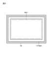
- FIG. 1 is a plan view of a display device according to a first embodiment.
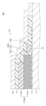
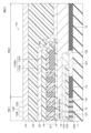
- FIG. 2 is a cross-sectional view taken along line II-II of FIG.
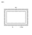
- FIG. 3 is a plan view of the light-shielding layer and the peripheral layer.
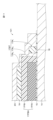
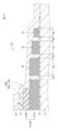
- FIG. 4 is an enlarged cross-sectional view showing the peripheral end portion of the light-shielding layer and its vicinity.
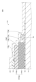
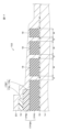
- FIG. 5 is a cross-sectional view of the display device according to the second embodiment.
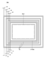
- FIG. 6 is a plan view of a light-shielding layer and multiple peripheral layers.
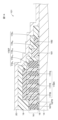
- FIG. 7 is a cross-sectional view of a display device according to a modified example.
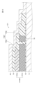
- FIG. 8 is a cross-sectional view of a display device according to a modified example.
- FIG. 1 is a plan view of a display device according to a first embodiment.
- FIG. 2 is a cross-sectional view taken along line II-II of FIG.
- FIG. 3 is a plan view of the
- FIG. 9 is a cross-sectional view of a display device according to a modified example.
- FIG. 10 is a cross-sectional view of a display device according to a modified example.
- FIG. 11 is a cross-sectional view of a display device according to a modified example.
- FIG. 12 is a cross-sectional view of a display device according to a modified example.
- FIG. 13 is a plan view of a light-shielding layer and multiple peripheral layers.
- FIG. 14 is a cross-sectional view of a display device according to a modified example.
- FIG. 15 is a cross-sectional view of a display device according to a modified example.
- FIG. 16 is a cross-sectional view of a display device according to a modified example.
- FIG. 17 is a cross-sectional view of a display device according to a modified example.
- FIG. 18 is a plan view of a light-shielding layer and multiple peripheral layers.
- FIG. 19 is a cross-sectional view of a display device according to a modified example.
- FIG. 20 is a plan view of the light-shielding layer and the peripheral layer.
- FIG. 21 is a plan view of a light-shielding layer and multiple peripheral layers.
- FIG. 22 is a plan view of a light-shielding layer and multiple peripheral layers.
- FIG. 23 is a cross-sectional view of a display device according to a modified example.
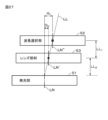
- 24A, 24B, and 24C are conceptual diagrams for explaining the relationship between a normal line LN passing through the center of the light-emitting portion, a normal line LN' passing through the center of the lens member, and a normal line LN" passing through the center of the wavelength selection portion, respectively.
- FIG. 25 is a conceptual diagram for explaining the relationship between a normal line LN passing through the center of the light emitting portion, a normal line LN' passing through the center of the lens member, and a normal line LN" passing through the center of the wavelength selecting portion.
- FIG. 26A and 26B are conceptual diagrams for explaining the relationship between a normal line LN passing through the center of the light-emitting portion, a normal line LN' passing through the center of the lens member, and a normal line LN" passing through the center of the wavelength selection portion, respectively.
- FIG. 27 is a conceptual diagram for explaining the relationship between a normal line LN passing through the center of the light emitting portion, a normal line LN' passing through the center of the lens member, and a normal line LN" passing through the center of the wavelength selecting portion.
- Fig. 28A is a schematic cross-sectional view for explaining a first example of a resonator structure
- Fig. 28B is a schematic cross-sectional view for explaining a second example of a resonator structure.
- FIG. 29A and 29B are schematic cross-sectional views for explaining a third example of the resonator structure and a fourth example of the resonator structure, respectively.
- 30A and 30B are schematic cross-sectional views for explaining a fifth example of the resonator structure and a sixth example of the resonator structure, respectively.
- FIG. 31 is a schematic cross-sectional view for explaining a seventh example of the resonator structure.
- 32A and 32B are front and rear views of the digital still camera.
- FIG. 33 is a perspective view of a head mounted display.
- FIG. 34 is a perspective view of a television device.
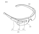
- FIG. 35 is a perspective view of a see-through head mounted display.
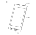
- FIG. 36 is a perspective view of a smartphone.
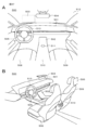
- Fig. 37A is a diagram showing the interior of the vehicle from the rear to the front
- Fig. 37B is a diagram showing the interior of the vehicle from the diagonally rear to the diagonally front.
- the display device of the present disclosure comprises a light-shielding layer surrounding a display area, a first peripheral layer surrounding the light-shielding layer, and a protective layer covering the light-shielding layer and the first peripheral layer, wherein the light-shielding layer includes a first colored layer and a second colored layer provided on the first colored layer, and the height of the upper surface of the first peripheral layer is lower than the height of the upper surface of the first colored layer.
- a height difference can be formed between the upper surface of the first peripheral layer and the upper surface of the light-shielding layer, so that the protective layer can be gradually lowered near the outer end of the light-shielding layer. Therefore, deterioration of the throwing power of the protective layer at the outer end of the light-shielding layer can be suppressed.
- the first peripheral layer is preferably made of the same material as the second colored layer. This allows the first peripheral layer to be formed in the same process as the second colored layer.
- the first peripheral layer is preferably made of the same material as the second colored layer and has approximately the same thickness as the second colored layer, and more preferably the thickness of the second colored layer is thinner than the thickness of the first colored layer. This allows the first peripheral layer to be more easily formed in the same process as the second colored layer.
- “approximately the same thickness” includes the same thickness.
- the outer end of the second colored layer is preferably recessed further inward than the outer end of the first colored layer. This allows a height difference (step) to be formed between the upper surface of the first colored layer and the upper surface of the second colored layer, preventing the outer end of the light-shielding layer from becoming too steep.
- the light-shielding layer preferably includes a third colored layer disposed on the second colored layer, and the outer end of the third colored layer is recessed further inward than the outer end of the second colored layer. This allows a height difference (step) to be formed between the upper surface of the second colored layer and the upper surface of the third colored layer, thereby preventing the outer end of the light-shielding layer from becoming too steep.
- the display device further includes a second peripheral layer surrounding the first peripheral layer, the first peripheral layer being made of the same material as the second colored layer, and the second peripheral layer being made of the same material as the third colored layer. This allows the first peripheral layer to be formed in the same process as the second colored layer, and the second peripheral layer to be formed in the same process as the third colored layer.
- the display device further includes a second peripheral layer surrounding the first peripheral layer, the first peripheral layer being made of the same material as the second colored layer, and having approximately the same thickness as the second colored layer, and the second peripheral layer being made of the same material as the third colored layer, and having approximately the same thickness as the third colored layer, and it is more preferable that the thickness of the second colored layer is thinner than the thickness of the first colored layer, and the thickness of the third colored layer is thinner than the thickness of the second colored layer. This allows the first peripheral layer to be more easily formed in the same process as the second colored layer, and the second peripheral layer to be more easily formed in the same process as the third colored layer.
- the display device further includes a second peripheral layer surrounding the first peripheral layer, and it is preferable that the height of the upper surface of the second peripheral layer is lower than the height of the upper surface of the first peripheral layer. This allows the protective layer to be gradually lowered near the outer end of the light-shielding layer.
- the display device further includes a second peripheral layer surrounding the first peripheral layer, and the second peripheral layer is preferably divided in the circumferential direction of the display area. This allows the material for forming the protective layer to penetrate into the divided portion of the second peripheral layer during the protective layer formation process, so that the protective layer can be gradually lowered near the outer end of the light-shielding layer.
- the display device further includes a second peripheral layer surrounding the first peripheral layer, and the first and second peripheral layers are preferably divided in the circumferential direction of the display area, with the number of division points in the second peripheral layer being greater than the number of division points in the first peripheral layer.
- the display device further includes a third peripheral layer, the third peripheral layer being provided on a terrace portion formed by recessing the outer end of the second colored layer inward from the outer end of the first colored layer, and it is preferable that the third peripheral layer recesses inward from the outer end of the first colored layer, and the height of the upper surface of the third peripheral layer is lower than the height of the upper surface of the second colored layer.
- This makes it possible to form a height difference (step) between the upper surface of the third peripheral layer and the upper surface of the second colored layer, and also to form a height difference (step) between the upper surface of the third peripheral layer and the upper surface of the first colored layer. Therefore, it is possible to prevent the outer end of the light-shielding layer from becoming steep.
- the display device further comprises a planarization layer provided between the light-shielding layer and the protective layer, and the third peripheral layer is preferably made of the same material as the planarization layer. This allows the third peripheral layer to be formed in the same process as the planarization layer.
- the display device further comprises a planarization layer provided between the light-shielding layer and the protective layer, and the third peripheral layer is preferably made of the same material as the planarization layer and has approximately the same thickness as the planarization layer, and more preferably the thickness of the planarization layer is thinner than the thickness of the second colored layer. This allows the third peripheral layer to be more easily formed in the same process as the planarization layer.
- the display device further includes a planarization layer provided between the light-shielding layer and the protective layer, and the end of the planarization layer is preferably recessed inward from the outer end of the second colored layer. This allows a height difference (step) to be formed between the upper surface of the second colored layer and the upper surface of the planarization layer, thereby preventing the light-shielding layer and the planarization layer from forming a steep end.
- the first peripheral layer is preferably made of the same material as the planarization layer. This allows the first peripheral layer to be formed in the same process as the planarization layer.
- the first peripheral layer is preferably made of the same material as the planarization layer and has approximately the same thickness as the planarization layer, and more preferably the thickness of the planarization layer is thinner than the thickness of the first colored layer. This allows the first peripheral layer to be more easily formed in the same process as the planarization layer.
- the display device further includes a second peripheral layer surrounding the first peripheral layer, the first peripheral layer being made of the same material as the second colored layer, and the second peripheral layer being made of the same material as the planarization layer. This allows the first peripheral layer to be formed in the same process as the second colored layer, and the second peripheral layer to be formed in the same process as the planarization layer.
- the display device further includes a second peripheral layer surrounding the first peripheral layer, the first peripheral layer being made of the same material as the second colored layer, and having approximately the same thickness as the second colored layer, and the second peripheral layer being made of the same material as the planarization layer, and having approximately the same thickness as the planarization layer, and more preferably the thickness of the second colored layer is thinner than the thickness of the first colored layer, and the thickness of the planarization layer is thinner than the thickness of the second colored layer.
- the display device further includes a planarization layer provided between the light-shielding layer and the protective layer, the planarization layer covering the outer edge of the light-shielding layer and the first peripheral layer, and the planarization layer preferably contains a positive-type photosensitive resin composition.
- a positive-type photosensitive resin composition is more likely to form a forward taper than a negative-type photosensitive resin composition, and therefore it is easier to make the edge of the planarization layer more gentle.
- the first peripheral layer and the light-shielding layer form a step shape with three or more steps that descend with increasing distance from the display area.
- the protective layer is formed to conform to the step shape, so that the protective layer can be gradually lowered at the outer end of the light-shielding layer and in its vicinity.
- the number of steps is counted based on the surface on which the first peripheral layer is formed.
- the display device includes a light-shielding layer surrounding a display area, multiple peripheral layers having a concentric shape surrounding the light-shielding layer, and a protective layer covering the light-shielding layer and the multiple peripheral layers, and the spacing between the multiple peripheral layers becomes wider as they move away from the display area to the outside, or the width of the multiple peripheral layers becomes narrower as they move away from the display area to the outside.
- the protective layer can be gradually lowered near the outer edge of the light-shielding layer. This makes it possible to suppress deterioration of the throwing power of the protective layer at the edge of the light-shielding layer.
- the width of the multiple peripheral layers narrows as they move outward from the display area, the amount of material forming the protective layer placed on the upper surface of the peripheral layers decreases as they move outward from the display area during the protective layer formation process. Therefore, the protective layer can be gradually lowered near the outer edge of the light-shielding layer. This makes it possible to suppress deterioration of the throwing power of the protective layer at the edge of the light-shielding layer.
- the light-shielding layer includes a first colored layer and a second colored layer provided on the first colored layer, and it is preferable that the multiple peripheral layers are made of the same material as the first colored layer. This allows the first colored layer and the multiple peripheral layers to be formed in the same process.
- the height of the multiple peripheral layers decreases with increasing distance from the display area to the outside. This allows a height difference (step) to be formed between adjacent peripheral layers, making it easier to gradually lower the protective layer near the outer edge of the light-shielding layer.
- the display device includes a light-shielding layer surrounding a display area, a plurality of peripheral layers having a concentric shape surrounding the light-shielding layer, and a protective layer covering the light-shielding layer and the plurality of peripheral layers, the plurality of peripheral layers including a plurality of divided peripheral layers that are divided in the circumferential direction of the display area, and the number of divided points in the plurality of divided peripheral layers increases the farther the divided peripheral layers are from the display area.
- the multiple peripheral layers include multiple divided peripheral layers that are divided in the circumferential direction of the display area, and the number of divided points in the multiple divided peripheral layers increases the farther the divided peripheral layers are from the display area.
- the protective layer formation process the amount of protective layer formation material that penetrates into the divided points of the peripheral layers increases as the distance from the display area increases. Therefore, the protective layer can be gradually lowered near the outer end of the light-shielding layer. This makes it possible to suppress deterioration of the throwing power of the protective layer at the end of the light-shielding layer.
- the light-shielding layer may include two colored layers or three colored layers.
- the two colored layers may include a first colored layer and a second colored layer provided on the first colored layer. It is preferable that the first colored layer and the second colored layer have different colors.
- the color combination of the first colored layer and the second colored layer is preferably red and blue. By selecting this color combination, the light-shielding ability of the light-shielding layer against visible light can be improved.
- the light-shielding layer can be formed in the same process as the color filter of the display area.
- the three colored layers may include a first colored layer, a second colored layer provided on the first colored layer, and a third colored layer provided on the second colored layer. It is preferable that the first colored layer, the second colored layer, and the third colored layer have different colors. By selecting this color combination, the light-blocking properties of the light-blocking layer against visible light can be improved. In addition, the light-blocking layer can be formed in the same process as the color filters in the display area.
- top surface refers to the surface on the display surface side of the display device.
- top surface height refers to the height based on the surface on which the light-shielding layer is provided. For example, when the light-shielding layer is provided on the top surface of the planarizing layer or the top surface of the protective layer, “top surface height” refers to the height based on the top surface of the planarizing layer or the top surface of the protective layer.
- the "outer end” refers to an end located on the outer side as viewed from the display area.
- the “inner side” refers to an end located on the inner side as viewed from the display area.
- the light-shielding layer (or the first colored layer) and the first peripheral layer may be separated or in contact with each other.
- the first peripheral layer and the second peripheral layer may be separated or in contact with each other.
- the third peripheral layer and the second colored layer may be separated or in contact with each other.
- the display device according to the present disclosure may be provided in an electronic device.
- the display device according to the present disclosure may be provided in an eyewear device such as a VR (Virtual Reality) device, an MR (Mixed Reality) device, or an AR (Augmented Reality) device, or may be provided in an electronic viewfinder (EVF) or a small projector, etc.
- an eyewear device such as a VR (Virtual Reality) device, an MR (Mixed Reality) device, or an AR (Augmented Reality) device
- EMF electronic viewfinder
- Fig. 1 is a plan view of a display device 101 according to a first embodiment.
- Fig. 2 is a cross-sectional view taken along line II-II in Fig. 1.
- the display device 101 may be a top-emission OLED display device.
- the display device 101 may be a microdisplay. As shown in Fig. 1, the display device 101 has a display region RE1 and a peripheral region RE2 provided around the display region RE1.
- Multiple sub-pixels 10R, 10G, 10B are two-dimensionally arranged in a specified arrangement pattern within the display region RE1.
- the specified arrangement pattern may be a stripe arrangement, a mosaic arrangement, a square arrangement, a delta arrangement, or any other arrangement.
- a pad section 101A and a driver (not shown) for displaying images are provided in the peripheral region RE2.
- a flexible printed circuit (Flexible Printed Circuit: FPC) (not shown) may be connected to the pad section 101A.
- Sub-pixel 10R can emit red light (first light).
- Sub-pixel 10G can emit green light (second light).
- Sub-pixel 10B can emit blue light (third light).
- sub-pixel 10R, 10G, and 10B when sub-pixels 10R, 10G, and 10B are referred to collectively without any particular distinction, they may be referred to as sub-pixel 10.
- One pixel is composed of, for example, multiple adjacent sub-pixels 10R, 10G, and 10B.
- the composition of one pixel is not limited to this example, and for example, one pixel may be composed of multiple adjacent sub-pixels 10R, 10G, 10B, and 10B.
- the display device 101 includes a drive substrate 11, a plurality of light-emitting elements 12W, a contact electrode 124, an insulating layer 13, a protective layer 14, a planarization layer 15, a color filter 16, a light-shielding layer 17FBK, a peripheral layer 18, a planarization layer 19, and a protective layer 20.
- the planarization layer 15 and the planarization layer 19 are provided as necessary, and may or may not be provided.
- the surface on the display surface side (top side) of the display device 101 may be referred to as the first surface (upper surface), and the surface on the opposite side (bottom side) of the display surface of the display device 101 may be referred to as the second surface (lower surface).
- the periphery or outer periphery of the first surface refers to an area having a predetermined width from the periphery of the first surface toward the inside
- the periphery or outer periphery of the second surface refers to an area having a predetermined width from the periphery of the second surface toward the inside.
- a planar view means a planar view when an object is viewed from a direction perpendicular to the first surface or the second surface.
- a being located outside B means that A is located outside B as viewed from the display area RE1
- a being located inside B means that A is located inside B as viewed from the display area RE1.
- when A is set back more inward than B this means that A is set back more inward than B when viewed from the display area RE1.
- the driving substrate 11 is a so-called backplane, and is capable of driving a plurality of light emitting elements 12 W.
- the driving substrate 11 includes, for example, a substrate and an insulating layer in this order.
- a plurality of driving circuits (not shown) and a plurality of wirings (not shown) may be provided on the first surface of the substrate.
- the substrate may be, for example, a semiconductor substrate on which transistors and the like can be easily formed, or a glass substrate or resin substrate with low moisture and oxygen permeability.
- the semiconductor substrate includes, for example, amorphous silicon, polycrystalline silicon, or single crystal silicon.
- the glass substrate includes, for example, high strain point glass, soda glass, borosilicate glass, forsterite, lead glass, or quartz glass.
- the resin substrate includes, for example, at least one selected from the group consisting of polymethyl methacrylate, polyvinyl alcohol, polyvinyl phenol, polyether sulfone, polyimide, polycarbonate, polyethylene terephthalate, and polyethylene naphthalate.
- the insulating layer may be provided on the first surface of the substrate, covering and planarizing the multiple drive circuits and multiple wirings, etc.
- the insulating layer may provide insulation between the multiple drive circuits and multiple wirings, etc. provided on the first surface of the substrate, and the multiple light-emitting elements 12W.
- the multiple wirings may be connected to the pad portion 101A.
- the insulating layer may be an organic insulating layer, an inorganic insulating layer, or a laminate thereof.
- the organic insulating layer includes at least one selected from the group consisting of, for example, polyimide resin, acrylic resin, and novolac resin.
- the inorganic insulating layer includes at least one selected from the group consisting of, for example, silicon oxide (SiO x ), silicon nitride (SiN x ), and silicon oxynitride (SiO x N y ).
- the insulating layer has multiple contact parts (not shown) therein.
- the multiple contact parts provided in the display region RE1 electrically connect the light-emitting elements to the wiring.
- the multiple contact parts provided in the peripheral region RE2 electrically connect the contact electrodes 124 to the wiring.
- the contact parts include at least one metal selected from the group consisting of, for example, copper (Cu) and titanium (Ti).
- the light-emitting element 12W can emit white light based on the control of a drive circuit, etc.
- the light-emitting element 12W may be an OLED element.
- the OLED element may be a Micro-OLED (M-OLED) element.
- the light-emitting element 12W is included in the sub-pixels 10R, 10G, and 10B of each color.
- the multiple light-emitting elements 12W are two-dimensionally arranged in a specified arrangement pattern on the first surface of the drive substrate 11.
- the specified arrangement pattern is as described above as the specified arrangement pattern of the multiple sub-pixels 10.
- the light-emitting element 12W includes a first electrode 121, an OLED layer 122, and a second electrode 123, which are arranged in that order on the first surface of the drive substrate 11.
- the first electrode 121 is provided on the second surface side of the OLED layer 122.
- the first electrode 121 is an individual electrode provided for each of the light emitting elements 12W in the display region RE1. That is, the first electrode 121 is divided between the light emitting elements 12W adjacent to each other in the in-plane direction of the first surface of the drive substrate 11 in the display region RE1.
- the first electrode 121 is an anode. When a voltage is applied between the first electrode 121 and the second electrode 123, holes are injected from the first electrode 121 to the OLED layer 122.
- the first electrode 121 may be composed of, for example, a metal layer, or may be composed of a metal layer and a transparent conductive oxide layer.
- the transparent conductive oxide layer is provided on the OLED layer 122 side, from the viewpoint of having a layer having a high work function adjacent to the OLED layer 122.
- the metal layer may function as a reflective layer that reflects light emitted by the OLED layer 122.
- the metal layer contains at least one metal element selected from the group consisting of chromium (Cr), gold (Au), platinum (Pt), nickel (Ni), copper (Cu), molybdenum (Mo), titanium (Ti), tantalum (Ta), aluminum (Al), magnesium (Mg), iron (Fe), tungsten (W) and silver (Ag).
- the metal layer may contain at least one metal element as an alloy component. Specific examples of the alloy include an aluminum alloy or a silver alloy. Specific examples of the aluminum alloy include AlNd or AlCu.
- a base layer may be provided adjacent to the second surface side of the metal layer.
- the base layer may be capable of improving the crystal orientation of the metal layer when the metal layer is formed.
- the base layer may contain at least one metal element selected from the group consisting of titanium (Ti) and tantalum (Ta), for example.
- the base layer may contain the at least one metal element as a constituent element of an alloy.
- the transparent conductive oxide layer includes a transparent conductive oxide.
- the transparent conductive oxide includes at least one type selected from the group consisting of transparent conductive oxides containing indium (hereinafter referred to as "indium-based transparent conductive oxides"), transparent conductive oxides containing tin (hereinafter referred to as “tin-based transparent conductive oxides”), and transparent conductive oxides containing zinc (hereinafter referred to as “zinc-based transparent conductive oxides").
- Indium-based transparent conductive oxides include, for example, indium tin oxide (ITO), indium zinc oxide (IZO), indium gallium oxide (IGO), indium gallium zinc oxide (IGZO) or fluorine-doped indium oxide (IFO).
- ITO indium tin oxide
- ITO indium tin oxide
- Tin-based transparent conductive oxides include, for example, tin oxide, antimony-doped tin oxide (ATO) or fluorine-doped tin oxide (FTO).
- Zinc-based transparent conductive oxides include, for example, zinc oxide, aluminum-doped zinc oxide (AZO), boron-doped zinc oxide or gallium-doped zinc oxide (GZO).
- the OLED layer 122 can emit white light.
- the OLED layer 122 is provided between a plurality of first electrodes 121 and one second electrode 123.
- the OLED layer 122 is , which is connected between adjacent light emitting elements 12W in the in-plane direction of the first surface of the drive substrate 11, is a layer common to a plurality of light emitting elements 12W in the display region RE1.
- the OLED layer 122 may be composed of a laminate including an organic light-emitting layer, and in that case, some layers of the laminate (e.g., an electron injection layer) may be inorganic layers.
- the OLED layer 122 may be an OLED layer having a single light-emitting unit, an OLED layer having two light-emitting units (tandem structure), or an OLED layer having a structure other than these.
- An OLED layer having a single light-emitting unit has a structure in which, for example, a hole injection layer, a hole transport layer, a red light-emitting layer, a light-emitting separation layer, a blue light-emitting layer, a green light-emitting layer, an electron transport layer, and an electron injection layer are stacked in this order from the first electrode 121 to the second electrode 123.
- An OLED layer having two light-emitting units has a structure in which, for example, a hole injection layer, a hole transport layer, a blue light-emitting layer, an electron transport layer, a charge generation layer, a hole transport layer, a yellow light-emitting layer, an electron transport layer, and an electron injection layer are stacked in this order from the first electrode 121 to the second electrode 123.
- the hole injection layer can increase the efficiency of hole injection into each light-emitting layer and suppress leakage.
- the hole transport layer can increase the efficiency of hole transport into each light-emitting layer.
- the electron injection layer can increase the efficiency of electron injection into each light-emitting layer.
- the electron transport layer can increase the efficiency of electron transport into each light-emitting layer.
- the light-emitting separation layer is a layer for adjusting the injection of carriers into each light-emitting layer, and the light emission balance of each color is adjusted by injecting electrons and holes into each light-emitting layer through the light-emitting separation layer.
- the charge generation layer can supply electrons and holes to the two light-emitting layers arranged to sandwich the charge generation layer.
- red, green, blue, and yellow light-emitting layers When an electric field is applied to the red, green, blue, and yellow light-emitting layers, recombination occurs between holes injected from the first electrode 121 or the charge generation layer and electrons injected from the second electrode 123 or the charge generation layer, and the red, green, blue, and yellow light-emitting layers can emit light, green, blue, and yellow, respectively.
- the second electrode 123 is provided on the first surface side of the OLED layer 122.
- the second electrode 123 is connected between adjacent light emitting elements 12W in the in-plane direction of the first surface of the drive substrate 11 in the display region RE1, and is a common electrode for the plurality of light emitting elements 12W in the display region RE1.
- the second electrode 123 extends from the display region RE1 to the peripheral region RE2.
- the peripheral portion of the second surface of the second electrode 123 is connected to the first surface of the contact electrode 124.
- the second electrode 123 is a cathode. When a voltage is applied between the first electrode 121 and the second electrode 123, electrons are injected from the second electrode 123 into the OLED layer 122.
- the second electrode 123 is translucent to the white light emitted from the OLED layer 122.
- the second electrode 123 is preferably a transparent electrode that is transparent to visible light. In this specification, visible light refers to light in the wavelength range of 360 nm or more and 830 nm.
- the second electrode 123 is preferably made of a material with as high a light transmittance as possible and a small work function in order to increase the light emission efficiency.
- the second electrode 123 is made of, for example, at least one layer of a metal layer and a transparent conductive oxide layer. More specifically, the second electrode 123 is made of a single layer film of a metal layer or a transparent conductive oxide layer, or a laminated film of a metal layer and a transparent conductive oxide layer.
- the metal layer may be provided on the OLED layer 122 side, or the transparent conductive oxide layer may be provided on the OLED layer 122 side. However, from the viewpoint of having a layer with a low work function adjacent to the OLED layer 122, it is preferable that the metal layer is provided on the OLED layer 122 side.
- the metal layer contains at least one metal element selected from the group consisting of magnesium (Mg), aluminum (Al), silver (Ag), calcium (Ca) and sodium (Na).
- the metal layer may contain at least one of the metal elements as a constituent element of an alloy. Specific examples of the alloy include an MgAg alloy, an MgAl alloy, and an AlLi alloy.
- the transparent conductive oxide layer contains a transparent conductive oxide. Examples of the transparent conductive oxide include materials similar to the transparent conductive oxide of the first electrode 121 described above.
- the contact electrode 124 is provided on the first surface of the drive substrate 11 in the peripheral region RE2.
- the contact electrode 124 is an auxiliary electrode that connects the second electrode 123 to wiring (not shown) in the drive substrate 11.
- the first surface of the contact electrode 124 is electrically connected to the periphery of the second surface of the second electrode 123.
- the second surface of the contact electrode 124 is connected to the wiring via a plurality of contact portions or the like.
- the contact electrode 124 may have a closed loop shape that surrounds the entire outer periphery of the display region RE1, or may have a loop shape that surrounds the outer periphery of the display region RE1 and is interrupted at one or more points.
- the contact electrode 124 is composed of, for example, at least one layer of a metal layer and a metal oxide layer. More specifically, for example, the contact electrode 124 is composed of a single layer film of a metal layer or a metal oxide layer, or a laminate film of a metal layer and a metal oxide layer. It is preferable that the contact electrode 124 has a similar configuration to the first electrode 121 described above. In this case, the first electrode 121 and the contact electrode 124 can be formed in the same process, so that the manufacturing process of the display device 101 can be simplified.
- Examples of the material contained in the contact electrode 124 include the same material as the first electrode 121 described above. Specifically, examples of the material contained in the metal layer of the contact electrode 124 include the same material as the metal layer of the first electrode 121 described above, and examples of the material contained in the metal oxide layer of the contact electrode 124 include the same material as the metal oxide layer of the first electrode 121 described above.
- a base layer (not shown) may be provided adjacent to the second surface side of the metal layer.
- Examples of materials contained in the base layer include the same materials as those of the base layer of the first electrode 121 described above.
- the insulating layer 13 is provided in a portion between the separated first electrodes 121 on the first surface of the driving substrate 11.
- the insulating layer 13 can insulate between the first electrodes 121 adjacent in the in-plane direction of the first surface of the driving substrate 11.
- the insulating layer 13 has a plurality of first openings 131.
- the plurality of first openings 131 are provided corresponding to each light-emitting element 12W.
- the plurality of first openings 131 may be provided on the first surface (the surface on the OLED layer 122 side) of each first electrode 121.
- the first electrode 121 and the OLED layer 122 are in contact with each other through the first openings 131.
- the insulating layer 13 is also provided between the first electrode 121 and the contact electrode 124 on the first surface of the drive substrate 11.
- the insulating layer 13 can insulate between the first electrode 121 and the contact electrode 124.
- the insulating layer 13 has a second opening 132.
- the second opening 132 is provided corresponding to the contact electrode 124.
- the second opening 132 may be provided on the first surface of the contact electrode 124 (the surface connected to the peripheral portion of the second electrode 123).
- the contact electrode 124 and the peripheral portion of the second electrode 123 come into contact with each other through the second opening 132.
- the second opening 132 may have a loop shape similar to that of the contact electrode 124.
- the insulating layer 13 may be an organic insulating layer, an inorganic insulating layer, or a laminate thereof.
- the organic insulating layer includes at least one selected from the group consisting of polyimide resin, acrylic resin, novolac resin, etc.
- the inorganic insulating layer includes at least one selected from the group consisting of silicon oxide (SiO x ), silicon nitride (SiN x ), silicon oxynitride (SiO x N y ), etc.
- the protective layer 14 is provided on the first surface of the second electrode 123 and covers the plurality of light-emitting elements 12W.
- the protective layer 14 is translucent to the white light emitted from the light-emitting elements 12W.
- the protective layer 14 is preferably transparent to visible light.
- the protective layer 14 can protect the plurality of light-emitting elements 12W and the like.
- the protective layer 14 can suppress the intrusion of moisture from the external environment into the plurality of light-emitting elements 12W.
- the protective layer 14 may have a function of suppressing oxidation of the metal layer.
- the protective layer 14 includes, for example, an inorganic material or an organic material with low hygroscopicity.
- the protective layer 14 may have a single-layer structure or a multi-layer structure. When the thickness of the protective layer 14 is increased, it is preferable to use a multi-layer structure. This is to relieve internal stress in the protective layer 14.
- the inorganic material includes, for example, at least one selected from the group consisting of silicon oxide (SiO x ), silicon nitride (SiN x ), silicon oxynitride (SiO x N y ), titanium oxide (TiO x ), and aluminum oxide (AlO x ).
- the organic material includes, for example, at least one cured resin selected from the group consisting of thermosetting resin and ultraviolet curing resin.
- the organic material includes, for example, at least one selected from the group consisting of acrylic resin, polyimide resin, novolac resin, epoxy resin, norbornene resin, and parylene resin.
- the protective layer 14 preferably includes a deposition layer in which a monolayer is deposited.
- the deposition layer may be an ALD (Atomic Layer Deposition) layer.
- ALD Advanced Layer Deposition
- the deposition layer includes, for example, a metal oxide or a metal nitride.
- the metal oxide includes, for example, aluminum oxide (AlO x ) or titanium oxide (TiO x ).
- the metal nitride includes, for example, titanium nitride (TiN x ).
- the planarization layer 15 is provided on the first surface of the protective layer 14.
- the planarization layer 15 can fill the unevenness of the first surface of the protective layer 14 to form a flat first surface above the protective layer 14.
- the planarization layer 15 is translucent to the white light emitted from the light-emitting element 12W.
- the planarization layer 15 is preferably transparent to visible light.
- the planarization layer 15 includes, for example, an inorganic material or an organic material. Examples of the inorganic material include the same material as the inorganic material of the protective layer 14. Examples of the organic material include the same material as the organic material of the protective layer 14.
- the organic material may include a cured product of a photosensitive resin composition.
- the photosensitive resin composition may include either a positive-type photosensitive resin composition or a negative-type photosensitive resin composition.
- Specific examples of photosensitive resin compositions include at least one selected from the group consisting of polyimide, polyimide precursor, polybenzoxazole, polybenzoxazole precursor, acrylic resin, phenolic resin, and siloxane resin, but are not limited to these materials.
- the color filter 16 is provided above the plurality of light-emitting elements 12W. More specifically, the color filter 16 is provided on a first surface of the planarization layer 15 in the display region RE1.
- the color filter 16 is, for example, an on-chip color filter (OCCF).
- the color filter 16 includes, for example, a plurality of colored layers 16FR, a plurality of colored layers 16FG, and a plurality of colored layers 16FB. In the following description, when the colored layers 16FR, 16FG, and 16FB are collectively referred to without any particular distinction, they may be referred to as the colored layer 16F.
- the multiple colored layers 16F are two-dimensionally arranged on the first surface of the planarization layer 15 in a specified arrangement pattern.
- the specified arrangement pattern is as described above as the specified arrangement pattern of the multiple sub-pixels 10.
- Each colored layer 16F is provided above the light-emitting element 12W.
- the sub-pixel 10R is composed of the light-emitting element 12W and a colored layer 16FR provided above the light-emitting element 12W.
- the sub-pixel 10G is composed of the light-emitting element 12W and a colored layer 16FG provided above the light-emitting element 12W.
- the sub-pixel 10B is composed of the light-emitting element 12W and a colored layer 16FB provided above the light-emitting element 12W.
- the coloring layer 16FR has a red color.
- the coloring layer 16FR transmits the red light component of the white light emitted from the light-emitting element 12W, but can absorb visible light components other than red light.
- the coloring layer 16FG has a green color.
- the coloring layer 16FG transmits the green light component of the white light emitted from the light-emitting element 12W, but can absorb visible light components other than green light.
- the coloring layer 16FB has a blue color.
- the coloring layer 16FB transmits the blue light component of the white light emitted from the light-emitting element 12W, but can absorb visible light components other than blue light.
- the thickness of the coloring layer 16FR may be thinner than the thickness of the coloring layer 16FG.
- the thickness of the coloring layer 16FB may be thinner than the thickness of the coloring layer 16FR.
- Colored layer 16FR includes, for example, a red color resist.
- Colored layer 16FG includes, for example, a green color resist.
- Colored layer 16FB includes, for example, a blue color resist.
- Light blocking layer 17FBK 3 is a plan view of the light-shielding layer and the peripheral layer.
- FIG. 4 is an enlarged cross-sectional view of the peripheral end of the light-shielding layer 17FBK and its vicinity.
- the light-shielding layer 17FBK is a planarized layer in the peripheral region RE2.
- the light-shielding layer 17FBK is provided on the first surface of the layer 15.
- the light-shielding layer 17FBK is located above the contact electrode 124, and preferably covers the upper part of the contact electrode 124.
- the light-shielding layer 17FBK is configured to block incident light into the peripheral region RE2. This makes it possible to suppress reflection of the external light at the contact electrodes 124 and the like. It may have a closed loop shape surrounding the entire outer periphery, or it may have a loop shape surrounding the outer periphery of the display area RE1 and being divided at one or more points. Example shapes are shown.
- the light-shielding layer 17FBK includes a colored layer 17FR and a colored layer 17FB.
- the colored layer 17FR may be provided on the first surface of the flattening layer 15, and the colored layer 17FB may be provided on the first surface of the colored layer 17FR.
- the order of lamination of the colored layer 17FB and the colored layer 17FR is not particularly limited, and the colored layer 17FB may be provided on the first surface of the flattening layer 15, and the colored layer 17FR may be provided on the first surface of the colored layer 17FB.
- the peripheral end of the colored layer 17FB on the outer periphery side is set back more inward than the peripheral end of the colored layer 17FR on the outer periphery side. As a result, a height difference 17A3 equal to the thickness of the colored layer 17FB is formed between the first surface of the colored layer 17FB and the first surface of the colored layer 17FR.
- the colored layer 17FR and the colored layer 17FG have different colors. It is preferable that the colored layer 17FR has a red color.
- the colored layer 17FR may have the same transmission characteristics and absorption characteristics as the colored layer 16FR.
- the colored layer 17FB has a blue color.
- the colored layer 17FB may have the same transmission characteristics and absorption characteristics as the colored layer 16FB.
- the colored layer 17FR is made of the same material as the colored layer 16FR and has approximately the same thickness as the colored layer 16FR.
- the colored layer 17FB is made of the same material as the colored layer 16FB and has approximately the same thickness as the colored layer 16FB.
- the color filter 16 and the light-shielding layer 17FBK can be formed in the same process.
- the thickness of colored layer 16FB may be thinner than the thickness of colored layer 16FR, and the thickness of colored layer 17FB may be thinner than the thickness of colored layer 17FR.
- the peripheral layer 18 is provided on the first surface of the planarization layer 15 in the peripheral region RE2.
- the peripheral layer 18 is located outside the peripheral end portion on the outer periphery side of the light shielding layer 17FBK and surrounds the peripheral end portion on the outer periphery side of the light shielding layer 17FBK.
- the peripheral layer 18 may have a closed loop shape surrounding the light shielding layer 17FBK in a plan view.
- the first surface of the peripheral layer may be a flat surface.
- the height of the first surface of the peripheral layer 18 is lower than the height of the first surface of the colored layer 17FR.
- a height difference 17A 2 smaller than the thickness of the colored layer 17FR is formed between the first surface of the peripheral layer 18 and the first surface of the colored layer 17FR.
- a height difference 17A 1 smaller than the thickness of the colored layer 17FR is formed between the first surface of the peripheral layer 18 and the first surface of the planarization layer 15.
- the width of the peripheral layer 18 is preferably 1 ⁇ m or more. When the width of the peripheral layer 18 is 1 ⁇ m or more, peeling of the peripheral layer 18 can be suppressed in the manufacturing process of the display device 101.
- the peripheral layer 18 is separated from the peripheral end portion on the outer periphery side of the light-shielding layer 17FBK, and a gap may be formed between the peripheral end portion on the inner periphery side of the peripheral layer 18 and the peripheral end portion on the outer periphery side of the light-shielding layer 17FBK.
- the width of the gap formed between the peripheral layer 18 and the light-shielding layer 17FBK (colored layer 17FR) is preferably 0.2 ⁇ m or more. When the width of the gap is 0.2 ⁇ m or more, overlapping of the peripheral layer 18 and the light-shielding layer 17FBK in the manufacturing process of the display device 101 can be suppressed.
- the peripheral layer 18 is made of the same material as the colored layer 17FB, and it is more preferable that the peripheral layer 18 is made of the same material as the colored layer 17FB and has approximately the same thickness as the colored layer 17FB.
- the peripheral layer 18 can be formed in the same process as the colored layer 17FB.
- the configuration of the peripheral layer 18 is not limited to the above example, and the peripheral layer 18 may be made of a different material than the colored layer 17FB, and the peripheral layer 18 may have a different thickness than the colored layer 17FB.
- the light-shielding layer 17FBK and the peripheral layer 18 form a stepped portion 17ST in the peripheral region RE2 on the first surface of the planarizing layer 15.
- the stepped portion 17ST has, for example, three steps consisting of height differences 17A1 , 17A2 , and 17A3 .
- planarization layer 19 The planarization layer 19 is provided on the first surface of the color filter 16 and covers the first surface of the color filter 16. It is preferable that the peripheral end of the planarization layer 19 is located outside the peripheral layer 18, and the planarization layer 19 further covers the stepped portion 17ST. The peripheral end of the planarization layer 19 may be located outside the peripheral end of the planarization layer 15, and the planarization layer 19 may further cover the peripheral end of the planarization layer 15.
- the planarization layer 19 is translucent to the light emitted from the color filter 16.
- the planarization layer 19 is preferably transparent to visible light.
- the planarization layer 19 can fill the irregularities on the first surface of the color filter 16 to form a flat first surface above the color filter 16.
- the planarization layer 15 may be capable of suppressing the intrusion of moisture from the external environment into the multiple light-emitting elements 12W.
- the thickness of the planarization layer 19 may be thinner than the thickness of the colored layer 17FB.
- the planarization layer 19 includes, for example, an inorganic material or an organic material. Examples of inorganic materials include materials similar to the inorganic material of the protective layer 14. Examples of organic materials include materials similar to the organic material of the protective layer 14.
- the organic material preferably contains a cured product of a photosensitive resin composition.
- the photosensitive resin composition may contain either a positive photosensitive resin composition or a negative photosensitive resin composition, but preferably contains a positive photosensitive resin composition.
- a positive photosensitive resin composition is easier to form a forward taper than a negative photosensitive resin composition, so that the peripheral edge of the planarization layer 19 is easier to make gentler.
- Specific examples of photosensitive resin compositions include materials similar to the photosensitive resin composition of the planarization layer 15, but are not limited to these materials.
- the protective layer 20 is provided on the first surface of the planarization layer 19, and covers the first surface of the planarization layer 19 and the step shape portion 17ST.
- the protective layer 20 may cover the entire first surface of the drive substrate 11.
- the protective layer 20 may have a step shape following the step shape portion 17ST.
- the protective layer 20 is translucent to the light emitted from the color filter 16.
- the protective layer 20 is preferably transparent to visible light.
- the protective layer 20 can protect the multiple light-emitting elements 12W and the like. For example, the protective layer 20 can suppress the intrusion of moisture from the external environment into the multiple light-emitting elements 12W.
- the protective layer 20 may be capable of improving the surface strength of the display surface.
- the protective layer 20 may be an inorganic layer formed by a vacuum film-forming technique such as CVD, or may be an organic layer (coating layer) formed by coating a resin composition.
- the protective layer 20 includes, for example, at least one of an inorganic material and an organic material.
- the organic material includes, for example, at least one of a thermosetting resin and an ultraviolet-curable resin.
- the protective layer 20 is preferably composed of a hard coat layer. This can improve the properties of the display device 101, such as scratch resistance and weather resistance.
- the hard coat layer includes, for example, an ultraviolet-curable resin.
- the ultraviolet-curable resin includes, for example, at least one selected from the group consisting of radical polymerization type ultraviolet-curable resins and cationic polymerization type ultraviolet-curable resins.
- the ultraviolet-curable resin may include additives as necessary.
- the additives include, for example, at least one selected from the group consisting of sensitizers, fillers, stabilizers, leveling agents, ultraviolet absorbers, antistatic agents, defoamers, and viscosity adjusters.
- the ultraviolet-curable resin may include, for example, an acrylic ultraviolet-curable resin.
- Step of forming the first electrode 121 and the contact electrode 124) First, a metal layer and a metal oxide layer are successively formed on the first surface of the drive substrate 11 by, for example, a sputtering method, and then the metal layer and the metal oxide layer are patterned by, for example, a photolithography technique. As a result, a plurality of first electrodes 121 and contact electrodes 124 are formed on the first surface of the drive substrate 11.
- the insulating layer 13 is formed on the first surface of the drive substrate 11 so as to cover the plurality of first electrodes 121 and the contact electrodes 124, for example, by a chemical vapor deposition (CVD) method.
- the plurality of first openings 131 and the second openings 132 are formed in the insulating layer 13, for example, by a photolithography technique.
- the plurality of first openings 131 and the second openings 132 are as described above.
- a hole transport layer, a red light-emitting layer, an emission separation layer, a blue light-emitting layer, a green light-emitting layer, an electron transport layer, and an electron injection layer are laminated in this order on the first surfaces of the plurality of first electrodes 121 and the first surface of the driving substrate 11, for example by a vapor deposition method, to form the OLED layer 122.
- Step of forming second electrode 123) the second electrode 123 is formed on the first surface of the OLED layer 122 and on the first surface of the contact electrode 124 by, for example, evaporation or sputtering. As a result, a plurality of light-emitting elements 12W are formed on the first surface of the drive substrate 11, and the peripheral portion of the second surface of the second electrode 123 is connected to the contact electrode 124.
- the protective layer 14 is formed on the first surface of the second electrode 123 by, for example, CVD or evaporation.
- Step of forming the planarizing layer 15 Next, for example, a photosensitive resin composition is applied onto the first surface of the protective layer 14, and then the photosensitive resin composition is exposed to light, developed, or the like, to form a planarizing layer 15 on the first surface of the protective layer 14.
- a green color resist is applied to the first surface of the planarization layer 15, and then the planarization layer 15 is pattern-exposed by irradiating ultraviolet light through a photomask, and then developed to form a plurality of colored layers 16FG.
- a red color resist is applied to the first surface of the planarization layer 15 so as to cover the plurality of colored layers 16FG, and then the planarization layer 15 is pattern-exposed by irradiating ultraviolet light through a photomask, and then developed to form a plurality of colored layers 16FR and one colored layer 17FR.
- a blue color resist is applied to the first surface of the planarization layer 15 so as to cover the plurality of colored layers 16FG, the plurality of colored layers 16FR, and one colored layer 17FR, and then the planarization layer 15 is pattern-exposed by irradiating ultraviolet light through a photomask, and then developed to form a plurality of colored layers 16FB, one colored layer 17FB, and one peripheral layer 18.
- one color filter 16, one light-shielding layer 17FBK, and one peripheral layer 18 are formed on the first surface of the planarization layer 15.
- Step of forming planarizing layer 19 Next, for example, a photosensitive resin composition is applied onto the first surfaces of the color filter 16, the light-shielding layer 17FBK, and the peripheral layer 18, and then the photosensitive resin composition is exposed to light, developed, etc., to form a planarization layer 19 that covers the color filter 16, the light-shielding layer 17FBK, and the peripheral layer 18.
- the protective layer 20 is formed on the first surface of the planarization layer 19 by a vacuum film formation technique such as a CVD method.
- a vacuum film formation technique such as a CVD method.
- the method of forming the protective layer 20 is not limited to this example, and the protective layer 20 may be formed, for example, by applying a curable resin onto the first surface of the planarization layer 19 and curing it.
- the peripheral layer 18 surrounds the peripheral end portion on the outer periphery side of the light-shielding layer 17FBK, and the height of the first surface of the peripheral layer 18 is lower than the height of the first surface of the colored layer 17FR.
- a height difference 17A2 smaller than the thickness of the colored layer 17FR is formed between the first surface of the colored layer 17FR and the first surface of the peripheral layer 18.
- a height difference 17A1 smaller than the thickness of the colored layer 17FR is formed between the first surface of the peripheral layer 18 and the first surface of the planarization layer 15.
- the peripheral edge of the colored layer 17FB on the outer periphery side is recessed further inward than the peripheral edge of the colored layer 17FR on the outer periphery side, thereby forming a height difference 17A3 between the first surface of the colored layer 17FB and the first surface of the colored layer 17FR. Therefore, a three-stepped portion 17ST consisting of height differences 17A 1 , 17A 2 and 17A 3 is formed by the light-shielding layer 17FBK and the peripheral layer 18.
- the step-shaped portion 17ST gradually descends as it moves away from the display region RE1. This makes it possible to suppress the deterioration of the throwing power of the protective layer 20 at the peripheral end of the light-shielding layer 16FBK.
- the protective layer 20 is formed by a vacuum film-forming technique such as CVD, it is possible to suppress the deterioration of the throwing power of the protective layer 20 at the peripheral end of the light-shielding layer 16FBK. Therefore, it is possible to suppress the deterioration of the function of the protective layer 20, and therefore the deterioration of the durability of the display device 101 can be suppressed.
- FIG. 5 is a cross-sectional view of a display device 102 according to a second embodiment.
- the display device 102 includes a plurality of peripheral layers 18.
- the plurality of peripheral layers 18 are located outside the outer peripheral end of the light-shielding layer 17FBK and have a concentric shape surrounding the display region RE1.
- the interval D between adjacent peripheral layers 18 becomes wider as they move away from the display region RE1.
- the plurality of peripheral layers 18 may have substantially the same thickness regardless of the distance from the display region RE1.
- the width W of the plurality of peripheral layers 18 may be the same regardless of the distance from the display region RE1.
- the interval d between the peripheral layer 18 closest to the display region RE1 and the colored layer 17FR may be narrower than the interval D between the peripheral layer 18 closest to the display region RE1 and the peripheral layer 18 second closest to the display region RE1, or may be substantially equal to the distance.
- the width W of the peripheral layer 18 is preferably set to 1 ⁇ m or more. When the width W of the peripheral layer 18 is 1 ⁇ m or more, peeling of the peripheral layer 18 can be suppressed during the manufacturing process of the display device 102.
- the distance D between adjacent peripheral layers 18 is preferably set to 0.2 ⁇ m or more. When the distance D between adjacent peripheral layers 18 is 0.2 ⁇ m or more, overlapping of adjacent peripheral layers 18 can be suppressed during the manufacturing process of the display device 102.
- the multiple peripheral layers 18 are preferably made of the same material as the colored layer 17FR or colored layer 17FB. This allows the colored layer 17FR or colored layer 17FB and the peripheral layer 18 to be formed in the same process.
- the peripheral edge of the flattening layer 19 may be recessed inward from the peripheral edge of the light-shielding layer 17FBK, specifically, the peripheral edge of the colored layer 17FB. In this case, a height difference 17A4 is formed between the first surface of the flattening layer 19 and the first surface of the light-shielding layer 17FBK.
- the protective layer 20 covers the planarization layer 19, the light-shielding layer 17FBK, and the multiple peripheral layers 18.
- the first surface of the protective layer 20 gradually descends as it moves away from the outer peripheral end of the light-shielding layer 17FBK.
- the descending first surface of the protective layer 20 may be an inclined surface, may be stepped, or may be a surface that combines both.
- a plurality of colored layers 16FG are formed in the same manner as the formation process of the colored layer 16FG in the first embodiment.
- a red color resist is applied to the first surface of the planarization layer 15 so as to cover the plurality of colored layers 16FG, and is then irradiated with ultraviolet light through a photomask to perform pattern exposure, followed by development to form a plurality of colored layers 16FR, one colored layer 17FR, and a plurality of peripheral layers 18.
- a blue color resist is applied to the first surface of the planarization layer 15 so as to cover the plurality of colored layers 16FG, the plurality of colored layers 16FR, one colored layer 17FR, and a plurality of peripheral layers 18, and is then irradiated with ultraviolet light through a photomask to perform pattern exposure, followed by development to form a plurality of colored layers 16FB and one colored layer 17FB.
- one color filter 16, one light-shielding layer 17FBK, and a plurality of peripheral layers 18 are formed on the first surface of the planarization layer 15.
- Step of forming planarizing layer 19 Next, for example, a photosensitive resin composition is applied onto the first surface of the color filter 16, and then the photosensitive resin composition is exposed and developed, etc., to form a planarizing layer 19 on the first surface of the color filter 16 and on the first surface of the light-shielding layer 17FBK.
- the protective layer 20 is formed on the first surface of the planarization layer 19 by a vacuum film formation technique such as a CVD method.
- the film formation material of the protective layer 20 penetrates between adjacent peripheral layers 18. Since the interval D between the multiple peripheral layers 18 becomes wider with increasing distance from the display region RE1, the amount of film formation material that penetrates between adjacent peripheral layers 18 increases with increasing distance from the display region RE1. Therefore, the first surface of the protective layer 20 gradually descends with increasing distance from the display region RE1.
- the method of forming the protective layer 20 is not limited to this example.
- the protective layer 20 may be formed by applying a curable resin onto the first surface of the planarization layer 19 and curing it.
- the curable resin also penetrates between the adjacent peripheral layers 18, so that the first surface of the protective layer 20 gradually descends as it moves away from the display region RE1, as in the case of vacuum film formation techniques such as the CVD method.
- the first surface of the protective layer 20 gradually descends as it moves away from the display region RE1. Therefore, it is possible to suppress deterioration of the throwing power of the protective layer 20 at the peripheral end of the light-shielding layer 17FBK. Therefore, it is possible to suppress deterioration of the function of the protective layer 20, and therefore, it is possible to suppress deterioration of the durability of the display device 102.
- the peripheral layer 18 is spaced apart from the peripheral end portion on the outer periphery side of the light-shielding layer 17FBK as shown in Fig. 4.
- the present disclosure is not limited to this example, and for example, as shown in Fig. 7, the peripheral layer 18 may be in contact with the peripheral end portion on the outer periphery side of the light-shielding layer 17FBK.
- the innermost peripheral layer 18 among the multiple peripheral layers 18 arranged concentrically may be in contact with the peripheral edge of the light-shielding layer 17FBK on the outer periphery side.
- the shape of the first surface of the peripheral layer 18 is not limited to this, and for example, as shown in FIG. 8, the first surface of the peripheral layer 18 may have a stepped shape.
- the stepped shape may have a height difference 17A 5 and may descend as it moves away from the display region RE1.
- the height of the first surface of the peripheral layer 18 on the inner periphery side of the peripheral layer 18 may be approximately the same as the height of the first surface of the colored layer 17FR, or may be lower than the height of the first surface of the colored layer 17FR.
- the peripheral layer 18 may be separated from the peripheral end of the light-shielding layer 17FBK on the outer periphery side, or may be in contact with the peripheral end of the light-shielding layer 17FBK on the outer periphery side.
- FIG. 8 shows the latter example.
- the peripheral layer 18 is made of the same material as the colored layer 17FB, and it is more preferable that the peripheral layer 18 is made of the same material as the colored layer 17FB and has approximately the same thickness as the colored layer 17FB.
- a four-stepped portion 17ST consisting of height differences 17A1 , 17A2 , 17A3 , and 17A4 is formed by the flattening layer 19, the light-shielding layer 17FBK, and the peripheral layer 18.
- the steps of the step-shaped portion 17ST can be further reduced, and deterioration of the throwing power of the protective layer 20 at the peripheral end of the light-shielding layer 17FBK can be further suppressed.
- the peripheral layer 18 is made of the same material as the colored layer 17FB has been described.
- the present disclosure is not limited to this example, and for example, the peripheral layer 18 may be made of the same material as the planarization layer 19.
- the planarization layer 19 and the peripheral layer 18 can be formed in the same process.
- the peripheral layer 18 may be made of the same material as the planarization layer 19 and have approximately the same thickness as the planarization layer 19.
- the height of the first surface of the peripheral layer 18 is lower than the height of the first surface of the light-shielding layer 17FBK, i.e., the height of the first surface of the colored layer 17FB. As a result, a height difference 17A6 is formed between the first surface of the light-shielding layer 17FBK and the first surface of the peripheral layer 18. However, the height of the first surface of the peripheral layer 18 may be lower than the height of the first surface of the colored layer 17FR.
- the peripheral layer 18 is made of the same material as the planarization layer 19, and it is more preferable that the peripheral layer 18 is made of the same material as the planarization layer 19 and has approximately the same thickness as the planarization layer 19.
- the peripheral layer 18 is made of the same material as the colored layer 17FB, and it is more preferable that the peripheral layer 18 is made of the same material as the colored layer 17FB and has approximately the same thickness as the colored layer 17FB.
- the peripheral edge of the planarizing layer 19 may be recessed inward from the peripheral edge of the light-shielding layer 17FBK, specifically, the peripheral edge of the colored layer 17FBK.
- a height difference 17A4 is formed between the first surface of the planarizing layer 19 and the first surface of the light-shielding layer 17FBK.
- a three-stepped portion 17ST consisting of height differences 17A1 , 17A4 , and 17A6 is formed by the planarization layer 19, the light-shielding layer 17FBK, and the peripheral layer 18.
- the height difference 17A gradually decreases with increasing distance from the display region RE1. This makes it possible to suppress deterioration of the throwing power of the protective layer 20 at the peripheral end of the light-shielding layer 17FBK. In other words, it is possible to suppress deterioration of the function of the protective layer 20, and therefore to suppress deterioration of the durability of the display device 101.
- the display device 101 includes one peripheral layer 18.
- the present disclosure is not limited to this example, and for example, as shown in Fig. 12, the display device 101 may include two peripheral layers 181 and 182.
- the peripheral layers 181 and 182 are located outside the outer peripheral edge of the light-shielding layer 17FBK and have a concentric shape surrounding the display region RE1. As shown in FIG. 13, the peripheral layers 181 and 182 may have a closed loop shape surrounding the light-shielding layer 17FBK in a plan view.
- the peripheral layer 181 is provided in front of the peripheral layer 182 when viewed from the display region RE1.
- the height of the first surface of the peripheral layer 181 is lower than the height of the first surface of the colored layer 17FR.
- a height difference 17A9 smaller than the thickness of the colored layer 17FR is formed between the first surface of the peripheral layer 181 and the first surface of the colored layer 17FR.
- the height of the first surface of the peripheral layer 182 is lower than the height of the first surface of the peripheral layer 181.
- a height difference 17A8 smaller than the thickness of the peripheral layer 181 is formed between the first surface of the peripheral layer 181 and the first surface of the peripheral layer 182.
- a height difference 17A7 smaller than the thickness of the peripheral layer 181 is formed between the first surface of the peripheral layer 182 and the first surface of the planarizing layer 15.
- the peripheral layer 181 may be separated from the outer peripheral edge of the light-shielding layer 17FBK, and a gap may be formed between the inner peripheral edge of the peripheral layer 181 and the outer peripheral edge of the light-shielding layer 17FBK, or the peripheral layer 181 may be in contact with the outer peripheral edge of the light-shielding layer 17FBK.
- the peripheral layer 182 may be separated from the outer peripheral edge of the peripheral layer 181, and a gap may be formed between the inner peripheral edge of the peripheral layer 182 and the outer peripheral edge of the peripheral layer 181, or the peripheral layer 182 may be in contact with the outer peripheral edge of the peripheral layer 181.
- the width d of the gap formed between the peripheral layer 182 and the light-shielding layer 17FBK (colored layer 17FR) is preferably 0.2 ⁇ m or more. If the width d of the gap is 0.2 ⁇ m or more, overlapping of the peripheral layer 182 and the light-shielding layer 17FBK can be suppressed in the manufacturing process of the display device 101.
- the width D of the gap formed between the peripheral layer 181 and the peripheral layer 182 is preferably 0.2 ⁇ m or more. If the width D of the gap is 0.2 ⁇ m or more, overlapping of the peripheral layer 181 and the peripheral layer 182 can be suppressed during the manufacturing process of the display device 101.
- the peripheral layer 181 is made of the same material as the colored layer 17FB, and it is more preferable that the peripheral layer 181 is made of the same material as the colored layer 17FB and has approximately the same thickness as the colored layer 17FB. Since the peripheral layer 181 is made of the same material as the colored layer 17FB, the colored layer 17FB and the peripheral layer 181 can be formed in the same process. It is preferable that the peripheral layer 182 is made of the same material as the planarizing layer 19, and it is more preferable that the peripheral layer 182 is made of the same material as the planarizing layer 19 and has approximately the same thickness as the planarizing layer 19. Since the peripheral layer 182 is made of the same material as the planarizing layer 19, the planarizing layer 19 and the peripheral layer 182 can be formed in the same process.
- the display device 101 may further include a peripheral layer 21.
- the peripheral layer 21 is provided on the terrace portion 17TR of the light-shielding layer 17FBK and surrounds the peripheral edge of the colored layer 17FB on the outer periphery side.
- the terrace portion 17TR is formed by recessing the peripheral edge of the colored layer 17FB on the outer periphery side further inward than the peripheral edge of the colored layer 17FR on the outer periphery side.
- the peripheral layer 21 is recessed from the peripheral edge of the colored layer 17FR on the outer periphery side.
- the peripheral layer 21 may be separated from the peripheral edge of the colored layer 17FB on the outer periphery side, and a gap may be formed between the peripheral edge of the peripheral layer 21 on the inner periphery side and the peripheral edge of the colored layer 17FB on the outer periphery side, or the peripheral layer 21 may be in contact with the peripheral edge of the colored layer 17FB on the outer periphery side.
- the height of the first surface of the peripheral layer 21 is lower than the height of the first surface of the colored layer 17FB.
- a height difference 17A 11 smaller than the thickness of the colored layer 17FB is formed between the first surface of the colored layer 17FB and the first surface of the peripheral layer 21.
- a height difference 17A 10 smaller than the thickness of the colored layer 17FB is formed between the first surface of the colored layer 17FR and the first surface of the peripheral layer 21.
- the peripheral layer 21 is made of the same material as the planarizing layer 19, and it is more preferable that the peripheral layer 21 is made of the same material as the planarizing layer 19 and has approximately the same thickness as the planarizing layer 19.
- a six-step shape portion 17ST consisting of height differences 17A7 , 17A8 , 17A9 , 17A10 , 17A11 , and 17A4 is formed by the flattening layer 19, the light-shielding layer 17FBK, the peripheral layer 182, and the peripheral layer 181.
- the steps of the step shape portion 17ST can be further reduced, and deterioration of the throwing power of the protective layer 20 at the peripheral end of the light-shielding layer 17FBK can be further suppressed.
- the display device 101 has two peripheral layers 181, 182.
- the number of peripheral layers is not limited to this example, and the display device 101 may have three or more peripheral layers. In this case, the height of the three or more peripheral layers may decrease with increasing distance from the display region RE1.
- the light-shielding layer 17FBK includes one colored layer 17FR and one colored layer 17FB as shown in Fig. 4 has been described.
- the configuration of the light-shielding layer 17FBK is not limited to this example, and for example, as shown in Fig. 14, the light-shielding layer 17FBK may include one colored layer 17FR, one colored layer 17FB, and a plurality of colored layers 17FG.
- the display device 101 may include two peripheral layers 181 and 182, similar to the sixth modification.
- the colored layers 17FG may be arranged two-dimensionally in a specified arrangement pattern.
- the specified arrangement pattern may be the same as the arrangement pattern of the colored layers 16FG.
- the colored layer 17FR is provided so as to cover the colored layers 17FG.
- the height of the first surface of the peripheral layer 181 is lower than the height of the first surface of the colored layer 17FG located at the outermost position among the colored layers 17FG. As a result, a height difference 17A12 smaller than the thickness of the colored layer 17FG is formed between the first surface of the peripheral layer 181 and the first surface of the colored layer 17FG.
- the peripheral edge of the colored layer 17FR is recessed inward from the outer edge of the colored layer 17FG that is located on the outermost side of the multiple colored layers 17FG.
- a height difference 17A13 that is lower than the thickness of the colored layer 17FB that is located on the outermost side is formed between the first surface of the colored layer 17FR and the first surface of the colored layer 17FG.
- the outer edge of the colored layer 17FG refers to the edge that is opposite to the display region RE1.
- the colored layer 17FG is preferably made of the same material as the colored layer 16FG and has approximately the same thickness as the colored layer 16FG. This allows the colored layer 16FG and the colored layer 17FG to be formed in the same process.
- the peripheral layer 181 is preferably made of the same material as the colored layer 16FR. This allows the colored layer 16FR and the peripheral layer 181 to be formed in the same process.
- the peripheral layer 182 is preferably made of the same material as the colored layer 16FB and has approximately the same thickness as the colored layer 16FB. This allows the colored layer 16FB and the peripheral layer 182 to be formed in the same process.
- the colored layer 16FR may be thinner than the colored layer 16FG, and the colored layer 17FR may be thinner than the colored layer 17FG.
- the colored layer 16FB may be thinner than the colored layer 16FR, and the colored layer 17FB may be thinner than the colored layer 17FR.
- a five-step shape portion 17ST consisting of height differences 17A7 , 17A8 , 17A12, 17A13 , and 17A3 is formed by the flattening layer 19, the light-shielding layer 17FBK, the peripheral layer 181, and the peripheral layer 182.
- each step of the step shape portion 17ST can be made even smaller, and deterioration of the throwing power of the protective layer 20 at the peripheral end portion of the light-shielding layer 17FBK can be further suppressed.
- the light-shielding layer 17FBK may include one colored layer 17FR, one colored layer 17FB, and multiple colored layers 17FG.
- Modification 8 In the seventh modification, an example in which the light-shielding layer 17 includes a plurality of colored layers 17FG has been described.
- the configuration of the light-shielding layer 17FBK is not limited to this example, and for example, as shown in FIG. 15, the light-shielding layer 17 may include one colored layer 17FG.
- the display device 101 may further include a peripheral layer 22.
- the peripheral layer 22 is provided on the terrace portion 17TG of the light-shielding layer 17FBK and surrounds the peripheral edge of the colored layer 17FR on the outer periphery side.
- the terrace portion 17TG is formed by recessing the peripheral edge of the colored layer 17FR on the inner side from the peripheral edge of the colored layer 17FG on the outer periphery side.
- the peripheral layer 22 is recessed from the peripheral edge of the colored layer 17FG on the outer periphery side.
- the peripheral layer 22 may be separated from the peripheral edge of the colored layer 17FR on the outer periphery side, and a gap may be formed between the peripheral edge of the peripheral layer 22 on the inner periphery side and the peripheral edge of the colored layer 17FR on the outer periphery side, or the peripheral layer 22 may be in contact with the peripheral edge of the colored layer 17FR on the outer periphery side.
- the peripheral layer 22 is made of the same material as the planarization layer 19, and it is more preferable that the peripheral layer 22 is made of the same material as the planarization layer 19 and has approximately the same thickness as the planarization layer 19. Because the peripheral layer 22 is made of the same material as the planarization layer 19, the planarization layer 19 and the peripheral layer 22 can be formed in the same process.
- the height of the first surface of the peripheral layer 22 is lower than the height of the first surface of the colored layer 17FR.
- a height difference 17A15 smaller than the thickness of the colored layer 17FR is formed between the first surface of the peripheral layer 22 and the first surface of the colored layer 17FR.
- a height difference 17A14 smaller than the thickness of the colored layer 17FR is formed between the first surface of the colored layer 17FG and the first surface of the peripheral layer 22.
- a six-step shape portion 17ST consisting of height differences 17A7 , 17A8 , 17A12 , 17A14 , 17A15 , and 17A3 is formed by the flattening layer 19, the light-shielding layer 17FBK, the peripheral layer 22, the peripheral layer 181, and the peripheral layer 182.
- each step of the step shape portion 17ST can be made even smaller, and deterioration of the throwing power of the protective layer 20 at the peripheral end portion of the light-shielding layer 17FBK can be further suppressed.
- the light-shielding layer 17FBK may include one colored layer 17FG.
- the display device 102 may also include a peripheral layer 22.
- the light-shielding layer 17FBK includes a red colored layer 17FR and a blue colored layer 17FB as shown in Fig. 4.
- the configuration of the light-shielding layer 17FBK is not limited to this example, and for example, the light-shielding layer 17FBK may include a black colored layer.
- the black colored layer includes, for example, a black color resist.
- the light-shielding layer 17FBK may include a black colored layer.
- the height of the first surface of the peripheral layer 18 is lower than the height of the first surface of the colored layer 17FR.
- the present disclosure is not limited to this example, and as shown in FIG. 16, the height of the first surface of the peripheral layer 18 may be substantially the same as the height of the first surface of the colored layer 17FR. Note that substantially the same includes the case where they are the same.
- the peripheral layer 18 is made of the same material as the colored layer 17FR, and it is more preferable that the peripheral layer 18 is made of the same material as the colored layer 17FR and has substantially the same thickness as the colored layer 17FR.
- peripheral layer 18 is made of the same material as the colored layer 17FR, the colored layer 16FR and the peripheral layer 18 can be formed in the same process.
- the peripheral layer 18 is separated from the peripheral end portion on the outer periphery side of the colored layer 17FR, and a gap is formed between the peripheral end portion on the outer periphery side of the colored layer 17FR and the peripheral end portion on the inner periphery side of the peripheral layer 18.
- the film-forming material for forming the protective layer 20 penetrates into the gap between the colored layer 17FR and the peripheral layer 18, so that the first surface of the protective layer 20 can be lowered near the peripheral end portion on the outer periphery side of the peripheral layer 18. This lowering may cause a step to be formed on the first surface of the protective layer.
- the amount of film-forming material of the protective layer 20 placed on the first surface of the peripheral layer 18 decreases as the distance from the display region RE1 increases outward. Therefore, the first surface of the protective layer 20 gradually decreases as the distance from the display region RE1 increases.
- the width W of the multiple peripheral layers 18 may be narrower as they move away from the display region RE1, and the thickness of the multiple peripheral layers 18 may be thinner as they move away from the display region RE1.
- the distance D between adjacent peripheral layers 18 may be constant regardless of the distance from the display region RE1, or the distance D between adjacent peripheral layers 18 may be wider as they move away from the display region RE1.
- the width W of the peripheral layers 18 is preferably set to 1 ⁇ m or more. If the width W of the peripheral layers 18 is 1 ⁇ m or more, peeling of the peripheral layers 18 can be suppressed during the manufacturing process of the display device 101.
- the distance D between adjacent peripheral layers 18 is preferably 0.2 ⁇ m or more. If the distance D between adjacent peripheral layers 18 is 0.2 ⁇ m or more, overlapping of adjacent peripheral layers 18 can be suppressed during the manufacturing process of the display device 101.
- the peripheral layer 18 has a closed loop shape surrounding the light-shielding layer 17FBK in a plan view as shown in Fig. 3.
- the configuration of the peripheral layer 18 is not limited to this example, and for example, as shown in Fig. 20, the peripheral layer 18 may have a loop shape that is divided at multiple points in a plan view.
- the peripheral layer 181 may have a closed loop shape in a plan view
- the peripheral layer 182 may have a loop shape that is interrupted at multiple points in a plan view.
- peripheral layer 181 and peripheral layer 182 may have a loop shape that is divided at multiple points in a plan view.
- the number of divided points of peripheral layer 182 may be greater than the number of divided points of peripheral layer 181.
- some of the peripheral layers 18 or all of the peripheral layers 18 may have a loop shape that is divided at multiple points. In this case, the number of divided points of the peripheral layers 18 may increase with increasing distance from the display region RE1.
- the peripheral layer 18 located at the innermost periphery among the multiple peripheral layers 18 may have a closed loop shape in a planar view, and the peripheral layers 18 other than the innermost one may have a loop shape that is divided at multiple points in a planar view.
- the display device 101 according to the first embodiment may further include an attachment layer 23 and an optical element 24 as shown in FIG.
- the bonding layer 23 is provided between the protective layer 20 and the optical element 24, and bonds the protective layer 20 and the optical element 24 together.
- the bonding layer 23 is translucent to the light of each color emitted from the color filter 16. It is preferable that the bonding layer 23 is transparent to visible light.
- the bonding layer 23 is, for example, an adhesive layer such as OCA (Optical Clear Adhesive).
- the optical element 24 is attached to the first surface of the protective layer 20 via the bonding layer 23.
- the optical element 24 is, for example, a polarizing element. By providing the polarizing element on the display surface, reflection on the display surface can be suppressed.
- the display device 101 may further include a lens array.
- the lens array may be provided, for example, between the planarization layer 19 and the protective layer 20, or on a first surface of the protective layer 20.
- the lens array can focus the light incident from the light-emitting element 12W through the color filter 16 in a front direction.
- the lens array includes a plurality of lenses.
- the plurality of lenses are so-called on-chip microlenses (OCLs), and are two-dimensionally arranged in a specified arrangement pattern on the first surface of the planarization layer 19 or on the first surface of the protective layer 20.
- OCLs on-chip microlenses
- One lens may be provided above one light-emitting element 12W, or two or more lenses may be provided above one light-emitting element 12W.
- the lens may have a curved surface on the emission surface side that emits light incident from the light-emitting element 12W.
- the curved surface is preferably a convex curved surface that protrudes in a direction away from the light-emitting element 12W, but is not limited to a convex curved surface. Examples of the curved surface include an approximately parabolic shape, an approximately hemispherical shape, and an approximately semi-elliptical shape, but are not limited to these shapes.
- the light emitting element 12W may have a resonator structure from the viewpoint of improving the light extraction efficiency and/or improving the color purity.
- “and/or” means at least one of the following, for example, "X and/or Y” means X only, Y only, or both X and Y.
- the first electrode 121 is a reflective electrode that functions as a reflective layer
- the first electrode 121 and the second electrode 123 may form a resonator structure.
- the optical distance between the first electrode 121 and the second electrode 123 may be set by the thickness of the OLED layer 122, by selecting the material of the first electrode 121, or by a combination of these.
- the first electrode 121 is a transparent electrode
- a reflective layer may be provided below the transparent electrode, and a resonator structure may be formed by the reflective layer and the second electrode 123.
- the optical distance between the reflective layer and the second electrode 123 may be set by the thickness of the OLED layer 122, by selecting the material of the reflective layer, by the thickness of an insulating layer provided between the first electrode 121 (transparent electrode) and the reflective layer, or by a combination of two or more of these.
- the display device 101 includes a plurality of light-emitting elements 12W capable of emitting white light and a color filter 16, and a combination of these elements is used to display a color image, but the colorization method of the display device 101 is not limited to this.
- the display device 101 may include a plurality of light-emitting elements capable of emitting red light, a plurality of light-emitting elements capable of emitting green light, and a plurality of light-emitting elements capable of emitting blue light, instead of the plurality of light-emitting elements 12W.
- a color filter may or may not be provided.
- the light-emitting element may be a first light-emitting element including a light-emitting layer capable of emitting light of a predetermined color (red light, green light, or blue light); a second light-emitting element including a light-emitting layer capable of emitting white light and capable of emphasizing light of a predetermined wavelength (red light, green light, or blue light) contained in the white light emitted by the light-emitting layer by resonating it through a resonator structure; or a third light-emitting element including a light-emitting layer capable of emitting light of a predetermined color (red light, green light, or blue light) and capable of emphasizing light of a predetermined wavelength contained in the light of a predetermined color emitted by the light-emitting layer by resonating it through a resonator structure.
- a first light-emitting element including a light-emitting layer capable of emitting light of a predetermined color (red light, green
- a quantum dot layer may be provided instead of the color filter 16, or a quantum dot layer may be provided together with the color filter 16.
- the quantum dot layer includes quantum dots (semiconductor particles) and can convert the color of the light emitted from the multiple light-emitting elements.
- multiple light-emitting elements multiple light-emitting elements capable of emitting blue light may be provided instead of the multiple light-emitting elements 12W.
- the light-emitting element 12W is an OLED element
- the light-emitting element is not limited to this example, and may be, for example, a self-luminous light-emitting element such as an LED (Light Emitting Diode), an inorganic electro-luminescence (IEL) element, or a semiconductor laser element. Two or more types of light-emitting elements may be provided in the display device.
- first embodiment, the second embodiment, and modified examples thereof (hereinafter referred to as the "first embodiment, etc.") of the present disclosure have been specifically described above, but the present disclosure is not limited to the first embodiment, etc., and various modifications based on the technical ideas of the present disclosure are possible.
- the configurations, methods, processes, shapes, materials, and values given in the first embodiment are merely examples, and different configurations, methods, processes, shapes, materials, and values may be used as necessary.
- the materials exemplified in the first embodiment etc. can be used alone or in combination of two or more.
- the present disclosure may also employ the following configuration.
- a light-shielding layer surrounding a display area A first peripheral layer surrounding the light-shielding layer; a protective layer covering the light-shielding layer and the first peripheral layer, the light-shielding layer includes a first colored layer and a second colored layer provided on the first colored layer, The height of the upper surface of the first peripheral layer is lower than the height of the upper surface of the first colored layer.
- the first peripheral layer is made of the same material as the second colored layer.
- An outer end of the second colored layer is recessed inward from an outer end of the first colored layer. The display device according to (1) or (2).
- the light-shielding layer includes a third colored layer provided on the second colored layer, an outer end portion of the third colored layer is recessed inward from an outer end portion of the second colored layer;
- (5) Further comprising a second peripheral layer surrounding the first peripheral layer; the first peripheral layer is made of the same material as the second colored layer, The second peripheral layer is made of the same material as the third colored layer.
- the third peripheral layer is provided on a terrace portion formed by recessing an outer end of the second colored layer inward from an outer end of the first colored layer, the third peripheral layer is recessed inward from an outer end of the first colored layer, and a height of an upper surface of the third peripheral layer is lower than a height of an upper surface of the second colored layer;
- the display device according to any one of (1) to (8).
- a planarization layer is further provided between the light-shielding layer and the protective layer, The third peripheral layer is made of the same material as the planarization layer.
- a planarization layer is further provided between the light-shielding layer and the protective layer, an end portion of the flattening layer is recessed inward from an outer end portion of the second colored layer;
- the display device according to any one of (1) to (4).
- the first peripheral layer is made of the same material as the planarization layer.
- the display device according to (11). (13) Further comprising a second peripheral layer surrounding the first peripheral layer; the first peripheral layer is made of the same material as the second colored layer, The second peripheral layer is made of the same material as the planarization layer.
- a planarization layer is further provided between the light-shielding layer and the protective layer, the planarization layer covers an outer edge of the light-shielding layer and the first peripheral layer;
- the planarization layer contains a positive photosensitive resin composition.
- a light-shielding layer surrounding a display area; A plurality of peripheral layers having a concentric shape surrounding the light-shielding layer; a protective layer covering the light-shielding layer and the first peripheral layers; The intervals between the plurality of peripheral layers become wider as they move outward from the display area, or the widths of the plurality of peripheral layers become narrower as they move outward from the display area.
- the light-shielding layer includes a first colored layer and a second colored layer provided on the first colored layer, The plurality of peripheral layers are made of the same material as the first colored layer.
- the display device according to (16) or (17).
- Display device (20) An electronic device comprising the display device according to any one of (1) to (19).
- the light-emitting portion is, for example, the light-emitting element 12W.
- the lens member is, for example, the lens in variant example 15.
- the wavelength selection portion is, for example, the color filter 16.
- the size of the wavelength selection section may be changed as appropriate in response to the light emitted by the light emitting section, or in the case where a light absorbing section (e.g., a black matrix section) is provided between the wavelength selection sections of adjacent light emitting sections, the size of the light absorbing section may be changed as appropriate in response to the light emitted by the light emitting section.
- the size of the wavelength selection section may be changed as appropriate in response to the distance (offset amount) d 0 between the normal line passing through the center of the light emitting section and the normal line passing through the center of the wavelength selection section.
- the planar shape of the wavelength selection section may be the same as, similar to, or different from the planar shape of the lens member.
- the normal line LN passing through the center of the light-emitting section 51 and the normal line LN" passing through the center of the wavelength selection section 52 coincide with each other, but the normal line LN passing through the center of the light-emitting section 51 and the normal line LN" passing through the center of the wavelength selection section 52 may not coincide with the normal line LN' passing through the center of the lens member 53.
- a configuration may be adopted in which the normal line LN passing through the center of the light-emitting section 51, the normal line LN′′ passing through the center of the wavelength selecting section 52, and the normal line LN′ passing through the center of the lens member 53 do not all coincide. That is, D 0 >0, d 0 >0, and D 0 ⁇ d 0 may be satisfied.
- the center of the wavelength selecting section 52 (the position indicated by the black square in FIG. 25 ) is located on a straight line LL connecting the center of the light-emitting section 51 and the center of the lens member 53 (the position indicated by the black circle in FIG. 25 ). Specifically, when the distance in the thickness direction (vertical direction in FIG.
- the thickness direction refers to the thickness direction of the light emitting section 51 , the wavelength selecting section 52 , and the lens member 53 .
- a configuration may be adopted in which the normal line LN passing through the center of the light-emitting section 51, the normal line LN′′ passing through the center of the wavelength selecting section 52, and the normal line LN′ passing through the center of the lens member 53 do not all coincide.
- the center of the lens member 53 (the position indicated by a black circle in FIG. 27 ) is located on a straight line LL connecting the center of the light-emitting section 51 and the center of the wavelength selecting section 52 (the position indicated by a black square in FIG. 27 ).
- the distance in the thickness direction vertical direction in FIG.
- the thickness direction refers to the thickness direction of the light emitting section 51 , the wavelength selecting section 52 , and the lens member 53 .
- the display device 101 according to the first embodiment, the display device 101 according to the modified example of the first embodiment, the display device 102 according to the second embodiment, and the subpixels included in the display device 102 according to the modified example of the second embodiment may be configured to have a resonator structure that resonates light generated by a light-emitting element.
- the resonator structure will be described below with reference to the drawings.
- the first surface of each layer may be referred to as the upper surface.
- (Resonator structure: 1st example) 28A is a schematic cross-sectional view for explaining a first example of a resonator structure.
- light-emitting elements provided corresponding to the sub-pixels 10R, 10G, and 10B will be particularly distinguished.
- the light-emitting elements provided corresponding to the sub-pixels 10R, 10G, and 10B are to be distinguished from one another, they are referred to as light-emitting elements 12R , 12G , and 12
- the portions of the OLED layer 122 corresponding to the sub - pixels 10R, 10G, and 10B may be referred to as an OLED layer 122R , an OLED layer 122G , and an OLED layer 122B , respectively.
- the first electrode 121 is formed with a common film thickness in each light-emitting element 12. The same is true for the second electrode 123.
- a reflector 71 is disposed under the first electrode 121 of the light-emitting element 12 with an optical adjustment layer 72 sandwiched therebetween.
- a resonator structure that resonates light generated by the OLED layer 122 is formed between the reflector 71 and the second electrode 123.
- the optical adjustment layers 72 provided corresponding to the sub-pixels 10R, 10G, and 10B, respectively, may be referred to as optical adjustment layers 72R , 72G , and 72B .
- the reflector 71 is formed to have a common thickness for each light-emitting element 12.
- the thickness of the optical adjustment layer 72 varies depending on the color to be displayed by the subpixel. By having the optical adjustment layers 72R , 72G , and 72B have different thicknesses, it is possible to set an optical distance that produces optimal resonance for the wavelength of light corresponding to the color to be displayed.
- the upper surfaces of the reflectors 71 in the light-emitting elements 12R , 12G , and 12B are arranged to be aligned.
- the film thickness of the optical adjustment layer 72 differs depending on the color to be displayed by the subpixel, and therefore the position of the upper surface of the second electrode 123 differs depending on the type of the light-emitting element 12R , 12G , and 12B .
- the reflector 71 can be formed using metals such as aluminum (Al), silver (Ag), copper (Cu), etc., or alloys containing these as main components.
- the optical adjustment layer 72 can be made of inorganic insulating materials such as silicon nitride (SiN x ), silicon oxide (SiO x ), silicon oxynitride (SiO x N y ), or organic resin materials such as acrylic resins and polyimide resins.
- the optical adjustment layer 72 may be a single layer or a laminated film of a plurality of these materials. The number of layers may vary depending on the type of the light emitting element 12.
- the first electrode 121 can be formed using a transparent conductive material such as indium tin oxide (ITO), indium zinc oxide (IZO), or zinc oxide (ZnO).
- ITO indium tin oxide
- IZO indium zinc oxide
- ZnO zinc oxide
- the second electrode 123 must function as a semi-transmissive reflective film.
- the second electrode 123 can be formed using magnesium (Mg) or silver (Ag), or a magnesium-silver alloy (MgAg) containing these as the main components, or an alloy containing an alkali metal or an alkaline earth metal.
- FIG. 28B is a schematic cross-sectional view for explaining the second example of the resonator structure.
- the first electrode 121 and the second electrode 123 are also formed with a common film thickness in each light-emitting element 12.
- a reflector 71 is also disposed under the first electrode 121 of the light-emitting element 12, with the optical adjustment layer 72 sandwiched between them.
- a resonator structure that resonates the light generated by the OLED layer 122 is formed between the reflector 71 and the second electrode 123.
- the reflector 71 is formed with a common thickness for each light-emitting element 12, and the thickness of the optical adjustment layer 72 differs depending on the color to be displayed by the sub-pixel.
- the upper surfaces of the reflectors 71 in the light-emitting elements 12 R , 12 G , and 12 B are arranged so as to be aligned, and the position of the upper surface of the second electrode 123 differs depending on the type of the light-emitting element 12 R , 12 G , and 12 B.
- the upper surfaces of the second electrodes 123 are arranged to be aligned for the light-emitting elements 12R , 12G , and 12B .
- the upper surfaces of the reflectors 71 for the light-emitting elements 12R , 12G , and 12B are arranged to be different depending on the type of the light-emitting element 12R , 12G , and 12B .
- the lower surface of the reflector 71 (in other words, the upper surface of the base layer (insulating layer) 73) has a stepped shape depending on the type of the light-emitting element 12.
- the materials constituting the reflector 71, the optical adjustment layer 72, the first electrode 121, and the second electrode 123 are the same as those described in the first example, so a description thereof will be omitted.
- (Resonator structure: 3rd example) 29A is a schematic cross-sectional view for explaining a third example of the resonator structure.
- the reflectors 71 provided corresponding to the sub-pixels 10R, 10G, and 10B are These reflectors are sometimes referred to as 71R , 71G , and 71B .
- the first electrode 121 and the second electrode 123 are also formed with a common film thickness in each light-emitting element 12.
- a reflector 71 is disposed under the first electrode 121 of the light-emitting element 12 with an optical adjustment layer 72 sandwiched therebetween.
- a resonator structure that resonates the light generated by the OLED layer 122 is formed between the reflector 71 and the second electrode 123.
- the film thickness of the optical adjustment layer 72 varies depending on the color to be displayed by the subpixel.
- the upper surface of the second electrode 123 is disposed so as to be aligned with the light-emitting elements 12R , 12G , and 12B .
- the bottom surface of the reflector 71 has a stepped shape according to the type of light-emitting element 12 in order to align the top surface of the second electrode 123.
- the film thickness of the reflector 71 is set to be different depending on the types of the light-emitting elements 12R , 12G , and 12B . More specifically, the film thickness is set so that the bottom surfaces of the reflectors 71R , 71G , and 71B are aligned.
- the materials constituting the reflector 71, the optical adjustment layer 72, the first electrode 121, and the second electrode 123 are the same as those described in the first example, so a description thereof will be omitted.
- (Resonator structure: 4th example) 29B is a schematic cross-sectional view for explaining the fourth example of the resonator structure.
- the first electrodes 121 provided corresponding to the sub-pixels 10R, 10G, and 10B are , first electrodes 121R , 121G , and 121B .
- the first electrodes 121 and second electrodes 123 of each light-emitting element 12 are formed to have the same film thickness.
- a reflector 71 is disposed under the first electrodes 121 of the light-emitting elements 12 with an optical adjustment layer 72 sandwiched therebetween.
- the optical adjustment layer 72 is omitted, and the film thickness of the first electrode 121 is set to differ depending on the type of the light emitting elements 12R , 12G , and 12B .
- the reflector 71 is formed to have a common thickness for each light-emitting element 12.
- the thickness of the first electrode 121 varies depending on the color to be displayed by the subpixel. By having the first electrodes 121R , 121G , and 121B have different thicknesses, it is possible to set an optical distance that produces optimal resonance for the wavelength of light corresponding to the color to be displayed.
- the materials constituting the reflector 71, the optical adjustment layer 72, the first electrode 121, and the second electrode 123 are the same as those described in the first example, so a description thereof will be omitted.
- FIG. 29A is a schematic cross-sectional view for explaining a fifth example of the resonator structure.
- the first electrode 121 and the second electrode 123 are formed to a common thickness in each light-emitting element 12.
- a reflector 71 is disposed under the first electrode 121 of the light-emitting element 12 with an optical adjustment layer 72 sandwiched therebetween.
- the optical adjustment layer 72 is omitted, and instead, an oxide film 74 is formed on the surface of the reflector 71.
- the thickness of the oxide film 74 is set to be different depending on the type of the light-emitting elements 12R , 12G, and 12B .
- the oxide films 74 provided corresponding to the sub-pixels 10R, 10G, and 10B, respectively, may be referred to as oxide films 74R , 74G , and 74B .
- the thickness of the oxide film 74 varies depending on the color to be displayed by the sub-pixel. By having the oxide films 74R , 74G , and 74B have different thicknesses, it is possible to set an optical distance that produces optimal resonance for the wavelength of light corresponding to the color to be displayed.
- the oxide film 74 is a film formed by oxidizing the surface of the reflector 71, and is made of, for example, aluminum oxide, tantalum oxide, titanium oxide, magnesium oxide, zirconium oxide, etc.
- the oxide film 74 functions as an insulating film for adjusting the optical path length (optical distance) between the reflector 71 and the second electrode 123.
- the oxide film 74 having a thickness that varies depending on the type of the light emitting elements 12 R , 12 G , and 12 B can be formed, for example, as follows.
- a positive voltage is applied to the reflector 71 with the electrode as a reference, and the reflector 71 is anodized.
- the thickness of the oxide film formed by anodization is proportional to the voltage value to the electrode. Therefore, anodization is performed while a voltage according to the type of light-emitting element 12 is applied to each of the reflectors 71R , 71G , and 71B . This makes it possible to form oxide films 74 with different thicknesses all at once.
- the materials constituting the reflector 71, the first electrode 121, and the second electrode 123 are the same as those described in the first example, so a description thereof will be omitted.
- FIG. 30B is a schematic cross-sectional view for explaining the sixth example of the resonator structure.
- the light-emitting element 12 is configured by laminating a first electrode 121, an OLED layer 122, and a second electrode 123.
- the first electrode 121 is formed so as to function both as an electrode and a reflector.
- the first electrode (doubles as a reflector) 121 is formed of a material having an optical constant selected according to the type of the light-emitting elements 12R , 12G , and 12B . By varying the phase shift caused by the first electrode (doubles as a reflector) 121, it is possible to set an optical distance that generates an optimal resonance for the wavelength of light according to the color to be displayed.
- the first electrode (doubles as a reflector) 121 can be made of a single metal such as aluminum (Al), silver (Ag), gold (Au), copper (Cu), or an alloy mainly made of these metals.
- the first electrode (doubles as a reflector) 121R of the light-emitting element 12R can be made of copper (Cu)
- the first electrode (doubles as a reflector) 121G of the light-emitting element 12G and the first electrode (doubles as a reflector) 121B of the light-emitting element 12B can be made of aluminum.
- the materials constituting the second electrode 123 are the same as those described in the first example, so the description will be omitted.
- FIG. 31 is a schematic cross-sectional view for explaining a seventh example of the resonator structure.
- the seventh example is basically a configuration in which the sixth example is applied to the light emitting elements 12 R and 12 G , and the first example is applied to the light emitting element 12 B. Even in this configuration, it is possible to set an optical distance that produces optimal resonance for the wavelength of light corresponding to the color to be displayed.
- the first electrodes (which also serve as reflectors) 121R , 121G used in the light-emitting elements 12R , 12G can be made of a single metal such as aluminum (Al), silver (Ag), gold (Au), copper (Cu), or an alloy containing these as its main component.
- the materials constituting the reflector 71B , the optical adjustment layer 72B and the first electrode 121B used in the light emitting element 12B are similar to those described in the first example, and therefore description thereof will be omitted.
- the display device 101 according to the first embodiment, the display device 101 according to a modified example of the first embodiment, the display device 102 according to the second embodiment, and the display device 102 according to a modified example of the second embodiment may be provided in various electronic devices.
- the display device 101 according to the first embodiment, etc. is particularly suitable for eyewear devices such as head-mounted displays, or electronic viewfinders of video cameras or single-lens reflex cameras that require high resolution and are used in a magnified state near the eyes.
- 32A and 32B show an example of the external appearance of a digital still camera 310.
- This digital still camera 310 is a lens-interchangeable single-lens reflex type, and has an interchangeable photographing lens unit (interchangeable lens) 312 approximately in the center of the front of a camera main body (camera body) 311, and a grip part 313 for the photographer to hold on the left side of the front.
- interchangeable photographing lens unit interchangeable lens
- a monitor 314 is provided at a position shifted to the left from the center of the back of the camera body 311.
- An electronic viewfinder (eyepiece window) 315 is provided at the top of the monitor 314. By looking through the electronic viewfinder 315, the photographer can visually confirm the optical image of the subject guided by the photographing lens unit 312 and determine the composition.
- the electronic viewfinder 315 is equipped with any of the display devices 101 and the like according to the first embodiment.
- the head mounted display 320 is an example of an eyewear device.
- the head mounted display 320 has, for example, ear hooks 322 for wearing on the user's head on both sides of a glasses-shaped display unit 321.
- the display unit 321 includes any one of the display devices 101 according to the first embodiment.
- This television device 330 has, for example, an image display screen unit 331 including a front panel 332 and a filter glass 333, and this image display screen unit 331 includes any one of the display devices 101 according to the first embodiment, etc.
- the see-through head mounted display 340 is an example of an eyewear device.
- the see-through head mounted display 340 includes a main body 341, an arm 342, and a lens barrel 343.
- Main body 341 is connected to arm 342 and glasses 350. Specifically, the end of the long side of main body 341 is connected to arm 342, and one side of main body 341 is connected to glasses 350 via a connecting member. Note that main body 341 may also be worn directly on the head of the human body.
- Main body 341 incorporates a control board for controlling the operation of see-through head mounted display 340, and a display unit.
- Arm 342 connects main body 341 to barrel 343 and supports barrel 343. Specifically, arm 342 is coupled to an end of main body 341 and an end of barrel 343, respectively, and fixes barrel 343.
- Arm 342 also incorporates a signal line for communicating data related to images provided from main body 341 to barrel 343.
- the telescope tube 343 projects image light provided from the main body 341 via the arm 342 through the eyepiece 351 toward the eye of the user wearing the see-through head mounted display 340.
- the display unit of the main body 341 includes any one of the display devices 101 according to the first embodiment.
- the smartphone 360 includes a display unit 361 that displays various information, an operation unit 362 that includes buttons that accept operation inputs by a user, and the like.
- the display unit 361 includes any one of the display devices 101 and the like according to the first embodiment.
- the display device 101 according to the first embodiment and the like may be provided in various displays provided in vehicles.
- FIGS. 37A and 37B are diagrams showing an example of the internal configuration of a vehicle 500 equipped with various displays. Specifically, FIG. 37A is a diagram showing an example of the interior of the vehicle 500 from the rear to the front, and FIG. 37B is a diagram showing an example of the interior of the vehicle 500 from diagonally rear to diagonally front.
- the vehicle 500 includes a center display 501, a console display 502, a head-up display 503, a digital rear mirror 504, a steering wheel display 505, and a rear entertainment display 506. At least one of these displays includes any of the display devices 101, etc., according to the first embodiment. For example, all of these displays may include any of the display devices 101, etc., according to the first embodiment.
- the center display 501 is disposed in a portion of the dashboard facing the driver's seat 508 and the passenger seat 509.
- Figs. 37A and 37B show an example of a horizontally elongated center display 501 extending from the driver's seat 508 side to the passenger seat 509 side
- the screen size and location of the center display 501 are arbitrary.
- the center display 501 can display information detected by various sensors.
- the center display 501 can display an image captured by an image sensor, an image showing the distance to obstacles in front of or to the side of the vehicle 500 measured by a ToF sensor, the body temperature of a passenger detected by an infrared sensor, and the like.
- the center display 501 can be used to display, for example, at least one of safety-related information, operation-related information, a life log, health-related information, authentication/identification-related information, and entertainment-related information.
- the safety-related information includes information such as detection of drowsiness, detection of distraction, detection of tampering by children in the vehicle, whether or not a seat belt is fastened, and detection of an occupant being left behind, and is information detected, for example, by a sensor arranged on the back side of the center display 501.
- the operation-related information is obtained by detecting gestures related to the operation of the occupant using a sensor.
- the detected gestures may include operations of various facilities in the vehicle 500. For example, operations of the air conditioning equipment, navigation device, AV device, lighting device, etc. are detected.
- the life log includes the life log of all occupants. For example, the life log includes a record of the actions of each occupant while on board.
- the health-related information is obtained by detecting the body temperature of the occupant using a sensor such as a temperature sensor, and inferring the health condition of the occupant based on the detected body temperature.
- a sensor such as a temperature sensor
- the face of the occupant may be captured using an image sensor, and the health condition of the occupant may be inferred from the facial expression captured in the image.
- the occupant may be spoken to by an automated voice and the occupant's health condition may be inferred based on the occupant's responses.
- Authentication/identification related information includes a keyless entry function that uses a sensor to perform face authentication, a function for automatically adjusting the seat height and position by face recognition, etc.
- Entertainment related information includes a function for detecting operation information of an AV device by an occupant using a sensor, a function for recognizing the occupant's face using a sensor and providing content suitable for the occupant via an AV device, etc.
- the console display 502 can be used, for example, to display life log information.
- the console display 502 is disposed near the shift lever 511 on the center console 510 between the driver's seat 508 and the passenger seat 509.
- the console display 502 can also display information detected by various sensors.
- the console display 502 may also display an image of the surroundings of the vehicle captured by an image sensor, or an image showing the distance to obstacles around the vehicle.
- the head-up display 503 is virtually displayed behind the windshield 512 in front of the driver's seat 508.
- the head-up display 503 can be used to display, for example, at least one of safety-related information, operation-related information, a life log, health-related information, authentication/identification-related information, and entertainment-related information. Since the head-up display 503 is often virtually positioned in front of the driver's seat 508, it is suitable for displaying information directly related to the operation of the vehicle 500, such as the speed of the vehicle 500 and the remaining fuel (battery) level.
- the digital rear-view mirror 504 can not only display the rear of the vehicle 500, but can also display the state of passengers in the back seats, so by placing a sensor on the back side of the digital rear-view mirror 504, it can be used to display life log information, for example.
- the steering wheel display 505 is disposed near the center of the steering wheel 513 of the vehicle 500.
- the steering wheel display 505 can be used to display, for example, at least one of safety-related information, operation-related information, life log, health-related information, authentication/identification-related information, and entertainment-related information.
- the steering wheel display 505 since the steering wheel display 505 is located near the driver's hands, it is suitable for displaying life log information such as the driver's body temperature, and for displaying information related to the operation of AV equipment, air conditioning equipment, etc.
- the rear entertainment display 506 is attached to the rear side of the driver's seat 508 and passenger seat 509, and is intended for viewing by rear seat passengers.
- the rear entertainment display 506 can be used to display at least one of safety-related information, operation-related information, life log, health-related information, authentication/identification-related information, and entertainment-related information, for example.
- information related to the rear seat passengers is displayed on the rear entertainment display 506.
- the rear entertainment display 506 may display information related to the operation of AV equipment or air conditioning equipment, or may display the results of measuring the body temperature of the rear seat passengers using a temperature sensor.
- a sensor may be arranged on the back side of the display device 101, etc., so that the distance to an object in the vicinity can be measured.
- Optical distance measurement methods are broadly divided into passive and active types. Passive types measure distance by receiving light from an object without projecting light from the sensor onto the object. Passive types include the lens focusing method, the stereo method, and the monocular vision method. Active types measure distance by projecting light onto an object and receiving reflected light from the object with a sensor. Active types include the optical radar method, the active stereo method, the photometric stereo method, the moire topography method, and the interference method.
- the display device 101, etc. according to the first embodiment can be applied to any of these distance measurement methods. By using a sensor arranged on the back side of the display device 101, etc. according to the first embodiment, the above-mentioned passive or active distance measurement can be performed.
Landscapes
- Physics & Mathematics (AREA)
- Optics & Photonics (AREA)
- General Physics & Mathematics (AREA)
- Engineering & Computer Science (AREA)
- Theoretical Computer Science (AREA)
- Electroluminescent Light Sources (AREA)
- Devices For Indicating Variable Information By Combining Individual Elements (AREA)
Abstract
Description
表示領域を囲む遮光層と、
遮光層を囲む第1周辺層と、
遮光層および第1周辺層を覆う保護層と
を備え、
遮光層は、第1着色層と、第1着色層上に設けられた第2着色層とを含み、
第1周辺層の上面の高さは、第1着色層の上面の高さよりも低い。
表示領域を囲む遮光層と、
遮光層を囲む同心状を有する複数の周辺層と、
遮光層および複数の周辺層を覆う保護層と
を備え、
複数の周辺層の間の間隔が、表示領域から外側に離れるに従って広くなる、または複数の周辺層の幅が、表示領域から外側に離れるに従って狭くなる。
表示領域を囲む遮光層と、
遮光層を囲む同心状を有する複数の周辺層と、
遮光層および複数の周辺層を覆う保護層と
を備え、
複数の周辺層は、表示領域の周方向に分断されている複数の分断周辺層を含み、
複数の分断周辺層の分断箇所の数は、表示領域から遠い分断周辺層ほど多くなる。
1 本開示に係る表示装置の全般に関する説明
2 第1の実施形態(表示装置の例)
3 第2の実施形態(表示装置の例)
4 変形例
5 発光部、レンズ部材、波長選択部のそれぞれの中心を通る法線の関係
6 共振器構造の例
7 応用例(電子機器の例)
以下に説明する実施形態等は本開示の好適な具体例であり、本開示の内容がこれらの実施形態等に限定されるものではない。なお、以下の説明において、実質的に同一の機能構成を有するものについては同一の符号を付し、重複説明を適宜省略する。また、図示が煩雑になることを防止するために、一部の構成のみに参照符号を付す場合や、図示を簡略化したり、拡大または縮小する場合もある。
本開示に係る表示装置は、表示領域を囲む遮光層と、遮光層を囲む第1周辺層と、遮光層および第1周辺層を覆う保護層とを備え、遮光層は、第1着色層と、第1着色層上に設けられた第2着色層とを含み、第1周辺層の上面の高さは、第1着色層の上面の高さよりも低い。
[表示装置101の構成]
図1は、第1の実施形態に係る表示装置101の平面図である。図2は、図1のII-II線に沿った断面図である。表示装置101は、トップエミッション方式のOLED表示装置であってもよい。表示装置101は、マイクロディスプレイであってもよい。表示装置101は、図1に示されるように、表示領域RE1と、表示領域RE1の周辺に設けられた周辺領域RE2とを有する。
駆動基板11は、いわゆるバックプレーンであり、複数の発光素子12Wを駆動することができる。駆動基板11は、例えば、基板と、絶縁層とを順に備える。
発光素子12Wは、駆動回路等の制御に基づき、白色光を発光することができる。発光素子12Wは、OLED素子であってもよい。OLED素子は、Micro-OLED(M-OLED)素子であってもよい。発光素子12Wは、各色の副画素10R、10G、10Bに含まれる。
第1電極121は、OLED層122の第2面側に設けられている。第1電極121は、表示領域RE1内において複数の発光素子12Wで個別に設けられている個別電極である。すなわち、第1電極121は、表示領域RE1内において、駆動基板11の第1面の面内方向に隣接する発光素子12Wの間で分断されている。第1電極121は、アノードである。第1電極121と第2電極123の間に電圧が加えられると、第1電極121からOLED層122にホールが注入される。
OLED層122は、白色光を発光することができる。OLED層122は、複数の第1電極121と1つの第2電極123の間に設けられている。OLED層122は、表示領域RE1内において、駆動基板11の第1面の面内方向に隣接する発光素子12W間で繋がり、表示領域RE1内において複数の発光素子12Wで共通の層である。
第2電極123は、OLED層122の第1面側に設けられている。第2電極123は、表示領域RE1内において、駆動基板11の第1面の面内方向に隣接する発光素子12W間で繋がり、表示領域RE1内において複数の発光素子12Wで共通の電極である。第2電極123は、表示領域RE1から周辺領域RE2まで延設されている。第2電極123の第2面の周縁部は、コンタクト電極124の第1面に接続されている。
コンタクト電極124は、周辺領域RE2における駆動基板11の第1面上に設けられている。コンタクト電極124は、第2電極123と駆動基板11内の配線(図示せず)とを接続する補助電極である。コンタクト電極124の第1面は、第2電極123の第2面の周縁部に電気的に接続されている。一方、コンタクト電極124の第2面は、複数のコンタクト部等を介して配線に接続されている。
絶縁層13は、駆動基板11の第1面のうち、離隔された第1電極121の間の部分に設けられている。絶縁層13は、駆動基板11の第1面の面内方向に隣接する第1電極121の間を絶縁することができる。絶縁層13は、複数の第1開口131を有する。複数の第1開口131はそれぞれ、各発光素子12Wに対応して設けられている。複数の第1開口131がそれぞれ、各第1電極121の第1面(OLED層122側の面)上に設けられていてもよい。第1開口131を介して、第1電極121とOLED層122とが接触する。
保護層14は、第2電極123の第1面上に設けられ、複数の発光素子12Wを覆っている。保護層14は、発光素子12Wから発せられる白色光に対して透光性を有している。保護層14は、可視光に対して透明性を有することが好ましい。保護層14は、複数の発光素子12W等を保護することができる。例えば、保護層14は、外部環境から複数の発光素子12Wへの水分浸入を抑制することができる。また、第2電極123が金属層により構成されている場合には、保護層14は、この金属層の酸化を抑制する機能を有していてもよい。
平坦化層15は、保護層14の第1面上に設けられている。平坦化層15は、保護層14の第1面の凹凸を埋め、平坦な第1面を保護層14の上方に形成することができる。平坦化層15は、発光素子12Wから発せられる白色光に対して透光性を有している。平坦化層15は、可視光に対して透明性を有することが好ましい。平坦化層15は、例えば、無機材料または有機材料を含む。無機材料としては、保護層14の無機材料と同様の材料を例示することができる。有機材料としては、保護層14の有機材料と同様の材料を例示することができる。
カラーフィルタ16は、複数の発光素子12Wの上方に設けられている。より具体的には、カラーフィルタ16は、表示領域RE1における平坦化層15の第1面上に設けられている。カラーフィルタ16は、例えば、オンチップカラーフィルタ(On Chip Color Filter:OCCF)である。カラーフィルタ16は、例えば、複数の着色層16FRと、複数の着色層16FGと、複数の着色層16FBとを含む。なお、以下の説明において、着色層16FR、着色層16FG、着色層16FBを特に区別せず総称する場合には、着色層16Fということがある。
図3は、遮光層および周辺層の平面図である。図4は、遮光層17FBKの周端部およびその近傍を拡大して表す断面図である。遮光層17FBKは、周辺領域RE2における平坦化層15の第1面上に設けられている。遮光層17FBKは、コンタクト電極124の上方に位置し、コンタクト電極124の上方を覆っていることが好ましい。遮光層17FBKは、周辺領域RE2に入射する外光(可視光)を吸収し、遮光することができる。これにより、コンタクト電極124等での外光の反射を抑制することができる。遮光層17FBKは、平面視において、表示領域RE1の外周全体を囲む閉ループ状を有していてもよいし、表示領域RE1の外周を囲み、かつ、一箇所または複数個所で分断されたループ状を有していてもよい。図3では、前者の形状例が示されている。
周辺層18は、周辺領域RE2における平坦化層15の第1面上に設けられている。周辺層18は、遮光層17FBKの外周側の周端部よりも外側に位置し、遮光層17FBKの外周側の周端部を囲んでいる。周辺層18は、図3に示されるように、平面視において、遮光層17FBKを囲む閉ループ状を有していてもよい。
平坦化層19は、カラーフィルタ16の第1面上に設けられ、カラーフィルタ16の第1面を覆っている。平坦化層19の周端部が、周辺層18よりも外側に位置し、平坦化層19が、段差形状部17STをさらに覆っていることが好ましい。平坦化層19の周端部が、平坦化層15の周端部よりも外側に位置し、平坦化層19が、平坦化層15の周端部をさらに覆っていてもよい。
保護層20は、平坦化層19の第1面上に設けられ、平坦化層19の第1面および段差形状部17STを覆っている。保護層20は、駆動基板11の第1面の全体を覆っていてもよい。保護層20は、段差形状部17STに倣った段差形状を有していてもよい。保護層20は、カラーフィルタ16から出射される光に対して透光性を有している。保護層20は、可視光に対して透明性を有することが好ましい。保護層20は、複数の発光素子12W等を保護することができる。例えば、保護層20は、外部環境から複数の発光素子12Wへの水分浸入を抑制することができる。保護層20は、表示面の表面強度を向上させることができてもよい。
以下、第1の実施形態に係る表示装置101の製造方法の一例について説明する。
まず、例えばスパッタリング法により、金属層、金属酸化物層を駆動基板11の第1面上に順次形成した後、例えばフォトリソグラフィ技術を用いて金属層および金属酸化物層をパターニングする。これにより、複数の第1電極121およびコンタクト電極124が駆動基板11の第1面上に形成される。
次に、例えばCVD(Chemical Vapor Deposition)法により、複数の第1電極121およびコンタクト電極124を覆うように駆動基板11の第1面上に絶縁層13を形成する。次に、例えばフォトリソグラフィ技術により、複数の第1開口131および第2開口132を絶縁層13に形成する。複数の第1開口131および第2開口132は、上述したとおりである。
次に、例えば蒸着法により、正孔輸送層、赤色発光層、発光分離層、青色発光層、緑色発光層、電子輸送層、電子注入層を複数の第1電極121の第1面および駆動基板11の第1面上にこの順序で積層することにより、OLED層122を形成する。
次に、例えば蒸着法またはスパッタリング法により、第2電極123をOLED層122の第1面上およびコンタクト電極124の第1面上に形成する。これにより、駆動基板11の第1面上に複数の発光素子12Wが形成されると共に、第2電極123の第2面の周縁部がコンタクト電極124に接続される。
次に、例えばCVD法または蒸着法により、保護層14を第2電極123の第1面上に形成する。
次に、例えば、感光性樹脂組成物を保護層14の第1面上に塗布した後、感光性樹脂組成物に露光および現像等を行うことにより、平坦化層15を保護層14の第1面上に形成する。
次に、平坦化層15の第1面上に緑色のカラーレジストを塗布し、フォトマスクを介して紫外線を照射しパターン露光した後、現像することにより、複数の着色層16FGを形成する。次に、複数の着色層16FGを覆うように、平坦化層15の第1面上に赤色のカラーレジストを塗布し、フォトマスクを介して紫外線を照射しパターン露光した後、現像することにより、複数の着色層16FRおよび1つの着色層17FRを形成する。次に、複数の着色層16FG、複数の着色層16FRおよび1つの着色層17FRを覆うように、平坦化層15の第1面上に青色のカラーレジストを塗布し、フォトマスクを介して紫外線を照射しパターン露光した後、現像することにより、複数の着色層16FB、1つの着色層17FBおよび1つの周辺層18を形成する。これにより、1つのカラーフィルタ16、1つの遮光層17FBKおよび1つの周辺層18が平坦化層15の第1面上に形成される。
次に、例えば、カラーフィルタ16、遮光層17FBKおよび周辺層18の第1面上に感光性樹脂組成物を塗布した後、感光性樹脂組成物に露光および現像等を行うことにより、カラーフィルタ16、遮光層17FBKおよび周辺層18を覆う平坦化層19を形成する。
次に、例えばCVD法等の真空成膜技術により、平坦化層19の第1面上に保護層20を形成する。但し、保護層20の形成方法はこの例に限定されるものではなく、例えば、平坦化層19の第1面上に硬化性樹脂を塗布し硬化させることにより、保護層20を形成してもよい。
上記のように、第1の実施形態に係る表示装置101では、周辺層18が、遮光層17FBKの外周側の周端部を囲み、周辺層18の第1面の高さは、着色層17FRの第1面の高さよりも低い。これにより、着色層17FRの厚さよりも小さい高低差17A2が、着色層17FRの第1面と周辺層18の第1面の間に形成される。また、着色層17FRの厚さよりも小さい高低差17A1が、周辺層18の第1面と平坦化層15の第1面の間に形成されている。
着色層17FBの外周側の周端部が、着色層17FRの外周側の周端部よりも内側に後退している。これにより、高低差17A3が、着色層17FBの第1面と着色層17FRの第1面の間に形成されている。
したがって、高低差17A1、高低差17A2および高低差17A3からなる3段の段差形状部17STが、遮光層17FBKと周辺層18とにより形成される。この段差形状部17STは、表示領域RE1から離れるに従って徐々に下降する。これにより、遮光層16FBKの周端部における保護層20のつきまわり性の悪化を抑制することができる。例えばCVD等の真空成膜技術により保護層20を形成した場合にも、遮光層16FBKの周端部における保護層20のつきまわり性の悪化を抑制することができる。よって、保護層20の機能の低下を抑制することができるため、表示装置101の耐久性の低下を抑制することができる。
[表示装置102の構成]
図5は、第2の実施形態に係る表示装置102の断面図である。表示装置102は、複数の周辺層18を備える。複数の周辺層18は、図6に示されるように、遮光層17FBKの外周側の周端部よりも外側に位置し、表示領域RE1を囲む同心状を有している。隣接する周辺層18の間の間隔Dは、表示領域RE1から離れるに従って広くなる。複数の周辺層18は、表示領域RE1からの距離に依らず、略同一の厚さを有していてもよい。複数の周辺層18の幅Wは、表示領域RE1からの距離に依らず、同一であってもよい。表示領域RE1に最も近い周辺層18と着色層17FRの間の間隔dは、表示領域RE1に最も近い周辺層18と表示領域RE1に2番目に近い周辺層18の間の間隔Dに比べて狭くてもよいし、当該距離に略等しくてもよい。
以下、第2の実施形態に係る表示装置102の製造方法の一例について説明する。但し、第1電極121およびコンタクト電極124の形成工程から、平坦化層15の形成工程までは、第1の実施形態における表示装置101の製造方法と同様であるため、説明を省略し、平坦化層15の形成工程の次の工程から説明する。
平坦化層15の形成後、第1の実施形態における着色層16FGの形成工程と同様にして、複数の着色層16FGを形成する。次に、複数の着色層16FGを覆うように、平坦化層15の第1面上に赤色のカラーレジストを塗布し、フォトマスクを介して紫外線を照射しパターン露光した後、現像することにより、複数の着色層16FR、1つの着色層17FRおよび複数の周辺層18を形成する。次に、複数の着色層16FG、複数の着色層16FR、1つの着色層17FRおよび複数の周辺層18を覆うように、平坦化層15の第1面上に青色のカラーレジストを塗布し、フォトマスクを介して紫外線を照射しパターン露光した後、現像することにより、複数の着色層16FBおよび1つの着色層17FBを形成する。これにより、1つのカラーフィルタ16、1つの遮光層17FBKおよび複数の周辺層18が平坦化層15の第1面上に形成される。
次に、例えば、カラーフィルタ16の第1面上に感光性樹脂組成物を塗布した後、感光性樹脂組成物に露光および現像等を行うことにより、平坦化層19をカラーフィルタ16の第1面上および遮光層17FBKの第1面上に形成する。
次に、例えばCVD法等の真空成膜技術により、平坦化層19の第1面上に保護層20を形成する。この際、保護層20の成膜材料が、隣接する周辺層18の間に入り込む。複数の周辺層18の間の間隔Dは、表示領域RE1から離れるに従って広くなるため、隣接する周辺層18の間に入り込む成膜材料の量が、表示領域RE1から離れるに従って多くなる。このため、保護層20の第1面が、表示領域RE1から離れるに従って徐々に下降する。
上記のように、第2の実施形態に係る表示装置102では、保護層20の第1面は、表示領域RE1から離れるに従って徐々に下降している。したがって、遮光層17FBKの周端部における保護層20のつきまわり性の悪化を抑制することができる。よって、保護層20の機能の低下を抑制することができるため、表示装置102の耐久性の低下を抑制することができる。
[変形例1]
第1の実施形態では、図4に示されるように、周辺層18が遮光層17FBKの外周側の周端部から離隔されている例について説明した。しかしながら、本開示はこの例に限定されるものではなく、例えば、図7に示されるように、周辺層18が遮光層17FBKの外周側の周端部に接していてもよい。
第1の実施形態では、図4に示されるように、周辺層18の第1面が平坦面である例について説明した。しかしながら、周辺層18の第1面の形状はこれに限定されるものではなく、例えば、図8に示されるように、周辺層18の第1面が、階段状を有していてもよい。当該階段状は、高低差17A5を有し、表示領域RE1から離れるに従って下降していてもよい。周辺層18の内周側における周辺層18の第1面の高さは、着色層17FRの第1面の高さと略同一であってもよいし、着色層17FRの第1面の高さよりも低くてもよい。周辺層18は、遮光層17FBKの外周側の周端部から離隔されていてもよいし、遮光層17FBKの外周側の周端部に接していてもよい。図8では、後者の例が示されている。
第1の実施形態では、図4に示されるように、平坦化層19の周端部が、周辺層18よりも外側に位置する例について説明した。しかしながら、本開示はこの例に限定されるものではなく、例えば、図9に示されるように、平坦化層19の周端部が、遮光層17FBKの外周側の周端部、具体的には着色層17FBの外周側の周端部よりも内側に後退していてもよい。これにより、高低差17A4が、平坦化層19の第1面と遮光層17FBKの第1面の間に形成される。
変形例3では、周辺層18が着色層17FBと同一の材料により構成されている例について説明した。しかしながら、本開示はこの例に限定されるものではなく、例えば、周辺層18が平坦化層19と同一の材料により構成されていてもよい。この場合、平坦化層19と周辺層18を同一工程にて形成することができる。周辺層18が、図10に示されるように、平坦化層19と同一の材料により構成され、かつ、平坦化層19と略同一の厚さを有していてもよい。
第1の実施形態では、図4に示されるように、着色層17FBの外周側の周端部が、着色層17FRの外周側の周端部よりも内側に後退している例について説明したが、本開示はこの例に限定されるものではなく、例えば、図11に示されるように、着色層17FBの外周側の周端部が、着色層17FRの外周側の周端部よりも外側に位置し、着色層17FBが、着色層17FRの外周側の周端部を覆っていてもよい。周辺層18が着色層17FBの外周側の周端部から離隔され、周辺層18の内周側の周端部と着色層17FBの外周側の周端部の間に隙間が形成されていてもよいし、周辺層18が着色層17FBの外周側の周端部に接していてもよい。
第1の実施形態では、図4に示されるように、表示装置101が1つ周辺層18を備える例について説明した。しかしながら、本開示はこの例に限定されるものではなく、例えば、図12に示されるように、表示装置101が2つの周辺層181、182を備えてもよい。
第1の実施形態では、図4に示されるように、遮光層17FBKが1つの着色層17FRと1つの着色層17FBとを含む例について説明した。しかしながら、遮光層17FBKの構成はこの例に限定されるものではなく、例えば、図14に示されるように、遮光層17FBKが1つの着色層17FRと1つの着色層17FBと複数の着色層17FGとを含んでもよい。表示装置101が、変形例6と同様に、2つの周辺層181、182を備えてもよい。
変形例7では、遮光層17が複数の着色層17FGを含む例について説明した。しかしながら、遮光層17FBKの構成はこの例に限定されるものではなく、例えば、図15に示されるように、遮光層17が1つの着色層17FGを含んでもよい。
第1の実施形態では、図4に示されるように、遮光層17FBKが、赤色の着色層17FRと青色の着色層17FBを含む例について説明した。しかしながら、遮光層17FBKの構成はこの例に限定されるものではなく、例えば、遮光層17FBKが、黒色の着色層を含んでもよい。黒色の着色層は、例えば、黒色のカラーレジストを含む。
第1の実施形態では、図4に示されるように、周辺層18の第1面の高さが着色層17FRの第1面の高さよりも低い例について説明した。しかしながら、本開示はこの例に限定されるものではなく、図16に示されるように、周辺層18の第1面の高さが着色層17FRの第1面の高さと略同一であってもよい。なお、略同一は、同一である場合を含む。変形例10においては、周辺層18が着色層17FRと同一の材料により構成されていることが好ましく、周辺層18が着色層17FRと同一の材料により構成され、かつ、着色層17FRと略同一の厚さを有していることがより好ましい。周辺層18が着色層17FRと同一の材料により構成されていることにより、着色層16FRと周辺層18を同一工程にて形成することができる。周辺層18が着色層17FRの外周側の周端部から離隔され、着色層17FRの外周側の周端部と周辺層18の内周側の周端部の間に隙間が形成されている。
第2の実施形態では、図5、図6に示されるように、隣接する周辺層18の間の間隔Dが表示領域RE1から離れるに従って広くなる例について説明した。しかしながら、本開示はこの例に限定されるものではなく、例えば、図17、図18に示されるように、周辺層18の幅Wが表示領域RE1から離れるに従って狭くになるようにしてもよい。隣接する周辺層18の間の間隔Dは、表示領域RE1からの距離に依らず一定であってもよい。複数の周辺層18の高さは、表示領域RE1からの距離に依らず一定であってもよい。
第1の実施形態では、図3に示されるように、周辺層18が、平面視において、遮光層17FBKを囲む閉ループ状を有する例について説明した。しかしながら、周辺層18の構成はこの例に限定されるものではなく、例えば、図20に示されるように、周辺層18が、平面視において、複数個所で分断されたループ状を有していてもよい。
変形例6では、図13に示されるように、周辺層181、182が、平面視において、遮光層17FBKを囲む閉ループ状を有している例について説明した。しかしながら、周辺層181、182の構成はこの例に限定されるものではない。
第1の実施形態に係る表示装置101が、図23に示されるように、貼合層23と、光学素子24とをさらに備えてもよい。
表示装置101は、レンズアレイをさらに備えてもよい。レンズアレイは、例えば、平坦化層19と保護層20の間に設けられていてもよいし、保護層20の第1面に設けられていてもよい。レンズアレイは、発光素子12Wからカラーフィルタ16を介して入射する光を正面方向に集光することができる。
第1の実施形態および第2の実施形態において、光取出し効率の向上および/または色純度の向上の観点から、発光素子12Wが共振器構造を有していてもよい。本明細書において「および/または」とは、少なくとも一方を意味し、例えば、「Xおよび/またはY」の場合、Xのみ、Yのみ、XおよびYの三通りを意味するものである。
第1の実施形態および第2の実施形態では、表示装置101が、白色光を発光することができる複数の発光素子12Wとカラーフィルタ16とを備え、これらの組み合わせによりカラー画像を表示することができる例について説明したが、表示装置101のカラー化の方式はこれに限定されるものではない。例えば、表示装置101が、複数の発光素子12Wに代えて、赤色光を発光することができる複数の発光素子と、緑色光を発光することができる複数の発光素子と、青色光を発光することができる複数の発光素子を備えてもよい。この場合、カラーフィルタは備えられていてもよいし、備えられていなくてもよい。
第1の実施形態および第2の実施形態では、カラーフィルタ16が備えられる例について説明したが、カラーフィルタ16に代えて量子ドット層が備えられてもよいし、カラーフィルタ16と共に量子ドット層が備えられてもよい。量子ドット層は、量子ドット(半導体粒子)を含み、複数の発光素子から出射された光の色を変換することができる。複数の発光素子としては、複数の発光素子12Wに代えて、青色光を発光することができる複数の発光素子が備えられてもよい。
第1の実施形態および第2の実施形態では、第1電極121がアノードであり、第2電極123がカソードである例について説明したが、第1電極121がカソードであり、第2電極123がアノードであってもよい。
第1の実施形態および第2の実施形態では、第1電極121が個別電極であり、第2電極123が共通電極である例について説明したが、第1電極121が共通電極であり、第2電極123が個別電極であってもよい。
第1の実施形態および第2の実施形態では、発光素子12WがOLED素子である例について説明したが、発光素子はこの例に限定されるものではなく、例えば、LED(Light Emitting Diode(発光ダイオード))、無機エレクトロルミネッセンス(Inorganic Electro-Luminescence:IEL)素子または半導体レーザー素子等の自発光型の発光素子等であってもよい。2種以上の発光素子が表示装置に備えられてもよい。
以上、本開示の第1の実施形態、第2の実施形態およびそれらの変形例(以下「第1の実施形態等」という。)について具体的に説明したが、本開示は、第1の実施形態等に限定されるものではなく、本開示の技術的思想に基づく各種の変形が可能である。
(1)
表示領域を囲む遮光層と、
前記遮光層を囲む第1周辺層と、
前記遮光層および前記第1周辺層を覆う保護層と
を備え、
前記遮光層は、第1着色層と、前記第1着色層上に設けられた第2着色層とを含み、
前記第1周辺層の上面の高さは、前記第1着色層の上面の高さよりも低い、
表示装置。
(2)
前記第1周辺層は、前記第2着色層と同一の材料により構成されている、
(1)に記載の表示装置。
(3)
前記第2着色層の外側の端部は、前記第1着色層の外側の端部よりも内側に後退している、
(1)または(2)に記載の表示装置。
(4)
前記遮光層は、前記第2着色層上に設けられた第3着色層を含み、
前記第3着色層の外側の端部は、前記第2着色層の外側の端部よりも内側に後退している、
(3)に記載の表示装置。
(5)
前記第1周辺層を囲む第2周辺層をさらに備え、
前記第1周辺層は、前記第2着色層と同一の材料により構成され、
前記第2周辺層は、前記第3着色層と同一の材料により構成されている、
(4)に記載の表示装置。
(6)
前記第1周辺層を囲む第2周辺層をさらに備え、
前記第2周辺層の上面の高さは、前記第1周辺層の上面の高さよりも低い、
(1)から(5)のいずれか1項に記載の表示装置。
(7)
前記第1周辺層を囲む第2周辺層をさらに備え、
前記第2周辺層は、前記表示領域の周方向に分断されている、
(1)から(5)のいずれか1項に記載の表示装置。
(8)
前記第1周辺層を囲む第2周辺層をさらに備え、
前記第1周辺層および前記第2周辺層は、前記表示領域の周方向に分断され、
前記第2周辺層の分断箇所の数が、前記第1周辺層の分断箇所の数に比べて多い、
(1)から(5)のいずれか1項に記載の表示装置。
(9)
第3周辺層をさらに備え、
前記第3周辺層は、前記第2着色層の外側の端部が前記第1着色層の外側の端部よりも内側に後退することにより形成されているテラス部に設けられ、
前記第3周辺層は、前記第1着色層の外側の端部よりも内側に後退し、前記第3周辺層の上面の高さは前記第2着色層の上面の高さよりも低い、
(1)から(8)のいずれか1項に記載の表示装置。
(10)
前記遮光層と前記保護層の間に設けられた平坦化層をさらに備え、
前記第3周辺層は、前記平坦化層と同一の材料により構成されている、
(9)に記載の表示装置。
(11)
前記遮光層と前記保護層の間に設けられた平坦化層をさらに備え、
前記平坦化層の端部は、前記第2着色層の外側の端部よりも内側に後退している、
(1)から(4)のいずれか1項に記載の表示装置。
(12)
前記第1周辺層は、前記平坦化層と同一の材料により構成されている、
(11)に記載の表示装置。
(13)
前記第1周辺層を囲む第2周辺層をさらに備え、
前記第1周辺層は、前記第2着色層と同一の材料により構成され、
前記第2周辺層は、前記平坦化層と同一の材料により構成されている、
(11)に記載の表示装置。
(14)
前記遮光層と前記保護層の間に設けられた平坦化層をさらに備え、
前記平坦化層は、前記遮光層の外側の端部および前記第1周辺層を覆い、
前記平坦化層は、ポジ型の感光性樹脂組成物を含む、
(1)から(9)のいずれか1項に記載の表示装置。
(15)
前記第1周辺層および前記遮光層が、前記表示領域から離れるに従って下降する3段以上の段差形状部を構成している、
(1)から(14)のいずれか1項に記載の表示装置。
(16)
表示領域を囲む遮光層と、
前記遮光層を囲む同心状を有する複数の周辺層と、
前記遮光層および前記複数の第1周辺層を覆う保護層と
を備え、
前記複数の周辺層の間の間隔が、前記表示領域から外側に離れるに従って広くなる、または前記複数の周辺層の幅が、前記表示領域から外側に離れるに従って狭くなる、
表示装置。
(17)
前記遮光層は、第1着色層と、前記第1着色層上に設けられた第2着色層とを含み、
前記複数の周辺層は、前記第1着色層と同一の材料により構成されている、
(16)に記載の表示装置。
(18)
前記複数の周辺層の高さが、前記表示領域から外側に離れるに従って低くなる、
(16)または(17)に記載の表示装置。
(19)
表示領域を囲む遮光層と、
前記遮光層を囲む同心状を有する複数の周辺層と、
前記遮光層および前記複数の第1周辺層を覆う保護層と
を備え、
前記複数の周辺層は、前記表示領域の周方向に分断されている複数の分断周辺層を含み、
前記複数の分断周辺層の分断箇所の数は、前記表示領域から遠い前記分断周辺層ほど多くなる、
表示装置。
(20)
(1)から(19)のいずれか1項に記載の表示装置を備える電子機器。
以下、発光部の中心を通る法線LNと、レンズ部材の中心を通る法線LN’と、波長選択部の中心を通る法線LN”との関係を説明する。ここで、発光部は、例えば、発光素子12Wである。レンズ部材は、例えば、変形例15におけるレンズである。波長選択部は、例えば、カラーフィルタ16である。
D0>d0>0
であり、製造上のバラツキを考慮した上で、
d0:D0=LL1:(LL1+LL2)
を満足することが好ましい。
ここで、厚さ方向とは、発光部51、波長選択部52、レンズ部材53の厚さ方向を表す。
d0>D0>0
であり、製造上のバラツキを考慮した上で、
D0:d0=LL2:(LL1+LL2)
を満足することが好ましい。
ここで、厚さ方向とは、発光部51、波長選択部52、レンズ部材53の厚さ方向を表す。
第1の実施形態に係る表示装置101、第1の実施形態の変形例に係る表示装置101、第2の実施形態に係る表示装置102および第2の実施形態の変形例に係る表示装置102に含まれる副画素は、発光素子で発生した光を共振させる共振器構造を備えている構成とすることができる。以下、図面を参照しながら、共振器構造について説明する。また、以下の説明において、各層の第1面を上面ということがある。
図28Aは、共振器構造の第1例を説明するための模式的な断面図である。以下の説明において、副画素10R、10G、10Bにそれぞれに対応して設けられた発光素子を特に区別せず総称する場合には、発光素子12ということがある。副画素10R、10G、10Bにそれぞれに対応して設けられた発光素子を区別する場合には、発光素子12R、12G、12Bということがある。OLED層122のうち副画素10R、10G、10Bにそれぞれに対応する部分を、OLED層122R、OLED層122G、OLED層122Bということがある。発光素子は、例えば、第1実施形態における発光素子12W、第2の実施形態における発光素子12Wまたは変形例8における発光素子である。
図28Bは、共振器構造の第2例を説明するための模式的な断面図である。
図29Aは、共振器構造の第3例を説明するための模式的な断面図である。以下の説明において、副画素10R、10G、10Bにそれぞれに対応して設けられた反射板71を、反射板71R、71G、71Bということがある。
図29Bは、共振器構造の第4例を説明するための模式的な断面図である。以下の説明において、副画素10R、10G、10Bにそれぞれに対応して設けられた第1電極121を、第1電極121R、121G、121Bということがある。
図29Aは、共振器構造の第5例を説明するための模式的な断面図である。
図30Bは、共振器構造の第6例を説明するための模式的な断面図である。
図31は、共振器構造の第7例を説明するための模式的な断面図である。
(電子機器)
第1の実施形態に係る表示装置101、第1の実施形態の変形例に係る表示装置101、第2の実施形態に係る表示装置102および第2の実施形態の変形例に係る表示装置102(以下「第1の実施形態に係る表示装置101等」という。)は、各種の電子機器に備えられてもよい。第1の実施形態に係る表示装置101等は、特にヘッドマウント型ディスプレイ等のアイウェアデバイス、またはビデオカメラもしくは一眼レフカメラの電子ビューファインダ等の高解像度が要求され、目の近くで拡大して使用されるものに適する。
図32A、図32Bは、デジタルスチルカメラ310の外観の一例を示す。このデジタルスチルカメラ310は、レンズ交換式一眼レフレックスタイプのものであり、カメラ本体部(カメラボディ)311の正面略中央に交換式の撮影レンズユニット(交換レンズ)312を有し、正面左側に撮影者が把持するためのグリップ部313を有している。
図33は、ヘッドマウントディスプレイ320の外観の一例を示す。ヘッドマウントディスプレイ320は、アイウェアデバイスの一例である。ヘッドマウントディスプレイ320は、例えば、眼鏡形の表示部321の両側に、使用者の頭部に装着するための耳掛け部322を有している。表示部321は、第1の実施形態に係る表示装置101等のうちいずれかを備える。
図34は、テレビジョン装置330の外観の一例を示す。このテレビジョン装置330は、例えば、フロントパネル332およびフィルターガラス333を含む映像表示画面部331を有しており、この映像表示画面部331は、第1の実施形態に係る表示装置101等のうちいずれかを備える。
図35は、シースルーヘッドマウントディスプレイ340の外観の一例を示す。シースルーヘッドマウントディスプレイ340は、アイウェアデバイスの一例である。シースルーヘッドマウントディスプレイ340は、本体部341と、アーム342と、鏡筒343とを備える。
図36は、スマートフォン360の外観の一例を示す。スマートフォン360は、各種情報を表示する表示部361、およびユーザによる操作入力を受け付けるボタン等から構成される操作部362等を備える。表示部361は、第1の実施形態に係る表示装置101等のうちいずれかを備える。
第1の実施形態に係る表示装置101等は、乗物に備えられる各種のディスプレイに備えられてもよい。
11 駆動基板
12W 発光素子
13 絶縁層
14 保護層
15 平坦化層
16 カラーフィルタ
16FR、16FG、16FB 着色部
17FBK 遮光層
17FR、17FB 着色部
17A1、17A2、17A3、17A4、17A5、17A6、17A7、17A8、17A9、17A10、17A11、17A12、17A13、17A14、17A15 高低差
17ST 段差形状部
17TR、17TG テラス部
18、21、22、181、182 周辺層
19 平坦化層
20 保護層
23 貼合層
24 光学素子
101、102 表示装置
101A パッド部
121 第1電極
122 OLED層
123 第2電極
124 コンタクト電極
131、132 開口
310 デジタルスチルカメラ
320 ヘッドマウントディスプレイ
330 テレビジョン装置
340 シースルーヘッドマウントディスプレイ
360 スマートフォン
500 乗物
RE1 表示領域
RE2 周辺領域
Claims (20)
- 表示領域を囲む遮光層と、
前記遮光層を囲む第1周辺層と、
前記遮光層および前記第1周辺層を覆う保護層と
を備え、
前記遮光層は、第1着色層と、前記第1着色層上に設けられた第2着色層とを含み、
前記第1周辺層の上面の高さは、前記第1着色層の上面の高さよりも低い、
表示装置。 - 前記第1周辺層は、前記第2着色層と同一の材料により構成されている、
請求項1に記載の表示装置。 - 前記第2着色層の外側の端部は、前記第1着色層の外側の端部よりも内側に後退している、
請求項1に記載の表示装置。 - 前記遮光層は、前記第2着色層上に設けられた第3着色層を含み、
前記第3着色層の外側の端部は、前記第2着色層の外側の端部よりも内側に後退している、
請求項3に記載の表示装置。 - 前記第1周辺層を囲む第2周辺層をさらに備え、
前記第1周辺層は、前記第2着色層と同一の材料により構成され、
前記第2周辺層は、前記第3着色層と同一の材料により構成されている、
請求項4に記載の表示装置。 - 前記第1周辺層を囲む第2周辺層をさらに備え、
前記第2周辺層の上面の高さは、前記第1周辺層の上面の高さよりも低い、
請求項1に記載の表示装置。 - 前記第1周辺層を囲む第2周辺層をさらに備え、
前記第2周辺層は、前記表示領域の周方向に分断されている、
請求項1に記載の表示装置。 - 前記第1周辺層を囲む第2周辺層をさらに備え、
前記第1周辺層および前記第2周辺層は、前記表示領域の周方向に分断され、
前記第2周辺層の分断箇所の数が、前記第1周辺層の分断箇所の数に比べて多い、
請求項1に記載の表示装置。 - 第3周辺層をさらに備え、
前記第3周辺層は、前記第2着色層の外側の端部が前記第1着色層の外側の端部よりも内側に後退することにより形成されているテラス部に設けられ、
前記第3周辺層は、前記第1着色層の外側の端部よりも内側に後退し、前記第3周辺層の上面の高さは前記第2着色層の上面の高さよりも低い、
請求項1に記載の表示装置。 - 前記遮光層と前記保護層の間に設けられた平坦化層をさらに備え、
前記第3周辺層は、前記平坦化層と同一の材料により構成されている、
請求項9に記載の表示装置。 - 前記遮光層と前記保護層の間に設けられた平坦化層をさらに備え、
前記平坦化層の端部は、前記第2着色層の外側の端部よりも内側に後退している、
請求項1に記載の表示装置。 - 前記第1周辺層は、前記平坦化層と同一の材料により構成されている、
請求項11に記載の表示装置。 - 前記第1周辺層を囲む第2周辺層をさらに備え、
前記第1周辺層は、前記第2着色層と同一の材料により構成され、
前記第2周辺層は、前記平坦化層と同一の材料により構成されている、
請求項11に記載の表示装置。 - 前記遮光層と前記保護層の間に設けられた平坦化層をさらに備え、
前記平坦化層は、前記遮光層の外側の端部および前記第1周辺層を覆い、
前記平坦化層は、ポジ型の感光性樹脂組成物を含む、
請求項1に記載の表示装置。 - 前記第1周辺層および前記遮光層が、前記表示領域から離れるに従って下降する3段以上の段差形状部を構成している、
請求項1に記載の表示装置。 - 表示領域を囲む遮光層と、
前記遮光層を囲む同心状を有する複数の周辺層と、
前記遮光層および前記複数の周辺層を覆う保護層と
を備え、
前記複数の周辺層の間の間隔が、前記表示領域から外側に離れるに従って広くなる、または前記複数の周辺層の幅が、前記表示領域から外側に離れるに従って狭くなる、
表示装置。 - 前記遮光層は、第1着色層と、前記第1着色層上に設けられた第2着色層とを含み、
前記複数の周辺層は、前記第1着色層と同一の材料により構成されている、
請求項16に記載の表示装置。 - 前記複数の周辺層の高さが、前記表示領域から外側に離れるに従って低くなる、
請求項16に記載の表示装置。 - 表示領域を囲む遮光層と、
前記遮光層を囲む同心状を有する複数の周辺層と、
前記遮光層および前記複数の周辺層を覆う保護層と
を備え、
前記複数の周辺層は、前記表示領域の周方向に分断されている複数の分断周辺層を含み、
前記複数の分断周辺層の分断箇所の数は、前記表示領域から遠い前記分断周辺層ほど多くなる、
表示装置。 - 請求項1に記載の表示装置を備える電子機器。
Priority Applications (2)
| Application Number | Priority Date | Filing Date | Title |
|---|---|---|---|
| CN202480021014.3A CN120958505A (zh) | 2023-03-31 | 2024-03-28 | 显示装置及电子设备 |
| JP2025511180A JPWO2024204580A1 (ja) | 2023-03-31 | 2024-03-28 |
Applications Claiming Priority (2)
| Application Number | Priority Date | Filing Date | Title |
|---|---|---|---|
| JP2023057978 | 2023-03-31 | ||
| JP2023-057978 | 2023-03-31 |
Publications (1)
| Publication Number | Publication Date |
|---|---|
| WO2024204580A1 true WO2024204580A1 (ja) | 2024-10-03 |
Family
ID=92906800
Family Applications (1)
| Application Number | Title | Priority Date | Filing Date |
|---|---|---|---|
| PCT/JP2024/012732 Ceased WO2024204580A1 (ja) | 2023-03-31 | 2024-03-28 | 表示装置および電子機器 |
Country Status (3)
| Country | Link |
|---|---|
| JP (1) | JPWO2024204580A1 (ja) |
| CN (1) | CN120958505A (ja) |
| WO (1) | WO2024204580A1 (ja) |
Citations (8)
| Publication number | Priority date | Publication date | Assignee | Title |
|---|---|---|---|---|
| JP2009109819A (ja) * | 2007-10-31 | 2009-05-21 | Sony Corp | 表示装置 |
| JP2009122435A (ja) * | 2007-11-15 | 2009-06-04 | Nec Lcd Technologies Ltd | カラーフィルタ基板及び画像表示装置 |
| JP2009210926A (ja) * | 2008-03-05 | 2009-09-17 | Dainippon Printing Co Ltd | 横電界液晶駆動方式用カラーフィルタ |
| JP2016085450A (ja) * | 2014-10-22 | 2016-05-19 | 三星ディスプレイ株式會社Samsung Display Co.,Ltd. | 液晶表示装置 |
| JP2018163734A (ja) * | 2017-03-24 | 2018-10-18 | セイコーエプソン株式会社 | 電気光学装置、電気光学装置の製造方法、電子機器 |
| US20190331949A1 (en) * | 2018-04-26 | 2019-10-31 | Samsung Display Co., Ltd. | Display device and method for manufacturing display device |
| CN111580300A (zh) * | 2020-05-29 | 2020-08-25 | 厦门天马微电子有限公司 | 一种显示面板及显示装置 |
| US20200395574A1 (en) * | 2019-06-14 | 2020-12-17 | Samsung Display Co., Ltd. | Display device and method for manufacturing the same |
-
2024
- 2024-03-28 JP JP2025511180A patent/JPWO2024204580A1/ja active Pending
- 2024-03-28 WO PCT/JP2024/012732 patent/WO2024204580A1/ja not_active Ceased
- 2024-03-28 CN CN202480021014.3A patent/CN120958505A/zh active Pending
Patent Citations (8)
| Publication number | Priority date | Publication date | Assignee | Title |
|---|---|---|---|---|
| JP2009109819A (ja) * | 2007-10-31 | 2009-05-21 | Sony Corp | 表示装置 |
| JP2009122435A (ja) * | 2007-11-15 | 2009-06-04 | Nec Lcd Technologies Ltd | カラーフィルタ基板及び画像表示装置 |
| JP2009210926A (ja) * | 2008-03-05 | 2009-09-17 | Dainippon Printing Co Ltd | 横電界液晶駆動方式用カラーフィルタ |
| JP2016085450A (ja) * | 2014-10-22 | 2016-05-19 | 三星ディスプレイ株式會社Samsung Display Co.,Ltd. | 液晶表示装置 |
| JP2018163734A (ja) * | 2017-03-24 | 2018-10-18 | セイコーエプソン株式会社 | 電気光学装置、電気光学装置の製造方法、電子機器 |
| US20190331949A1 (en) * | 2018-04-26 | 2019-10-31 | Samsung Display Co., Ltd. | Display device and method for manufacturing display device |
| US20200395574A1 (en) * | 2019-06-14 | 2020-12-17 | Samsung Display Co., Ltd. | Display device and method for manufacturing the same |
| CN111580300A (zh) * | 2020-05-29 | 2020-08-25 | 厦门天马微电子有限公司 | 一种显示面板及显示装置 |
Also Published As
| Publication number | Publication date |
|---|---|
| CN120958505A (zh) | 2025-11-14 |
| JPWO2024204580A1 (ja) | 2024-10-03 |
Similar Documents
| Publication | Publication Date | Title |
|---|---|---|
| WO2025070503A1 (ja) | 表示装置および電子機器 | |
| WO2024117213A1 (ja) | 表示装置および電子機器 | |
| WO2024034502A1 (ja) | 発光装置および電子機器 | |
| WO2023248768A1 (ja) | 表示装置及び電子機器 | |
| WO2024048559A1 (ja) | 発光装置および電子機器 | |
| US20250248287A1 (en) | Display device | |
| US20250338758A1 (en) | Display device and electronic apparatus | |
| WO2024204580A1 (ja) | 表示装置および電子機器 | |
| KR20240162521A (ko) | 발광 장치 및 전자 기기 | |
| WO2025018077A1 (ja) | 表示装置および電子機器 | |
| WO2024252856A1 (ja) | 表示装置および電子機器 | |
| WO2024116879A1 (ja) | 発光装置およびその製造方法、ならびに電子機器 | |
| WO2024053611A1 (ja) | 発光装置および電子機器 | |
| WO2025028395A1 (ja) | 発光装置および電子機器 | |
| WO2025094849A1 (ja) | 表示装置、光学系および電子機器 | |
| WO2025023242A1 (ja) | 表示装置および電子機器 | |
| WO2025206155A1 (ja) | 表示装置および電子機器 | |
| WO2024247697A1 (ja) | 表示装置および電子機器 | |
| WO2024185733A1 (ja) | 表示装置および電子機器 | |
| WO2024237201A1 (ja) | 表示装置および電子機器 | |
| US20260076080A1 (en) | Light emitting device and eyewear device | |
| WO2025258266A1 (ja) | 表示装置及び電子機器 | |
| WO2024080039A1 (ja) | 表示装置、電子機器及び表示装置の製造方法 | |
| WO2025057618A1 (ja) | 表示装置及び電子機器 | |
| WO2026079070A1 (ja) | 表示装置および電子機器 |
Legal Events
| Date | Code | Title | Description |
|---|---|---|---|
| 121 | Ep: the epo has been informed by wipo that ep was designated in this application |
Ref document number: 24780679 Country of ref document: EP Kind code of ref document: A1 |
|
| ENP | Entry into the national phase |
Ref document number: 2025511180 Country of ref document: JP Kind code of ref document: A |
|
| WWE | Wipo information: entry into national phase |
Ref document number: 2025511180 Country of ref document: JP |
|
| NENP | Non-entry into the national phase |
Ref country code: DE |
|
| 122 | Ep: pct application non-entry in european phase |
Ref document number: 24780679 Country of ref document: EP Kind code of ref document: A1 |