WO2024204298A1 - 磁気メモリ素子、磁気メモリ装置、及びフォトニックスピンレジスタ - Google Patents
磁気メモリ素子、磁気メモリ装置、及びフォトニックスピンレジスタ Download PDFInfo
- Publication number
- WO2024204298A1 WO2024204298A1 PCT/JP2024/012153 JP2024012153W WO2024204298A1 WO 2024204298 A1 WO2024204298 A1 WO 2024204298A1 JP 2024012153 W JP2024012153 W JP 2024012153W WO 2024204298 A1 WO2024204298 A1 WO 2024204298A1
- Authority
- WO
- WIPO (PCT)
- Prior art keywords
- layer
- magnetic memory
- magnetic
- spin
- antiferromagnetic
- Prior art date
- Legal status (The legal status is an assumption and is not a legal conclusion. Google has not performed a legal analysis and makes no representation as to the accuracy of the status listed.)
- Ceased
Links
Images






Classifications
-
- H—ELECTRICITY
- H10—SEMICONDUCTOR DEVICES; ELECTRIC SOLID-STATE DEVICES NOT OTHERWISE PROVIDED FOR
- H10N—ELECTRIC SOLID-STATE DEVICES NOT OTHERWISE PROVIDED FOR
- H10N50/00—Galvanomagnetic devices
- H10N50/10—Magnetoresistive devices
-
- G—PHYSICS
- G11—INFORMATION STORAGE
- G11C—STATIC STORES
- G11C11/00—Digital stores characterised by the use of particular electric or magnetic storage elements; Storage elements therefor
- G11C11/02—Digital stores characterised by the use of particular electric or magnetic storage elements; Storage elements therefor using magnetic elements
- G11C11/16—Digital stores characterised by the use of particular electric or magnetic storage elements; Storage elements therefor using magnetic elements using elements in which the storage effect is based on magnetic spin effect
- G11C11/161—Digital stores characterised by the use of particular electric or magnetic storage elements; Storage elements therefor using magnetic elements using elements in which the storage effect is based on magnetic spin effect details concerning the memory cell structure, e.g. the layers of the ferromagnetic memory cell
-
- G—PHYSICS
- G11—INFORMATION STORAGE
- G11C—STATIC STORES
- G11C11/00—Digital stores characterised by the use of particular electric or magnetic storage elements; Storage elements therefor
- G11C11/02—Digital stores characterised by the use of particular electric or magnetic storage elements; Storage elements therefor using magnetic elements
- G11C11/16—Digital stores characterised by the use of particular electric or magnetic storage elements; Storage elements therefor using magnetic elements using elements in which the storage effect is based on magnetic spin effect
- G11C11/165—Auxiliary circuits
- G11C11/1673—Reading or sensing circuits or methods
-
- G—PHYSICS
- G11—INFORMATION STORAGE
- G11C—STATIC STORES
- G11C11/00—Digital stores characterised by the use of particular electric or magnetic storage elements; Storage elements therefor
- G11C11/02—Digital stores characterised by the use of particular electric or magnetic storage elements; Storage elements therefor using magnetic elements
- G11C11/16—Digital stores characterised by the use of particular electric or magnetic storage elements; Storage elements therefor using magnetic elements using elements in which the storage effect is based on magnetic spin effect
- G11C11/165—Auxiliary circuits
- G11C11/1675—Writing or programming circuits or methods
-
- G—PHYSICS
- G11—INFORMATION STORAGE
- G11C—STATIC STORES
- G11C11/00—Digital stores characterised by the use of particular electric or magnetic storage elements; Storage elements therefor
- G11C11/18—Digital stores characterised by the use of particular electric or magnetic storage elements; Storage elements therefor using Hall-effect devices
-
- G—PHYSICS
- G11—INFORMATION STORAGE
- G11C—STATIC STORES
- G11C13/00—Digital stores characterised by the use of storage elements not covered by groups G11C11/00, G11C23/00, or G11C25/00
- G11C13/04—Digital stores characterised by the use of storage elements not covered by groups G11C11/00, G11C23/00, or G11C25/00 using optical elements ; using other beam accessed elements, e.g. electron or ion beam
- G11C13/06—Digital stores characterised by the use of storage elements not covered by groups G11C11/00, G11C23/00, or G11C25/00 using optical elements ; using other beam accessed elements, e.g. electron or ion beam using magneto-optical elements
-
- H—ELECTRICITY
- H10—SEMICONDUCTOR DEVICES; ELECTRIC SOLID-STATE DEVICES NOT OTHERWISE PROVIDED FOR
- H10B—ELECTRONIC MEMORY DEVICES
- H10B61/00—Magnetic memory devices, e.g. magnetoresistive RAM [MRAM] devices
-
- H—ELECTRICITY
- H10—SEMICONDUCTOR DEVICES; ELECTRIC SOLID-STATE DEVICES NOT OTHERWISE PROVIDED FOR
- H10D—INORGANIC ELECTRIC SEMICONDUCTOR DEVICES
- H10D48/00—Individual devices not covered by groups H10D1/00 - H10D44/00
- H10D48/40—Devices controlled by magnetic fields
-
- H—ELECTRICITY
- H10—SEMICONDUCTOR DEVICES; ELECTRIC SOLID-STATE DEVICES NOT OTHERWISE PROVIDED FOR
- H10N—ELECTRIC SOLID-STATE DEVICES NOT OTHERWISE PROVIDED FOR
- H10N50/00—Galvanomagnetic devices
- H10N50/20—Spin-polarised current-controlled devices
-
- H—ELECTRICITY
- H10—SEMICONDUCTOR DEVICES; ELECTRIC SOLID-STATE DEVICES NOT OTHERWISE PROVIDED FOR
- H10N—ELECTRIC SOLID-STATE DEVICES NOT OTHERWISE PROVIDED FOR
- H10N50/00—Galvanomagnetic devices
- H10N50/80—Constructional details
-
- H—ELECTRICITY
- H10—SEMICONDUCTOR DEVICES; ELECTRIC SOLID-STATE DEVICES NOT OTHERWISE PROVIDED FOR
- H10N—ELECTRIC SOLID-STATE DEVICES NOT OTHERWISE PROVIDED FOR
- H10N50/00—Galvanomagnetic devices
- H10N50/80—Constructional details
- H10N50/85—Materials of the active region
-
- H—ELECTRICITY
- H10—SEMICONDUCTOR DEVICES; ELECTRIC SOLID-STATE DEVICES NOT OTHERWISE PROVIDED FOR
- H10N—ELECTRIC SOLID-STATE DEVICES NOT OTHERWISE PROVIDED FOR
- H10N52/00—Hall-effect devices
Definitions
- the present invention relates to a magnetic memory element, a magnetic memory device, and a photonic spin register.
- Magnetic random access memory (MRAM) using ferromagnetic materials is non-volatile and has attracted attention as a memory that realizes low-power information processing.
- various semiconductor manufacturers are adopting MRAM as an alternative to volatile memory such as static random access memory (SRAM).
- SRAM static random access memory
- MRAM examples include STT-MRAM, which uses spin transfer torque (STT) to reverse the magnetization of a ferromagnetic material, and SOT-MRAM, which uses spin orbit torque (SOT) to reverse the magnetization of a ferromagnetic material (see, for example, Patent Document 1).
- the present invention was made in consideration of the above problems, and aims to make it possible to realize a magnetic memory element using an antiferromagnetic material.
- the magnetic memory element according to the first aspect of the present invention is made of an antiferromagnetic material that exhibits an anomalous Hall effect, has one or more first grains with an average grain size in the range of 20 nm to 200 nm, and is provided with a polycrystalline antiferromagnetic layer in which multiple second grains exist inside each first grain, and the magnetic order of the antiferromagnetic material is reversible.
- the magnetic memory device comprises a plurality of magnetic memory elements, each of which is defined as a magnetic memory element having the above-mentioned antiferromagnetic layer.
- the photonic spin register according to the third aspect of the present invention comprises the above-mentioned magnetic memory element and a photoreceiver that receives a pulse amplitude modulated optical signal and converts it into a photocurrent.
- a photocurrent flows in the in-plane direction as a write current in the spin Hall layer, a spin current is generated in the perpendicular direction.
- the photonic spin register according to the fourth aspect of the present invention comprises the above-mentioned magnetic memory element and a light irradiation unit that irradiates the antiferromagnetic layer with a pulse amplitude modulated optical signal.
- the magnetic order of the antiferromagnetic material can be reversed by irradiation with an optical signal.
- FIG. 2 is a perspective view of the crystal structure and spin structure of Mn 3 Sn.
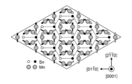
- FIG. 2 is a plan view of the crystal structure and spin structure of Mn 3 Sn.
- 1 is a graph showing an X-ray diffraction spectrum of Mn 3 Sn.
- 3A-3D are atomic force microscope (AFM) images of Mn 3 Sn samples with thicknesses of 40 nm, 25 nm, 20 nm, and 5 nm
- e-f are cross-sectional transmission electron microscope (TEM) images of Mn 3 Sn samples with thicknesses of 25 nm and 20 nm.
- FIG. 1 is a schematic diagram of Hall effect measurement.
- FIG. 1 is a graph showing the magnetic field dependence of Hall resistivity of a Mn 3 Sn sample having a film thickness of 40 nm.
- 1 is a graph showing the magnetic field dependence of Hall resistivity when an Al layer having a thickness of 4 nm is formed on a Mn 3 Sn sample having a thickness of 20 nm.
- 1 is a graph showing the magnetic field dependence of normalized Hall resistivity obtained by dividing the Hall resistivity by its respective saturation value for Mn 3 Sn samples having film thicknesses of 40 nm and 20 nm.
- FIG. 2 is a schematic diagram showing a state in which isolated grains of Mn 3 Sn are electrically insulated from each other.
- FIG. 2 is a schematic diagram showing a conductive state in which isolated grains of Mn 3 Sn are electrically connected to each other via a conductive layer.
- 1 is a schematic diagram showing a configuration of a magnetic memory element having a Hall bar structure in accordance with Example 1;
- FIG. 11 is a schematic diagram showing the configuration of a magnetic memory element of an SOT-MRAM according to a second embodiment.
- FIG. 11 is a schematic diagram showing the configuration of a magnetic memory element of an STT-MRAM according to a third embodiment.
- FIG. 13 is a schematic diagram showing the configuration of a photonic spin register according to Example 4.
- FIG. 13 is a schematic diagram showing the configuration of a photonic spin register according to a fifth embodiment.
- FIG. 13 is a schematic diagram showing the configuration of a photonic spin register according to Example 6.
- an antiferromagnet is used instead of a ferromagnet to realize a nonvolatile memory that can operate at high speed.
- the reason is that the spin response speed of an antiferromagnet is in the THz range (picoseconds), which is two to three orders of magnitude faster than that of a ferromagnet, and because the interaction between magnetic materials is small, there is a possibility that magnetic devices can be made even faster and more highly integrated.
- the object is particularly an antiferromagnetic material that has an antiferromagnetic order with macroscopically broken time reversal symmetry and exhibits an anomalous Hall effect.
- antiferromagnetic materials include antiferromagnetic metals containing manganese (Mn) and collinear antiferromagnetic materials (e.g., RuO 2 , Mn 5 Si 3 , CrSb).
- gamma Mn alloys include Mn 1-x Fe x , Mn 1-x Rh x , and Mn 1-x Pd x .
- Mn 3 Sn as an example of an antiferromagnetic material that exhibits the anomalous Hall effect will be described with reference to FIGS. 1A and 1B.
- Mn 3 Sn is an antiferromagnetic material that has a crystal structure called a kagome lattice based on a triangle, and has a structure in which the kagome lattice is stacked in the c-axis [0001] direction as shown in Figures 1A and 1B.
- Mn located at the vertices of the kagome lattice has a non-collinear chiral spin structure in which the magnetic moments (directions of localized spins) are inclined 120 degrees to each other at temperatures below 420 K due to geometric frustration.
- Three types of six-spin units arranged on a two-layer kagome lattice form a spin order called a cluster magnetic octupole, shown as a hexagon.
- This non-collinear magnetic structure can be regarded as a ferromagnetic order of cluster magnetic octupole. This ferromagnetic order breaks time-reversal symmetry macroscopically.
- the cluster magnetic octopole corresponds to the orientation of Weyl points, which are topological electronic structures, and a virtual magnetic field in momentum space (equivalent to 100 to 1000 Tesla (T) in real space), and the response derived from the Weyl points and virtual magnetic field can be controlled by the orientation of the cluster magnetic octopole.
- the magnetic structure shown in Figures 1A and 1B has orthorhombic symmetry, with only one of the three magnetic moments of Mn located at the vertices of the triangle being parallel to the easy axis of magnetization.
- the other two magnetic moments are canted with respect to the easy axis of magnetization, which is thought to induce a weak ferromagnetic moment.
- An antiferromagnet with a canted magnetic moment and thus tiny magnetization is called a canted antiferromagnet.
- a DC magnetron sputtering method can be used to prepare the Mn 3 Sn sample.
- a Mn 3 Sn film is formed from a Mn 2.7 Sn target on a thermally oxidized Si substrate at a high temperature of 500° C.
- a cap layer made of aluminum (Al) is formed in situ on the Mn 3 Sn film at room temperature.
- the method of preparing the Mn 3 Sn sample is not limited to the above-mentioned method, and other preparation methods can also be adopted.
- the crystal structure of the Mn3Sn film can be investigated using X-ray diffraction.
- the X-ray diffraction spectrum obtained by 2 ⁇ / ⁇ scanning shows the same peaks as those of D0 19 type Mn 3 Sn and Si/SiO 2 substrate, which indicates that the Mn 3 Sn film is a single phase of D0 19 type Mn 3 Sn.
- the peak intensity ratio is almost consistent with the simulation result.
- AFM atomic force microscope
- samples with t ⁇ 25 nm are conductive due to their continuous structure, while samples with t ⁇ 20 nm are electrically insulating due to their discontinuous structure.
- AFM images c and d, and TEM image f show that the average grain size of the first grains is in the range of 20 nm to 200 nm, and that within the first grains there are multiple second grains whose average grain size is less than half that of the first grains, more specifically, in the range of 1/20 to 1/2.
- a magnetic field H is applied in the direction perpendicular to the surface of the antiferromagnetic layer 2 (z direction), and a current I is passed in the longitudinal direction (x direction), and a Hall voltage Vy is measured that is generated in the y direction perpendicular to both the current I and the magnetic field H.
- the longitudinal resistivity ⁇ xx and the Hall resistivity ⁇ yx are defined as ( Vx /I) ⁇ (wt/l) and ( Vy /I) ⁇ t, respectively.
- Fig. 5A shows that a clear hysteresis loop appears, and the magnitude of ⁇ yx at zero magnetic field is about 1.3 ⁇ cm, and the coercivity is about 0.6 T.
- the anomalous Hall effect appears in the Mn 3 Sn sample.
- an antiferromagnetic layer 2 having a plurality of isolated grains of Mn 3 Sn is laminated on a substrate 1, and these isolated grains are covered with a cap layer of Al with a thickness of 2 nm.
- This cap layer is oxidized to become an oxide film 3, so that the spaces between the isolated grains are electrically insulated. In such an insulating state, the Hall effect cannot be measured.
- the thickness of the cap layer is increased so that part of the cap layer remains as the conductive layer 4, and the isolated grains are electrically connected via the conductive layer 4.
- the thickness of the Al cap layer is set to 4 nm, the surface 2 nm becomes the oxide film 3, but the antiferromagnetic layer 2 and the 2 nm on the substrate 1 side remain as the conductive layer 4.
- the linear behavior in FIG. 5B also indicates that the normal Hall effect of the Al conductive layer 4 is manifested.
- the antiferromagnetic material targeted in this embodiment has a characteristic nanoscale microstructure and exhibits a stable magnetic effect, making it applicable to magnetic memory elements.
- Example 1 targets a magnetic memory element with a Hall bar structure (see Figure 7)
- Examples 2 and 3 target a magnetic memory element having a magnetoresistance element (see Figures 8 and 9)
- Examples 4 to 6 target a photonic spin register into which data corresponding to an optical signal can be written (see Figures 10 to 12).
- one or more first grains correspond to one bit of information.
- FIG. 7 shows the configuration of a magnetic memory element 100 according to the first embodiment.
- the magnetic memory element 100 includes a substrate 10, a spin Hall layer 12 stacked on the substrate 10, and an antiferromagnetic layer 14 in contact with the spin Hall layer 12.
- the substrate 10 is made of an insulator such as MgO or SiO 2.
- the spin Hall layer 12 is made of a material exhibiting the spin Hall effect (hereinafter, spin Hall material), for example, a non-magnetic heavy metal such as tantalum (Ta), tungsten (W), or platinum (Pt), or a chalcogenide material such as a topological insulator.
- the antiferromagnetic layer 14 is a polycrystalline thin film of an antiferromagnetic material exhibiting the anomalous Hall effect as described above, and has one or more first grains with an average grain size in the range of 20 nm to 200 nm, and each first grain has a plurality of second grains with an average grain size of 1/2 or less of the first grain. In particular, it is more preferable that the average grain size of the second grains is in the range of 1/20 to 1/2 of the first grain.
- Electrodes 16a and 16b are arranged at both ends of the magnetic memory element 100 in the longitudinal direction (x direction), and electrodes 18a and 18b are arranged in the transverse direction (y direction).
- electrodes 16a and 16b and electrodes 18a and 18b are made of Au/Ti.
- a write current I write pulse current
- SOT spin-orbit torque
- the direction of the magnetic order of the antiferromagnetic layer 14 can be controlled by the direction of the write current I write .
- the magnetic order is reversed from the +z direction ("1") to the -z direction ("0")
- the magnetic order is reversed from the -z direction ("0") to the +z direction ("1").
- a read current I read (DC) is passed in the x direction through the antiferromagnetic layer 14 between the electrodes 16a and 16b.
- This causes a Hall voltage VH to be detected between the electrodes 18a and 18b due to the anomalous Hall effect.
- the sign of the Hall voltage VH is determined by the z component of the magnetic order of the antiferromagnetic layer 14. For example, when the magnetic order of the antiferromagnetic layer 14 is oriented in the +z direction, it corresponds to "1", and when it is oriented in the -z direction, it corresponds to "0".
- the magnetic memory element 100 shown in FIG. 7 a configuration in which the spin Hall layer 12 is laminated on the antiferromagnetic layer 14 (substrate/antiferromagnetic layer/spin Hall layer) may be adopted. Also, the antiferromagnetic layer 14 may be sandwiched between two spin Hall layers made of spin Hall materials having spin Hall angles of different signs.
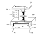
- FIG. 8 shows the configuration of a magnetic memory element 200 of a SOT-MRAM according to Example 2.
- the magnetic memory element 200 includes a magnetoresistance element 210, a spin Hall layer 220, a first terminal 231, a second terminal 232, a third terminal 233, and transistors Tr1 and Tr2.
- the spin Hall layer 220 is made of a spin Hall material, similar to the spin Hall layer 12 in FIG. 7.
- the magnetoresistance element 210 is in contact with the spin Hall layer 220 and comprises a free layer 212, which is an antiferromagnetic layer whose magnetic order (magnetization) is reversible, a non-magnetic layer 214 stacked on the free layer 212, and a reference layer 216 stacked on the non-magnetic layer 214 and whose magnetic order is fixed in the in-plane or perpendicular to the plane.
- FIG. 8 shows the case where the magnetic order of the free layer 212 and the reference layer 216 is perpendicular to the plane.
- the free layer 212 is made of an antiferromagnetic material that exhibits the anomalous Hall effect, similar to the antiferromagnetic layer 14 of FIG. 7 described above.
- the nonmagnetic layer 34 is made of an insulator (e.g., MgO, AlOx, or MgAl2O4 ).
- the reference layer 216 is made of a ferromagnetic material (e.g., CoFeB ).
- the reference layer 216 may be made of the same antiferromagnetic material as the free layer 212, in which case the antiferromagnetic material of the reference layer 216 has a larger coercive force than the antiferromagnetic material of the free layer 212.
- the magnetoresistance element 210 functions as a magnetic tunnel junction (MTJ) element.
- MTJ magnetic tunnel junction
- the magnetoresistance element 210 is assigned one bit of data, "0" or "1", depending on the resistance state.
- the magnetoresistance element 210 is in a low resistance state when the magnetic order of the cluster magnetic octopole of the reference layer 216 and the magnetic order of the cluster magnetic octopole of the free layer 212 are in the same direction (parallel state), and the magnetoresistance element 210 is in a high resistance state when they are in the opposite directions (antiparallel state).
- the data in the parallel state can be assigned as "0”
- the data in the antiparallel state can be assigned as "1".
- the magnetoresistance element 210 can be in a high resistance state when in the parallel state, and in a low resistance state when in the antiparallel state.
- the first terminal 231, the second terminal 232, and the third terminal 233 are made of metal.
- the first terminal 231 is connected to the reference layer 216, the second terminal 232 is connected to one end of the spin Hall layer 220, and the third terminal 233 is connected to the other end of the spin Hall layer 220.
- the first terminal 231 is connected to the ground line 240.
- the ground line 240 is set to ground voltage.
- the ground line 240 may be set to a reference voltage other than the ground voltage.
- Transistors Tr1 and Tr2 are, for example, N-channel metal oxide semiconductor (NMOS) transistors.
- the second terminal 232 is connected to the drain of transistor Tr1, and the third terminal 233 is connected to the drain of transistor Tr2.
- the gates of transistors Tr1 and Tr2 are connected to the word line WL.
- the source of transistor Tr1 is connected to the first bit line BL1, and the source of transistor Tr2 is connected to the second bit line BL2.
- the word line WL is set to a high level to turn on the transistors Tr1 and Tr2, one of the first bit line BL1 and the second bit line BL2 is set to a high level, and the other is set to a low level.
- the write current Iwrite flows in the in-plane direction of the spin Hall layer 220 between the first bit line BL1 and the second bit line BL2, generating a spin current in the perpendicular direction, and the magnetic order of the free layer 212 is reversed by the SOT, allowing data to be written.
- the data to be written can be changed depending on the direction of the write current Iwrite .
- the word line WL is set to a high level to turn on the transistors Tr1 and Tr2, one bit line (second bit line BL2) is set to a high level, and the other bit line (first bit line BL1) is opened.
- a read current I read flows from the high-level second bit line BL2 to the third terminal 233, the spin Hall layer 220, the free layer 212, the nonmagnetic layer 214, the reference layer 216, the first terminal 231, and the ground line 240.
- the resistance state of the magnetoresistance element 210 i.e., the stored data, can be determined.
- FIG. 9 shows the configuration of a magnetic memory element 300 of an STT-MRAM according to Example 3.
- the magnetic memory element 300 includes a magnetoresistance element 310, a first terminal 321, a second terminal 322, and a transistor Tr.
- the magnetoresistance element 310 includes a reference layer 316 whose magnetic order is fixed in-plane or perpendicular to the plane, a non-magnetic layer 314 stacked on the reference layer 316, and a free layer 312 stacked on the non-magnetic layer 314 and serving as an antiferromagnetic layer whose magnetic order is reversible.
- the free layer 312, the non-magnetic layer 314, and the reference layer 316 are made of the same materials as the free layer 212, the non-magnetic layer 214, and the reference layer 216 in FIG. 8, respectively.
- FIG. 9 shows a case where the magnetic order of the free layer 312 and the reference layer 316 is oriented perpendicular to the plane.
- the magnetoresistance element 310 is assigned one bit of data, "0" or "1", depending on the resistance state.
- the first terminal 321 and the second terminal 322 are made of metal.
- the free layer 312 is connected to the first terminal 321, and the reference layer 316 is connected to the second terminal 322.
- the first terminal 321 is connected to the bit line BL, and the second terminal 322 is connected to the transistor Tr.
- the transistor Tr is, for example, an NMOS transistor.
- the drain of the transistor Tr is connected to the second terminal 322, the source is connected to the source line SL, and the gate is connected to the word line WL.
- the word line WL is set to a high level to turn on the transistor Tr, and a write current I write is passed between the bit line BL and the source line SL in the perpendicular direction. This causes the magnetic order of the free layer 312 to be reversed by the spin transfer torque, allowing data to be written.
- the data to be written can be changed by changing the direction of the write current I write .
- the word line WL is set to a high level to turn on the transistor Tr, and a read current Iread is passed between the bit line BL and the source line SL.
- the resistance state of the magnetoresistance element 310 i.e., the stored data, can be determined.
- Example 2 (FIG. 8) and Example 3 (FIG. 9), examples were shown in which the magnetoresistance elements 210 and 310 were MTJ elements, but they can also function as giant magnetoresistance (GMR) elements.
- the nonmagnetic layers 214 and 314 are made of a nonmagnetic metal (conductor).
- Example 2 a structure (antiferromagnetic layer/ferromagnetic layer) in which a very thin ferromagnetic layer (e.g., CoFeB) of 1 nm or less is laminated on an antiferromagnetic layer may be used as the free layer 212, and a magnetoresistance element consisting of an antiferromagnetic layer/ferromagnetic layer/nonmagnetic layer/reference layer may be employed.
- a magnetoresistance element consisting of a reference layer/nonmagnetic layer/ferromagnetic layer/antiferromagnetic layer may be employed in Example 3 (FIG. 9).
- FIG. 10 shows the configuration of a photonic spin register 400 according to the fourth embodiment.
- the photonic spin register 400 includes an optical receiver 410 and a magnetic memory element 420.
- the magnetic memory element 420 comprises a spin Hall layer 430 and an antiferromagnetic layer 440 in contact with the spin Hall layer 430 and having a reversible magnetic order (magnetization).
- the spin Hall layer 430 is made of a spin Hall material, similar to the spin Hall layer 12 in FIG. 7.
- the antiferromagnetic layer 440 is made of an antiferromagnetic material that exhibits the anomalous Hall effect, similar to the antiferromagnetic layer 14 in FIG. 7.
- the optical receiver 410 includes an optical waveguide 412 provided on a substrate, and an optical receiver 414 connected to the optical waveguide 412 on the substrate.
- the optical receiver 414 includes a photoelectric conversion element 416, and a first metal film 418a and a second metal film 418b that sandwich the photoelectric conversion element 416, forming a plasmon waveguide.
- the photoelectric conversion element 416 is made of a dielectric (semiconductor or insulator) and is continuously connected to the optical waveguide 412.
- the width of the photoelectric conversion element 416 is narrower than the width of the optical waveguide 412, and the optical waveguide 412 has a tapered shape where the connection portion with the photoelectric conversion element 416 narrows toward the photoelectric conversion element 416.
- the narrower the width of the photoelectric conversion element 416 the greater the light confinement effect becomes, making it possible to focus light below the diffraction limit, and the stronger the interaction between the photoelectric conversion element 416 and the optical field.
- the first metal film 418a and the second metal film 418b are made of a metal such as Au or Ag.
- the second metal film 418b is connected to one end of the spin Hall layer 430.
- the first metal film 418a also functions as an electrode, and a bias voltage is applied to it.
- the other end of the spin Hall layer 430 is connected to an electrode 450, which is grounded.
- the optical signal PL propagates as a surface plasmon polariton at the interface between the photoelectric conversion element 416 and the first metal film 418a and the second metal film 418b, generating a strong electric field in the vicinity.
- a photocurrent I ph which is a pulse current, flows from the photodetector 414 to the spin Hall layer 430 by application of a bias voltage, and flows into the electrode 450.
- the photocurrent I ph is a pulse current corresponding to the optical signal PL, so that the magnetic order is reversed during a pulse width period during which a current with a current density equal to or greater than a predetermined value flows, and the magnetic order is not reversed during other periods.
- a read current (DC) in the same direction as the photocurrent I ph is passed through the antiferromagnetic layer 440. This generates a Hall voltage in a direction perpendicular to the read current due to the anomalous Hall effect, and the Hall voltage between the terminals 442a and 442b of the antiferromagnetic layer 440 is detected.
- the photonic spin register 400 can invert the magnetic order of the antiferromagnetic layer 440 in response to the photocurrent I ph from the photodetector 414, thereby realizing a high-speed optical-electrical interface utilizing spintronics.
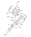
- FIG. 11 shows the configuration of a photonic spin register 500 according to the fifth embodiment.
- the photonic spin register 500 includes an optical receiver 410 and a magnetic memory element 520.
- the photonic spin register 500 has the same configuration as the photonic spin register 400 shown in FIG. 10, except that the magnetic memory element 420 is replaced with the magnetic memory element 520.
- the magnetic memory element 520 includes a spin Hall layer 530 and a magnetoresistance element 540 stacked on the spin Hall layer 530.
- the spin Hall layer 530 is made of a spin Hall material, similar to the spin Hall layer 12 in FIG. 7. One end of the spin Hall layer 530 is connected to the second metal film 418b of the photodetector 414, and the other end is connected to the electrode 450.
- the magnetoresistance element 540 is in contact with the spin Hall layer 530 and includes a free layer 542, which is an antiferromagnetic layer whose magnetic order (magnetization) is reversible, a nonmagnetic layer 544 stacked on the free layer 542, and a reference layer 546 stacked on the nonmagnetic layer 544 and whose magnetic order is fixed in-plane or perpendicular to the plane.
- the free layer 542, the nonmagnetic layer 544, and the reference layer 546 are made of the same materials as the free layer 212, the nonmagnetic layer 214, and the reference layer 216 in FIG. 8, respectively.
- the reference layer 546 is connected to a terminal 551.
- a read current is passed from the spin Hall layer 530 side toward the magnetoresistance element 540 in a direction perpendicular to the surface.
- the resistance state of the magnetoresistance element 540 i.e., the stored data, can be determined.
- the photonic spin register 500 can reverse the magnetic order of the free layer 542 in response to the photocurrent I ph from the photodetector 414, thereby realizing a high-speed optical-electrical interface utilizing spintronics.
- Example 6 focuses on a photonic spin register that uses All-Optical magnetization Switching (AOS), which reverses the magnetic order (magnetization) by irradiating an optical signal onto an antiferromagnetic layer.
- AOS All-Optical magnetization Switching
- FIG. 12 shows the configuration of a photonic spin register 600 according to Example 6.
- the photonic spin register 600 includes a light irradiation unit 610 and an antiferromagnetic layer 620 as a magnetic memory element.
- the antiferromagnetic layer 620 is made of an antiferromagnetic material that exhibits the anomalous Hall effect, similar to the antiferromagnetic layer 14 in FIG. 7.
- the light irradiating unit 610 includes a light output unit 612 and a lens 614.
- the light output unit 612 emits a light signal PL, which is an ultrashort pulse light that has been pulse-amplitude modulated.
- the light signal PL emitted from the light output unit 612 is focused in the antiferromagnetic layer 620 by the lens 614.
- the light signal PL is a pulse light
- the magnetic order of the antiferromagnetic layer 620 is reversed when light with an intensity equal to or greater than a threshold is irradiated, and the magnetic order is not reversed when light with an intensity less than the threshold is irradiated.
- the anomalous Hall effect can be used, for example, as in Examples 1 and 4 (FIGS. 7 and 10).
- the photonic spin register 600 does not require a photodetector (i.e., there is no need to convert the optical signal PL into a photocurrent), and can directly control the direction of the magnetic order in the antiferromagnetic layer 620 with light. Therefore, power consumption due to photocurrent can be completely suppressed.
- a magnetic memory device may be configured with a plurality of magnetic memory elements 100.
- a magnetic memory device may be configured with a plurality of magnetic memory elements 200 arranged in a matrix.
- a magnetic memory device may be configured with a plurality of magnetic memory elements 300 arranged in a matrix.
- a computer system or information processing system may be configured with the magnetic memory elements of Examples 1 to 3 or the photonic spin registers of Examples 4 to 6.
Landscapes
- Engineering & Computer Science (AREA)
- Computer Hardware Design (AREA)
- Hall/Mr Elements (AREA)
Priority Applications (2)
| Application Number | Priority Date | Filing Date | Title |
|---|---|---|---|
| JP2025510998A JPWO2024204298A1 (https=) | 2023-03-28 | 2024-03-27 | |
| US19/338,086 US20260096351A1 (en) | 2023-03-28 | 2025-09-24 | Magnetic memory element, magnetic memory device, photonic spin register, data writing method, data reading method, apparatus, and information processing system |
Applications Claiming Priority (2)
| Application Number | Priority Date | Filing Date | Title |
|---|---|---|---|
| JP2023052021 | 2023-03-28 | ||
| JP2023-052021 | 2023-03-28 |
Related Child Applications (1)
| Application Number | Title | Priority Date | Filing Date |
|---|---|---|---|
| US19/338,086 Continuation-In-Part US20260096351A1 (en) | 2023-03-28 | 2025-09-24 | Magnetic memory element, magnetic memory device, photonic spin register, data writing method, data reading method, apparatus, and information processing system |
Publications (1)
| Publication Number | Publication Date |
|---|---|
| WO2024204298A1 true WO2024204298A1 (ja) | 2024-10-03 |
Family
ID=92905647
Family Applications (1)
| Application Number | Title | Priority Date | Filing Date |
|---|---|---|---|
| PCT/JP2024/012153 Ceased WO2024204298A1 (ja) | 2023-03-28 | 2024-03-27 | 磁気メモリ素子、磁気メモリ装置、及びフォトニックスピンレジスタ |
Country Status (3)
| Country | Link |
|---|---|
| US (1) | US20260096351A1 (https=) |
| JP (1) | JPWO2024204298A1 (https=) |
| WO (1) | WO2024204298A1 (https=) |
Citations (4)
| Publication number | Priority date | Publication date | Assignee | Title |
|---|---|---|---|---|
| JPH10284321A (ja) * | 1997-04-03 | 1998-10-23 | Toshiba Corp | 交換結合膜とそれを用いた磁気抵抗効果素子、磁気ヘッドおよび磁気記憶装置 |
| WO2020166722A1 (ja) * | 2019-02-15 | 2020-08-20 | 国立大学法人東京大学 | スピントロニクス素子及び磁気メモリ装置 |
| WO2022158545A1 (ja) * | 2021-01-20 | 2022-07-28 | 国立大学法人東京大学 | フォトニックスピンレジスタ、情報書き込み方法、及び情報読み出し方法 |
| WO2022220251A1 (ja) * | 2021-04-12 | 2022-10-20 | 国立大学法人東京大学 | 磁気メモリ素子 |
-
2024
- 2024-03-27 JP JP2025510998A patent/JPWO2024204298A1/ja active Pending
- 2024-03-27 WO PCT/JP2024/012153 patent/WO2024204298A1/ja not_active Ceased
-
2025
- 2025-09-24 US US19/338,086 patent/US20260096351A1/en active Pending
Patent Citations (4)
| Publication number | Priority date | Publication date | Assignee | Title |
|---|---|---|---|---|
| JPH10284321A (ja) * | 1997-04-03 | 1998-10-23 | Toshiba Corp | 交換結合膜とそれを用いた磁気抵抗効果素子、磁気ヘッドおよび磁気記憶装置 |
| WO2020166722A1 (ja) * | 2019-02-15 | 2020-08-20 | 国立大学法人東京大学 | スピントロニクス素子及び磁気メモリ装置 |
| WO2022158545A1 (ja) * | 2021-01-20 | 2022-07-28 | 国立大学法人東京大学 | フォトニックスピンレジスタ、情報書き込み方法、及び情報読み出し方法 |
| WO2022220251A1 (ja) * | 2021-04-12 | 2022-10-20 | 国立大学法人東京大学 | 磁気メモリ素子 |
Also Published As
| Publication number | Publication date |
|---|---|
| US20260096351A1 (en) | 2026-04-02 |
| JPWO2024204298A1 (https=) | 2024-10-03 |
Similar Documents
| Publication | Publication Date | Title |
|---|---|---|
| US8755222B2 (en) | Bipolar spin-transfer switching | |
| JP4874884B2 (ja) | 磁気記録素子及び磁気記録装置 | |
| US7120049B2 (en) | Magnetic cell and magnetic memory | |
| KR100439288B1 (ko) | 자기저항 효과 메모리 셀에 정보를 기입하거나 판독하는방법 | |
| JP6063381B2 (ja) | 書込み可能な磁気素子 | |
| JP5634422B2 (ja) | 電流によって誘起されたスピンモーメント移行をベースとした高速かつ低電力の磁気デバイス | |
| US6730949B2 (en) | Magnetoresistance effect device | |
| JP7710752B2 (ja) | 磁気メモリ素子及びその作製方法 | |
| US20210012940A1 (en) | Magnetic memory structures using electric-field controlled interlayer exchange coupling (iec) for magnetization switching | |
| JP5318191B2 (ja) | 磁気メモリ | |
| JP5166600B2 (ja) | トンネル磁気記録素子、磁気メモリセル及び磁気ランダムアクセスメモリ | |
| JP2014502423A (ja) | 双極性スピン転移反転 | |
| WO2013080436A1 (ja) | 記憶素子、記憶装置 | |
| TWI422083B (zh) | Magnetic memory lattice and magnetic random access memory | |
| CN100433181C (zh) | 磁存储器以及写该磁存储器的方法 | |
| JP7784762B2 (ja) | 磁気メモリ素子、情報処理システム、及び磁気メモリ素子の制御方法 | |
| WO2024204298A1 (ja) | 磁気メモリ素子、磁気メモリ装置、及びフォトニックスピンレジスタ | |
| WO2024095960A1 (ja) | 磁気メモリ素子及び磁気メモリ装置 | |
| JP2011253884A (ja) | 磁気記憶装置 | |
| JP5374589B2 (ja) | 磁気メモリ | |
| WO2024150833A1 (ja) | 磁気抵抗効果素子および磁気メモリ装置 | |
| WO2013080437A1 (ja) | 記憶素子、記憶装置 |
Legal Events
| Date | Code | Title | Description |
|---|---|---|---|
| 121 | Ep: the epo has been informed by wipo that ep was designated in this application |
Ref document number: 24780404 Country of ref document: EP Kind code of ref document: A1 |
|
| ENP | Entry into the national phase |
Ref document number: 2025510998 Country of ref document: JP Kind code of ref document: A |
|
| WWE | Wipo information: entry into national phase |
Ref document number: 2025510998 Country of ref document: JP |
|
| NENP | Non-entry into the national phase |
Ref country code: DE |
|
| 122 | Ep: pct application non-entry in european phase |
Ref document number: 24780404 Country of ref document: EP Kind code of ref document: A1 |