WO2024203689A1 - フィラー配列フィルム及びその製造方法並びに接続構造体及びその製造方法 - Google Patents
フィラー配列フィルム及びその製造方法並びに接続構造体及びその製造方法 Download PDFInfo
- Publication number
- WO2024203689A1 WO2024203689A1 PCT/JP2024/010941 JP2024010941W WO2024203689A1 WO 2024203689 A1 WO2024203689 A1 WO 2024203689A1 JP 2024010941 W JP2024010941 W JP 2024010941W WO 2024203689 A1 WO2024203689 A1 WO 2024203689A1
- Authority
- WO
- WIPO (PCT)
- Prior art keywords
- filler
- film
- resin layer
- insulating resin
- fillers
- Prior art date
- Legal status (The legal status is an assumption and is not a legal conclusion. Google has not performed a legal analysis and makes no representation as to the accuracy of the status listed.)
- Ceased
Links
Images


Classifications
-
- H—ELECTRICITY
- H01—ELECTRIC ELEMENTS
- H01R—ELECTRICALLY-CONDUCTIVE CONNECTIONS; STRUCTURAL ASSOCIATIONS OF A PLURALITY OF MUTUALLY-INSULATED ELECTRICAL CONNECTING ELEMENTS; COUPLING DEVICES; CURRENT COLLECTORS
- H01R11/00—Individual connecting elements providing two or more spaced connecting locations for conductive members which are, or may be, thereby interconnected, e.g. end pieces for wires or cables supported by the wire or cable and having means for facilitating electrical connection to some other wire, terminal, or conductive member, blocks of binding posts
- H01R11/01—Individual connecting elements providing two or more spaced connecting locations for conductive members which are, or may be, thereby interconnected, e.g. end pieces for wires or cables supported by the wire or cable and having means for facilitating electrical connection to some other wire, terminal, or conductive member, blocks of binding posts characterised by the form or arrangement of the conductive interconnection between the connecting locations
-
- C—CHEMISTRY; METALLURGY
- C08—ORGANIC MACROMOLECULAR COMPOUNDS; THEIR PREPARATION OR CHEMICAL WORKING-UP; COMPOSITIONS BASED THEREON
- C08K—Use of inorganic or non-macromolecular organic substances as compounding ingredients
- C08K3/00—Use of inorganic substances as compounding ingredients
- C08K3/01—Use of inorganic substances as compounding ingredients characterized by their specific function
- C08K3/013—Fillers, pigments or reinforcing additives
-
- C—CHEMISTRY; METALLURGY
- C08—ORGANIC MACROMOLECULAR COMPOUNDS; THEIR PREPARATION OR CHEMICAL WORKING-UP; COMPOSITIONS BASED THEREON
- C08L—COMPOSITIONS OF MACROMOLECULAR COMPOUNDS
- C08L101/00—Compositions of unspecified macromolecular compounds
-
- H—ELECTRICITY
- H01—ELECTRIC ELEMENTS
- H01B—CABLES; CONDUCTORS; INSULATORS; SELECTION OF MATERIALS FOR THEIR CONDUCTIVE, INSULATING OR DIELECTRIC PROPERTIES
- H01B5/00—Non-insulated conductors or conductive bodies characterised by their form
- H01B5/16—Non-insulated conductors or conductive bodies characterised by their form comprising conductive material in insulating or poorly conductive material, e.g. conductive rubber
-
- H—ELECTRICITY
- H01—ELECTRIC ELEMENTS
- H01R—ELECTRICALLY-CONDUCTIVE CONNECTIONS; STRUCTURAL ASSOCIATIONS OF A PLURALITY OF MUTUALLY-INSULATED ELECTRICAL CONNECTING ELEMENTS; COUPLING DEVICES; CURRENT COLLECTORS
- H01R43/00—Apparatus or processes specially adapted for manufacturing, assembling, maintaining, or repairing of line connectors or current collectors or for joining electric conductors
-
- H—ELECTRICITY
- H05—ELECTRIC TECHNIQUES NOT OTHERWISE PROVIDED FOR
- H05K—PRINTED CIRCUITS; CASINGS OR CONSTRUCTIONAL DETAILS OF ELECTRIC APPARATUS; MANUFACTURE OF ASSEMBLAGES OF ELECTRICAL COMPONENTS
- H05K1/00—Printed circuits
- H05K1/02—Details
- H05K1/03—Use of materials for the substrate
-
- H—ELECTRICITY
- H05—ELECTRIC TECHNIQUES NOT OTHERWISE PROVIDED FOR
- H05K—PRINTED CIRCUITS; CASINGS OR CONSTRUCTIONAL DETAILS OF ELECTRIC APPARATUS; MANUFACTURE OF ASSEMBLAGES OF ELECTRICAL COMPONENTS
- H05K1/00—Printed circuits
- H05K1/02—Details
- H05K1/03—Use of materials for the substrate
- H05K1/0313—Organic insulating material
- H05K1/0353—Organic insulating material consisting of two or more materials, e.g. two or more polymers, polymer + filler, + reinforcement
- H05K1/0373—Organic insulating material consisting of two or more materials, e.g. two or more polymers, polymer + filler, + reinforcement containing additives, e.g. fillers
-
- H—ELECTRICITY
- H10—SEMICONDUCTOR DEVICES; ELECTRIC SOLID-STATE DEVICES NOT OTHERWISE PROVIDED FOR
- H10H—INORGANIC LIGHT-EMITTING SEMICONDUCTOR DEVICES HAVING POTENTIAL BARRIERS
- H10H20/00—Individual inorganic light-emitting semiconductor devices having potential barriers, e.g. light-emitting diodes [LED]
- H10H20/80—Constructional details
- H10H20/85—Packages
- H10H20/857—Interconnections, e.g. lead-frames, bond wires or solder balls
-
- H—ELECTRICITY
- H10—SEMICONDUCTOR DEVICES; ELECTRIC SOLID-STATE DEVICES NOT OTHERWISE PROVIDED FOR
- H10W—GENERIC PACKAGES, INTERCONNECTIONS, CONNECTORS OR OTHER CONSTRUCTIONAL DETAILS OF DEVICES COVERED BY CLASS H10
- H10W72/00—Interconnections or connectors in packages
- H10W72/071—Connecting or disconnecting
Definitions
- the present invention relates to a filler array film and its manufacturing method, as well as a connection structure and its manufacturing method.
- ⁇ LEDs micro light emitting diodes
- ⁇ LEDs typically have a pair of electrodes arranged on one side, but they are tiny electronic components with a fine pitch that means the space between the electrodes is extremely narrow.
- anisotropic conductive films applicable to ⁇ LEDs there have been proposed a film in which a group of conductive particles consisting of multiple conductive particles is regularly arranged at a distance from each other over the entire surface of an insulating resin sheet (Patent Document 1), and a filler-arranged film that can function as an anisotropic conductive film that has been diced into microLED-sized pieces by the so-called laser lift-off method (Patent Document 2).
- the present invention seeks to solve the problems of the past, and aims to provide a structure to the filler array film required for the creation of an image display device in which a large number of fine optical elements, such as a ⁇ LED display, are arranged on a display substrate, using a filler array film that can function as an anisotropic conductive film, which does not require a singulation process such as the laser lift-off method described above, and can be formed using a simple transfer mold.
- ⁇ LEDs as an example, but the present invention can achieve the same effects even with optical elements that can be determined to be larger than ⁇ LEDs (mini LEDs). It can also be applied to microscopic components other than optical elements.
- the object of the present invention can be achieved by providing preferably a plurality of recesses and protrusions on one side of the insulating resin layer for retaining filler of a filler-arranged film having an insulating resin layer for retaining filler and a filler, and arranging a filler group consisting of a plurality of fillers on the protrusions, and thus completed the present invention.
- the present invention is a filler-arranged film having a filler-retaining insulating resin layer and a filler, A recess and a protrusion are formed on one side of the filler-holding insulating resin layer,
- the present invention provides a filler-arranged film in which at least one filler group consisting of a plurality of fillers is arranged on the convex portion.
- Each filler constituting the filler group is preferably arranged on the top surface of the convex portion or in a state where at least a part of the filler is embedded in the filler-retaining insulating resin layer constituting the convex portion.
- the convex portions are regularly arranged, and it is preferable that a plurality of fillers are regularly arranged in the filler group. It is also preferable that no filler is arranged in the concave portion.
- Such a concave portion may penetrate the filler-retaining insulating resin layer.
- Another insulating resin layer may be laminated on at least one side of the filler-retaining insulating resin layer, and in that case, the convex portion may be separated from the other convex portions by the penetrating concave portion.
- another insulating resin layer may be laminated. As the other insulating resin layer laminated in this way, an insulating resin layer for forming a black matrix can be preferably adopted.
- the present invention also relates to a method for producing the filler array film of the present invention, comprising the steps of: (Step A) A step of forming a filler-retaining insulating resin layer on a release film that has been subjected to a release treatment; (Process B) A step of forming recesses and protrusions on one side of the insulating resin layer for retaining the filler by contacting a pressing mold having recesses corresponding to the protrusions of the filler arrangement film with the insulating resin layer for retaining the filler and performing heat pressing; and (step C).
- the present invention provides a method for producing a filler-arranged film having the above structure.
- step C is followed by the following step D: (Step D) a step of embedding each of the fillers transferred onto the top surfaces of the protrusions in a filler-holding insulating resin layer so that at least a portion of each of the fillers is embedded; It is preferred that the compound has the formula:
- the present invention provides a connection structure in which a second article is connected to a first article via the above-mentioned filler-arranged film of the present invention.
- the second article corresponds to the convex portion of the filler-arranged film (preferably in one-to-one correspondence).
- the first article is a transparent display substrate having a transparent electrode arranged on one side
- the second article is a ⁇ LED having an electrode formed on one side
- the filler arranged on the convex portion of the filler-arranged film is a conductive particle
- the filler-arranged film itself functions as a conductive film or an anisotropic conductive film.
- the present invention also provides a method for manufacturing a connection structure, characterized in that the above-mentioned filler-arranged film of the present invention is sandwiched between a first article and a second article, preferably so that the second article and the convex portion of the filler-arranged film correspond (preferably one-to-one), and then pressure-bonded, for example, by thermo-pressing.
- the first article is a transparent display substrate having a transparent electrode arranged on one side
- the second article is a ⁇ LED having an electrode formed on one side
- the filler arranged on the convex portion of the filler-arranged film is a conductive particle
- the filler-arranged film itself functions as a conductive film or an anisotropic conductive film.
- the filler-arranged film may be described using an anisotropic conductive film as an example, but the contents of the description can also be applied to the case where a conductive film is used as an example.
- a conductive film instead of ⁇ LEDs, other minute light-emitting elements such as mini-LEDs or minute components (electronic components) can also be applied as the second article to be targeted.
- An example of the size of the second article is one having a maximum length of one side of 200 ⁇ m or less. It may also be 10 to 30 ⁇ m square, which is extremely difficult to handle manually.
- the filler-arranged film of the present invention has an insulating resin layer for holding fillers and a filler, and preferably has a plurality of recesses and protrusions on one side of the insulating resin layer for holding fillers. At least one filler group consisting of a plurality of fillers is arranged on each protrusion.
- the protrusions can be made to basically correspond one-to-one with the microelectronic components such as ⁇ LEDs to be connected with the filler-arranged film.
- the filler can be transferred only to the top surface of the protrusions from a filler transfer sheet in which the fillers are regularly arranged, while no filler is arranged on the bottom of the recesses.
- the protrusions of the filler-arranged film can function as individual pieces of the filler-arranged film to achieve anisotropic conductive connection without worrying about short circuits.
- a thin insulating resin layer can be left on the recesses, there is also the advantage that the protrusions are less likely to fall off the filler-arranged film during handling.
- a press mold having recesses corresponding to the protrusions of the filler-arranged film is brought into contact with the insulating resin layer for retaining the filler and heat pressed to form multiple recesses and protrusions on one side of the insulating resin layer for retaining the filler. Therefore, the planar shape and surface area of the top surface of the protrusions of the filler-arranged film, and the cross-sectional shape and height of the protrusions can be relatively easily formed by the press mold. Moreover, since there is no need to create fine holes in the press mold for regularly arranging the minute fillers, the press mold can be made at low cost.
- the filler in the manufacturing method of the filler-arranged film of the present invention, can be transferred only to the protrusions formed by the press mold using a conventional filler transfer sheet in which the filler is arranged all over the surface. In other words, even if the arrangement of the filler group in the filler-arranged film is changed, it is only necessary to make a new press mold, which can be made relatively easily and at low cost.
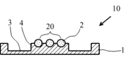
- FIG. 1A is a schematic cross-sectional view of a filler array film of the present invention.
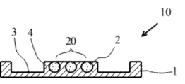
- FIG. 1B is a schematic cross-sectional view of the filler array film of the present invention.
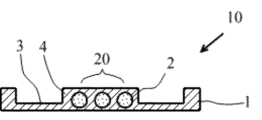
- FIG. 1C is a schematic cross-sectional view of the filler array film of the present invention.
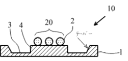
- FIG. 1D is a schematic cross-sectional view of a filler array film of the present invention.
- FIG. 2 is a schematic cross-sectional view of a filler array film of the present invention.
- FIG. 3 is a schematic cross-sectional view of a filler array film of the present invention.
- FIG. 4 is a schematic cross-sectional view of a filler array film of the present invention.
- FIG. 1A is a schematic cross-sectional view of a filler array film of the present invention.
- FIG. 1B is a schematic cross-sectional view of the filler array film of the present invention.
- FIG. 1C is a schematic cross-sectional view of the filler
- FIG. 5 is a schematic cross-sectional view of a filler array film of the present invention.
- FIG. 6 is an explanatory diagram of a filler group on the top surface of a convex portion of the filler arranged film of the present invention.
- FIG. 7 is an explanatory diagram of a filler group on the top surface of a convex portion of a filler-arranged film of the present invention.
- FIG. 8 is a schematic cross-sectional view of another embodiment of the filler arrangement film of the present invention.
- FIG. 9A is a schematic cross-sectional view of another embodiment of the filler array film of the present invention.
- FIG. 9B is a schematic cross-sectional view of another embodiment of the filler array film of the present invention.
- FIG. 9C is a schematic cross-sectional view of another embodiment of the filler array film of the present invention.
- FIG. 10 is a schematic cross-sectional view of another embodiment of the filler array film of the present invention.
- FIG. 11 is a process explanatory diagram of the method for producing a filler arranged film of the present invention.
- FIG. 12 is a process explanatory diagram of the method for producing a filler arranged film of the present invention.
- FIG. 13 is a process explanatory diagram of the method for producing the filler arranged film of the present invention.
- FIG. 14 is a process explanatory diagram of the method for producing the filler arranged film of the present invention.
- FIG. 15 is a process explanatory diagram of the method for producing the filler arranged film of the present invention.
- FIG. 16 is a process explanatory diagram of the method for producing a filler arranged film of the present invention.
- FIG. 17A is a schematic cross-sectional view of a filler array film obtained by steps A to C of the filler array film manufacturing method of the present invention.
- FIG. 17B is a schematic cross-sectional view of the filler array film obtained by steps A to D of the filler array film manufacturing method of the present invention.
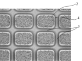
- FIG. 18 is an optical microscope photograph of the convex portion side surface of the filler arranged film of the present invention.
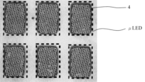
- FIG. 19 is a partially enlarged photograph of an anisotropic conductive film produced using a stamping die.
- FIG. 20 is a partially enlarged photograph of an anisotropic conductive film produced using a stamping die.
- FIG. 21 is a diagram showing the wiring pattern of the glass substrate of the connection structure for insulating property evaluation.
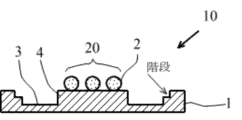
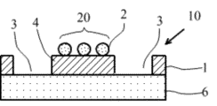
- the filler array film 10 of the present invention has a filler retaining insulating resin layer 1 and a filler 2.
- a recess 3 and a protrusion 4 are preferably formed on one side of the filler retaining insulating resin layer 1.
- the protrusion 4 is a portion for retaining the filler 2, and at least one filler group 20 consisting of a plurality of fillers 2 is arranged on the protrusion 4.
- the filler 2 constituting the filler group 20 is arranged on the top surface of the protrusion 4, but as shown in FIGS.
- each filler 2 constituting the filler group 20 may be arranged so that at least a part of it is embedded in the filler retaining insulating resin layer 1 constituting the protrusion 4.
- the filler 2 in FIG. 1B, almost half of the particle diameter of the filler 2 is embedded in the filler retaining insulating resin layer 1, in FIG. 1C, the end of the filler 2 is embedded so as to be flush with the filler retaining insulating resin layer 1, and in FIG. 1D, the filler 2 is completely embedded without being exposed in the filler retaining insulating resin layer 1.
- each convex portion functions substantially as a piece-like filler-arranged film. Therefore, when the filler is a conductive particle, the filler-arranged film can function substantially as a piece-like conductive film or an anisotropic conductive film.
- the "arrangement" in the filler array film has two meanings.
- One meaning is that the convex portions 4 rising from the concave portions 3 themselves are arranged randomly or in a regular arrangement (e.g., a square lattice arrangement, a hexagonal lattice arrangement, etc., but not limited to a lattice arrangement), as shown in FIG. 1A.
- the other meaning is that the filler 2 in the filler group 20 arranged in the convex portions 4 itself is arranged randomly or in a regular arrangement (e.g., a square lattice arrangement, a hexagonal lattice arrangement, etc.). From the viewpoint of filler capture and manufacturing costs, it is preferable that the arrangement of the convex portions 4 and the arrangement of the filler 2 are each in a regular arrangement (particularly a hexagonal lattice arrangement).
- the filler-retaining insulating resin layer 1 constituting the filler array film 10 of the present invention can have the same configuration as the insulating resin layer that retains the filler in the conventional anisotropic conductive film or conductive film, and can be formed, for example, from a thermosetting resin composition.
- a thermosetting resin composition preferably contains a rubber component, a film-forming resin, a thermosetting resin, a thermosetting agent, and an inorganic filler. This inorganic filler is different from the filler arranged in the convex portion 4, and is uniformly dispersed in the filler-retaining insulating resin layer 1.
- the filler-retaining insulating resin layer 1 can contain other known additives as necessary within a range that does not impair the effects of the invention.
- the layer thickness of the filler-retaining insulating resin layer 1 can be appropriately determined depending on the shape and surface area of the concave portion 3 and the convex portion 4, but is preferably equal to or greater than the average particle diameter of the filler 2 and not greater than two times. If the layer thickness is too thick, there is a concern that the bottom thickness of the concave portion 3 will not be thin, and the filler may be arranged in the concave portion 3, or the light transmittance of the concave portion 3 may be reduced.
- the filler-retaining insulating resin layer 1 is one that functions as an adhesive film or connection film having adhesiveness, such as a general anisotropic conductive film.
- the rubber component contained in the thermosetting resin composition is a component for imparting cushioning (shock absorption) to the filler-retaining insulating resin layer, and is not particularly limited as long as it is an elastomer with good cushioning properties.
- Specific examples include acrylic rubber, silicone rubber, butadiene rubber, and polyurethane resin (polyurethane-based elastomer). Among these, it is preferable to use one or more selected from acrylic rubber and silicone rubber.
- the content of the rubber component is preferably 1 part by mass or more, more preferably 2 parts by mass or more, and preferably 20 parts by mass or less, and more preferably 10 parts by mass or less, relative to 100 parts by mass of the total of the rubber component, the film-forming resin, the thermosetting resin, the thermosetting agent, and the inorganic filler.
- phenoxy resin From the viewpoint of film-forming properties, various resins such as phenoxy resin, polyester resin, polyurethane resin, polyester urethane resin, acrylic resin, polyimide resin, butyral resin, etc., preferably having a weight average molecular weight of about 10,000 to 80,000, may be used alone or in combination of two or more. Among these, it is preferable to use phenoxy resin from the viewpoint of film formation state, connection reliability, etc.
- the content of the film-forming resin is preferably 20 parts by mass or more, more preferably 25 parts by mass or more, even more preferably 35 parts by mass or more, preferably 50 parts by mass or less, more preferably 45 parts by mass or less, and even more preferably 40 parts by mass or less, relative to 100 parts by mass of the total of the rubber component, the film-forming resin, the thermosetting resin, the thermosetting agent, and the inorganic filler.
- thermosetting resin examples include epoxy compounds and (meth)acrylate compounds, and epoxy compounds are particularly preferred. These compounds may be monomers, oligomers, or polymers.
- the content of the thermosetting resin is preferably 10 parts by mass or more, more preferably 20 parts by mass or more, preferably 50 parts by mass or less, more preferably 40 parts by mass or less, and even more preferably 35 parts by mass or less, relative to 100 parts by mass of the total of the rubber component, the film-forming resin, the thermosetting resin, the thermosetting agent, and the inorganic filler.
- Epoxy compounds that can be used as thermosetting resins are not particularly limited as long as they have one or more epoxy groups in the molecule, and may be, for example, bisphenol A type epoxy resins, bisphenol F type epoxy resins, or urethane-modified epoxy resins. Among these, high-purity bisphenol A type epoxy resins can be preferably used.
- a specific example of high-purity bisphenol A type epoxy resin is the product name "YL980" manufactured by Mitsubishi Chemical Corporation.
- the content of the epoxy compound is preferably 30 parts by mass or more, more preferably 35 parts by mass or more, preferably 60 parts by mass or less, more preferably 55 parts by mass or less, and even more preferably 45 parts by mass or less, per 100 parts by mass of the total of the rubber component, the film-forming resin, the thermosetting resin, the thermosetting agent, and the inorganic filler.
- thermosetting agent is selected according to the thermosetting resin.
- thermosetting resin is an epoxy compound
- a thermal anionic polymerization initiator or a thermal cationic polymerization initiator can be preferably selected, and a thermal cationic polymerization initiator that can suppress the curing reaction caused by laser light and rapidly cure by heat can be more preferably selected.
- the content of the thermosetting agent can be determined according to the type of the thermosetting agent and the type of the thermosetting resin.
- the content of the thermosetting agent is preferably 1 part by mass or more, more preferably 2 parts by mass or more, even more preferably 3 parts by mass or more, preferably 10 parts by mass or less, more preferably 8 parts by mass or less, and even more preferably 6 parts by mass or less, based on 100 parts by mass of the total of the rubber component, the film-forming resin, the thermosetting resin, the thermosetting agent, and the inorganic filler.
- Thermal cationic polymerization initiators preferably applicable to epoxy compounds are those that generate an acid capable of cationic polymerization of cationic polymerizable compounds by heat, and known iodonium salts, sulfonium salts, phosphonium salts, ferrocenes, etc. can be used. Among these, aromatic sulfonium salts that show good latency against temperature can be preferably used.
- aromatic sulfonium salt-based polymerization initiator is San-Aid SI-60L manufactured by Sanshin Chemical Industry Co., Ltd.
- the content of such thermal cationic polymerization initiator is preferably 1 part by mass or more, more preferably 2 parts by mass or more, even more preferably 3 parts by mass or more, preferably 15 parts by mass or less, more preferably 10 parts by mass or less, and even more preferably 8 parts by mass or less, per 100 parts by mass of the total of the rubber component, the film-forming resin, the thermosetting resin, the thermosetting agent, and the inorganic filler.
- the inorganic filler in the thermosetting resin composition is used for the purpose of adjusting the durometer A hardness, storage modulus at a frequency of 200 Hz, and storage modulus after curing of the filler-retaining insulating resin layer 1, and may be silica filler, talc filler, titanium oxide filler, calcium carbonate filler, magnesium oxide filler, silane coupling agent filler, bulking agent filler, softener filler, colorant filler, flame retardant filler, thixotropic agent filler, etc.
- the inorganic filler may be used alone or in combination of two or more kinds.
- the content of the inorganic filler is preferably 1 part by mass or more, more preferably 5 parts by mass or more, even more preferably 8 parts by mass or more, preferably 20 parts by mass or less, more preferably 15 parts by mass or less, and even more preferably 12 parts by mass or less, per 100 parts by mass of the total of the rubber component, the film-forming resin, the thermosetting resin, the thermosetting agent, and the inorganic filler.
- the content of the rubber component is 2 parts by mass or more and 10 parts by mass or less, per 100 parts by mass of the total of the rubber component, the film-forming resin, the thermosetting resin, the thermosetting agent, and the inorganic filler, by setting the content of the inorganic filler to 8 parts by mass or more and 12 parts by mass or less, the desired durometer A hardness, storage modulus at a frequency of 200 Hz, and storage modulus after curing can be easily achieved.
- the protrusion 4 holds the filler 2, and preferably holds the filler 2 on its top surface or on the filler-holding insulating resin layer 1 constituting the protrusion 4.
- the protrusion 4 is preferably formed at a position corresponding to the second article. In this case, it is preferable that the second article and the protrusion 4 correspond to each other in a 1:1 relationship, but one protrusion 4 may correspond to two or more second articles.
- the planar shape and size (area) of the protrusion 4 are approximately the same as the planar shape and size of the second object to be connected or its electrode.
- the second object is a ⁇ LED
- the planar shape and size of the protrusion 4 are approximately the same as the outer shape of the ⁇ LED or the outer shape of one electrode in the ⁇ LED.
- the protrusion 4 may be a rectangle with one side of 5 ⁇ m to 100 ⁇ m, and is preferably a rectangle with one side of 10 ⁇ m to 30 ⁇ m.
- the side of the protrusion 4 rises vertically from the recess 3, but it may have a taper as shown in Figure 2, or may be stepped as shown in Figure 3.
- the planar shape and size (area) of the protrusion 4 have been described using a ⁇ LED as an example of the second object to be connected, but a relatively large object such as a mini LED can also be used as the object to be connected.
- the size of the protrusion 4 can be adjusted to match the size of the object to be connected. Even if a part has an outer shape of 100 ⁇ m or more on a side, it can be the object to be connected as long as it does not impair the effect of the invention.
- the height t 0 of the convex portion 4 corresponds to the thickness of the insulating resin layer 1 for retaining the filler.
- the height is usually preferably 1 ⁇ m or more, more preferably 2 ⁇ m or more, preferably 20 ⁇ m or less, more preferably 10 ⁇ m or less, and is preferably 1 to 2 times the average particle diameter of the filler 2.
- the component to be connected is not completely buried in the insulating resin layer 1 for retaining the filler, and a fillet can be formed on the periphery of the component. It is preferable that the planar shape, size (area), height, and relationship between the top surface of the convex portion 4 and the bottom surface of the concave portion 3 are all the same, but this is not limited thereto.
- the number density [pieces/mm 2 ] of the convex portions 4 can be appropriately selected as an optimal number density depending on the purpose of use of the filler array film, the object to be connected, etc. Generally, it is 50 [pieces/mm 2 ] or more and 10,000 [pieces/mm 2 ] or less, but when the filler array film is used as an anisotropic conductive film or a conductive film and applied to the mounting of ⁇ LEDs, it is preferably 100 [pieces/mm 2 ] or more, more preferably 300 [pieces/mm 2 ] or more, preferably 3,000 [pieces/mm 2 ] or less, and more preferably 1,500 [pieces/mm 2 ] or less. In addition, the minimum distance between the convex portions 4 is preferably 5 ⁇ m or more in order to avoid contact between the convex portions 4 that should be separated in the filler transfer process and component mounting.
- the number of fillers provided on one protrusion 4 is no particular limit to the number of fillers provided on one protrusion 4, but the lower limit is preferably 2 or more, and the upper limit is preferably 1,500 or less. Assuming that the fillers will be captured by a maximum of two electrodes provided on a component with a very small external shape, it is preferable to set the number in this range.
- the recess 3 is formed reflectively when the protrusion 4 is formed, and has the function of separating the protrusion 4 from the adjacent protrusion 4.
- the inner wall of the recess 3 is vertical and the bottom is flat, but this is not limited thereto. As shown in Figure 4, it may have a taper that widens upward, or as shown in Figure 5, it may have a stepped shape.
- the side of the protrusion 4 may be as shown in Figure 2 or Figure 3.
- the light transmittance of that part is improved, making it easier to optically distinguish it from the protrusion 4, and making it easier to handle the protrusion 4 as a substantially individual piece of filler array film 10.
- at least a portion of the bottom surface of the recess 3 may be perforated, so long as the protrusion 4 is not completely separated from the filler array film 10. This is because a protrusion 4 that has been completely perforated through the recess 3 and separated into an individual piece cannot be handled as part of the filler array film 10.
- Filler 2 As the filler 2 arranged in the convex portion 4, various fillers used in known filler-arranged films can be appropriately selected and used according to the application of the filler-arranged film (conductive film, anisotropic conductive film, adhesive film, optical film, ferromagnetic film, etc.).
- the filler 2 can be appropriately selected according to the performance required for the application, such as hardness and optical performance.
- silica fillers for example, in optical films and matte films, silica fillers, titanium oxide fillers, styrene fillers, acrylic fillers, melamine fillers, various titanate fillers, etc. can be used.
- titanium oxide filler, magnesium titanate filler, zinc titanate filler, bismuth titanate filler, lanthanum oxide filler, calcium titanate filler, strontium titanate filler, barium titanate filler, barium zirconate titanate filler, lead zirconate titanate filler, and mixtures thereof can be used.
- polymer-based rubber particles, silicone rubber particles, and the like can be contained.
- conductive film or anisotropic conductive film conductive particles are contained.
- Examples of conductive particles include metal particles such as nickel, cobalt, silver, copper, gold, and palladium, alloy particles such as solder, metal-coated resin particles, and metal-coated resin particles with insulating fine particles attached to the surface. Two or more kinds can be used in combination. Among them, metal-coated resin particles are preferred because the resin particles repel each other after connection, making it easier to maintain contact with the terminal and stabilizing the conductive performance.
- the surface of the conductive particles may be subjected to an insulating treatment by a known technique that does not impair the conductive characteristics.
- the fillers listed above for each application are not limited to the applications, and may contain fillers for other applications as necessary. In addition, in the filler-arranged film for each application, two or more fillers may be used in combination as necessary.
- the shape of the filler 2 is appropriately selected from spheres, ellipsoids, columns, needles, combinations thereof, etc., depending on the application of the filler-arranged film.
- a spherical shape is preferable because it makes it easier to check the filler arrangement and maintain a uniform state.
- the conductive particles are approximately spherical.
- sphericity calculated using the following formula is between 70 and 100.
- So is the area of the circumscribing circle of the filler in the planar image of the filler
- Si is the area of the inscribing circle of the filler in the planar image of the filler.
- planar images of the filler are taken in the surface view and cross section of the filler array film, and the areas of the circumscribed circles and the inscribed circles of any 100 or more fillers (preferably 200 or more fillers) are measured in each planar image, and the average of the circumscribed circle areas and the average of the inscribed circle areas are calculated and set as the above-mentioned So and Si.
- the sphericity is within the above range in both the surface view and the cross section.
- the difference in sphericity between the surface view and the cross section is preferably within 20, more preferably within 10.
- the difference in sphericity is small. Note that this sphericity can also be calculated using a wet flow type particle size and shape analyzer FPIA-3000 (manufactured by Malvern Panalytical) if it is a single filler.
- the average particle size of the filler is determined appropriately depending on the application of the filler array film.
- the average particle size is preferably 1 ⁇ m or more, more preferably 2.5 ⁇ m or more, preferably 30 ⁇ m or less, and more preferably 9 ⁇ m or less.
- a particle size larger than 9 ⁇ m may be appropriate.
- the average particle diameter of the filler before being placed on the convex portion 4 of the filler array film 10 can be measured by a general particle size distribution measuring device, and the average particle diameter can also be determined using a particle size distribution measuring device.
- An example of a particle size distribution measuring device is the FPIA-3000 (manufactured by Malvern Panalytical).
- the average particle diameter of the filler in the filler array film can be determined by observation with an electron microscope such as a SEM. In this case, it is desirable to measure the average particle diameter of the filler by using 200 or more samples.
- the maximum length or the diameter of a shape that resembles a sphere can be used as the average particle diameter of the filler.
- the variation in the average particle size of the filler in the filler-arranged film is set to a CV value (standard deviation/average) of 20% or less.
- CV value standard deviation/average
- the filler-arranged film is easily pressed evenly when it is pressed onto an article, and especially when the filler is arranged, it is possible to prevent the pressure from concentrating locally, which contributes to the stability of the connection.
- the connection state can be accurately evaluated by indentation after connection.
- the filler-arranged film is configured as an anisotropic conductive film
- the connection state can be accurately confirmed by indentation regardless of whether the terminal size is large (FOG, etc.) or small (COG, etc.). Therefore, it is expected that inspection after anisotropic conductive connection will be easier and the productivity of the connection process will be improved.
- the variation in average particle size can be calculated using an image-type particle size analyzer or the like.
- the average particle size of the filler not contained in the filler array film, which is used as the raw material particle of the filler array film can also be determined using the above-mentioned wet flow particle size and shape analyzer FPIA-3000 (manufactured by Malvern Panalytical). In this case, if 1000 or more fillers, preferably 3000 or more, and more preferably 5000 or more fillers are measured, the variation in particle size of the individual fillers can be accurately grasped. If the filler is arranged in the filler array film, it can be determined from a planar image or a cross-sectional image, as with the above-mentioned sphericity.
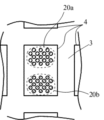
- the filler group 20 is composed of a plurality of fillers arranged on the convex portion 4 in order to enhance the capture of the filler when the second article is connected to the first article via the filler array film 10.
- at least one filler group 20 consisting of a plurality of fillers 2 is arranged on the convex portion 4. Therefore, a plurality of filler groups 20 may be arranged on one convex portion 4.
- FIG. 6 a plan view of one convex portion
- adjacent filler groups (20a and 20b) on one convex portion 4 are completely separated from each other, but as shown in FIG. 7, some fillers 2a may be common.
- FIG. 6 a plan view of one convex portion
- the separated filler groups 20a and 20b are made to correspond to the anode electrode and cathode electrode of the ⁇ LED, respectively, to prevent a short circuit from occurring between them.
- the fillers 2 in the filler group 20 may be arranged randomly, but it is preferable that they are arranged in a regular manner (for example, a square lattice arrangement, a hexagonal lattice arrangement, etc., but not limited to a lattice arrangement) from the viewpoint of filler capture and manufacturing costs.
- the filler group provided in one convex portion 4 also includes an embodiment in which a plurality of filler groups are present at a distance. This is because when the filler group 20 is arranged in the convex portion 4, it may be designed in advance to be a plurality of filler groups in accordance with the connection object (for example, arranged only on the electrode). In the present invention, it is preferable that the outer periphery or outer edge of the filler group and the outer shape of at least the top surface of the convex portion 4 are the same.
- the convex portions are separated from each other, and a plurality of fillers are disposed on each convex portion.
- disposing one filler on one convex portion is effective for fixing each filler, from the viewpoint of practical use, since a plurality of such convex portions must be densely packed, it is necessary to increase the thrust force to push the filler into the resin, and this tendency is further increased when the resin holding the filler has a high viscosity. Therefore, a low-viscosity resin design is required, but if the viscosity is low, it becomes difficult to release the filler from the transfer mold in a balanced manner, and the resin design becomes difficult.
- the amount of resin is relatively small relative to the amount of filler compared to the case in which one filler is disposed on one convex portion, so excessive thrust force is not particularly required when pushing.
- the conditions such as resin flow and resin filling can be adjusted depending on the design conditions of the convex portion, and the fact that the degree of freedom in resin design is high can be said to be a major feature of the present invention.
- the size of the convex parts and the area of the filler provided on the convex parts can be adjusted according to design conditions such as the area of the electrodes and the distance between the electrodes, stabilizing the connection conditions and greatly contributing to productivity.
- the specifications of the convex parts are not particularly limited as long as the filler is captured by the electrodes, but it is preferable that the dimensions of the convex parts are 20 ⁇ 20 ⁇ m or more, and it is preferable that there are three or more fillers on one convex part.
- the dimensions of the convex parts are 30 ⁇ 60 ⁇ m or more, and it is preferable that there are 10 or more fillers.
- the number density of fillers in the filler group 20 there is no particular restriction on the number density of fillers in the filler group 20, and it is determined appropriately depending on the purpose of use of the filler array film, the external size of the object to be connected, the electrode layout, and the degree of fine pitch.
- the lower limit is preferably 100 or more, more preferably 1,000 or more, and even more preferably 10,000 or more
- the upper limit is preferably 300,000 or less, more preferably 200,000 or less, and even more preferably 100,000 or less.
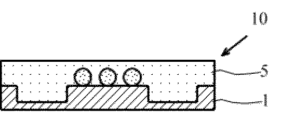
- the filler array film of the present invention can have another insulating resin layer laminated on at least one side of the insulating resin layer for holding the filler.
- another insulating resin layer 5 may be provided on the convex portion 4 side of the insulating resin layer for holding the filler
- another insulating resin layer 6 may be provided on the opposite side of the convex portion 4.
- the concave portion 3 may be penetrated to the insulating resin layer 6, and as shown in FIG. 9C, the convex portion 4 may be separated from the other convex portions by the penetrating concave portion 3 and made independent.
- the insulating resin layers 5 and 6 may be provided on both sides.
- the configuration of the other insulating resin layers 5 and 6 may be considered to be approximately the same as that described in the insulating resin layer for holding the filler 1.
- These separate insulating resin layers 5 and 6 can be formed from the same composition as the filler-retaining insulating resin layer 1.
- the composition may be changed or adjusted according to the purpose.
- the total resin layer thickness of the filler-arranged film including these layers is preferably 1 ⁇ m or more, more preferably 2 ⁇ m or more, even more preferably 3 ⁇ m or more, and preferably 30 ⁇ m or less, more preferably 15 ⁇ m or less, and even more preferably 8 ⁇ m or less.
- the other insulating resin layers 5 and 6 contain a black pigment, they can function as an insulating resin layer for forming a black matrix.
- the filler array film 10 of FIG. 8 when the filler array film 10 of FIG. 8 is sandwiched between the wiring board 100, which is the first article, and the ⁇ LED 200, which is the second article, and thermally compressed with a heat tool H, as shown in FIG. 12, a fillet F is formed on the side of the ⁇ LED 200 from the insulating resin layer 5, which is the insulating resin layer for forming a black matrix, and this fillet F can function as a black matrix.
- black pigments such as carbon black and titanium black can be used as the black pigment.
- titanium black is preferably used because it has an extremely low content of impurity ions and is itself insulating.
- the titanium black content in the black resin composition for black matrix is preferably 5% by mass or more, more preferably 10% by mass or more, preferably 40% by mass or less, more preferably 30% by mass or less.
- the average particle size of these black pigments is 10 to 100 nm. It is desirable that this black pigment is smaller than the average particle size of the filler.
- the filler array film of the present invention can be produced by a production method including the following steps A to C.
- This production method preferably includes step D following step C.
- Step A is a step of forming a filler-retaining insulating resin layer 1 on a release film (PET film) 30 that has been subjected to a release treatment, as shown in Fig. 13.
- the filler-retaining insulating resin layer can be formed by a conventional method, for example, by applying a filler-retaining insulating resin composition to a release film to form a film.
- step B a press mold 8 having a recess 7 corresponding to the protrusion of the filler-arranged film is brought into contact with the filler-retaining insulating resin layer 1 obtained in step A and heat-pressed to form a recess 3 and a protrusion 4 on one side of the filler-retaining insulating resin layer 1 (see FIG. 15).
- a release film may be interposed during the contact.
- the press mold 8 a single plate made of metal or resin having a recess 7 is preferable, but a roll having a recess 7 may also be used. A film having a recess 7 may also be used.
- As a method of heat pressing a general heat tool, a vacuum laminator, etc.
- the shape, depth, pitch, etc. of the recess 7 can be appropriately determined according to the shape, height, and pitch of the protrusion of the filler-arranged film (in other words, the shape, thickness, pitch, surface area, etc. of the second article to be connected).
- the depth of the recess 7 is preferably 1 ⁇ m or more, more preferably 2 ⁇ m or more, preferably 20 ⁇ m or less, and more preferably 10 ⁇ m or less.
- step C the filler arrangement surface of the filler transfer sheet 41, in which a plurality of fillers 2 are arranged on one side of the transfer substrate 40, is opposed to the top surface of the convex portion 4 of the filler-holding insulating resin layer 1, and pressed from the transfer substrate 40 side, thereby transferring a plurality of fillers 2 to the top surface of the convex portion 4.
- the filler transfer sheet 41 is peeled off and removed to obtain a filler array film 10 laminated on the release film 30, as shown in FIG. 17A.
- FIG. 18 shows an example of an optical microscope photograph of the filler array film 10 taken from the convex portion side.
- the filler 2 is arranged in a hexagonal lattice pattern on the surface of the convex portion 4, and no filler is present in the concave portion 3.
- the filler 2 is held on the surface of the adhesive transfer substrate 40 of the filler transfer sheet 41, but a transfer mold having a concave portion for accommodating the filler may be used as the transfer substrate 40.
- Step D In the method for producing the filler array film of the present invention, following step C, it is preferable to embed the filler 2 transferred to the top surface of the convex portion 4 in the filler-retaining insulating resin layer 1 by a known heat pressing method such as a heat press through another release film (PET film). This results in a filler array film 10 as shown in Figure 17B. A detailed description of the lamination of the other insulating resin layer will be omitted, but a laminated one may be prepared in advance, or may be laminated after step D.
- a known heat pressing method such as a heat press
- PET film release film
- one of the features of the manufacturing method of the filler-arranged film is the use of a press mold in step B.
- a press mold By using such a press mold, it is possible to obtain a filler-arranged film in which fillers are arranged only in the convex portions formed at the intended positions of the filler-arranged film, and which can essentially function as individual pieces.
- at least one or more filler groups can be arranged in the convex portions of the filler-arranged film, and the convex portions and concave portions can be arranged in the intended positions relative to the entire film.
- the film thickness of the concave portions is thin, they have excellent translucency and visibility.
- the presence of concave portions where no filler is present can greatly reduce the risk of short circuits when the filler-arranged film is used as an anisotropic conductive film.
- the filler-arranged film can be constructed from a single resin film, and other resin layers can also be laminated thereon, which has the advantage of increasing the degree of freedom in design.
- the filler transfer sheet 41 has filler 2 arranged on one side of the transfer substrate 40, but since the filler is not transferred to the recesses 3 of the filler-retaining insulating resin layer 1, the filler can be arranged randomly or regularly, preferably in a hexagonal lattice pattern, over the entire surface of the filler transfer sheet 41, making it easy to create the filler transfer sheet 41.
- the number density of the fillers in the filler transfer sheet 41 is the same as the number density of the fillers in the filler group of the filler array film.
- the filler array film of the present invention can be preferably applied to the filler array film of a connection structure in which a plurality of second articles are connected to a relatively large first article such as a wiring board via the filler array film, and can also be preferably applied to the filler array film in a method for manufacturing a connection structure characterized in that the filler array film is sandwiched between the first article and the second article, preferably so that the convex parts of the filler array film correspond to the second article, and then pressure-bonded (for example, by thermocompression).
- the second article and the convex parts of the filler array film may correspond to each other in a multiple-to-one or one-to-multiple manner, but from the viewpoint of ease of design and positional accuracy, it is preferable that they correspond to each other in a one-to-one manner.
- the first article and the second article have electrodes so that they can be electrically conductive when facing each other. It can also be used for conductive connection or anisotropic conductive connection by sandwiching the filler array film between the first article and the second article having opposing electrodes.
- connection structure of the present invention can be preferably applied to the manufacture of a connection structure in which the first article is a transparent display substrate with a transparent electrode arranged on one side, the second article is a ⁇ LED with an electrode formed on one side, the filler arranged on the convex portion of the filler-arranged film is a conductive particle, and the filler-arranged film itself functions as a conductive film or an anisotropic conductive film. Therefore, not only such a connection structure itself but also the manufacturing method thereof is another modified embodiment of the present invention. Note that an anisotropic conductive film can also be used instead of the conductive film.
- ⁇ LED display as a connection structure When manufacturing a ⁇ LED display using the filler array film of the present invention, in other words, when connecting the electrodes of the ⁇ LEDs and the electrodes of the substrate in a state where a plurality of ⁇ LEDs are regularly arranged on a wafer, first, the filler array film is aligned and attached to the electrodes of the substrate, and the filler array film and the ⁇ LEDs arranged on the wafer are aligned and attached to each other, and then heated and pressed to connect the electrodes of the ⁇ LEDs and the electrodes of the substrate.
- the connection may be made by heating and pressing in a two-stage manner (JP Patent Publication 2019-216097).
- connection may be made by reflow.
- connection structure has been described using a ⁇ LED display as an example, the connection structure of the present invention can also be applied to displays using larger light-emitting elements.
- the filler array film of the present invention is substantially in the form of individual pieces, but it can also be used as a filler array film in which the convex portions are completely separated from the entire film.
- the temporary attachment of the individualized filler array film can be performed using known methods such as a method using a stamp material or a laser (laser lift-off method) or a method that applies the same (for example, the methods described in JP-A-9-124020, JP-A-2011-76808, JP-A-6636017, JP-A-6187665, etc.), and is not particularly limited as long as the method can achieve the effects of the invention.
- known methods such as a method using a stamp material or a laser (laser lift-off method) or a method that applies the same can be used.
- Reference Example 1 ⁇ Formation of insulating resin layer for retaining conductive particles in anisotropic conductive film>
- the compositions (unit: parts by mass) having the formulation shown in Table 1 were uniformly mixed, and the resulting mixture was applied to a 50 ⁇ m-thick polyethylene terephthalate film that had been subjected to a release treatment to give a layer thickness as shown in Table 1.
- the mixture was then dried under conditions of 60° C. and 3 minutes to obtain an adhesive film as an insulating resin layer for retaining conductive particles.
- Reference Example 2 ⁇ Molds used in Examples and Comparative Examples> Assuming that ⁇ LEDs are mounted on a substrate using an anisotropic conductive film, the following stainless steel press dies 1 and 2 were prepared as press dies for forming convex portions in the insulating resin layer for retaining conductive particles of the anisotropic conductive film. Press 1 is used when one concave portion corresponds to one ⁇ LED, and press dies 2 is used when two concave portions correspond to one ⁇ LED.
- the anisotropic conductive films used in the examples and comparative examples were prepared according to Table 2. That is, in the case of the examples, stamping mold 1 or stamping mold 2 was placed on the insulating resin layer for holding conductive particles prepared in Reference Example 1, and stamping was performed using a vacuum laminator, thereby forming convex portions and concave portions in the insulating resin layer for holding conductive particles corresponding to the concave portions and non-convex portions of the stamping mold.
- the conductive particle arrangement surface of the conductive particle transfer sheet of Reference Example 3 was superimposed on the convex portion forming surface of the insulating resin layer for holding conductive particles, and the conductive particles were transferred only to the convex portions by heating and pressing with a heat tool, thereby obtaining an anisotropic conductive film.
- the conductive particle surface density in Example 1-7 is the surface density on the convex parts of the film, and the conductive particle surface density in Comparative Example 1-4 is the surface density over the entire surface of the film.
- connection structure for evaluating electrical resistance and insulation The Cr/Au layer of the glass substrate was patterned to match the convex pattern of the anisotropic conductive film of the Example, as shown in Fig. 21.
- the anisotropic conductive films of the Examples and Comparative Examples were aligned and attached to the obtained Cr/Au pattern of the glass substrate, a 1.5 cm square IC chip simulating a ⁇ LED was placed on it, and a connection structure for evaluating conductive resistance and insulation was obtained by thermocompression bonding under conditions of 150°C, 10 Pa, and 30 seconds.
- connection structure for evaluating visible light transmittance An IC chip having a size of 30 ⁇ m ⁇ 50 ⁇ m was prepared as a ⁇ LED for evaluating visible light transmittance. The IC chips were arranged in an area of 1.5 cm square and similarly thermocompression bonded to obtain a connection structure for evaluating visible light transmittance.
- connection structure for evaluating electrical resistance and insulation was measured for electrical resistance by a conventional method and evaluated according to the following criteria.
- the evaluation results are shown in Table 2. In practical use, an A or B rating is desirable.
- ⁇ Insulation evaluation> Regarding the insulation of the connection structure for evaluating the conductive resistance and insulation, 100 points between electrodes spaced 5 ⁇ m apart were selected, the resistance value of each was measured by a conventional method, the number of points where short circuits occurred was counted, and the insulation was evaluated according to the following criteria. The evaluation results are shown in Table 2. For practical purposes, an A, B, or C rating is desirable. A resistance of 10 7 ⁇ or less was judged as a short circuit.
- the average light transmittance of the connection structure for evaluating light transmittance to visible light of 400 to 700 nm was measured using a commercially available light transmittance measuring device and evaluated according to the following criteria. The evaluation results are shown in Table 2. For practical purposes, a rating of A, B, or C is desirable.
- the filler array film of the present invention allows for anisotropic conductive connection of fine-pitch ⁇ LEDs and other microelectronic components to a wiring board or the like, without the risk of short circuits, by making the convex portions of the filler array film essentially function as individual pieces of the filler array film, and furthermore, the filler array film of the present invention has a structure that can be formed using a simple transfer mold.
- the filler array film of the present invention has a structure comparable to that obtained by individualization using the laser lift-off method, and is useful for the manufacture of ⁇ LED displays.
- the filler array film of the present invention has been described using an anisotropic conductive film and an anisotropic conductive connection method using the same as an example, but the contents of that description can also be applied to a case where a conductive film and a conductive connection method using the same are used as an example, as long as the effects of the present invention are not impaired.
- REFERENCE SIGNS LIST 1 Filler-holding insulating resin layer 2, 2a Filler, conductive particles 3 Concave portion 4 Convex portion 5, 6 Another insulating resin layer 7 Concave portion of stamping die 8 Stamping die 10 Filler-arranged film 20, 20a, 20b Filler group 30 Release film 40 Transfer substrate 41 Filler transfer sheet 100 Wiring board 200 ⁇ LED F fillet H heat tool t 0 height of convex part t 1 depth of concave part w 1 width of concave part
Landscapes
- Chemical & Material Sciences (AREA)
- Engineering & Computer Science (AREA)
- Chemical Kinetics & Catalysis (AREA)
- Medicinal Chemistry (AREA)
- Polymers & Plastics (AREA)
- Organic Chemistry (AREA)
- Health & Medical Sciences (AREA)
- Microelectronics & Electronic Packaging (AREA)
- Manufacturing & Machinery (AREA)
- Non-Insulated Conductors (AREA)
- Compositions Of Macromolecular Compounds (AREA)
- Wire Bonding (AREA)
- Led Device Packages (AREA)
- Laminated Bodies (AREA)
Priority Applications (2)
| Application Number | Priority Date | Filing Date | Title |
|---|---|---|---|
| KR1020257031399A KR20250153822A (ko) | 2023-03-31 | 2024-03-21 | 필러 배열 필름 및 그 제조 방법 그리고 접속 구조체 및 그 제조 방법 |
| CN202480020872.6A CN120898330A (zh) | 2023-03-31 | 2024-03-21 | 填料排列膜及其制造方法以及连接结构体及其制造方法 |
Applications Claiming Priority (2)
| Application Number | Priority Date | Filing Date | Title |
|---|---|---|---|
| JP2023059074A JP2024146277A (ja) | 2023-03-31 | 2023-03-31 | フィラー配列フィルム及びその製造方法並びに接続構造体及びその製造方法 |
| JP2023-059074 | 2023-03-31 |
Publications (1)
| Publication Number | Publication Date |
|---|---|
| WO2024203689A1 true WO2024203689A1 (ja) | 2024-10-03 |
Family
ID=92904876
Family Applications (1)
| Application Number | Title | Priority Date | Filing Date |
|---|---|---|---|
| PCT/JP2024/010941 Ceased WO2024203689A1 (ja) | 2023-03-31 | 2024-03-21 | フィラー配列フィルム及びその製造方法並びに接続構造体及びその製造方法 |
Country Status (5)
| Country | Link |
|---|---|
| JP (1) | JP2024146277A (https=) |
| KR (1) | KR20250153822A (https=) |
| CN (1) | CN120898330A (https=) |
| TW (1) | TW202506857A (https=) |
| WO (1) | WO2024203689A1 (https=) |
Cited By (1)
| Publication number | Priority date | Publication date | Assignee | Title |
|---|---|---|---|---|
| WO2026074952A1 (ja) * | 2024-10-02 | 2026-04-09 | デクセリアルズ株式会社 | フィラー含有フィルム及びその製造方法並びに接続構造体及びその製造方法 |
Citations (5)
| Publication number | Priority date | Publication date | Assignee | Title |
|---|---|---|---|---|
| JP2003217354A (ja) * | 2002-10-04 | 2003-07-31 | Hitachi Chem Co Ltd | 接続部材 |
| JP2015056285A (ja) * | 2013-09-12 | 2015-03-23 | デクセリアルズ株式会社 | 接続構造体、及び異方性導電接着剤 |
| JP2020024932A (ja) * | 2012-08-24 | 2020-02-13 | デクセリアルズ株式会社 | 異方性導電フィルム及びその製造方法 |
| JP2020177916A (ja) * | 2014-12-22 | 2020-10-29 | デクセリアルズ株式会社 | 異方導電性フィルム及び接続構造体 |
| JP2022151818A (ja) * | 2021-03-26 | 2022-10-07 | デクセリアルズ株式会社 | 表示装置の製造方法 |
Family Cites Families (2)
| Publication number | Priority date | Publication date | Assignee | Title |
|---|---|---|---|---|
| TWI862897B (zh) | 2014-11-17 | 2024-11-21 | 日商迪睿合股份有限公司 | 異向性導電膜及連接構造體 |
| JP2022151822A (ja) | 2021-03-26 | 2022-10-07 | デクセリアルズ株式会社 | フィラー配列フィルム |
-
2023
- 2023-03-31 JP JP2023059074A patent/JP2024146277A/ja active Pending
-
2024
- 2024-03-19 TW TW113110095A patent/TW202506857A/zh unknown
- 2024-03-21 WO PCT/JP2024/010941 patent/WO2024203689A1/ja not_active Ceased
- 2024-03-21 CN CN202480020872.6A patent/CN120898330A/zh active Pending
- 2024-03-21 KR KR1020257031399A patent/KR20250153822A/ko active Pending
Patent Citations (5)
| Publication number | Priority date | Publication date | Assignee | Title |
|---|---|---|---|---|
| JP2003217354A (ja) * | 2002-10-04 | 2003-07-31 | Hitachi Chem Co Ltd | 接続部材 |
| JP2020024932A (ja) * | 2012-08-24 | 2020-02-13 | デクセリアルズ株式会社 | 異方性導電フィルム及びその製造方法 |
| JP2015056285A (ja) * | 2013-09-12 | 2015-03-23 | デクセリアルズ株式会社 | 接続構造体、及び異方性導電接着剤 |
| JP2020177916A (ja) * | 2014-12-22 | 2020-10-29 | デクセリアルズ株式会社 | 異方導電性フィルム及び接続構造体 |
| JP2022151818A (ja) * | 2021-03-26 | 2022-10-07 | デクセリアルズ株式会社 | 表示装置の製造方法 |
Cited By (1)
| Publication number | Priority date | Publication date | Assignee | Title |
|---|---|---|---|---|
| WO2026074952A1 (ja) * | 2024-10-02 | 2026-04-09 | デクセリアルズ株式会社 | フィラー含有フィルム及びその製造方法並びに接続構造体及びその製造方法 |
Also Published As
| Publication number | Publication date |
|---|---|
| TW202506857A (zh) | 2025-02-16 |
| KR20250153822A (ko) | 2025-10-27 |
| JP2024146277A (ja) | 2024-10-15 |
| CN120898330A (zh) | 2025-11-04 |
Similar Documents
| Publication | Publication Date | Title |
|---|---|---|
| US20250236712A1 (en) | Filler-containing film | |
| WO2016152791A1 (ja) | 異方導電性フィルム及び接続構造体 | |
| JP2017073389A (ja) | 異方性導電フィルム及び接続構造体 | |
| JP7087305B2 (ja) | フィラー含有フィルム | |
| JP7081097B2 (ja) | フィラー含有フィルム | |
| WO2024203689A1 (ja) | フィラー配列フィルム及びその製造方法並びに接続構造体及びその製造方法 | |
| WO2023054259A1 (ja) | フィラー含有フィルム | |
| KR102720762B1 (ko) | 필러 함유 필름 | |
| KR20240051204A (ko) | 도전 필름, 접속 구조체 및 그 제조 방법 | |
| TWI781213B (zh) | 異向性導電膜、連接結構體及彼等之製造方法 | |
| KR20250136396A (ko) | 필러 함유 필름, 접합체 및 그 제조 방법 | |
| JP2026064956A (ja) | フィラー含有フィルム及びその製造方法並びに接続構造体及びその製造方法 | |
| WO2026074952A1 (ja) | フィラー含有フィルム及びその製造方法並びに接続構造体及びその製造方法 | |
| WO2024195598A1 (ja) | フィラー含有フィルム | |
| JP2024136139A (ja) | フィラー含有フィルム、接続体及びその製造方法 | |
| JP2023050157A (ja) | フィラー含有フィルム | |
| HK40012110B (en) | Anisotropic electrically conductive film | |
| HK40012110A (en) | Anisotropic electrically conductive film | |
| HK40022374B (zh) | 各向异性导电膜 | |
| HK40022374A (en) | Anisotropic conductive film | |
| HK40008582A (en) | Filler-containing film | |
| HK40009152B (en) | Filler-containing film | |
| HK1240408A1 (en) | Anisotropic conductive film, manufacturing method for same, and connection structure |
Legal Events
| Date | Code | Title | Description |
|---|---|---|---|
| 121 | Ep: the epo has been informed by wipo that ep was designated in this application |
Ref document number: 24779812 Country of ref document: EP Kind code of ref document: A1 |
|
| ENP | Entry into the national phase |
Ref document number: 1020257031399 Country of ref document: KR Free format text: ST27 STATUS EVENT CODE: A-0-1-A10-A15-NAP-PA0105 (AS PROVIDED BY THE NATIONAL OFFICE) |
|
| WWE | Wipo information: entry into national phase |
Ref document number: 202480020872.6 Country of ref document: CN |
|
| WWP | Wipo information: published in national office |
Ref document number: 1020257031399 Country of ref document: KR |
|
| NENP | Non-entry into the national phase |
Ref country code: DE |
|
| WWP | Wipo information: published in national office |
Ref document number: 202480020872.6 Country of ref document: CN |
|
| 122 | Ep: pct application non-entry in european phase |
Ref document number: 24779812 Country of ref document: EP Kind code of ref document: A1 |